Embed Size (px)
Citation preview

1
High-Tc superconductivity in ultrathin Bi2Sr2CaCu2O8+x down to half-
unit-cell thickness by protection with graphene
Da Jiang1, Tao Hu1, Lixing You1, Qiao Li1, Ang Li1, Haomin Wang1, Gang Mu1, Zhiying Chen1,
Haoran Zhang1, Guanghui Yu1, Jie Zhu2, Qiujuan Sun1,3, Chengtian Lin4, Hong Xiao5,
Xiaoming Xie1,6, Mianheng Jiang1,6
1State Key Laboratory of Functional Materials for Informatics, Shanghai Institute of
Microsystem and Information Technology, Chinese Academy of Sciences, 865 Changning
Road, Shanghai 200050, China.
2Insititute of Precision Optical Engineering, School of Physics science and Engineering, Tongji
University, Shanghai 200092, China.
3School of Physics and Electronics, Central South University, Changsha 410083, China.
4Max-Planck-Institute für Festkörperforschung, 70569 Stuttgart, Germany.
5Beijing National Laboratory for Condensed Matter Physics, Institute of Physics, Chinese
Academy of Sciences, Beijing 100190, China.
6School of Physical Science and Technology, ShanghaiTech University, 319 Yueyang Road,
Shanghai 200031, China.
Correspondence and requests for materials should be addressed to D.J.
([email protected]) or T.H. ([email protected]).

2
Abstract
High-Tc superconductors confined to two dimension exhibit novel physical phenomena,
such as superconductor-insulator transition. In the Bi2Sr2CaCu2O8+x (Bi2212) model system,
despite extensive studies, the intrinsic superconducting properties at the thinness limit have
been difficult to determine. Here we report a method to fabricate high quality single-crystal
Bi2212 films down to half-unit-cell thickness in the form of graphene/Bi2212 van der Waals
heterostructure, in which sharp superconducting transitions are observed. The heterostructure
also exhibits a nonlinear current-voltage characteristic due to the Dirac nature of the graphene
band structure. More interestingly, although the critical temperature remains essentially the
same with reduced thickness of Bi2212, the slope of the normal state T-linear resistivity varies
by a factor of 4-5, and the sheet resistance increases by three orders of magnitude, indicating a
surprising decoupling of the normal state resistance and superconductivity. The developed
technique is versatile, applicable to investigate other two-dimensional (2D) superconducting
materials.
Introduction
Two-dimensional superconductors provide insights into the mechanisms of
superconductivity and their possible device applications1-11. Bi2212 is a quasi-2D cuprate in
which thin superconducting sheets (CuO2) alternate with insulating layers (SrO, BiO). Its
extreme anisotropy12-15 makes Bi2212 an ideal material to address the fundamental question
whether superconductivity truly survives down to half-unit-cell thickness which may in turn

3
help to answer another fundamental question: what the superconducting mechanisms are in the
ultrathin Bi2212. The superconducting properties of ultrathin Bi2212 have already been studied
in both bottom-up4,5 (thin-film growth) and top-down6 (micro-fabrication of single crystal)
approaches. Unfortunately, these approaches have yielded inconsistent results, with behavior
ranging from insulating to superconducting. Molecular beam epitaxy (MBE) method has been
used to grow half-unit-cell-thick Bi2212 (HUC-Bi2212) sandwiched in between multiple
Bi2201 blocks8,9. In these ultrathin MBE superlattices, the resulting superconducting properties
depend on the sandwich structure16-19, which results in uncertainty about the properties originate
from HUC-Bi2212 or from the superlattice stack. Inspired by the successful isolation of
graphene by micromechanical exfoliation20, researchers have prepared many 2D materials of
extremely high quality using this unique and versatile technique, including MoS2, NbSe2, and
single-unit-cell-thick Bi2212 (SUC-Bi2212), which was shown to be insulating7. Recently, the
use of a van der Waals heterostructure composed of graphene and other 2D atomic crystals has
emerged as a promising approach to pursue condensed matter physics questions in these
systems21, such as Hofstadter’s butterfly effect and the fractal quantum Hall effect. This
structure, which is artificially constructed by stacking different 2D crystals on top of each other,
exhibits many unusual properties21,22, such as quantum capacitance and moiré patterns.
Here we use mechanical exfoliation method to study the intrinsic properties of Bi2212,
from half-unit-cell thickness to bulk material, by producing thin films of graphene/Bi2212 van
der Waals heterostructures. In addition to superconducting transition above the liquid nitrogen
temperature observed in all the samples, we were surprised to find the decoupling of the normal
state resistance and superconductivity, which contrasts with previous reports23 on their

4
importance to the superconducting mechanism.
Results
Temperature dependence of resistance in graphene/SUC-Bi2212
Samples were prepared by mechanical exfoliation method (Fig. 1). Four-probe
measurements were performed on graphene/Bi2212 heterostructure samples at the temperature
(T) from 2 to 300 K by using direct current (dc) combined with alternating current (ac) (Idc+Iac).
Superconductivity was observed in all samples even at half-unit-cell thickness, although the
success rate for the preparation of the HUC2212 heterostructure was lower.
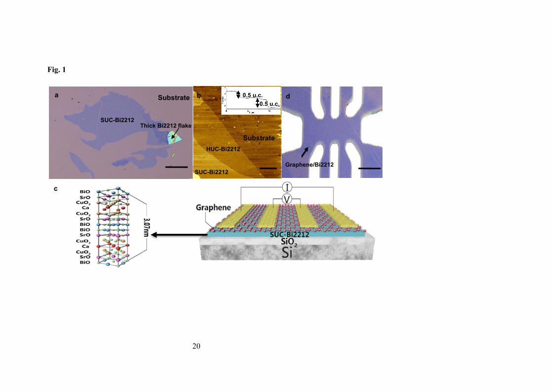
We observed a sharp resistive transition above the liquid nitrogen temperature (at 88 K)
regardless of Idc bias in the 0 to 0.36 mA range examined (Fig. 2a), indicating that robust
superconductivity is preserved. In the heterostructure, graphene and SUC-Bi2212 form a
parallel circuit as illustrated in the inset to Fig. 2a. We also observed residual resistance in the
superconducting state, as a result of partial current flowing through the graphene protection
layer (although we eliminated this by converting the graphene to an insulator, as discussed in
the next subsection). For small bias currents (less than 0.12 mA in our case) in the
superconducting temperature range, the differential resistance increased with decreasing
temperature, which suggests opening of a superconducting gap. In contrast, the differential
resistance in the superconducting state became independent of temperature at high bias current,
which overcomes the gap. After subtracting the temperature independent resistance component

5
from the data, all the curves precisely overlap with one another (Fig. 2b), indicating the
consistency and reliability of our measurements and the reproducibility of our fabrication
technique. Furthermore, different samples with the same thickness can be scaled with each other
(Fig. 2c). The R-T curves in Fig. 2b thus reflect the intrinsic superconducting properties of SUC-
Bi2212.
We also observed a T independent parabolic-like fixed offset I-V curve in the
superconducting state of the graphene/SUC-Bi2212 heterostructure (Fig. 2d). This non-
vanished voltage originates from the two junctions between SUC-Bi2212 and graphene as
illustrated in the inset of Fig. 2a. Graphene is known to be a Dirac fermion material with linear
energy dispersion at the Dirac point20. The differential conductance of the junction dI/dV is a
result of tunneling from graphene to SUC-Bi2212. The value is thus proportional to the product
of the density of states of graphene (ngraphene) and SUC-Bi2212 (nSUC-Bi2212), which is dI/dV∝
nSUC-Bi2212×ngraphene (Ref. 26). The value of nSUC-Bi2212 is not affected by the voltage in the
superconducting state because there is zero electric field inside the superconductor, however,
ngraphene is proportional to the bias voltage (Vg) across the junction (Vg∝ngraphene) (Ref. 27).
When performing I-V measurements below Tc, the voltage (V) drops only at the graphene/SUC-
Bi2212 junctions, which is V=2Vg. Therefore, we obtain dI/dV∝V, hence, I∝V2, which is
precisely the parabolic offset of the I-V curves presented in Fig. 2d. The voltage actually drives
the single layer graphene away from the Dirac point and tunes its density of states, which yields
a parabolic I-V curve.
The role of graphene in the heterostructure
6
SUC-Bi2212 is known to be insulating6,7. The present investigation confirms that ultrathin
Bi2212 transforms into an insulator if graphene is not transferred onto it. This observation
suggests that one of the major roles of graphene is to protect the underlying ultrathin Bi2212,
because graphene is highly impermeable even to small atoms such as helium28.
To verify that the residual resistance is a result of the current bypass effect, we converted
the graphene capping layer into an insulator by oxidation29. Interestingly, this caused the SUC-
Bi2212 heterostructure to become non-superconducting. We achieved zero resistance in a two-
unit-cell-thick Bi2212 (TUC-Bi2212)-based heterostructure as expected (Fig. 3a&b). However,
after oxidation, the temperature range associated with the transition was more than twice that
observed before oxidation, and Tc was decreased slightly (Fig. 3d). Graphene/SUC-Bi2212 and
graphene/TUC-Bi2212 heterostructures fabricated together were measured before oxidation,
and both were superconducting. After oxidation, TUC-Bi2212 remained superconductive and
reached zero resistance (Fig. 3a), whereas SUC-Bi2212 lost its superconductivity. This was not
a result of destruction of graphene. If the graphene/SUC-Bi2212 sample had been damaged and
had lost its superconductivity, the resistance would have gone up to several hundred mega-
ohms based on our investigations. In our case, the resistance of SUC-Bi2212 was only several
kilo-ohms after oxidation. This suggested that SUC-Bi2212 was not destroyed completely by
oxidation.
Investigation on the normal state with reduced thickness
The preservation of superconductivity in ultrathin films provides a rare opportunity to
explore insights on the nature of superconductivity. In particular, it allows us to test whether

7
correlations between certain transport properties and superconductivity are important to the
pairing mechanism, as previously suggested23.
It is well known that the resistivity of cuprates around optimal doping increases linearly
with increasing temperature over a wide range (often described as T-linear ρ)30. We found that
the resistance of Bi2212 in the normal state increased linearly with increasing temperature not
only at 270-unit-cell thickness (which can be considered a bulk material, because its R-T curve
is the same as that of the bulk31), but even down to half-unit-cell thickness (Fig. 4a). In addition,
the slope decreases symmetrically with reduced thickness (Fig. 4b).
The slope of this linear resistivity (A), which represents the strength of the scattering,
scales with Tc in bulk cuprate, organic, and pnictide superconductors23 (as demonstrated by the
pink squares, olive circles, and blue triangles in Fig. 4c, respectively). However, the empirical
correlation between A and Tc fails in the graphene/ultrathin Bi2212 heterostructure (black stars
in Fig. 4c), in which A changes by a factor of 4-5, whereas Tc varies by only about 10%. We
note that the range of A values in our data is much larger than that presented in previous data,
in which A remained very small, demonstrating the robustness of our conclusions.
Although the sheet resistance (R□) in the normal state of Bi2212 increased from ohms to
kilo-ohms as the thickness was reduced from 270 unit cells to 0.5 unit cells, Tc remained almost
the same (Fig.4a&d). In contrast, the result from ultrathin amorphous Mo-Ge films (blue
diamonds in Fig. 4d) showed that Tc decreases rapidly with increasing sheet resistance32, which
is attributed to disorder induced Anderson localization and increased Coulomb interaction33.
This discrepancy suggests that the increase in R□ with reduced thickness in Bi2212 is unrelated

8
to disorder. Instead, this increase may be related to a decrease in the number of conducting
paths through inter-plane coupling between CuO2 layers, a process unrelated to Tc.
Discussion
Robust superconductivity has already been reported in some atomically thin conventional
superconductors34-36. Our investigations reveal that this phenomenon could also be observed in
high-Tc superconductor. Superconductivity can be preserved in ultrathin Bi2212 even at half-
unit-cell thickness, with the protection of graphene. The I-V behavior from the combined
graphene/SUC-Bi2212 structure may inspire the development of new superconducting devices
that benefit from both the robust electronic properties of graphene and the high speed of
superconductivity.
In addition to graphene being crucial for the preservation of superconductivity in ultrathin
Bi2212, the normal state behaviors of Bi2212 with reduced thickness are also essential to
understanding high-Tc superconductivity. Normal state transport in cuprates is considered to be
strongly related to the pairing mechanism23. Surprisingly, in a sample of graphene/ultrathin
Bi2212 heterostructure the normal state properties were decoupled from the superconductivity.
The disconnection of A and Tc brings into question the link between the large angle scattering
process and the superconductivity mechanism, which suggests the need to search for other
avenues to further understand the origin of high-Tc superconductivity in cuprates. Therefore,
graphene/ultrathin Bi2212 heterostructure samples provide a promising platform to obtain

9
further insight into the underlying mechanisms of superconductivity and for the exploration of
new devices.
Methods
Exfoliation of Bi2212
A 5 mm-wide and 0.5 mm-thick platelet of single-crystal Bi2212 was exfoliated using
scotch tape and transferred onto a SiO2/Si substrate (SiO2-300 nm; Si-500 μm)37. Bi2212 always
cleaves between two BiO planes, in which Van der Waals-type bonding is present38. To select
ultrathin Bi2212 flakes from the exfoliated flakes on the substrate, a combination of optical
microscope and atomic force microscope was used27.
Transfer of chemical vapour deposition (CVD) graphene
Continuous graphene films with domains larger than 100×100 μm2 were grown on 1×1
cm2, 25 μm thick polished copper foil (Alfa Aesar) using CVD39. The as-grown graphene on
Cu was spin-coated with poly-methyl methacrylate (PMMA) and then covered with a piece of
tape. Ammonium persulphate (0.1 M) was used to dissolve the copper foil39. The tape-PMMA-
graphene was then dry transferred on top of the substrate with Bi2212 flakes immediately after
the flakes were cleaved. To obtain a clean surface and better contacts between graphene and
Bi2212, thermal annealing was performed in O2/Ar (20 sccm/200 sccm) at 200°C for 30
minutes in a tube furnace40 after removing the PMMA and the tape with acetone. Contamination
at the interface of the heterostructure can clean itself41-43.

10
Device fabrication
The microfabrication process that has been applied for graphene-based devices27, was used
to prepare devices from a graphene/Bi2212 van der Waals heterostructure. A mask aligner was
used to create an electrode pattern on top of the heterostructures. Then, a layer of 50 nm Au/5
nm Cr was deposited by electron-beam deposition followed by standard lift-off procedures.
After device fabrication and initial transport measurements, the heterostructure was
exposed to ultraviolet light in ozone29 to oxidize the graphene protection layer and achieve zero
resistance in the superconducting state.
References
1. Shalnikov, A.I. Superconducting thin films. Nature 142, 74 (1938).
2. Hetel, I., Lemberger, T. R. & Randeria, M. Quantum critical behavior in the superfluid
density of strongly underdoped ultrathin copper oxide films. Nature Physics 3, 700-702
(2007).
3. Bollinger, A. T. et al. Superconductor–insulator transition in La2-xSrxCuO4 at the pair
quantum resistance. Nature 472, 458-460 (2011).
4. Sugimoto, T., Yoshida, M., Sugawara, K., Shiohara, Y. & Tanaka, S. Preparation of
ultrathin Bi-Sr-Ca-Cu-O superconducting films by metal organic chemical vapor
deposition. Appl. Phys. Lett. 58, 1103-1105 (1991).

11
5. Saito, K. & Kaise, M. Superconductivity and structure of a few-unit-cells-thick Bi-Sr-Ca-
Cu-O ultrathin films. Phys. Rev. B, 57, 11786-11791 (1998).
6. You, L. X., Yurgens, A., Winkler, D., Lin, C. T. & Liang, B. Thickness dependence of the
superconducting properties of ultra-thin Bi2Sr2CaCu2O8+x single crystals. Supercond. Sci.
Technol. 19, S205-S208 (2006).
7. Novoselov, K. S.et al. Two-dimensional atomic crystals. Proc. Natl. Acad. Sci.102, 10451-
10453 (2005).
8. Bozovic, I. et al. Superconductivity in epitaxial Bi2Sr2CuO6/Bi2Sr2CaCu2O8 superlattices:
the superconducting behavior of ultrathin cuprate slabs. J. Supercond. 5, 19 (1992).
9. Li, Z. Z. et al. Synthesis of Bi2Sr2CaCu2O8/Bi2Sr2CuO6 superlattices with Tc enhancement
effect. Phys. Rev. Lett. 72, 4033 (1994).
10. Kosterlitz, J. M. & Thouless, D. J. Ordering, metastability and phase transitions in two-
dimensional systems. J. Phys. C 6, 1181-1203 (1973).
11. Guo, Y. et al. Superconductivity modulated by quantum size effects. Science 306, 1915-
1917 (2004).
12. Watanabe, T., Fujii, T. & Matsuda, A. Anisotropic resistivities of precisely oxygen
controlled single-crystal Bi2Sr2CaCu2O8+δ: systematic study on “spin gap” effect. Phys.
Rev. Lett. 79, 2113-2116 (1997).
12
13. Martin, S., Fiory, A. T., Fleming, R. M., Schneemeyer, L. F. & Waszczak, J. V.
Temperature dependence of the resistivity tensor in superconducting Bi2Sr2.2Ca0.8Cu2O8
crystals. Phys. Rev. Lett. 60, 2194-2197 (1988).
14. Kleiner, R. et al. Intrinsic Josephson effects in Bi2Sr2CaCu2O8 single crystals. Phys. Rev.
Lett. 68, 2394 (1992).
15. Kleiner, R. & Muller, P. Intrinsic Josephson effects in high-Tc superconductors. Phys. Rev.
B 49, 1327 (1994).
16. Gozar, A. et al. High-temperature interface superconductivity between metallic and
insulating copper oxides. Nature 455, 782 (2008).
17. Mannhart, J. & Schlom, D. G. Oxide interfaces -- an opportunity for electronics. Science
327, 1607 (2010).
18. Bozovic, I., et al. Epitaxial strain and superconductivity in La2−xSrxCuO4 thin films. Phys.
Rev. Lett. 89, 107001 (2002).
19. Butko, V. Y., et al. Madelung strain in cuprate superconductors -- a route to enhancement
of the critical temperature. Adv. Mater. 21, 3644 (2009).
20. Novoselov, K. S. et al. Two-dimensional gas of massless Dirac fermions in graphene.
Nature 438, 197-200 (2005).
21. Geim, A. K. & Grigorieva, I. V. Van der Waals heterostructures. Nature 499, 419-425
(2013).

13
22. Ponomarenko, L. A. et al. Tunable metal–insulator transition in double-layer graphene
heterostructures. Nature Phys. 7, 958–961 (2011).
23. Taillefer, L. Scattering and pairing in cuprate superconductors. Annual Review of
Condensed Matter Physics 1, 51-70 (2010).
24. Guggisberg, M. et al, Separation of interactions by noncontact force microscopy. Phys. Rev.
B 61, 11151 (2000).
25. Pan, S. H., Hudson, E. W., Ma, J. & Davis, J. C. Imaging and identification of atomic
planes of cleaved Bi2Sr2CaCu2O8+δ by high resolution scanning tunneling microscopy.
Appl. Phys. Lett. 73, 58-60 (1998).
26. Duke, C. B. Tunneling in Solids (Academic Press, New York and London, 1969).
27. Novoselov, K. S.et al. Electric field effect in atomically thin carbon films. Science 306,
666-669 (2004).
28. Bunch, J. S.et al. Impermeable atomic membranes from graphene sheets. Nano Lett. 8,
2458-2462 (2008).
29. Leconte, N., et al. Damaging graphene with ozone treatment: a chemically tunable metal-
insulator transition. ACS Nano 4 (7), 4033 (2010).
30. Ito, T., Takenaka, K. & Uchida, S. Systematic deviation from T-linear behavior in the in-
plane resistivity of YBa2Cu3O7-y: Evidence for dominant spin scattering. Phys. Rev. Lett.
70, 3995–3998 (1993).

14
31. Oh, S., Luccio, T. D. & Eckstein, J. N. T linearity of in-plane resistivity in Bi2Sr2CaCu2O8+δ
thin films. Phys. Rev. B 71, 052504 (2005).
32. Graybeal, J. M. & Beasley, M. R. Localization and interaction effects in ultrathin
amorphous superconducting films. Phys. Rev. B 29, 4167 (1984).
33. Anderson, P. W., Muttalib, K. A. & Ramakrishnan, T. V. Theory of the "universal"
degradation of Tc in high-temperature superconductors. Phys. Rev. B 28, 117 (1983).
34. Qin, S., Kim, J., Niu, Q. & Shih, C. Superconductivity at the two-dimensional limit. Science
324, 1314-1317 (2009).
35. Zhang, T. et al. Superconductivity in one-atomic-layer metal films grown on Si(111).
Nature Physics 6, 104-108 (2010).
36. Yamazaki, S. et al. Metallic transport in a monatomic layer of In on a silicon surface. Phys.
Rev. Lett. 106, 116802 (2011).
37. Geim, A. K. & Kim, P. Carbon wonderland. Scientific American, 90-97(April 2008).
38. Pan, S. H., Hudson, E. W., Ma, J.& Davis, J. C. Imaging and identification of atomic planes
of cleaved Bi2Sr2CaCu2O8+δ by high resolution scanning tunneling microscopy. Appl. Phys.
Lett. 73, 58-60 (1998).
39. Li, X. et al. Large-area synthesis of high-quality and uniform graphene films on copper
foils. Science 324, 1312-1314 (2009).

15
40. Britnell, L. et al. Field-effect tunneling transistor based on vertical graphene
heterostructures. Science 335, 1140-1143(2012).
41. Haigh, S. J. et al. Cross-sectional imaging of individual layers and buried interfaces of
graphene-based heterostructures and superlattices. Nat. Mater.11, 764-767 (2012).
42. Georgiou, T. et al. Vertical field-effect transistor based on graphene WS2 heterostructures
for flexible and transparent electronics. Nat. Nanotechnol. 8, 100-103 (2013).
43. Lui, C. H., Liu, L., Mak, K. F., Flynn, G. W. & Heinz, T. F. Ultraflat graphene. Nature 462,
339-341 (2009).
Acknowledgments
We sincerely thank Z. X. Shen, D.H. Lee, A.K. Geim, S.Q. Shen for discussions during
the preparation of this manuscript.
This work was partially supported by the Strategic Priority Research Program (B) of the
Chinese Academy of Sciences (Grant No. XDB04010400, XDB04040300 and XDB04020000),
National Science and Technology Major Project (Grant No. 2011ZX02707), the National
Natural Science Foundation of China (Grant No. 11104303, 11274333, 11204339, 11104335,
and 61136005), Chinese Academy of Sciences (Grant No.KGZD-EW-303KJCX2-EW-W11,
and XDA02040000), Hundred Talents Program of CAS, CAS International Collaboration and
Innovation Program on High Mobility Materials Engineering, Science and Technology

16
Commission of Shanghai Municipality (Grant No. 12JC1410100 and 12JC1403900), and the
Ministry of Science and Technology of China (Grant No. 2011CBA00107 and 2012CB921302).
Author contributions
D.J. planned the research and produced the samples. D.J. and T.H. designed the
experiments. T.H. And Q.L. performed the measurements. T.H. analyzed the data. Z.C., H.Z.,
and G.Y. grew graphene by CVD. C.L. grew the Bi2212 single crystals. D.J., Q.S., and J.Z.
performed the micro-fabrication. D.J., T.H., L.Y., A.L., H.W., G.M., H.X., X.X., and M.J.
discussed the results. D.J. and T.H. wrote the paper. M.J. and X.X. supervised the work.
Additional Information
Competing financial interests: The authors declare no competing financial interests.
Figure Legends
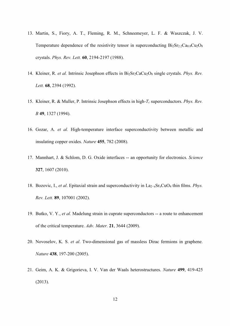
Fig. 1. Graphene/Bi2212 heterostructure. (a) Optical-microscope image (in white light) of
several Bi2212 flakes included HUC-Bi2212 and SUC-Bi2212 (see the Methods section for the
detailed fabrication procedure). Colors: light purple--SiO2/Si substrate; blue--SUC-Bi2212
flake; light blue--the thick Bi2212 flake. Scale bar: 20 μm. (b) Atomic force microscope image
of a Bi2212 flake. Color: dark yellow--HUC-Bi2212; bright yellow--SUC-Bi2212; brown--

17
SiO2/Si substrate. The inset shows the AFM profile of the flake. The lower step is
approximately 2.7 nm and the upper step is approximately 2.3 nm. However, one should
consider that the thickness measured by AFM includes the chemical and van der Waals
contrasts24 and the distance between Bi2212 and SiO2, so that the measured thickness is always
larger than the theoretical values and the differences vary from sample to sample with a typical
value of around 1 nm. The theoretical thicknesses of HUC-Bi2212 and SUC-Bi2212 are 1.5 nm
and 3 nm, respectively, so that for thicknesses of 2.7 nm and 2.3 nm, they can only be half-unit-
cell-thick. Scale bar: 5 μm. (c) Schematic view of the device. The SUC-Bi2212 flakes were
prepared by micromechanical exfoliation of a bulk Bi2212 single crystal, which cleaves
between two BiO planes, and for which van der Waals-type25 bonding is present. Each unit cell
consists of two CuO2-bilayer blocks sandwiched in between Sr-Bi-O charge reservoir layer.
Single-layer graphene prepared by using chemical vapour deposition (CVD) was then
transferred on top of the SUC-Bi2212 flakes. The electrodes were prepared using
microfabrication techniques. (d) An optical image of one of our experimental devices prepared
from a graphene/Bi2212 van der Waals heterostructure sample. Scale bar: 10 μm. u.c. = unit
cell.
Fig. 2. Typical changes in temperature dependence with differential resistance. (a) R-T
curves for graphene/SUC-Bi2212 van der Waals heterostructures measured at applied bias
currents of Idc= 0, 0.04, 0.08, 0.16, 0.20, 0.24, 0.28, 0.32, and 0.36 mA. The transition
temperature (Tc) of each thickness was defined as the intersection of the two straight lines. Inset:

18
brief circuit diagram of the transport measurement. (b) R-T curves for graphene/SUC-Bi2212
heterostructures with different bias currents. Idc = 0.16, 0.20, 0.24, 0.28, 0.32 and 0.36 mA, after
subtraction of the differential resistance for the interface between graphene and SUC-Bi2212.
(c) Temperature dependence of normalized resistance curves for three graphene/SUC-Bi2212
heterostructure samples after subtraction of the temperature independent residual sheet
resistance (typically several ohms): Sample 1 (black line), Sample 2 (olive line), and Sample 3
(blue line). These three curves are normalized at 250 K and can be scaled with each other. (d)
I-V curves for graphene/SUC-Bi2212 van der Waals heterostructure measured at 10 K ≤ T ≤
300 K.
Fig. 3. Comparison between graphene and graphene-oxide protection layers. (a) R-T
curves for a graphene/TUC-Bi2212 van der Waals heterostructure sample before and after
oxidation of the graphene protection layer. The orange curve represents the sample with the
graphene protection layer, black curve represents the same sample after oxidation of the
graphene protection layer. (b) Normalized (250 K) R-T curves of (a). (c) Illustration of the
device before and after oxidation. The active area decreases after oxidation as a result of etching
by oxygen, which partially contributes to the change in the resistance in the normal state. (d)
Expanded version of the data in (b). The transition width is defined as the range between Tc and
the temperature with 10% resistance of Tc’s.
Fig. 4. R-T behavior of ultrathin Bi2212. (a) R-T curves for Bi2212 with various thicknesses

19
from 270-unit-cell-thick to half-unit-cell-thick. (b) Temperature dependence of normalized
(250 K) sheet resistance of Bi2212 with thickness ranging from 270 unit cells to a half unit cell.
The solid lines represent samples in this investigation. The dark cyan diamond dots represent
the bulk Bi2212 in Reference 31. (c) A versus Tc/Tcmax. A is the slope for T-linear ρ in the normal
state. Tcmax is Tc of the optimally doped bulk sample. Tc
max is 93 K for Bi2212, 90 K for
Tl2Ba2CuO6+δ, 1.1 K for (TMTSF)2PF6, and 26 K for Ba(Fe1-xCox)2As2. The black stars
represent graphene/ultrathin Bi2212, the pink squares represent Tl2Ba2CuO6+δ, the olive circles
represent (TMTSF)2PF6, and the blue triangles represent Ba(Fe1-xCox)2As2 in Ref. 23. (d) Sheet
resistance in the normal state wersus Tc. The black stars are taken from Fig. 4a and the blue
diamonds represent Mo79Ge21, acquired from Ref. 32. Tcmax is 7.2 K for Mo79Ge21. u.c. = unit
cell.
20
Fig. 1
a
SUC-Bi2212
Substrate
Thick Bi2212 flake
b
Substrate
SUC-Bi2212
HUC-Bi2212
0.5 u.c.
0.5 u.c.
Graphene/Bi2212
d
c
21
Fig. 2
a
b
c
Graphene/SUC-Bi2212
d

22
Fig. 3
a
b
TUC-Bi2212
d
c Before Oxidation
After Oxidation

23
Fig. 4
a b
c
d
(Ref. 23)
(Ref. 32)
(Ref. 23)
(Ref. 23)
31