Embed Size (px)
Citation preview
HIGH THERMAL CONDUCTIVITY PCB SOLUTIONS MANUFACTURING
SINCE 2010
1
RUSALOX is a high-technology developer and producer of substrates and LED modules with high thermal conductivity • The innovative RUSALOX products based on ALOXIDE technology are in a high demand on Russian LED market • Efficiency and economic feasibility confirmed by multiple tests results and mass production with over hundreds of installations in Russia. • RUSALOX collaborates with developers for creating and testing prototypes of the most effective products with outstanding competitive advantages. • RUSALOX is focused on Russian commercial, industrial and outdoor segments of LED market exceeding $250 million in 2013 • In 2015 RUSALOX started expansion on international markets Key advantages: • Unique aluminum oxide technology – the best solution for efficient thermal management in powerful LED lighting • Strong partnerships with market leaders • Strong technical and engineering team Production facilities are located in Vladimir, 180 km from Moscow: • Production space: 2 500 m2 • Capacity: 1,5 mln dm2
ABOUT
2
THERMAL MANAGEMENT CHALLENGE AND WELL-KNOWN FACTS
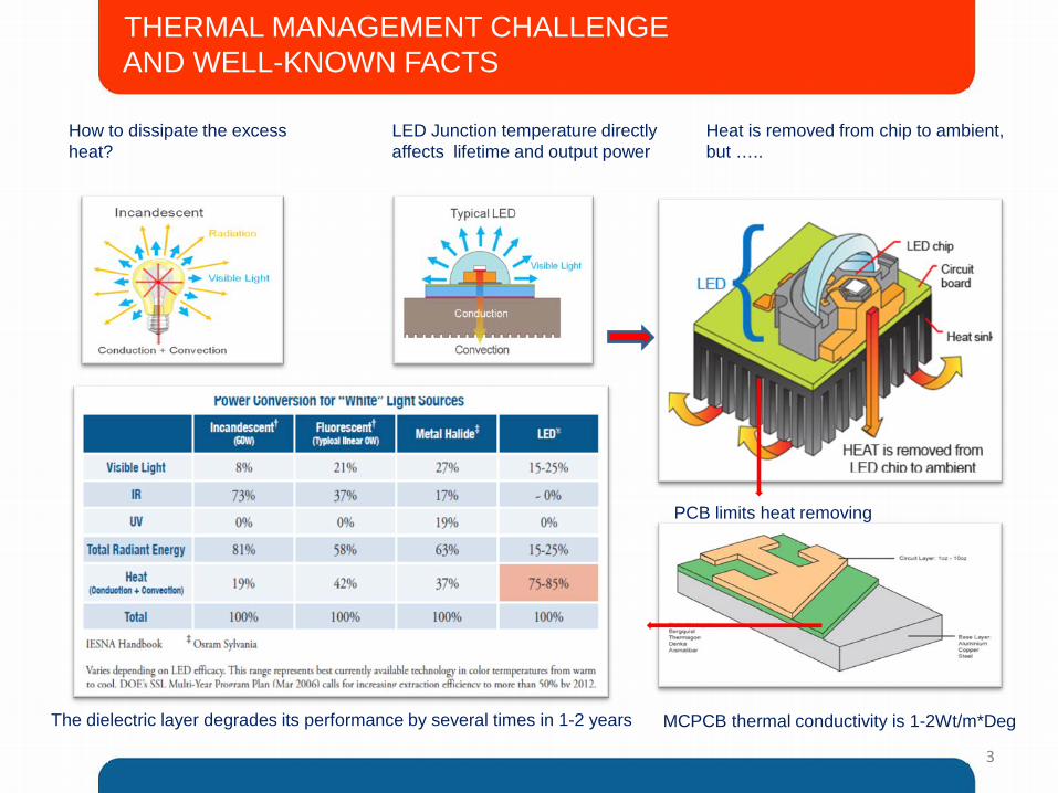
How to dissipate the excess heat?
Heat is removed from chip to ambient, but …..
PCB limits heat removing
MCPCB thermal conductivity is 1-2Wt/m*Deg The dielectric layer degrades its performance by several times in 1-2 years
LED Junction temperature directly affects lifetime and output power
3
MARKET REQUEST
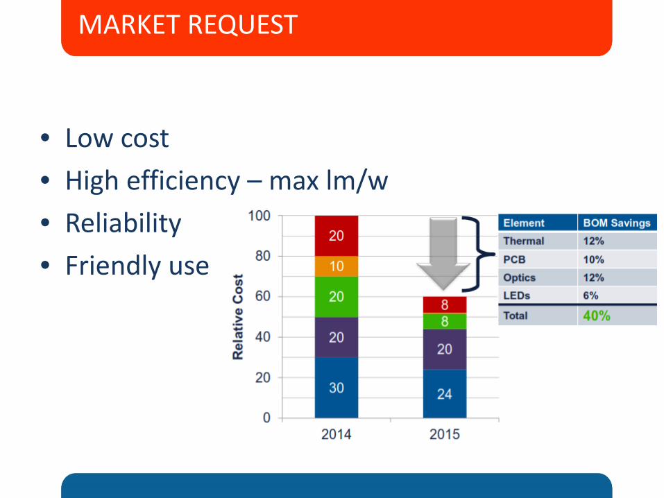
• Low cost • High efficiency – max lm/w • Reliability • Friendly use
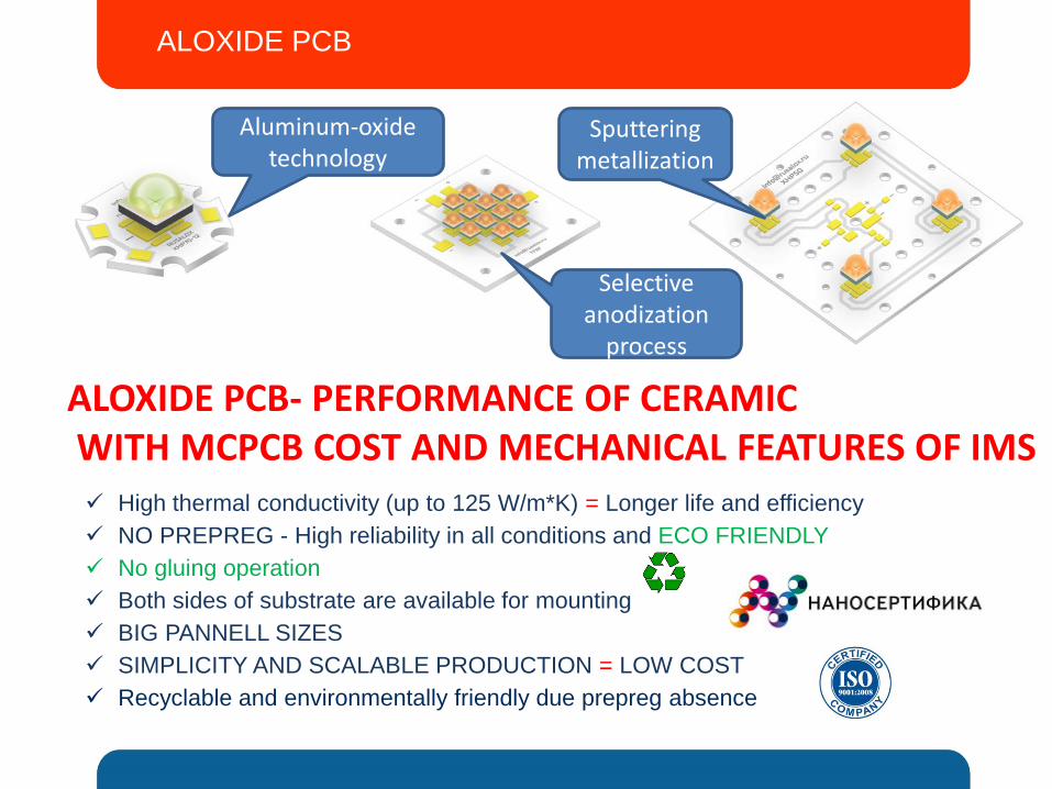
ALOXIDE PCB
MCPCB CERAMIC PCB
High thermal conductivity (up to 125 W/m*K) = Longer life and efficiency NO PREPREG - High reliability in all conditions and ECO FRIENDLY No gluing operation Both sides of substrate are available for mounting BIG PANNELL SIZES SIMPLICITY AND SCALABLE PRODUCTION = LOW COST Recyclable and environmentally friendly due prepreg absence
Aluminum-oxide technology
Selective anodization
process
Sputtering metallization
ALOXIDE PCB- PERFORMANCE OF CERAMIC WITH MCPCB COST AND MECHANICAL FEATURES OF IMS
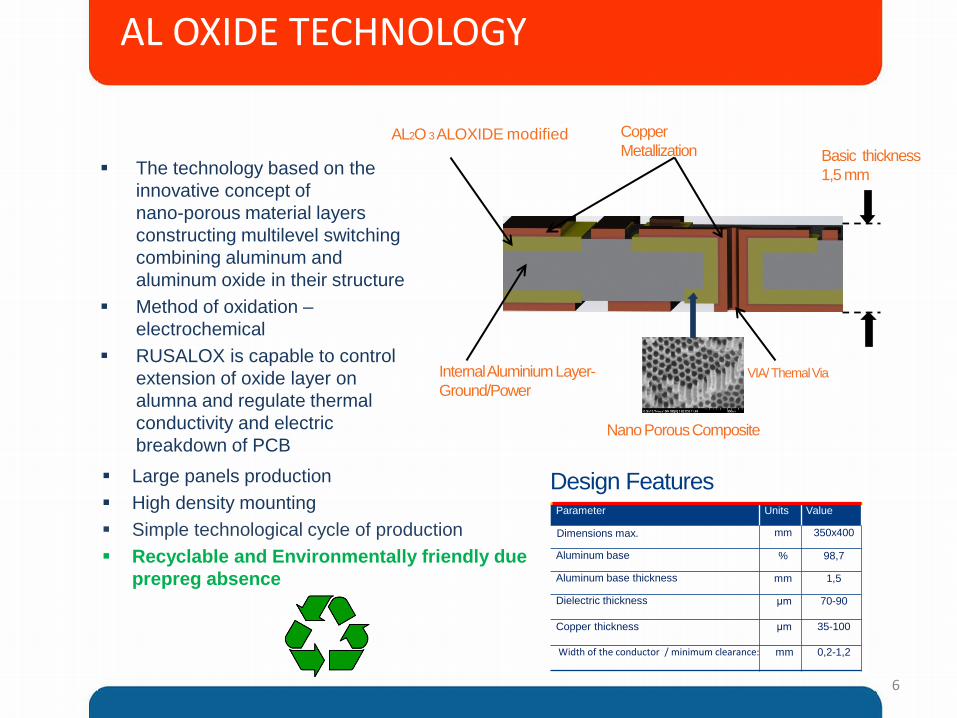
AL OXIDE TECHNOLOGY
The technology based on the innovative concept of nano-porous material layers constructing multilevel switching combining aluminum and aluminum oxide in their structure
Method of oxidation –electrochemical
RUSALOX is capable to control extension of oxide layer on alumna and regulate thermal conductivity and electric breakdown of PCB Large panels production
High density mounting Simple technological cycle of production Recyclable and Environmentally friendly due
prepreg absence
VIA/ Themal Via
Copper Metallization
6
AL2O 3 ALOXIDE modified
Nano Porous Composite
Internal Aluminium Layer- Ground/Power
Basic thickness 1,5 mm
Design Features Parameter Units Value
Dimensions max. mm 350x400
Aluminum base % 98,7
Aluminum base thickness mm 1,5
Dielectric thickness μm
70-90
Copper thickness μm
35-100
Width of the conductor / minimum clearance: mm 0,2-1,2
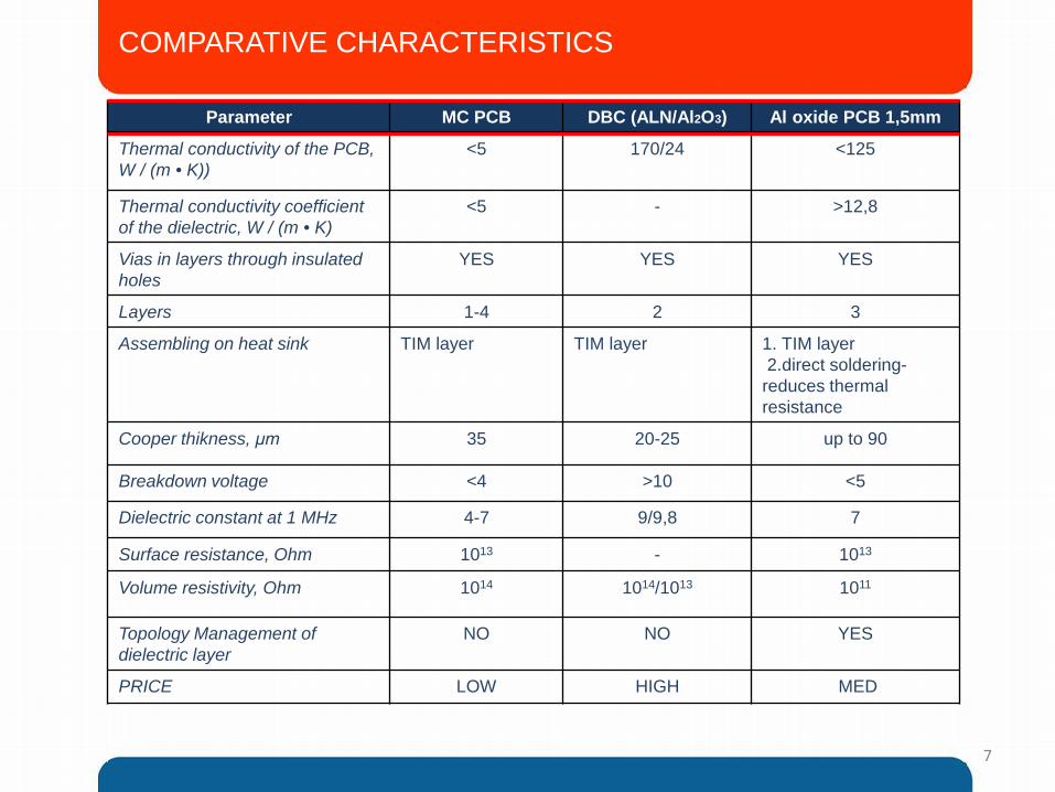
Parameter MC PCB DBC (ALN/Al2O3) Al oxide PCB 1,5mm
Thermal conductivity of the PCB, W / (m • K))
<5 170/24 <125
Thermal conductivity coefficient of the dielectric, W / (m • K)
<5 - >12,8
Vias in layers through insulated holes
YES YES YES
Layers 1-4 2 3
Assembling on heat sink TIM layer TIM layer 1. TIM layer 2.direct soldering-reduces thermal resistance
Cooper thikness, μm 35 20-25 up to 90
Breakdown voltage <4 >10 <5
Dielectric constant at 1 MHz 4-7 9/9,8 7
Surface resistance, Ohm 1013 - 1013
Volume resistivity, Ohm 1014 1014/1013
1011
Topology Management of dielectric layer
NO NO YES
PRICE LOW HIGH MED
COMPARATIVE CHARACTERISTICS
7
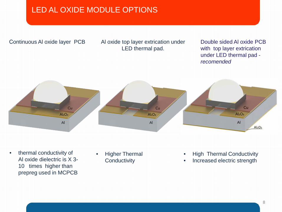
Double sided Al oxide PCB with top layer extrication under LED thermal pad -recomended
Сontinuous Al oxide layer PCB Al oxide top layer extrication under LED thermal pad.
• High Thermal Conductivity • Increased electric strength
• Higher Thermal Conductivity
• thermal conductivity of Al oxide dielectric is X 3-10 times higher than prepreg used in MCPCB
LED AL OXIDE MODULE OPTIONS
8
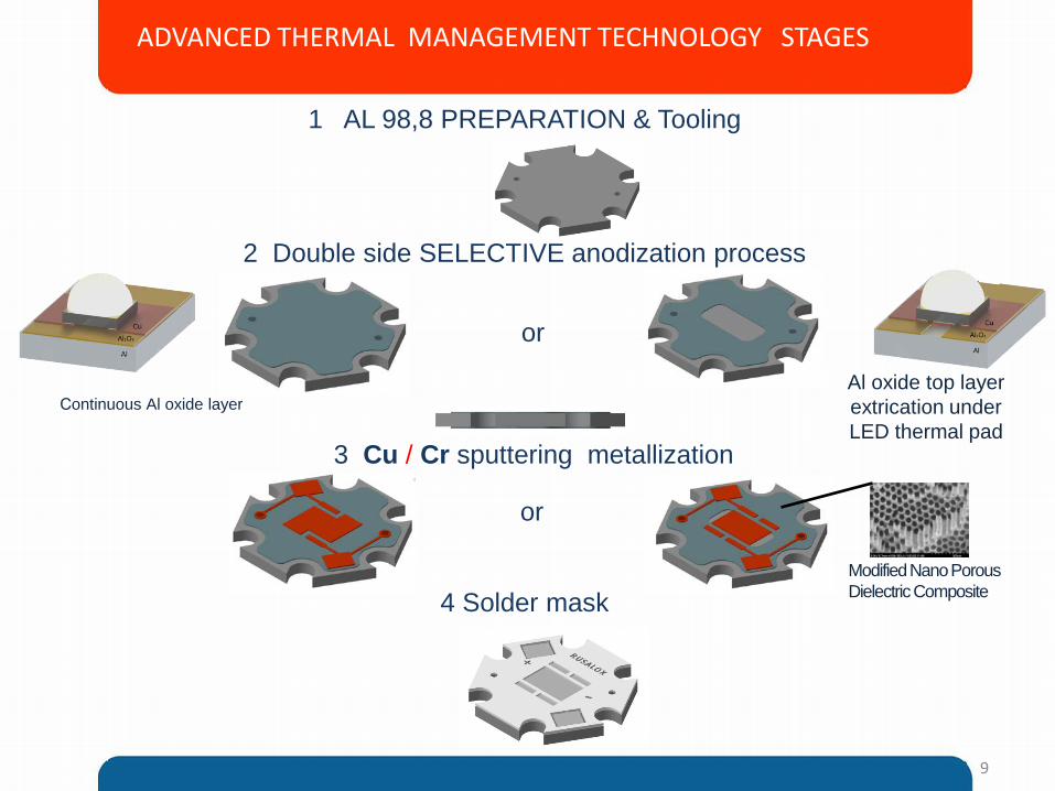
ADVANCED THERMAL MANAGEMENT TECHNOLOGY STAGES
9
2 Double side SELECTIVE anodization process
3 Cu / Cr sputtering metallization
4 Solder mask
1 AL 98,8 PREPARATION & Tooling
or
or
Al oxide top layer extrication under LED thermal pad
Сontinuous Al oxide layer
Modified Nano Porous Dielectric Composite
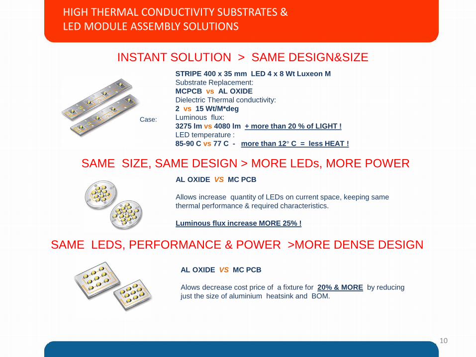
STRIPE 400 x 35 mm LED 4 x 8 Wt Luxeon M Substrate Replacement: MCPCB vs AL OXIDE Dielectric Thermal conductivity: 2 vs 15 Wt/M*deg Luminous flux: 3275 lm vs 4080 lm + more than 20 % of LIGHT ! LED temperature : 85-90 C vs 77 C - more than 12° C = less HEAT !
10
INSTANT SOLUTION > SAME DESIGN&SIZE
SAME SIZE, SAME DESIGN > MORE LEDs, MORE POWER
Case:
AL OXIDE VS MC PCB Allows increase quantity of LEDs on current space, keeping same thermal performance & required characteristics. Luminous flux increase MORE 25% !
SAME LEDS, PERFORMANCE & POWER >MORE DENSE DESIGN
AL OXIDE VS MC PCB Alows decrease cost price of a fixture for 20% & MORE by reducing just the size of aluminium heatsink and BOM.
HIGH THERMAL CONDUCTIVITY SUBSTRATES & LED MODULE ASSEMBLY SOLUTIONS
11
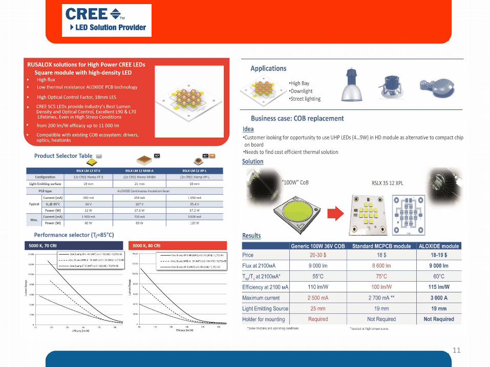
12
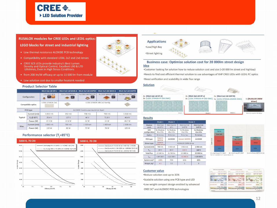
13
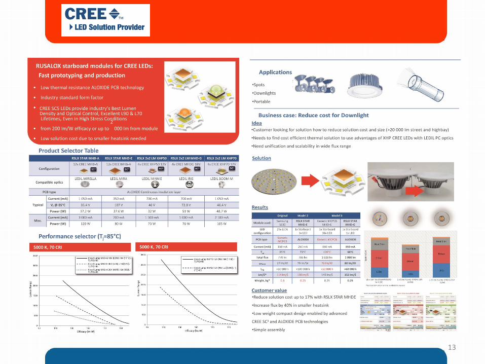
HIGH THERMAL CONDUCTIVITY PCB AL OXIDE TECHNOLOGY
POSSIBLE APPLICATIONS OVERVIEW
14
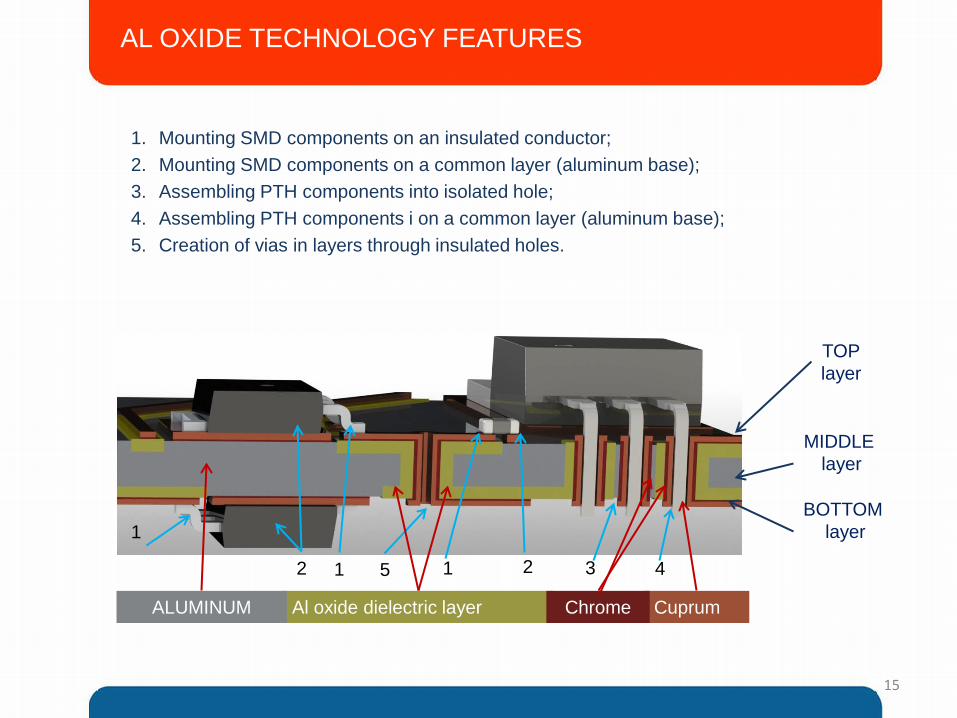
AL OXIDE TECHNOLOGY FEATURES
1. Mounting SMD components on an insulated conductor; 2. Mounting SMD components on a common layer (aluminum base); 3. Assembling PTH components into isolated hole; 4. Assembling PTH components i on a common layer (aluminum base); 5. Creation of vias in layers through insulated holes.
TOP layer
Al oxide dielectric layer
BOTTOM layer
5 1 2 3 4 2
MIDDLE layer
Cuprum Chrome ALUMINUM
1
1
15
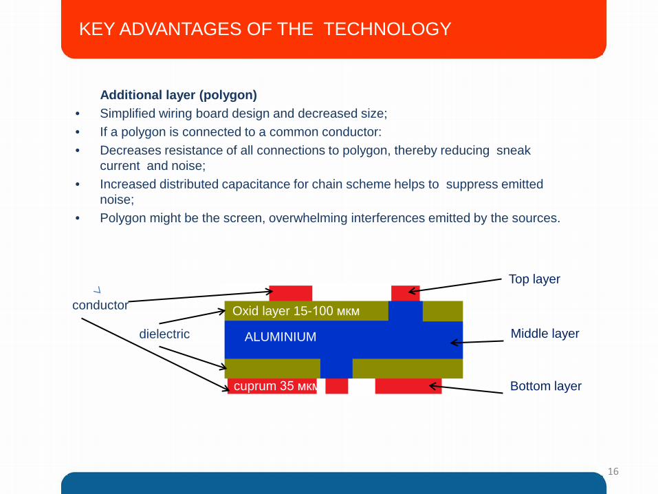
KEY ADVANTAGES OF THE TECHNOLOGY
Additional layer (polygon) • Simplified wiring board design and decreased size; • If a polygon is connected to a common conductor: • Decreases resistance of all connections to polygon, thereby reducing sneak
current and noise; • Increased distributed capacitance for chain scheme helps to suppress emitted
noise; • Polygon might be the screen, overwhelming interferences emitted by the sources.
Oxid layer 15-100 мкм
ALUMINIUM
cuprum 35 мкм
Top layer
Middle layer
Bottom layer
dielectric
conductor
16
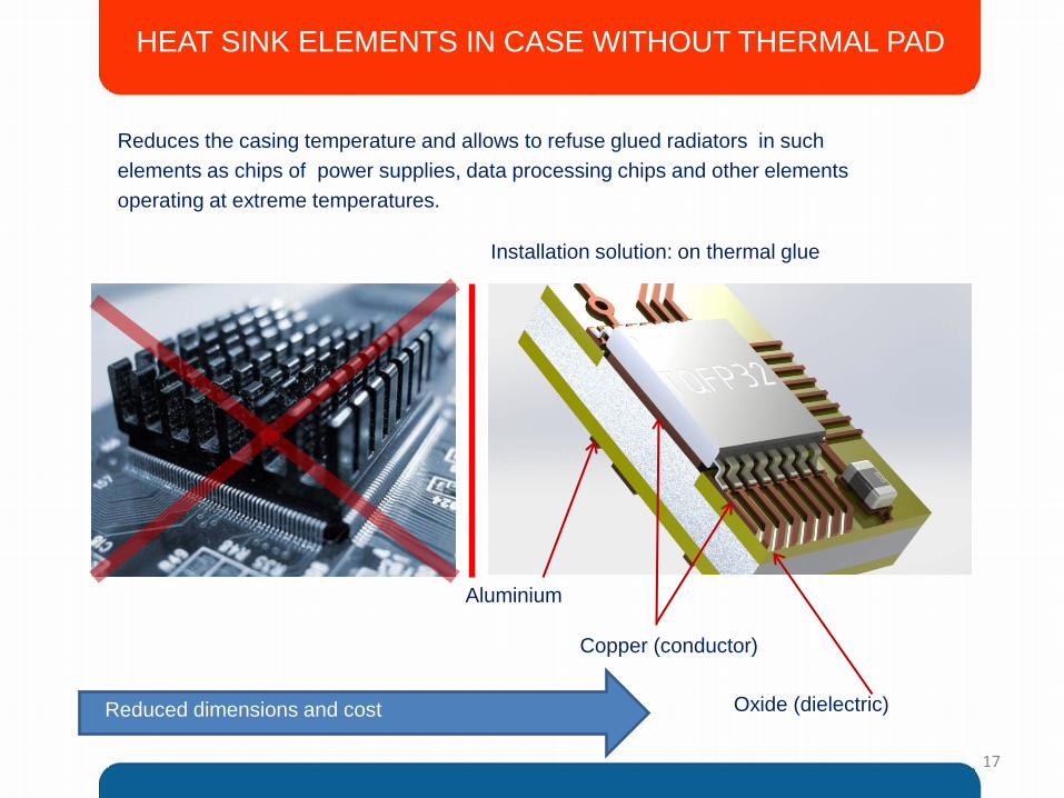
Reduces the casing temperature and allows to refuse glued radiators in such elements as chips of power supplies, data processing chips and other elements operating at extreme temperatures.
Reduced dimensions and cost
Installation solution: on thermal glue
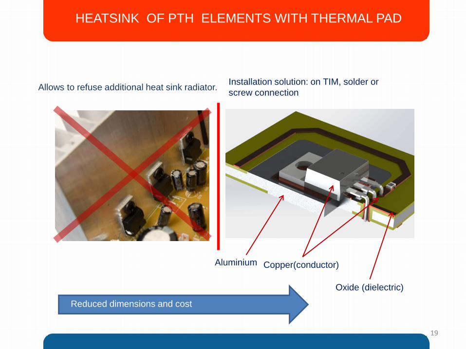
Aluminium
Oxide (dielectric)
Copper (conductor)
HEAT SINK ELEMENTS IN CASE WITHOUT THERMAL PAD
17
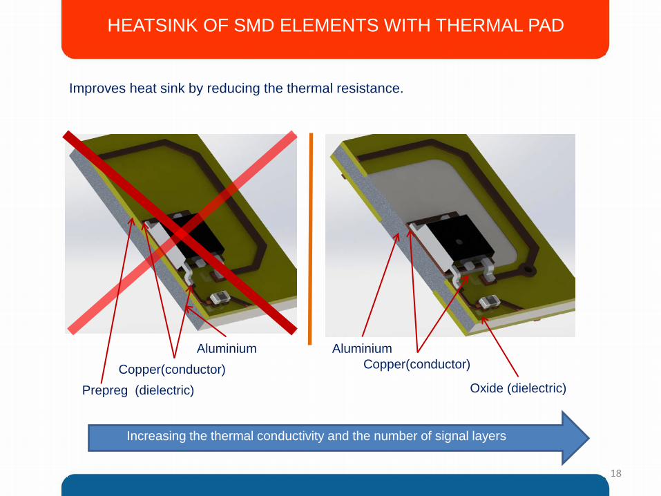
Improves heat sink by reducing the thermal resistance.
Increasing the thermal conductivity and the number of signal layers
Oxide (dielectric)
Copper(conductor) Aluminium
Prepreg (dielectric) Copper(conductor)
HEATSINK OF SMD ELEMENTS WITH THERMAL PAD
Aluminium
18
Aluminium
Oxide (dielectric)
Copper(conductor)
Installation solution: on TIM, solder or screw connection
HEATSINK OF PTH ELEMENTS WITH THERMAL PAD
Reduced dimensions and cost
Allows to refuse additional heat sink radiator.
19
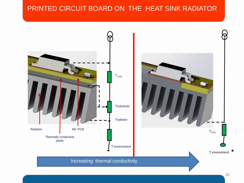
Increasing thermal conductivity
Т environment
Тbody
Т body
Тsubstrate
Тradiator
Thermally conductive paste
Radiator MC PCB
PRINTED CIRCUIT BOARD ON THE HEAT SINK RADIATOR
Т environment
20
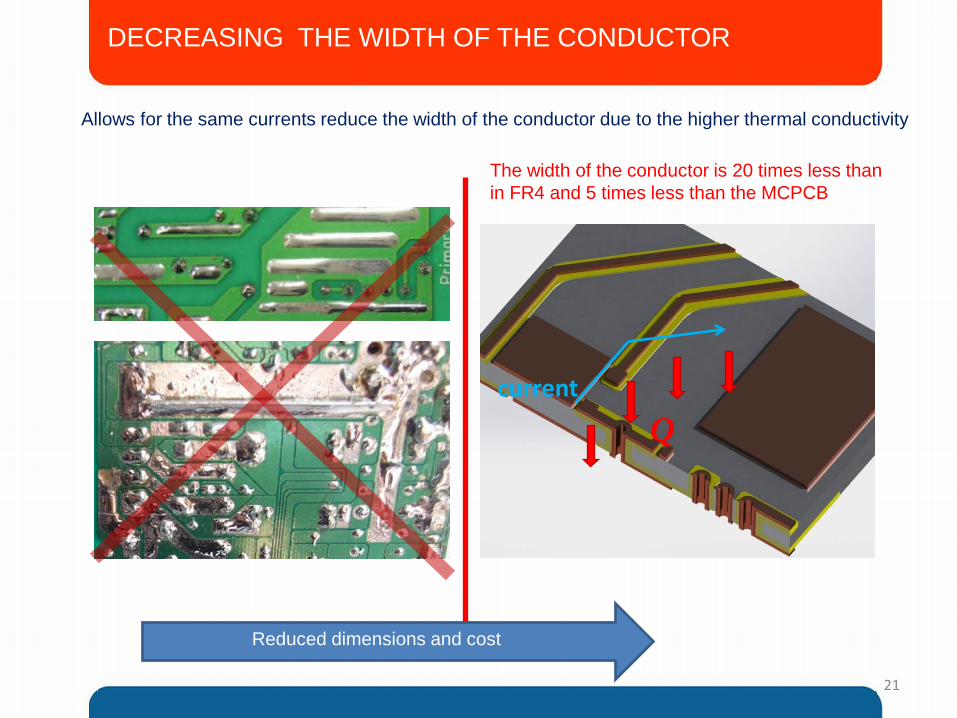
Reduced dimensions and cost
The width of the conductor is 20 times less than in FR4 and 5 times less than the MCPCB
Q current
DECREASING THE WIDTH OF THE CONDUCTOR
Allows for the same currents reduce the width of the conductor due to the higher thermal conductivity
21
RELIABILITY
Highest reliability is one the most important key attributes of ALOXIDE technology and products. ALOXIDE based products, substrates and packages, demonstrate the highest reliability standards required in the semiconductor electronics packaging. All ALOXIDE PCB and LE passed successfully extensive reliability tests. Tests were done according to the most stringent requirements commonly used in the industry. Thermal cycling – substrates and assemblies passed numerous and extensive thermal cycling tests, and reached repeatedly over 1,000 cycles and also (when tested to this level) 3,000 cycles between -55 to +125 ℃, without failure. HAST tests for molded devices Mechanical vibration tests for assemblies X-ray analysis following preconditioning and soldering processes HTHH tests: Yield degradation following high Temperature and high Humidity preconditioning and high and low temperature storage Via chain resistance stability Adhesion and delamination tests
22
23
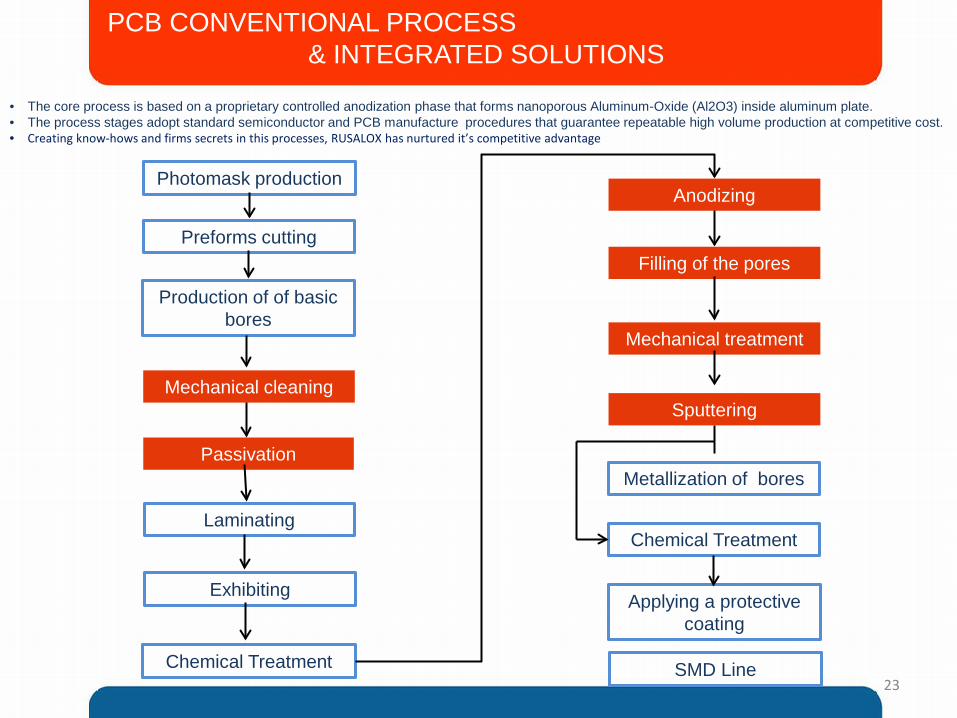
PCB CONVENTIONAL PROCESS & INTEGRATED SOLUTIONS
• The core process is based on a proprietary controlled anodization phase that forms nanoporous Aluminum-Oxide (Al2O3) inside aluminum plate. • The process stages adopt standard semiconductor and PCB manufacture procedures that guarantee repeatable high volume production at competitive cost. • Creating know-hows and firms secrets in this processes, RUSALOX has nurtured it’s competitive advantage
Mechanical cleaning
Passivation
Filling of the pores
Mechanical treatment
Anodizing Photomask production
Preforms cutting
Production of of basic bores
Laminating
Exhibiting
Chemical Treatment
Metallization of bores
Chemical Treatment
Applying a protective coating
Sputtering
SMD Line
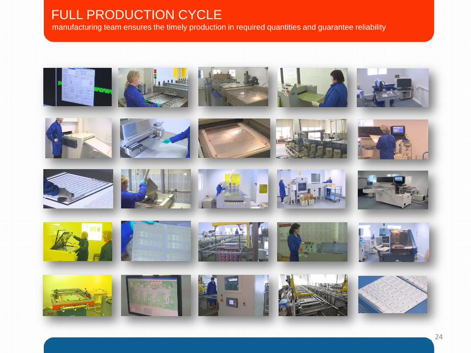
FULL PRODUCTION CYCLE manufacturing team ensures the timely production in required quantities and guarantee reliability
24
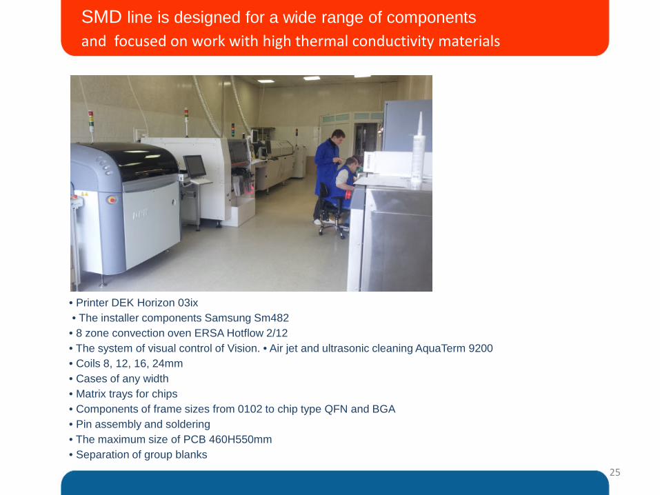
SMD line is designed for a wide range of components and focused on work with high thermal conductivity materials
• Printer DEK Horizon 03ix • The installer components Samsung Sm482 • 8 zone convection oven ERSA Hotflow 2/12 • The system of visual control of Vision. • Air jet and ultrasonic cleaning AquaTerm 9200 • Coils 8, 12, 16, 24mm • Cases of any width • Matrix trays for chips • Components of frame sizes from 0102 to chip type QFN and BGA • Pin assembly and soldering • The maximum size of PCB 460H550mm • Separation of group blanks
25
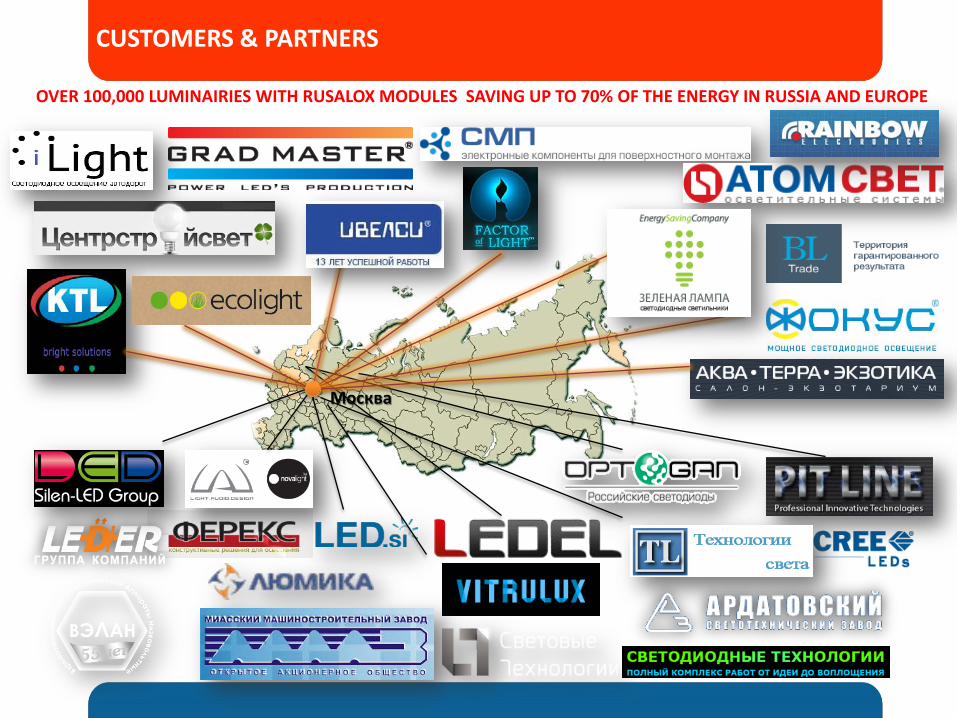
CUSTOMERS & PARTNERS
Москва
OVER 100,000 LUMINAIRIES WITH RUSALOX MODULES SAVING UP TO 70% OF THE ENERGY IN RUSSIA AND EUROPE
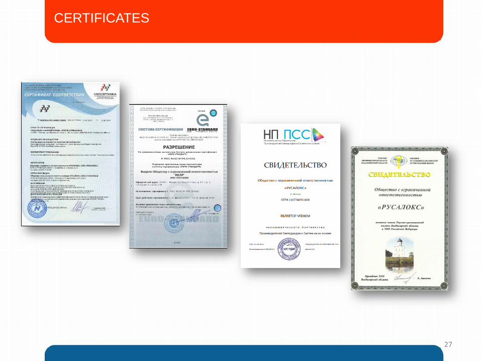
CERTIFICATES
27
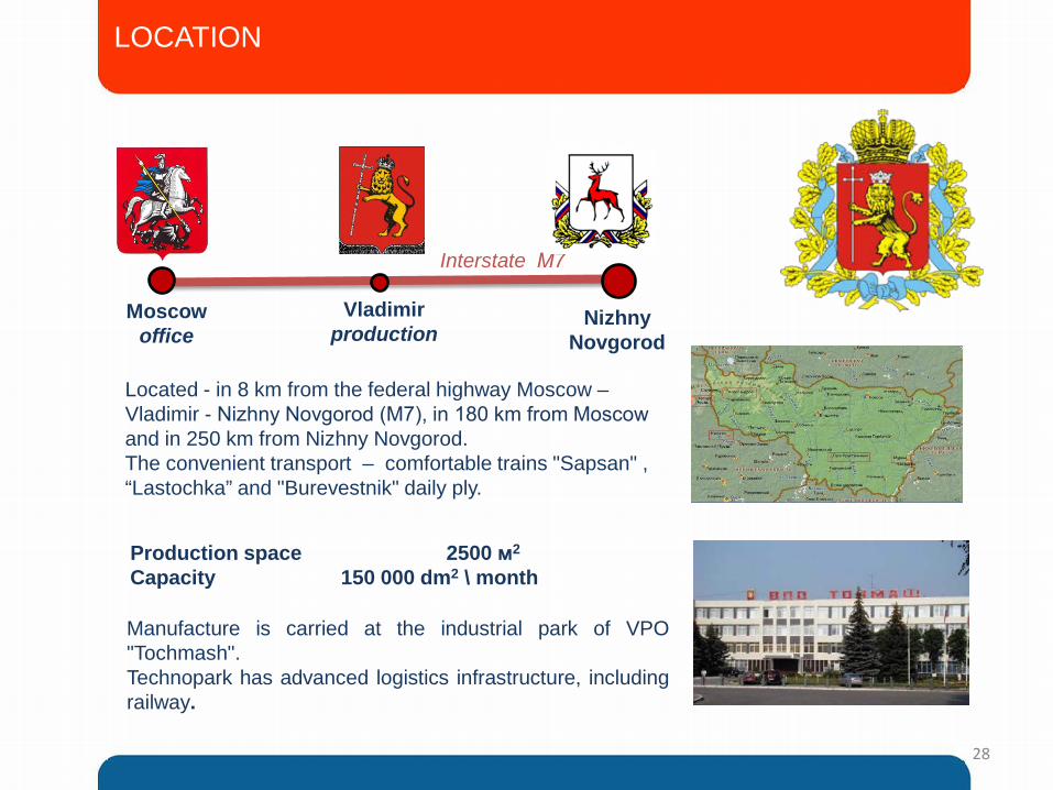
Manufacture is carried at the industrial park of VPO "Tochmash". Technopark has advanced logistics infrastructure, including railway.
Production space 2500 м2
Capacity 150 000 dm2 \ month
Nizhny Novgorod
Vladimir production
Moscow office
Interstate М7
Located - in 8 km from the federal highway Moscow – Vladimir - Nizhny Novgorod (М7), in 180 km from Moscow and in 250 km from Nizhny Novgorod. The convenient transport – comfortable trains "Sapsan" , “Lastochka” and "Burevestnik" daily ply.
LOCATION
28
.
29
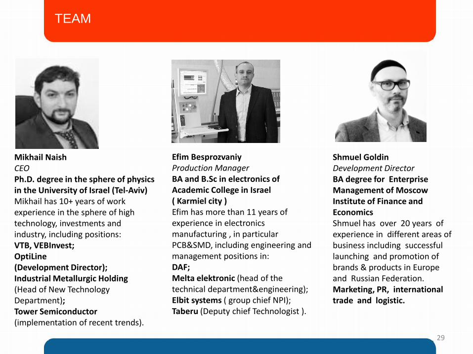
Shmuel Goldin Development Director BA degree for Enterprise Management of Moscow Institute of Finance and Economics Shmuel has over 20 years of experience in different areas of business including successful launching and promotion of brands & products in Europe and Russian Federation. Marketing, PR, international trade and logistic.
Mikhail Naish CEO Ph.D. degree in the sphere of physics in the University of Israel (Tel-Aviv) Mikhail has 10+ years of work experience in the sphere of high technology, investments and industry, including positions: VTB, VEBInvest; OptiLine (Development Director); Industrial Metallurgic Holding (Head of New Technology Department); Tower Semiconductor (implementation of recent trends).
Efim Besprozvaniy Production Manager BA and B.Sc in electronics of Academic College in Israel ( Karmiel city ) Efim has more than 11 years of experience in electronics manufacturing , in particular PCB&SMD, including engineering and management positions in: DAF; Melta elektronic (head of the technical department&engineering); Elbit systems ( group chief NPI); Taberu (Deputy chief Technologist ).
TEAM