Embed Size (px)
Citation preview

High Voltage Latch-Up Proof, Quad SPST Switches
Data Sheet ADG5412/ADG5413
Rev. D Document Feedback Information furnished by Analog Devices is believed to be accurate and reliable. However, no responsibility is assumed by Analog Devices for its use, nor for any infringements of patents or other rights of third parties that may result from its use. Specifications subject to change without notice. No license is granted by implication or otherwise under any patent or patent rights of Analog Devices. Trademarks and registered trademarks are the property of their respective owners.
One Technology Way, P.O. Box 9106, Norwood, MA 02062-9106, U.S.A. Tel: 781.329.4700 ©2010–2017 Analog Devices, Inc. All rights reserved. Technical Support www.analog.com
FEATURES Latch-up proof 8 kV human body model (HBM) ESD rating Low on resistance (<10 Ω) ±9 V to ±22 V dual-supply operation 9 V to 40 V single-supply operation 48 V supply maximum ratings Fully specified at ±15 V, ±20 V, +12 V, and +36 V VSS to VDD analog signal range
APPLICATIONS Relay replacement Automatic test equipment Data acquisition Instrumentation Avionics Audio and video switching Communication systems
FUNCTIONAL BLOCK DIAGRAMS
IN1
S1
D1
IN2
S2
D2
IN3
S3
D3
IN4
S4
D4
ADG5412
SWITCHES SHOWN FOR A LOGIC 1 INPUT.
IN2
S2
D2
IN3
S3
D3
IN1
S1
D1
IN4
S4
D4
ADG5413
0920
2-00
1
Figure 1.
GENERAL DESCRIPTION The ADG5412/ADG5413 contain four independent single-pole/ single-throw (SPST) switches. The ADG5412 switches turn on with Logic 1. The ADG5413 has two switches with digital control logic similar to that of the ADG5412; however, the logic is inverted on the other two switches. Each switch conducts equally well in both directions when on, and each switch has an input signal range that extends to the supplies. In the off condition, signal levels up to the supplies are blocked.
The ADG5412 and ADG5413 do not have a VL pin. The digital inputs are compatible with 3 V logic inputs over the full operating supply range.
The on-resistance profile is very flat over the full analog input range, which ensures good linearity and low distortion when switching audio signals. High switching speed also makes the devices suitable for video signal switching. The ADG5413 exhibits break-before-make switching action for use in multiplexer applications.
PRODUCT HIGHLIGHTS 1. Trench isolation guards against latch-up. A dielectric trench
separates the P and N channel transistors thereby preventing latch-up even under severe overvoltage conditions.
2. Low RON. 3. Dual-supply operation. For applications where the analog
signal is bipolar, the ADG5412/ADG5413 can be operated from dual supplies up to ±22 V.
4. Single-supply operation. For applications where the analog signal is unipolar, the ADG5412/ADG5413 can be operated from a single rail power supply up to 40 V.
5. 3 V logic compatible digital inputs: VINH = 2.0 V, VINL = 0.8 V. 6. No VL logic power supply required.

ADG5412/ADG5413 Data Sheet
Rev. D | Page 2 of 19
TABLE OF CONTENTS Features .............................................................................................. 1 Applications ....................................................................................... 1 Functional Block Diagrams ............................................................. 1 General Description ......................................................................... 1 Product Highlights ........................................................................... 1 Revision History ............................................................................... 2 Specifications ..................................................................................... 3
±15 V Dual Supply ....................................................................... 3 ±20 V Dual Supply ....................................................................... 4 12 V Single Supply ........................................................................ 5 36 V Single Supply ........................................................................ 6
Continuous Current per Channel, Sx or Dx ..............................7 Absolute Maximum Ratings ............................................................8
ESD Caution...................................................................................8 Pin Configurations and Function Descriptions ............................9 Typical Performance Characteristics ........................................... 10 Test Circuits ..................................................................................... 14 Terminology .................................................................................... 16 Trench Isolation .............................................................................. 17 Applications Information .............................................................. 18 Outline Dimensions ....................................................................... 19
Ordering Guide .......................................................................... 19
REVISION HISTORY 11/2017—Rev. C to Rev. D Change to Source Off Leakage, IS (Off) Parameter and Drain Off Leakage, ID (Off) Parameter, Table 1 ....................................... 3 Change to Source Off Leakage, IS (Off) Parameter and Drain Off Leakage, ID (Off) Parameter, Table 2 ....................................... 4 Change to Source Off Leakage, IS (Off) Parameter and Drain Off Leakage, ID (Off) Parameter, Table 3 ....................................... 5 Change to Source Off Leakage, IS (Off) Parameter and Drain Off Leakage, ID (Off) Parameter, Table 4 ....................................... 6 Updated Outline Dimensions ....................................................... 19 Changes to Ordering Guide .......................................................... 19 5/2016—Rev. B to Rev. C Changes to Off Isolation Parameter, Table 1 ................................. 3 Changes to Off Isolation Parameter, Table 2 ................................. 4 Changes to Off Isolation Parameter, Table 3 ................................. 6 Changes to Off Isolation Parameter, Table 4 ................................. 7 Changes to Figure 2, Figure 3, and Table 7 ................................... 9 9/2015—Rev. A to Rev. B Changes to Figure 3 .......................................................................... 9 Change to Figure 20 ....................................................................... 12 Change to Application Information Section ............................... 18 6/2011—Rev. 0 to Rev. A Change to ISS Parameter in Table 2 ................................................. 4 7/2010—Revision 0: Initial Version

Data Sheet ADG5412/ADG5413
Rev. D | Page 3 of 19
SPECIFICATIONS ±15 V DUAL SUPPLY VDD = +15 V ± 10%, VSS = −15 V ± 10%, GND = 0 V, unless otherwise noted.
Table 1. Parameter +25°C −40°C to +85°C −40°C to +125°C Unit Test Conditions/Comments ANALOG SWITCH
Analog Signal Range VDD to VSS V On Resistance, RON 9.8 Ω typ VS = ±10 V, IS = −10 mA;
see Figure 24 11 14 16 Ω max VDD = +13.5 V, VSS = −13.5 V On-Resistance Match Between Channels,
∆RON 0.35 Ω typ VS = ±10 V, IS = −10 mA
0.7 0.9 1.1 Ω max On-Resistance Flatness, RFLAT (ON) 1.2 Ω typ VS = ±10 V, IS = −10 mA
1.6 2 2.2 Ω max LEAKAGE CURRENTS VDD = +16.5 V, VSS = −16.5 V
Source Off Leakage, IS (Off ) ±0.05 nA typ VS = ±10 V, VD = 10 V; see Figure 27
±0.25 ±0.75 ±6 nA max Drain Off Leakage, ID (Off ) ±0.05 nA typ VS = ±10 V, VD = 10 V;
see Figure 27 ±0.25 ±0.75 ±6 nA max Channel On Leakage, ID (On), IS (On) ±0.1 nA typ VS = VD = ±10 V; see Figure 23
±0.4 ±2 ±12 nA max DIGITAL INPUTS
Input High Voltage, VINH 2.0 V min Input Low Voltage, VINL 0.8 V max Input Current, IINL or IINH 0.002 µA typ VIN = VGND or VDD ±0.1 µA max Digital Input Capacitance, CIN 2.5 pF typ
DYNAMIC CHARACTERISTICS1 tON 170 ns typ RL = 300 Ω, CL = 35 pF 202 236 262 ns max VS = 10 V; see Figure 31 tOFF 120 ns typ RL = 300 Ω, CL = 35 pF 145 170 182 ns max VS = 10 V; see Figure 31 Break-Before-Make Time Delay, tD
(ADG5413 Only) 15 ns typ RL = 300 Ω, CL = 35 pF
6 ns min VS1 = VS2 = 10 V; see Figure 30 Charge Injection, QINJ 240 pC typ VS = 0 V, RS = 0 Ω, CL = 1 nF;
see Figure 32 Off Isolation −78 dB typ RL = 50 Ω, CL = 5 pF,
f = 100 kHz; see Figure 26 Channel-to-Channel Crosstalk −70 dB typ RL = 50 Ω, CL = 5 pF, f = 1 MHz;
see Figure 25 Total Harmonic Distortion + Noise 0.009 % typ RL = 1 kΩ, 15 V p-p, f = 20 Hz
to 20 kHz; see Figure 28 −3 dB Bandwidth 167 MHz typ RL = 50 Ω, CL = 5 pF; see
Figure 29 Insertion Loss −0.7 dB typ RL = 50 Ω, CL = 5 pF, f = 1 MHz;
see Figure 29 CS (Off ) 18 pF typ VS = 0 V, f = 1 MHz CD (Off ) 18 pF typ VS = 0 V, f = 1 MHz CD (On), CS (On) 60 pF typ VS = 0 V, f = 1 MHz

ADG5412/ADG5413 Data Sheet
Rev. D | Page 4 of 19
Parameter +25°C −40°C to +85°C −40°C to +125°C Unit Test Conditions/Comments POWER REQUIREMENTS VDD = +16.5 V, VSS = −16.5 V
IDD 45 µA typ Digital inputs = 0 V or VDD 55 70 µA max ISS 0.001 µA typ Digital inputs = 0 V or VDD 1 µA max VDD/VSS ±9/±22 V min/V max GND = 0 V
1 Guaranteed by design; not subject to production test.
±20 V DUAL SUPPLY VDD = +20 V ± 10%, VSS = −20 V ± 10%, GND = 0 V, unless otherwise noted.
Table 2. Parameter +25°C −40°C to +85°C −40°C to +125°C Unit Test Conditions/Comments ANALOG SWITCH
Analog Signal Range VDD to VSS V On Resistance, RON 9 Ω typ VS = ±15 V, IS = −10 mA;
see Figure 24 10 13 15 Ω max VDD = +18 V, VSS = −18 V On-Resistance Match Between
Channels, ∆RON 0.35 Ω typ VS = ±15 V, IS = −10 mA
0.7 0.9 1.1 Ω max On-Resistance Flatness, RFLAT (ON) 1.5 Ω typ VS = ±15 V, IS = −10 mA
1.8 2.2 2.5 Ω max LEAKAGE CURRENTS VDD = +22 V, VSS = −22 V
Source Off Leakage, IS (Off ) ±0.05 nA typ VS = ±15 V, VD = 15 V; see Figure 27
±0.25 ±0.75 ±6 nA max Drain Off Leakage, ID (Off ) ±0.05 nA typ VS = ±15 V, VD = 15 V;
see Figure 27 ±0.25 ±0.75 ±6 nA max Channel On Leakage, ID (On), IS (On) ±0.1 nA typ VS = VD = ±15 V; see
Figure 23 ±0.4 ±2 ±12 nA max
DIGITAL INPUTS Input High Voltage, VINH 2.0 V min Input Low Voltage, VINL 0.8 V max Input Current, IINL or IINH 0.002 µA typ VIN = VGND or VDD ±0.1 µA max Digital Input Capacitance, CIN 2.5 pF typ
DYNAMIC CHARACTERISTICS1 tON 158 ns typ RL = 300 Ω, CL = 35 pF 187 217 240 ns max VS = 10 V; see Figure 31 tOFF 110 ns typ RL = 300 Ω, CL = 35 pF 138 154 170 ns max VS = 10 V; see Figure 31 Break-Before-Make Time Delay, tD
(ADG5413 Only) 12 ns typ RL = 300 Ω, CL = 35 pF
5 ns min VS1 = VS2 = 10 V; see Figure 30
Charge Injection, QINJ 310 pC typ VS = 0 V, RS = 0 Ω, CL = 1 nF; see Figure 32
Off Isolation −78 dB typ RL = 50 Ω, CL = 5 pF, f = 100 kHz; see Figure 26
Channel-to-Channel Crosstalk −70 dB typ RL = 50 Ω, CL = 5 pF, f = 1 MHz; see Figure 25

Data Sheet ADG5412/ADG5413
Rev. D | Page 5 of 19
Parameter +25°C −40°C to +85°C −40°C to +125°C Unit Test Conditions/Comments Total Harmonic Distortion + Noise 0.007 % typ RL = 1 kΩ, 20 V p-p, f = 20 Hz to
20 kHz; see Figure 28 −3 dB Bandwidth 160 MHz typ RL = 50 Ω, CL = 5 pF;
see Figure 29 Insertion Loss −0.6 dB typ RL = 50 Ω, CL = 5 pF, f = 1 MHz;
see Figure 29 CS (Off ) 17 pF typ VS = 0 V, f = 1 MHz CD (Off ) 17 pF typ VS = 0 V, f = 1 MHz CD (On), CS (On) 60 pF typ VS = 0 V, f = 1 MHz
POWER REQUIREMENTS VDD = +22 V, VSS = −22 V IDD 50 µA typ Digital inputs = 0 V or VDD 70 110 µA max ISS 0.001 µA typ Digital inputs = 0 V or VDD 1 µA max VDD/VSS ±9/±22 V min/V max GND = 0 V
1 Guaranteed by design; not subject to production test.
12 V SINGLE SUPPLY VDD = 12 V ± 10%, VSS = 0 V, GND = 0 V, unless otherwise noted.
Table 3. Parameter +25°C −40°C to +85°C −40°C to +125°C Unit Test Conditions/Comments ANALOG SWITCH
Analog Signal Range 0 V to VDD V On Resistance, RON 19 Ω typ VS = 0 V to 10 V, IS = −10 mA;
see Figure 24 22 27 31 Ω max VDD = 10.8 V, VSS = 0 V On-Resistance Match Between Channels,
∆RON 0.4 Ω typ VS = 0 V to 10 V, IS = −10 mA
0.8 1 1.2 Ω max On-Resistance Flatness, RFLAT (ON) 4.4 Ω typ VS = 0 V to 10 V, IS = −10 mA
5.5 6.5 7.5 Ω max LEAKAGE CURRENTS VDD = 13.2 V, VSS = 0 V
Source Off Leakage, IS (Off ) ±0.05 nA typ VS = 1 V/10 V, VD = 10 V/1 V; see Figure 27
±0.25 ±0.75 ±6 nA max Drain Off Leakage, ID (Off ) ±0.05 nA typ VS = 1 V/10 V, VD = 10 V/1 V;
see Figure 27 ±0.25 ±0.75 ±6 nA max Channel On Leakage, ID (On), IS (On) ±0.1 nA typ VS = VD = 1 V/10 V; see
Figure 23 ±0.4 ±2 ±12 nA max DIGITAL INPUTS
Input High Voltage, VINH 2.0 V min Input Low Voltage, VINL 0.8 V max Input Current, IINL or IINH 0.002 µA typ VIN = VGND or VDD ±0.1 µA max Digital Input Capacitance, CIN 2.5 pF typ
DYNAMIC CHARACTERISTICS1 tON 225 ns typ RL = 300 Ω, CL = 35 pF 296 358 403 ns max VS = 8 V; see Figure 31 tOFF 150 ns typ RL = 300 Ω, CL = 35 pF 187 222 247 ns max VS = 8 V; see Figure 31

ADG5412/ADG5413 Data Sheet
Rev. D | Page 6 of 19
Parameter +25°C −40°C to +85°C −40°C to +125°C Unit Test Conditions/Comments Break-Before-Make Time Delay, tD
(ADG5413 Only) 70 ns typ RL = 300 Ω, CL = 35 pF
38 ns min VS1 = VS2 = 8 V; see Figure 30 Charge Injection, QINJ 95 pC typ VS = 6 V, RS = 0 Ω, CL = 1 nF;
see Figure 32 Off Isolation −78 dB typ RL = 50 Ω, CL = 5 pF,
f = 100 kHz; see Figure 26 Channel-to-Channel Crosstalk −70 dB typ RL = 50 Ω, CL = 5 pF, f = 1 MHz;
see Figure 25 Total Harmonic Distortion + Noise 0.07 % typ RL = 1 kΩ, 6 V p-p, f = 20 Hz
to 20 kHz; see Figure 28 −3 dB Bandwidth 180 MHz typ RL = 50 Ω, CL = 5 pF; see
Figure 29 Insertion Loss −1.3 dB typ RL = 50 Ω, CL = 5 pF, f = 1 MHz;
see Figure 29 CS (Off ) 22 pF typ VS = 6 V, f = 1 MHz CD (Off ) 22 pF typ VS = 6 V, f = 1 MHz CD (On), CS (On) 58 pF typ VS = 6 V, f = 1 MHz
POWER REQUIREMENTS VDD = 13.2 V IDD 40 µA typ Digital inputs = 0 V or VDD 65 µA max VDD 9/40 V min/V max GND = 0 V, VSS = 0 V
1 Guaranteed by design; not subject to production test.
36 V SINGLE SUPPLY VDD = 36 V ± 10%, VSS = 0 V, GND = 0 V, unless otherwise noted.
Table 4. Parameter +25°C −40°C to +85°C −40°C to +125°C Unit Test Conditions/Comments ANALOG SWITCH
Analog Signal Range 0 V to VDD V On Resistance, RON 10.6 Ω typ VS = 0 V to 30 V, IS = −10 mA;
see Figure 24 12 15 17 Ω max VDD = 32.4 V, VSS = 0 V On-Resistance Match Between Channels,
∆RON 0.35 Ω typ VS = 0 V to 30 V, IS = −10 mA
0.7 0.9 1.1 Ω max On-Resistance Flatness, RFLAT(ON) 2.7 Ω typ VS = 0 V to 30 V, IS = −10 mA
3.2 3.8 4.5 Ω max LEAKAGE CURRENTS VDD = 39.6 V, VSS = 0 V
Source Off Leakage, IS (Off ) ±0.05 nA typ VS = 1 V/30 V, VD = 30 V/1 V; see Figure 27
±0.25 ±0.75 ±6 nA max Drain Off Leakage, ID (Off ) ±0.05 nA typ VS = 1 V/30 V, VD = 30 V/1 V;
see Figure 27 ±0.25 ±0.75 ±6 nA max Channel On Leakage, ID (On), IS (On) ±0.1 nA typ VS = VD = 1 V/30 V; see
Figure 23 ±0.4 ±2 ±12 nA max
Data Sheet ADG5412/ADG5413
Rev. D | Page 7 of 19
Parameter +25°C −40°C to +85°C −40°C to +125°C Unit Test Conditions/Comments DIGITAL INPUTS
Input High Voltage, VINH 2.0 V min Input Low Voltage, VINL 0.8 V max Input Current, IINL or IINH 0.002 µA typ VIN = VGND or VDD ±0.1 µA max Digital Input Capacitance, CIN 2.5 pF typ
DYNAMIC CHARACTERISTICS1 tON 180 ns typ RL = 300 Ω, CL = 35 pF 220 230 248 ns max VS = 18 V; see Figure 31 tOFF 130 ns typ RL = 300 Ω, CL = 35 pF
169 167 174 ns max VS = 18 V; see Figure 31 Break-Before-Make Time Delay, tD
(ADG5413 Only) 25 ns typ RL = 300 Ω, CL = 35 pF
8 ns min VS1 = VS2 = 18 V; see Figure 30 Charge Injection, QINJ 280 pC typ VS = 18 V, RS = 0 Ω, CL = 1 nF;
see Figure 32 Off Isolation −78 dB typ RL = 50 Ω, CL = 5 pF,
f = 100 kHz; see Figure 26 Channel-to-Channel Crosstalk −70 dB typ RL = 50 Ω, CL = 5 pF, f = 1 MHz;
Figure 25 Total Harmonic Distortion + Noise 0.03 % typ RL = 1 kΩ, 18 V p-p, f = 20 Hz
to 20 kHz; see Figure 28 −3 dB Bandwidth 174 MHz typ RL = 50 Ω, CL = 5 pF; see
Figure 29 Insertion Loss −0.8 dB typ RL = 50 Ω, CL = 5 pF, f = 1 MHz;
see Figure 29 CS (Off ) 18 pF typ VS = 18 V, f = 1 MHz CD (Off ) 18 pF typ VS = 18 V, f = 1 MHz CD (On), CS (On) 58 pF typ VS = 18 V, f = 1 MHz
POWER REQUIREMENTS VDD = 39.6 V IDD 80 µA typ Digital inputs = 0 V or VDD 100 130 µA max VDD 9/40 V min/V max GND = 0 V, VSS = 0 V
1 Guaranteed by design; not subject to production test.
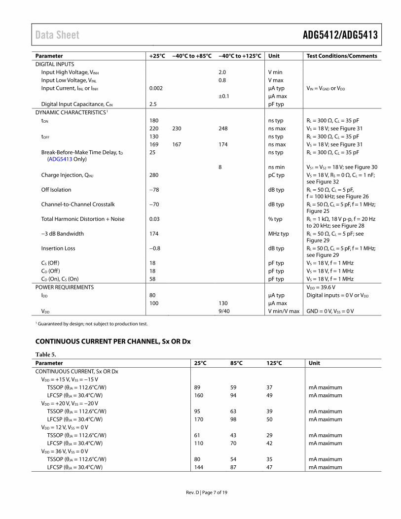
CONTINUOUS CURRENT PER CHANNEL, Sx OR Dx
Table 5. Parameter 25°C 85°C 125°C Unit CONTINUOUS CURRENT, Sx OR Dx
VDD = +15 V, VSS = −15 V TSSOP (θJA = 112.6°C/W) 89 59 37 mA maximum LFCSP (θJA = 30.4°C/W) 160 94 49 mA maximum
VDD = +20 V, VSS = −20 V TSSOP (θJA = 112.6°C/W) 95 63 39 mA maximum LFCSP (θJA = 30.4°C/W) 170 98 50 mA maximum
VDD = 12 V, VSS = 0 V TSSOP (θJA = 112.6°C/W) 61 43 29 mA maximum LFCSP (θJA = 30.4°C/W) 110 70 42 mA maximum
VDD = 36 V, VSS = 0 V TSSOP (θJA = 112.6°C/W) 80 54 35 mA maximum LFCSP (θJA = 30.4°C/W) 144 87 47 mA maximum

ADG5412/ADG5413 Data Sheet
Rev. D | Page 8 of 19
ABSOLUTE MAXIMUM RATINGS TA = 25°C, unless otherwise noted.
Table 6. Parameter Rating VDD to VSS 48 V VDD to GND −0.3 V to +48 V VSS to GND +0.3 V to −48 V Analog Inputs1 VSS − 0.3 V to VDD + 0.3 V or
30 mA, whichever occurs first Digital Inputs1 VSS − 0.3 V to VDD + 0.3 V or
30 mA, whichever occurs first Peak Current, Sx or Dx Pins 278 mA (pulsed at 1 ms, 10%
duty cycle maximum) Continuous Current, Sx or Dx2 Data + 15% Temperature Range
Operating −40°C to +125°C Storage −65°C to +150°C
Junction Temperature 150°C Thermal Impedance, θJA
16-Lead TSSOP (4-Layer Board) 112.6°C/W 16-Lead LFCSP (4-Layer Board) 30.4°C/W
Reflow Soldering Peak Temperature, Pb Free
260(+0/−5)°C
1 Overvoltages at the INx, Sx, and Dx pins are clamped by internal diodes. Limit current to the maximum ratings given.
2 See Table 5.
Stresses at or above those listed under Absolute Maximum Ratings may cause permanent damage to the product. This is a stress rating only; functional operation of the product at these or any other conditions above those indicated in the operational section of this specification is not implied. Operation beyond the maximum operating conditions for extended periods may affect product reliability.
Only one absolute maximum rating can be applied at any one time.
ESD CAUTION

Data Sheet ADG5412/ADG5413
Rev. D | Page 9 of 19
PIN CONFIGURATIONS AND FUNCTION DESCRIPTIONS IN1 1
D1 2
S1 3
VSS 4
IN216
D215
S214
VDD13
GND 5 NIC12
S4 6 S311
D4 7 D310
IN4 8 IN39
ADG5412/ADG5413TOP VIEW
(Not to Scale)
092
02-0
02NOTES1. NIC = NOT INTERNALLY CONNECTED.
LEAVE THIS PIN FLOATING.
Figure 2. TSSOP Pin Configuration
S1
VSS
GND
S4
VDD
S2
NIC
S3
D4
IN4
IN3
D3
IN1
D1
IN2
D2
092
02-0
03
12
11
10
1
3
4 9
2
65 7 8
16 15 14 13
ADG5412/ADG5413
TOP VIEW
NOTES1. NIC = NOT INTERNALLY CONNECTED. LEAVE THIS PIN FLOATING.2. THE EXPOSED PAD IS CONNECTED INTERNALLY. FOR INCREASED
RELIABILITY OF THE SOLDER JOINTS AND MAXIMUM THERMALCAPABILITY, IT IS RECOMMENDED THAT THE PAD BE SOLDEREDTO THE SUBSTRATE, VSS.
Figure 3. LFCSP Pin Configuration
Table 7. Pin Function Descriptions Pin No.
TSSOP LFCSP Mnemonic Description 1 15 IN1 Logic Control Input 1. 2 16 D1 Drain Terminal 1. This pin can be an input or output. 3 1 S1 Source Terminal 1. This pin can be an input or output. 4 2 VSS Most Negative Power Supply Potential. 5 3 GND Ground (0 V) Reference. 6 4 S4 Source Terminal 4. This pin can be an input or output. 7 5 D4 Drain Terminal 4. This pin can be an input or output. 8 6 IN4 Logic Control Input 4. 9 7 IN3 Logic Control Input 3. 10 8 D3 Drain Terminal 3. This pin can be an input or output. 11 9 S3 Source Terminal 3. This pin can be an input or output. 12 10 NIC Not Internally Connected. Leave this pin floating. 13 11 VDD Most Positive Power Supply Potential. 14 12 S2 Source Terminal 2. This pin can be an input or output. 15 13 D2 Drain Terminal 2. This pin can be an input or output. 16 14 IN2 Logic Control Input 2. EP Exposed Pad The exposed pad is connected internally. For increased reliability of the solder joints
and maximum thermal capability, it is recommended that the pad be soldered to the substrate, VSS.
Table 8. ADG5412 Truth Table INx Switch Condition 1 On 0 Off
Table 9. ADG5413 Truth Table INx S1, S4 S2, S3 0 Off On 1 On Off

ADG5412/ADG5413 Data Sheet
Rev. D | Page 10 of 19
TYPICAL PERFORMANCE CHARACTERISTICS
0
2
4
6
810
12
14
16
–20 –15 –10
10
–5 0 5 10 15 20
ON
RE
SIS
TAN
CE
(Ω
)
VS, VD (V)
TA = 25°CVDD = +9VVSS = –9V
VDD = +10VVSS = –10V
VDD = +13.5VVSS = –13.5V
VDD = +15VVSS = –15V
VDD = +16.5VVSS = –16.5V
VDD = +11VVSS = –11V
0920
2-0
34
Figure 4. RON as a Function of VS, VD (Dual Supply)
0
2
4
6
8
10
12
–25 –20 –15 –10 –5 0 5 10 15 20 25
ON
RE
SIS
TAN
CE
(Ω
)
VS, VD (V)
TA = 25°C
VDD = +18VVSS = –18V
VDD = +20VVSS = –20V
VDD = +22VVSS = –22V
092
02-0
35
Figure 5. RON as a Function of VS, VD (Dual Supply)
0
5
10
15
20
25
0 2 4 6 8 10 12 14
ON
RE
SIS
TAN
CE
(Ω
)
VS, VD (V)
TA = 25°C
VDD = +9VVSS = 0V
VDD = +10VVSS = 0V VDD = 10.8V
VSS = 0V
VDD = 11VVSS = 0V
VDD = 13.2VVSS = 0V
VDD = 12VVSS = 0V
0920
2-0
32
Figure 6. RON as a Function of VS, VD (Single Supply)
0
2
4
6
8
10
12
0 5 10 15 20 25 30 35 40 45
ON
RE
SIS
TAN
CE
(Ω
)
TA = 25°C
VDD = 32.4VVSS = 0V
VDD = 36VVSS = 0V
VDD = 39.6VVSS = 0V
VS, VD (V)
092
02-0
33
Figure 7. RON as a Function of VS, VD (Single Supply)
0
2
4
6
8
10
12
14
18
16
–15 –10 –5 0 5 10 15
ON
RE
SIS
TAN
CE
(Ω)
VS, VD (V)
TA = +125°C
TA = +85°C
TA = +25°C
TA = –40°C
VDD = +15VVSS = –15V
092
02-0
40
Figure 8. RON as a Function of VS (VD) for Different Temperatures, ±15 V Dual Supply
0
2
4
6
8
10
12
14
16
–20 –15 –10 –5 0 5 10 15 20
ON
RE
SIS
TAN
CE
(Ω)
VS, VD (V)
VDD = +20VVSS = –20V
TA = +125°C
TA = +85°C
TA = +25°C
TA = –40°C
092
02-0
41
Figure 9. RON as a Function of VS (VD) for Different Temperatures, ±20 V Dual Supply

Data Sheet ADG5412/ADG5413
Rev. D | Page 11 of 19
0
5
10
15
20
25
30
0 2 4 6 8 10 12
ON
RE
SIS
TAN
CE
(Ω
) TA = +125°C
TA = +85°C
TA = +25°C
TA = –40°C
VDD = 12VVSS = 0V
VS, VD (V) 0920
2-0
42
Figure 10. RON as a Function of VS (VD) for Different Temperatures, 12 V Single Supply
0
2
4
6
8
10
12
14
16
0 5 10 15 20 25 30 35 40
ON
RE
SIS
TAN
CE
(Ω
)
VS, VD (V)
VDD = 36VVSS = 0V
TA = +125°C
TA = +85°C
TA = +25°C
TA = –40°C
092
02-0
43
Figure 11. RON as a Function of VS (VD) for Different Temperatures, 36 V Single Supply
0 25 50 75 100 125
LE
AK
AG
E C
UR
RE
NT
(n
A)
TEMPERATURE (°C)
0.4
0.2
–0.2
0
–0.4
0.6
0.8VDD = +15VVSS = –15VVBIAS = +10V/–10V
ID, IS (ON) + +
ID, IS (ON) – –
IS (OFF) + –
ID (OFF) – +
ID (OFF) + –
IS (OFF) – +
0920
2-03
7
Figure 12. Leakage Currents vs. Temperature, ±15 V Dual Supply
0 25 50 75 100 125
LE
AK
AG
E C
UR
RE
NT
(n
A)
TEMPERATURE (°C)
0.4
0.2
–0.2
0
–0.6
–0.4
0.6
0.8VDD = +20VVSS = –20VVBIAS = +15V/–15V ID, IS (ON) + +
ID, IS (ON) – –
IS (OFF) + –
ID (OFF) – +
ID (OFF) + –
IS (OFF) – +
0920
2-03
8
Figure 13. Leakage Currents vs. Temperature, ±20 V Dual Supply
0 25 50 75 100 125
LE
AK
AG
E C
UR
RE
NT
(n
A)
TEMPERATURE (°C)
0.4
0.2
–0.2
0
0.6VDD = 12VVSS = 0VVBIAS = 1V/10V ID, IS (ON) + +
ID, IS (ON) – –
IS (OFF) + –
ID (OFF) – +
ID (OFF) + –
IS (OFF) – +
0920
2-0
36
Figure 14. Leakage Currents vs. Temperature, 12 V Single Supply
0 25 50 75 100 125
LE
AK
AG
E C
UR
RE
NT
(n
A)
TEMPERATURE (°C)
0.4
0.2
–0.2
0
–0.4
–0.6
0.6
0.8VDD = 36VVSS = 0VVBIAS = 1V/30V
ID, IS (ON) + +
ID, IS (ON) – –
IS (OFF) + –
ID (OFF) – +
ID (OFF) + –
IS (OFF) – +
0920
2-03
9
Figure 15. Leakage Currents vs. Temperature, 36 V Single Supply

ADG5412/ADG5413 Data Sheet
Rev. D | Page 12 of 19
–100
–90
–80
–70
–60
–50
–40
–30
–20
–10
0
OF
F I
SO
LAT
ION
(d
B)
FREQUENCY (Hz)
10k 100k 1M 10M 100M 1G1k
TA = 25°CVDD = +15VVSS = –15V
092
02-0
25
Figure 16. Off Isolation vs. Frequency, ±15 V Dual Supply
–100
–90
–80
–70
–60
–50
–40
–30
–20
–10
0
CR
OS
STA
LK
(d
B)
FREQUENCY (Hz)
10k 100k 1M 10M 100M 1G
TA = 25°CVDD = +15VVSS = –15V
092
02-0
28
Figure 17. Crosstalk vs. Frequency, ±15 V Dual Supply
0
50
100
150
200
250
300
350
400
450
500
–20 –10 0 10 20 30 40
CH
AR
GE
IN
JEC
TIO
N (
pC
)
VS (V)
TA = 25°C
VDD = +20VVSS = –20V
VDD = +15VVSS = –15V
VDD = +36VVSS = 0V
VDD = +12VVSS = 0V
092
02-0
30
Figure 18. Charge Injection vs. Source Voltage
AC
PS
RR
(d
B)
FREQUENCY (Hz)
1k 1M 10M10k 100k–100
–90
–80
–70
–60
–50
–40
–30
–20
–10
0TA = 25°CVDD = +15VVSS = –15V
DECOUPLINGCAPACITORS
NO DECOUPLINGCAPACITORS
092
02-0
26
Figure 19. ACPSRR vs. Frequency, ±15 V Dual Supply
0
0.01
0.02
0.03
0.04
0.05
0.06
0.07
0.08
0.09
0.10
0 5 10 15 20
TH
D +
N (
%)
FREQUENCY (kHz)
LOAD = 1kΩTA = 25°C
VDD = 12V, VSS = 0V, VS = 6V p-p
VDD = 36V, VSS = 0V, VS = 18V p-p
VDD = 15V, VSS = 15V, VS = 15V p-p
VDD = 20V, VSS = 20V, VS = 20V p-p
09
202-
02
7
Figure 20. THD + N vs. Frequency, ±15 V Dual Supply
–5.0
–4.5
–4.0
–3.5
–3.0
–2.5
–2.0
–1.5
–1.0
–0.5
0
INS
ER
TIO
N L
OS
S (
dB
)
FREQUENCY (Hz)
10k 100k 1M 10M 100M1k 1G
TA = 25°CVDD = +15VVSS = –15V
092
02-0
29
Figure 21. Bandwidth

Data Sheet ADG5412/ADG5413
Rev. D | Page 13 of 19
0920
2-03
10
50
100
150
200
250
300
350
–40 –20 0 20 40 60 80 100 120
TIM
E (n
s)
TEMPERATURE (°C)
tOFF (±15V)
tOFF (36V) tOFF (±20V)
tON (±20V)
tON (±15V)tON (36V)
tON (12V)
tOFF (12V)
Figure 22. tON, tOFF Times vs. Temperature

ADG5412/ADG5413 Data Sheet
Rev. D | Page 14 of 19
TEST CIRCUITS
VD
Sx Dx
VS
A
ID (ON)
092
02-0
16
Figure 23. On Leakage
Sx Dx
VS
V1
IDS
RON = V1/IDS
092
02-0
14
Figure 24. On Resistance
CHANNEL-TO-CHANNEL CROSSTALK = 20 logVOUT
GND
S1
Dx
S2
VOUT
NETWORKANALYZER
RL50Ω
RL50Ω
VS
VS
VDD VSS
0.1µF
VDD
0.1µF
VSS
0920
2-0
21
Figure 25. Channel-to-Channel Crosstalk
VOUT
50Ω
NETWORKANALYZER
RL50Ω
INx
VIN
Sx
Dx
50Ω
OFF ISOLATION = 20 logVOUT
VS
VS
VDD VSS
0.1µF
VDD
0.1µF
VSS
GND
092
02-0
20
Figure 26. Off Isolation
Sx Dx
VS
A A
VD
IS (OFF) ID (OFF)
092
02-0
15
Figure 27. Off Leakage
VDD VSS
VDD VSS
VOUT
RS
AUDIO PRECISION
RL1kΩ
INx
VIN
Sx
Dx
VSV p-p
0.1µF 0.1µF
GND
092
02-0
24
Figure 28. THD + Noise
VOUT
50Ω
NETWORKANALYZER
RL50Ω
INx
VIN
Sx
Dx
INSERTION LOSS = 20 logVOUT WITH SWITCH
VOUT WITHOUT SWITCH
VS
VDD VSS
0.1µF
VDD
0.1µF
VSS
GND
0920
2-02
3
Figure 29. Bandwidth
Data Sheet ADG5412/ADG5413
Rev. D | Page 15 of 19
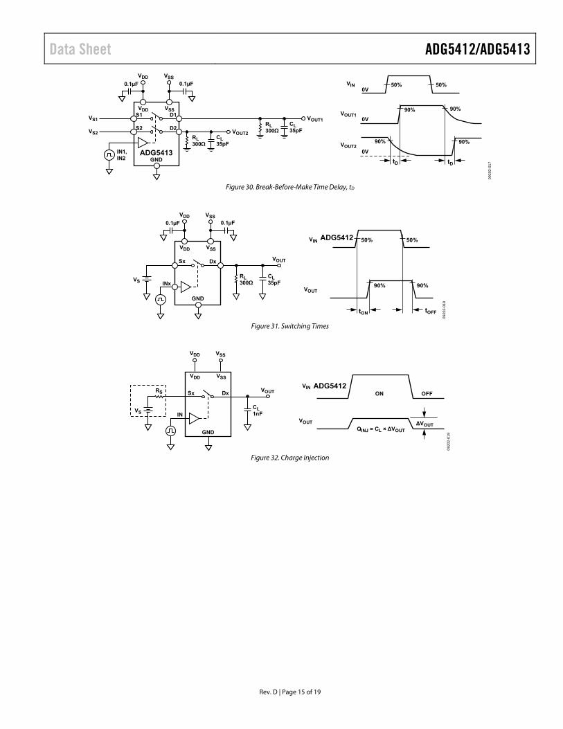
VS2
IN1,IN2
S2 D2
VS1S1 D1
GND
RL300Ω
CL35pF
VOUT2
VOUT1
VDD VSS
0.1µF
VDD
0.1µF
VSSVIN
VOUT1
VOUT2
ADG5413tD tD
50% 50%
90%90%
90%90%
0V
0V
0V
RL300Ω
CL35pF
092
02-0
17
Figure 30. Break-Before-Make Time Delay, tD
VS INx
Sx Dx
GND
RL300Ω
CL35pF
VOUT
VDD VSS
0.1µF
VDD
0.1µF
VSS
ADG5412VIN
VOUT
tON tOFF
50% 50%
90% 90%
092
02-0
18
Figure 31. Switching Times
IN
VOUTADG5412VIN
VOUT
OFF
∆VOUT
ON
QINJ = CL × ∆VOUT
Sx Dx
VDD VSS
VDD VSS
VS
RS
GND
CL1nF
092
02-0
19
Figure 32. Charge Injection

ADG5412/ADG5413 Data Sheet
Rev. D | Page 16 of 19
TERMINOLOGY IDD IDD represents the positive supply current.
ISS ISS represents the negative supply current.
VD, VS VD and VS represent the analog voltage on Terminal D and Terminal S, respectively.
RON RON represents the ohmic resistance between Terminal D and Terminal S.
∆RON ∆RON represents the difference between the RON of any two channels.
RFLAT (ON)
Flatness that is defined as the difference between the maximum and minimum value of on resistance measured over the specified analog signal range is represented by RFLAT (ON).
IS (Off) IS (Off) is the source leakage current with the switch off.
ID (Off) ID (Off) is the drain leakage current with the switch off.
ID (On), IS (On) ID (On) and IS (On) represent the channel leakage currents with the switch on.
VINL VINL is the maximum input voltage for Logic 0.
VINH VINH is the minimum input voltage for Logic 1.
IINL, IINH IINL and IINH represent the low and high input currents of the digital inputs.
CD (Off) CD (Off) represents the off switch drain capacitance, which is measured with reference to ground.
CS (Off) CS (Off) represents the off switch source capacitance, which is measured with reference to ground.
CD (On), CS (On) CD (On) and CS (On) represent on switch capacitances, which are measured with reference to ground.
CIN CIN is the digital input capacitance.
tON tON represents the delay between applying the digital control input and the output switching on.
tOFF tOFF represents the delay between applying the digital control input and the output switching off.
tD tD represents the off time measured between the 80% point of both switches when switching from one address state to another.
Off Isolation Off isolation is a measure of unwanted signal coupling through an off switch.
Charge Injection Charge injection is a measure of the glitch impulse transferred from the digital input to the analog output during switching.
Crosstalk Crosstalk is a measure of unwanted signal that is coupled through from one channel to another as a result of parasitic capacitance.
Bandwidth Bandwidth is the frequency at which the output is attenuated by 3 dB.
On Response On response is the frequency response of the on switch.
Insertion Loss Insertion loss is the loss due to the on resistance of the switch.
Total Harmonic Distortion + Noise (THD + N) The ratio of the harmonic amplitude plus noise of the signal to the fundamental is represented by THD + N.
AC Power Supply Rejection Ratio (ACPSRR) ACPSRR is the ratio of the amplitude of signal on the output to the amplitude of the modulation. This is a measure of the ability of the part to avoid coupling noise and spurious signals that appear on the supply voltage pin to the output of the switch. The dc voltage on the device is modulated by a sine wave of 0.62 V p-p.

Data Sheet ADG5412/ADG5413
Rev. D | Page 17 of 19
TRENCH ISOLATION In the ADG5412 and ADG5413, an insulating oxide layer (trench) is placed between the NMOS and the PMOS transistors of each CMOS switch. Parasitic junctions, which occur between the transistors in junction isolated switches, are eliminated, and the result is a completely latch-up proof switch.
In junction isolation, the N and P wells of the PMOS and NMOS transistors form a diode that is reverse-biased under normal operation. However, during overvoltage conditions, this diode can become forward-biased. A silicon controlled rectifier (SCR) type circuit is formed by the two transistors causing a significant amplification of the current that, in turn, leads to latch-up. With trench isolation, this diode is removed, and the result is a latch-up proof switch.
0920
2-0
22
NMOS PMOS
P-WELL N-WELL
BURIED OXIDE LAYER
HANDLE WAFER
TRENCH
Figure 33. Trench Isolation
ADG5412/ADG5413 Data Sheet
Rev. D | Page 18 of 19
APPLICATIONS INFORMATION The high voltage latch-up proof family of switches and multiplexers provide a robust solution for instrumentation, industrial, automo-tive, aerospace, and other harsh environments that are prone to latch-up, which is an undesirable high current state that can lead to device failure and persists until the power supply is turned off. The ADG5412/ADG5413 high voltage switches allow
single-supply operation from 9 V to 40 V and dual-supply operation from ±9 V to ±22 V. The ADG5412/ADG5413 (as well as other select devices within the same family) achieve an 8 kV human body model ESD rating, which provides a robust solution eliminating the need for separate protect circuitry designs in some applications.

Data Sheet ADG5412/ADG5413
Rev. D | Page 19 of 19
OUTLINE DIMENSIONS
16 9
81
PIN 1
SEATINGPLANE
8°0°
4.504.404.30
6.40BSC
5.105.004.90
0.65BSC
0.150.05
1.20MAX
0.200.09 0.75
0.600.45
0.300.19
COPLANARITY0.10
COMPLIANT TO JEDEC STANDARDS MO-153-AB Figure 34. 16-Lead Thin Shrink Small Outline Package [TSSOP]
(RU-16) Dimensions shown in millimeters
2.702.60 SQ2.50
COMPLIANT TO JEDEC STANDARDS MO-220-WGGC.
1
0.65BSC
BOTTOM VIEWTOP VIEW
16
589
1213
4
EXPOSEDPAD
PIN 1INDICATOR
4.104.00 SQ3.90
0.450.400.35
SEATINGPLANE
0.800.750.70 0.05 MAX
0.02 NOM
0.20 REF
0.20 MIN
COPLANARITY0.08
PIN 1INDICATOR
0.350.300.25
FOR PROPER CONNECTION OFTHE EXPOSED PAD, REFER TOTHE PIN CONFIGURATION ANDFUNCTION DESCRIPTIONSSECTION OF THIS DATA SHEET.
08-1
6-20
10-C
Figure 35. 16-Lead Lead Frame Chip Scale Package [LFCSP]
4 mm × 4 mm Body and 0.75 mm Package Height (CP-16-17)
Dimensions shown in millimeters
ORDERING GUIDE Model1
,2 Temperature Range Package Description Package Option
ADG5412BRUZ −40°C to +125°C 16-Lead Thin Shrink Small Outline Package [TSSOP] RU-16 ADG5412BRUZ-REEL7 −40°C to +125°C 16-Lead Thin Shrink Small Outline Package [TSSOP] RU-16 ADG5412BCPZ-REEL7 −40°C to +125°C 16-Lead Lead Frame Chip Scale Package [LFCSP] CP-16-17 ADG5413BRUZ −40°C to +125°C 16-Lead Thin Shrink Small Outline Package [TSSOP] RU-16 ADG5413BRUZ-REEL7 −40°C to +125°C 16-Lead Thin Shrink Small Outline Package [TSSOP] RU-16 ADG5413BCPZ-REEL7 −40°C to +125°C 16-Lead Lead Frame Chip Scale Package [LFCSP] CP-16-17 EVAL-16TSSOPEBZ Evaluation Board 1 Z = RoHS Compliant Part. 2 The EVAL-16TSSOPEBZ can be used to test the ADG5412 and the ADG5413.
©2010–2017 Analog Devices, Inc. All rights reserved. Trademarks and registered trademarks are the property of their respective owners. D09202-0-11/17(D)