Embed Size (px)
Citation preview
CO
www.advmat.de
MM
UNIC
Highly Efficient Polymer White-Light-Emitting DiodesBased on Lithium Salts Doped Electron TransportingLayer
ATIO
By Fei Huang, Ping-I. Shih, Ching-Fong Shu, Yun Chi, and Alex K.-Y. Jen*N
[*] Prof. A. K.-Y. Jen, Dr. F. HuangDepartment of Materials Science and EngineeringInstitute of Advanced Materials and TechnologyUniversity of WashingtonBox 352120, Seattle, WA 98195-2120 (USA)E-mail: [email protected]
Dr. P.-I. Shih, Prof. C.-F. ShuDepartment of Applied ChemistryNational Chiao Tung UniversityHsinchu, 300 (Taiwan ROC)
Prof. Y. ChiDepartment of Chemistry, National Tsing Hua UniversityHsin-Chu (Taiwan ROC)
DOI: 10.1002/adma.200802179
Adv. Mater. 2009, 21, 361–365 � 2009 WILEY-VCH Verlag Gm
Organic white-light-emitting diodes (OWLEDs) have attractedconsiderable attention due to their potential applications in full-color flat panel displays, back-lighting sources for liquid-crystaldisplays, and solid-state lighting.[1–3] To achieve high-efficiencyOWLEDs, efficient and balanced electron and hole injection andtransport from cathode and anode are essential. This results incommonly used multilayer device structures, including thetransparent conducting indium tin oxide (ITO) anode, hole-transport/injection layer (HTL), emissive layer (EML), electron-transport/injection layer (ETL), and metal cathode. For smallmolecule OWLEDs, this kind of multilayer structure can be easilyproduced by vacuum deposition with very thin emissive andtransport layers to maximize light output and minimize powerconsumption of the devices. As a result, vacuum depositedOWLEDs have exhibited higher efficiencies than standardincandescent light sources (13–20 lm W�1).[2–7] PolymerOWLEDs combining the advantages of simpler fabrication andlower production cost, especially for the large-area devices, areparticularly attractive, because they can be fabricated by simpletechniques like spin-coating or ink-jet printing.[8–20] However, it isvery difficult to realize well-controlled multilayer device struc-tures for polymer OWLEDs. Therefore, polymer OWLEDs oftenexhibit poorer performance than those obtained from smallmolecule OWLEDs. Only very few polymer OWLEDs reported sofar have efficiencies comparable to that of the incandescent lightbulbs.[14,19] Yang et al. have recently reported high-performancepolymer OWLEDs with a power efficiency (PE) of 16 lm W�1
using Cs2CO3 as the electron-injection/hole blocking layer in thedevices.[14] By using an alcohol-soluble conjugated polymer asETL, we have also shown high-efficiency polymer phosphorescentOWLEDs with a PE of 14.5 lm W�1.[19]
One of the most challenging problems for solution processedpolymer OWLEDs is that their transport and emissive layers need
to be thicker than those of the small molecule OWLEDs in orderto minimize pinhole formation on the films and to balance thehole and electron recombination in the devices. Because most ofthe organic semiconductors possess relatively low carrierconcentration and mobility,[21,22] thicker organic layers oftenresult in increased driving voltage for the devices, and causemorepower consumption. One way to overcome this limitation is touse dopedHTL/ETL to enhance device performance.[23] Althoughp-doped poly(3,4-ethylene-dioxythiophene): poly(styrene sulfonicacid) (PEDOT:PSS) has been widely used in PLEDs to improvehole injection and transport, the successful development of n-doped materials for efficient electron injection and transportremains very challenging, due to the difficulty of finding suitablehosts and dopants.
Until recently, several water/alcohol soluble conjugated poly-mers were demonstrated to be good ETLmaterials for OLEDs. Thepolar groups on their side chains can form interfacial dipolesbetween the EML and metal cathode to enhance electroninjection.[24–30] The unique solubility and excellent injection abilityof thesematerials offer the possibility to improve electron injectionand conductionbydoping themwithwater-soluble alkali or alkalineearth-metal salts,whichhavebeensuccessfullyusedasn-dopants inOLEDs.[31–33] Among these materials, the newly developed water/alcohol-soluble neutral conjugated polymers are ideal hosts for n-doping, because they do not involve the complexity of the counterions in conjugated polyelectrolytes.[19,30] In this Communication,we report highly efficient polymer OWLEDs derived from theLi2CO3-doped water/alcohol-soluble neutral conjugated polymerpoly[9,9-bis(2-(2-(2-diethanolamino ethoxy)ethoxy)ethyl) fluorene](PF-OH) ETL. It was found that the electron transporting ability ofPF-OH ETL can be dramatically improved upon doping withLi2CO3 salt. Consequently, very-high-efficiency polymer OWLEDswith a maximum forward viewing luminous efficiency (LE) of36.1 cd A�1 (61.4 cd A�1 for total viewing) and PE of 23.4 lm W�1
(39.8 lmW�1 for total viewing)were achieved, which is comparableto those reported from the state-of-the-art vacuum-deposited small-molecule OWLEDs.[2–7]
As shown in Scheme 1, the device configuration usedin this study is ITO/PEDOT:PSS(30nm)/FIrpic (7 wt%):Os-O(0.25 wt%):PVK:OXD-7(30 wt%) (70 nm)/ETL/Ba(4 nm)/Al(120 nm), where PEDOT:PSS is used as the hole-injecting/-transporting layer (HTL), sky-blue phosphorescent iridiumcomplex bis[(4,6-di-fluorophenyl)-pyridinato-N,C2] (picolinate)Ir(III) (FIrpic) and orange phosphorescent osmium complex(Os-O) are codoped into poly (N-vinylcarbazole) (PVK) host as theEML for white-light emission. 1,3-Bis[(4-tert-butylphenyl)-1,3,4-oxidiazolyl]phenylene (OXD-7) is incorporated to improveelectron transport of the EML. Doped PF-OH (doped with
bH & Co. KGaA, Weinheim 361
COM
MUNIC
ATIO
N
www.advmat.de
Scheme 1. Schematic of the device structure based on doped ETL andchemical structure of relevant materials.
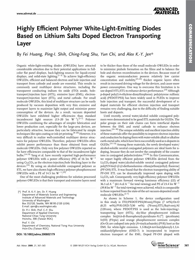
Figure 1. AFM images (3 mm�mm scale) of the PF-OH films spin-coatedon top of the emissive layer. a) PF-OH, b) PF-OH doped with 5 wt% Li2CO3,c) PF-OH doped with 15 wt% Li2CO3, d) PF-OH doped with 30 wt%Li2CO3.
362
5 wt%, 15 wt%, 30 wt% Li2CO3) or undoped PF-OH are used asthe ETL. The chemical structures of the relevant materials areshown in Scheme 1.
In our previous work, the optimal condition for processingneutral ETL materials in phosphorescent PLEDs was to usealcohol/water as cosolvent for spin-coating.[19,30] This facilitatesthe use of PF-OH as host for incorporating water-soluble alkalior alkaline earth-metal salts dopants, which have beensuccessfully used as n-dopants in OLEDs.[31–33] Atomic force
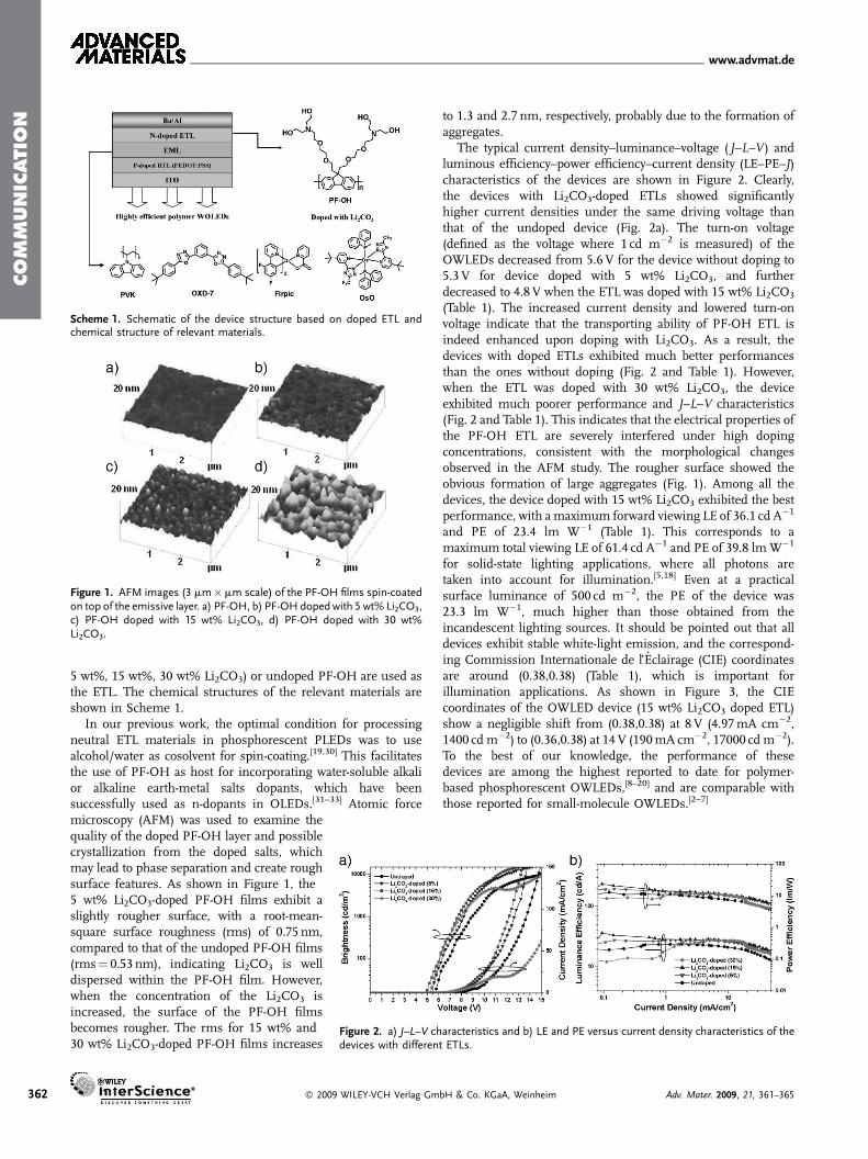
Figure 2. a) J–L–V characteristics and b) LE and PE versus current density characteristics of thedevices with different ETLs.
microscopy (AFM) was used to examine thequality of the doped PF-OH layer and possiblecrystallization from the doped salts, whichmay lead to phase separation and create roughsurface features. As shown in Figure 1, the5 wt% Li2CO3-doped PF-OH films exhibit aslightly rougher surface, with a root-mean-square surface roughness (rms) of 0.75 nm,compared to that of the undoped PF-OH films(rms¼ 0.53 nm), indicating Li2CO3 is welldispersed within the PF-OH film. However,when the concentration of the Li2CO3 isincreased, the surface of the PF-OH filmsbecomes rougher. The rms for 15 wt% and30 wt% Li2CO3-doped PF-OH films increases
� 2009 WILEY-VCH Verlag Gm
to 1.3 and 2.7 nm, respectively, probably due to the formation ofaggregates.
The typical current density–luminance–voltage ( J–L–V) andluminous efficiency–power efficiency–current density (LE–PE–J)characteristics of the devices are shown in Figure 2. Clearly,the devices with Li2CO3-doped ETLs showed significantlyhigher current densities under the same driving voltage thanthat of the undoped device (Fig. 2a). The turn-on voltage(defined as the voltage where 1 cd m�2 is measured) of theOWLEDs decreased from 5.6V for the device without doping to5.3 V for device doped with 5 wt% Li2CO3, and furtherdecreased to 4.8 V when the ETL was doped with 15 wt% Li2CO3
(Table 1). The increased current density and lowered turn-onvoltage indicate that the transporting ability of PF-OH ETL isindeed enhanced upon doping with Li2CO3. As a result, thedevices with doped ETLs exhibited much better performancesthan the ones without doping (Fig. 2 and Table 1). However,when the ETL was doped with 30 wt% Li2CO3, the deviceexhibited much poorer performance and J–L–V characteristics(Fig. 2 and Table 1). This indicates that the electrical properties ofthe PF-OH ETL are severely interfered under high dopingconcentrations, consistent with the morphological changesobserved in the AFM study. The rougher surface showed theobvious formation of large aggregates (Fig. 1). Among all thedevices, the device doped with 15 wt% Li2CO3 exhibited the bestperformance, with amaximum forward viewing LE of 36.1 cd A�1
and PE of 23.4 lm W�1 (Table 1). This corresponds to amaximum total viewing LE of 61.4 cd A�1 and PE of 39.8 lmW�1
for solid-state lighting applications, where all photons aretaken into account for illumination.[5,18] Even at a practicalsurface luminance of 500 cd m�2, the PE of the device was23.3 lm W�1, much higher than those obtained from theincandescent lighting sources. It should be pointed out that alldevices exhibit stable white-light emission, and the correspond-ing Commission Internationale de l’Eclairage (CIE) coordinatesare around (0.38,0.38) (Table 1), which is important forillumination applications. As shown in Figure 3, the CIEcoordinates of the OWLED device (15 wt% Li2CO3 doped ETL)show a negligible shift from (0.38,0.38) at 8 V (4.97mA cm�2,1400 cd m�2) to (0.36,0.38) at 14V (190mA cm�2, 17000 cd m�2).To the best of our knowledge, the performance of thesedevices are among the highest reported to date for polymer-based phosphorescent OWLEDs,[8–20] and are comparable withthose reported for small-molecule OWLEDs.[2–7]
bH & Co. KGaA, Weinheim Adv. Mater. 2009, 21, 361–365
COM
MUNIC
ATIO
N
www.advmat.de
Table 1. Device performance (forward-viewing) of OWLEDs using different ETL in the device configuration: ITO/PEDOT:PSS/FIrpic(7 wt%):Os-O(0.25wt%):PVK:OXD-7(30 wt%)/ETL/Ba/Al.
Device with different ETL Non-doped PF-OH Li2CO3-doped PF-OH Li2CO3-doped PF-OH Li2CO3-doped PF-OH
Dopant concentration 0 wt % 5wt % 15wt % 30wt %
Turn-on voltage (V) 5.6 5.3 4.8 5.2
E.Q.E. (%)[a] 9.2 10.5 12.6 6.9
L.E. (cd A�1)[a] 22.7 26.7 32.0 18.1
P.E. (lm W�1)[a] 11.7 15.1 18.5 9.5
Max brightness (cd m�2) 10720 (@ 16 V) 18200 (@ 17 V) 19580 (@ 16 V) 10800 (@ 16V)
Max E.Q.E. (%) 9.4 10.8 14.2 11.1
Max L.E. (cd A�1) 23.7 27.6 36.1 27.7
Max P.E. (lm W�1) 12.9 16.6 23.4 12.2
Voc 2.0 2.0 2.0 1.9
CIE, x and y[b] 0.39 and 0.39 0.38 and 0.38 0.38 and 0.38 0.37 and 0.38
[a] Recorded at 100 cd m�2. [b] At 8 V.
Figure 4. Photovoltaic characteristics of devices with different ETLs.Figure 3. Normalized EL spectra of OWLED with 15 wt% Li2CO3 dopedETL at various driving voltages.
The significantly improved device performance originatesfrom the improved current density of PF-OH ETL upon doping.There are two possible mechanisms that may contribute to thiseffect: either the improved charge transport[23] or the improvedelectron-injection ability of the PF-OH ETL from the metal
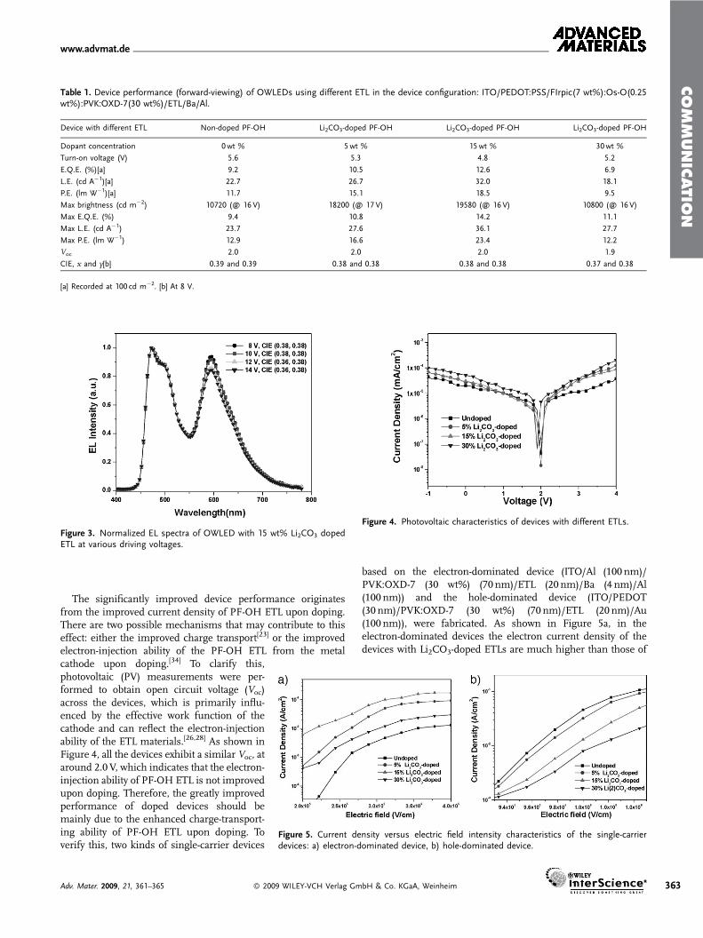
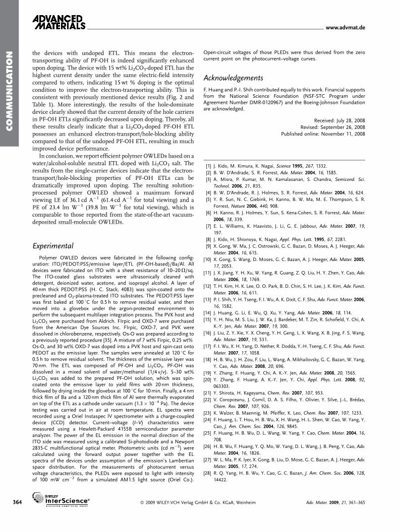
Figure 5. Current density versus electric field intensity characteristics of the single-carrierdevices: a) electron-dominated device, b) hole-dominated device.
cathode upon doping.[34] To clarify this,photovoltaic (PV) measurements were per-formed to obtain open circuit voltage (Voc)across the devices, which is primarily influ-enced by the effective work function of thecathode and can reflect the electron-injectionability of the ETL materials.[26,28] As shown inFigure 4, all the devices exhibit a similar Voc, ataround 2.0 V, which indicates that the electron-injection ability of PF-OH ETL is not improvedupon doping. Therefore, the greatly improvedperformance of doped devices should bemainly due to the enhanced charge-transport-ing ability of PF-OH ETL upon doping. Toverify this, two kinds of single-carrier devices
Adv. Mater. 2009, 21, 361–365 � 2009 WILEY-VCH Verlag Gm
based on the electron-dominated device (ITO/Al (100 nm)/PVK:OXD-7 (30 wt%) (70 nm)/ETL (20 nm)/Ba (4 nm)/Al(100 nm)) and the hole-dominated device (ITO/PEDOT(30 nm)/PVK:OXD-7 (30 wt%) (70 nm)/ETL (20 nm)/Au(100 nm)), were fabricated. As shown in Figure 5a, in theelectron-dominated devices the electron current density of thedevices with Li2CO3-doped ETLs are much higher than those of
bH & Co. KGaA, Weinheim 363
COM
MUNIC
ATIO
N
www.advmat.de
364
the devices with undoped ETL. This means the electron-transporting ability of PF-OH is indeed significantly enhancedupon doping. The device with 15 wt% Li2CO3-doped ETL has thehighest current density under the same electric-field intensitycompared to others, indicating 15wt % doping is the optimalcondition to improve the electron-transporting ability. This isconsistent with previously mentioned device results (Fig. 2 andTable 1). More interestingly, the results of the hole-dominatedevice clearly showed that the current density of the hole carriersin PF-OH ETLs significantly decreased upon doping. Thereby, allthese results clearly indicate that a Li2CO3-doped PF-OH ETLpossesses an enhanced electron-transport/hole-blocking abilitycompared to that of the undoped PF-OH ETL, resulting in muchimproved device performance.
In conclusion, we report efficient polymer OWLEDs based on awater/alcohol-soluble neutral ETL doped with Li2CO3 salt. Theresults from the single-carrier devices indicate that the electron-transport/hole-blocking properties of PF-OH ETLs can bedramatically improved upon doping. The resulting solution-processed polymer OWLED showed a maximum forwardviewing LE of 36.1 cd A�1 (61.4 cd A�1 for total viewing) and aPE of 23.4 lm W�1 (39.8 lm W�1 for total viewing), which iscomparable to those reported from the state-of-the-art vacuum-deposited small-molecule OWLEDs.
Experimental
Polymer OWLED devices were fabricated in the following config-uration: ITO/PEDOT:PSS/emissive layer/ETL (PF-OH-based)/Ba/Al. Alldevices were fabricated on ITO with a sheet resistance of 10–20V/sq.The ITO-coated glass substrates were ultrasonically cleaned withdetergent, deionized water, acetone, and isopropyl alcohol. A layer of40 nm thick PEDOT:PSS (H. C. Stack, 4083) was spin-coated onto theprecleaned and O2-plasma-treated ITO substrates. The PEDOT:PSS layerwas first baked at 100 8C for 0.5 h to remove residual water, and thenmoved into a glovebox under the argon-protected environment toperform the subsequent multilayer integration process. The PVK host andLi2CO3 were purchased from Aldrich. FIrpic and OXD-7 were purchasedfrom the American Dye Sources Inc. FIrpic, OXD-7, and PVK weredissolved in chlorobenzene, respectively. Os-O was prepared according toa previously reported procedure [35]. A mixture of 7 wt% Firpic, 0.25 wt%Os-O, and 30 wt% OXD-7 was doped into a PVK host and spin-cast ontoPEDOT as the emissive layer. The samples were annealed at 120 8C for0.5 h to remove residual solvent. The thickness of the emissive layer was70 nm. The ETL was composed of PF-OH and Li2CO3. PF-OH wasdissolved in a mixed solvent of water/methanol (1/4 v/v). 5–30 wt%Li2CO3 was added to the prepared PF-OH solution, which was spin-coated onto the emissive layer to yield films with 20 nm thickness,followed by drying inside the glovebox at 100 8C for 10min. Finally, a 4 nmthick film of Ba and a 120 nm thick film of Al were thermally evaporatedon top of the ETL as a cathode under vacuum (1.3� 10�4 Pa). The devicetesting was carried out in air at room temperature. EL spectra wererecorded using a Oriel Instaspec IV spectrometer with a charge-coupleddevice (CCD) detector. Current–voltage (I–V) characteristics weremeasured using a Hewlett-Packard 4155B semiconductor parameteranalyzer. The power of the EL emission in the normal direction of theITO side was measured using a calibrated Si-photodiode and a Newport2835-C multifunctional optical meter. Photometric units (cd m�2) werecalculated using the forward output power together with the ELspectra of the devices under assumption of the emission’s Lambertianspace distribution. For the measurements of photocurrent versusvoltage characteristics, the PLEDs were exposed to light with intensityof 100 mW cm�2 from a simulated AM1.5 light source (Oriel Co.).
� 2009 WILEY-VCH Verlag Gm
Open-circuit voltages of those PLEDs were thus derived from the zerocurrent point on the photocurrent–voltage curves.
Acknowledgements
F. Huang and P.-I. Shih contributed equally to this work. Financial supportsfrom the National Science Foundation (NSF-STC Program underAgreement Number DMR-0120967) and the Boeing-Johnson Foundationare acknowledged.
Received: July 28, 2008
Revised: September 26, 2008
Published online: November 11, 2008
[1] J. Kido, M. Kimura, K. Nagai, Science 1995, 267, 1332.
[2] B. W. D’Andrade, S. R. Forrest, Adv. Mater. 2004, 16, 1585.
[3] A. Misra, P. Kumar, M. N. Kamalasanan, S. Chandra, Semicond. Sci.
Technol. 2006, 21, R35.
[4] B. W. D’Andrade, R. J. Holmes, S. R. Forrest, Adv. Mater. 2004, 16, 624.
[5] Y. R. Sun, N. C. Giebink, H. Kanno, B. W. Ma, M. E. Thompson, S. R.
Forrest, Nature 2006, 440, 908.
[6] H. Kanno, R. J. Holmes, Y. Sun, S. Kena-Cohen, S. R. Forrest, Adv. Mater.
2006, 18, 339.
[7] E. L. Williams, K. Haavisto, J. Li, G. E. Jabbour, Adv. Mater. 2007, 19,
197.
[8] J. Kido, H. Shionoya, K. Nagai, Appl. Phys. Lett. 1995, 67, 2281.
[9] X. Gong, W. Ma, J. C. Ostrowski, G. C. Bazan, D. Moses, A. J. Heeger, Adv.
Mater. 2004, 16, 615.
[10] X. Gong, S. Wang, D. Moses, G. C. Bazan, A. J. Heeger, Adv. Mater. 2005,
17, 2053.
[11] J. X. Jiang, Y. H. Xu, W. Yang, R. Guang, Z. Q. Liu, H. Y. Zhen, Y. Cao, Adv.
Mater. 2006, 18, 1769.
[12] T. H. Kim, H. K. Lee, O. O. Park, B. D. Chin, S. H. Lee, J. K. Kim, Adv. Funct.
Mater. 2006, 16, 611.
[13] P. I. Shih, Y. H. Tseng, F. I. Wu, A. K. Dixit, C. F. Shu, Adv. Funct. Mater. 2006,
16, 1582.
[14] J. Huang, G. Li, E. Wu, Q. Xu, Y. Yang, Adv. Mater. 2006, 18, 114.
[15] Y. H. Niu, M. S. Liu, J. W. Ka, J. Bardeker, M. T. Zin, R. Schofield, Y. Chi, A.
K.-Y. Jen, Adv. Mater. 2007, 19, 300.
[16] J. Liu, Z. Y. Xie, Y. X. Cheng, Y. H. Geng, L. X. Wang, X. B. Jing, F. S. Wang,
Adv. Mater. 2007, 19, 531.
[17] F. I. Wu, X. H. Yang, D. Nether, R. Dodda, Y.-H. Tseng, C. F. Shu, Adv. Funct.
Mater. 2007, 17, 1058.
[18] H. B. Wu, J. H. Zou, F. Liu, L. Wang, A. Mikhailovsky, G. C. Bazan, W. Yang,
Y. Cao, Adv. Mater. 2008, 20, 696.
[19] Y. Zhang, F. Huang, Y. Chi, A. K.-Y. Jen, Adv. Mater. 2008, 20, 1565.
[20] Y. Zhang, F. Huang, A. K.-Y. Jen, Y. Chi, Appl. Phys. Lett. 2008, 92,
063303.
[21] Y. Shirota, H. Kageyama, Chem. Rev. 2007, 107, 953.
[22] V. Coropceanu, J. Comil, D. A. S. Filho, Y. Olivier, Y. Silve, J.-L. Bredas,
Chem. Rev. 2007, 107, 926.
[23] K. Walzer, B. Maennig, M. Pfeiffer, K. Leo, Chem. Rev. 2007, 107, 1233.
[24] F. Huang, L. T. Hou, H. B. Wu, X. H. Wang, H. L. Shen, W. Cao, W. Yang, Y.
Cao, J. Am. Chem. Soc. 2004, 126, 9845.
[25] F. Huang, H. B. Wu, D. L. Wang, W. Yang, Y. Cao, Chem. Mater. 2004, 16,
708.
[26] H. B. Wu, F. Huang, Y. Q. Mo, W. Yang, D. L. Wang, J. B. Peng, Y. Cao, Adv.
Mater. 2004, 16, 1826.
[27] W. L. Ma, P. K. Iyer, X. Gong, B. Liu, D. Mose, G. C. Bazan, A. J. Heeger, Adv.
Mater. 2005, 17, 274.
[28] R. Q. Yang, H. B. Wu, Y. Cao, G. C. Bazan, J. Am. Chem. Soc. 2006, 128,
14422.
bH & Co. KGaA, Weinheim Adv. Mater. 2009, 21, 361–365

COM
MUNI
www.advmat.de
[29] S. H. Oh, S. I. Na, Y. C. Nah, D. Vak, S. S. Kim, S. D. Y. Kim, Org. Electron.
2007, 8, 773.
[30] F. Huang, Y. H. Niu, Y. Zhang, J. W. Ka, M. S. Liu, A. K.-Y. Jen, Adv. Mater.
2007, 19, 2010.
[31] T.-W. Lee, T. Noh, B.-K. Choi, M.-S. Kim, D. W. Shin, J. Kido, Appl. Phys. Lett.
2008, 92, 043301.
Adv. Mater. 2009, 21, 361–365 � 2009 WILEY-VCH Verlag Gm
[32] K. R. Choudhury, J.-h. Yoon, F. So, Adv. Mater. 2008, 20, 1456.
[33] C. C. Hsiao, A. E. Hsiao, S. A. Chen, Adv. Mater. 2008, 20, 1982.
[34] L. S. Hung, C. W. Tang, M. G. Mason, Appl. Phys. Lett. 1997, 70,
152.
[35] Y.-L. Tung, Ph. D. Thesis, National Tsing Hua University, Hsinchu, Taiwan
2005.
C
ATI ON
bH & Co. KGaA, Weinheim 365