Embed Size (px)
Citation preview

Highly Efficient Single-Phase Full-wave FAN Motor Driver Overview The HM2602 is a highly efficient Single-Phase Brushless DC FAN motor driver with direct PWM speed control. Many safety features were incorporated to ensure the reliability of motor operation. The HM2602 is designed with minimal external components to improve reliability. Package
HTSSOP14 TSSOP20
Application Variable speed BLDC fan for CPU/VGA cooler, power supplier, game console, etc.
Feature Speed Control with direct PWM input Soft-Start circuit FG output signal Built-in Hall bias circuit Minimum speed setting Soft switch for quiet drive Advanced CMOS process and low Rds Built-in triangular wave generator, No
capacitor need Built-in lock protection and automatic recovery
circuit, No capacitor need Built-in thermal shutdown protection(TSD) Built-in over current protection(OCP) Built-in under voltage lock out (UVLO)
Ordering information Name Package Model Order
HM2602H HTSSOP14 HM2602H-T(Tube) HM2602H-R(Reel)
HM2602T TSSOP20 HM2602T-T(Tube) HM2602T-R(Reel)
Block Diagram
TSD
Con
trol
En
gine
SAW Tooth Generator
Hall
LDO
PWM
HB
H_INN
H_INP
VREG6
VCC
FG
VSS
1.25V
Pre Driver
F-GND
MOTU
MOTV
M
SMIN
LockProtection
ocp
HM2602
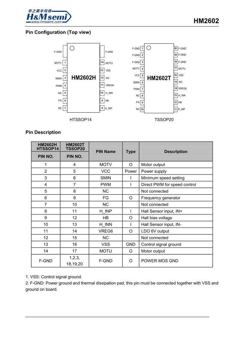
Pin Configuration (Top view)
FA2200
F-GND
MOTV
VCC
SMIN
PWM
NC
FG
NC
MOTU
F-GND
VSS
NC
VREG6
H_INN
HB
H_INP
1
2
3
4
5
6
7
9
8
10
11
12
13
14
HM2602HFA2200
F-GND
MOTV
VCC
SMIN
PWM
NC
FG
NC
MOTU
VSS
NC
VREG6
H_INN
HB
H_INP
1
2
3
4
5
6
7
13
14
15
16
17
HM2602T
8
9
F-GND
F-GND
20
10 11
12
18
19
F-GND
F-GND
F-GND
HTSSOP14 TSSOP20 Pin Description
HM2602H HM2602T PIN Name Type Description
PIN NO. PIN NO.
1 4 MOTV O Motor output 2 5 VCC Power Power supply 3 6 SMIN I Minimum speed setting 4 7 PWM I Direct PWM for speed control 5 8 NC Not connected 6 9 FG O Frequency generator 7 10 NC Not connected 8 11 H_INP I Hall Sensor input, IN+ 9 12 HB O Hall bias voltage 10 13 H_INN I Hall Sensor input, IN- 11 14 VREG6 O LDO 6V output 12 15 NC Not connected 13 16 VSS GND Control signal ground 14 17 MOTU O Motor output
F-GND 1,2,3,
18,19,20 F-GND O POWER MOS GND
1. VSS: Control signal ground. 2. F-GND: Power ground and thermal dissipation pad, this pin must be connected together with VSS and ground on board.
HTSSOP14 TSSOP20
HM2602
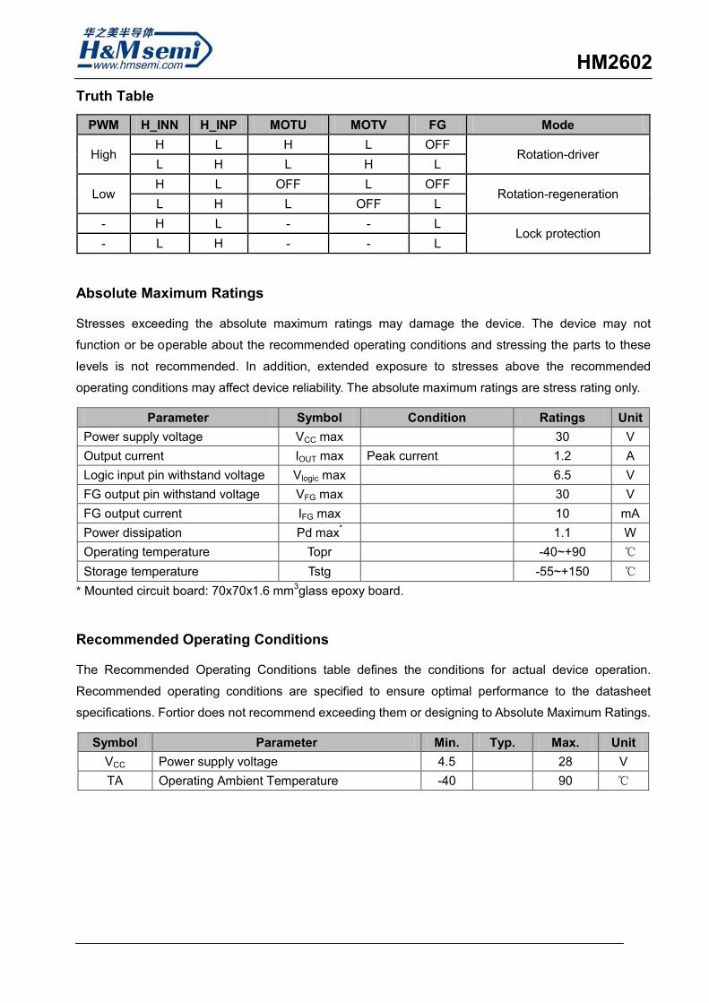
Truth Table
PWM H_INN H_INP MOTU MOTV FG Mode
High H L H L OFF
Rotation-driver L H L H L
Low H L OFF L OFF
Rotation-regeneration L H L OFF L
- H L - - L Lock protection
- L H - - L
Absolute Maximum Ratings
Stresses exceeding the absolute maximum ratings may damage the device. The device may not
function or be operable about the recommended operating conditions and stressing the parts to these
levels is not recommended. In addition, extended exposure to stresses above the recommended
operating conditions may affect device reliability. The absolute maximum ratings are stress rating only.
Parameter Symbol Condition Ratings Unit Power supply voltage VCC max 30 V Output current IOUT max Peak current 1.2 A Logic input pin withstand voltage Vlogic max 6.5 V FG output pin withstand voltage VFG max 30 V FG output current IFG max 10 mA Power dissipation Pd max* 1.1 W Operating temperature Topr -40~+90 ℃ Storage temperature Tstg -55~+150 ℃
* Mounted circuit board: 70x70x1.6 mm3glass epoxy board.
Recommended Operating Conditions
The Recommended Operating Conditions table defines the conditions for actual device operation.
Recommended operating conditions are specified to ensure optimal performance to the datasheet
specifications. Fortior does not recommend exceeding them or designing to Absolute Maximum Ratings.
Symbol Parameter Min. Typ. Max. Unit VCC Power supply voltage 4.5 28 V TA Operating Ambient Temperature -40 90 ℃
HM2602
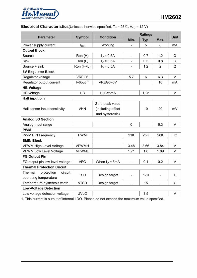
Electrical Characteristics(Unless otherwise specified, Ta = 25℃, VCC = 12 V)
Parameter Symbol Condition Ratings
Unit Min. Typ. Max.
Power supply current ICC Working - 5 8 mA Output Block Source Ron (H) IO = 0.5A - 0.7 1.2 Ω Sink Ron (L) IO = 0.5A - 0.5 0.8 Ω Source + sink Ron (H+L) IO = 0.5A - 1.2 2 Ω 6V Regulator Block Regulator voltage VREG6 5.7 6 6.3 V Regulator output current Iv6out(1) VREG6=6V 10 mA HB Voltage HB voltage HB I HB=5mA
1.25
V
Hall input pin
Hall sensor input sensitivity VHN Zero peak value (including offset and hysteresis)
10 20 mV
Analog I/O Section Analog Input range 0 6.3 V PWM PWM PIN Frequency PWM 21K 25K 28K Hz SMIN Block
VPWM High Level Voltage VPWMH 3.48 3.66 3.84 V VPWM Low Level Voltage VPWML 1.71 1.8 1.89 V FG Output Pin FG output pin low-level voltage VFG When IO = 5mA - 0.1 0.2 V Thermal Protection Circuit Thermal protection circuit operating temperature
TSD Design target - 170 - ℃
Temperature hysteresis width ΔTSD Design target - 15 - ℃ Low-Voltage Detection Low voltage detection voltage UVLO 3.5 V
1. This current is output of internal LDO. Please do not exceed the maximum value specified.
HM2602
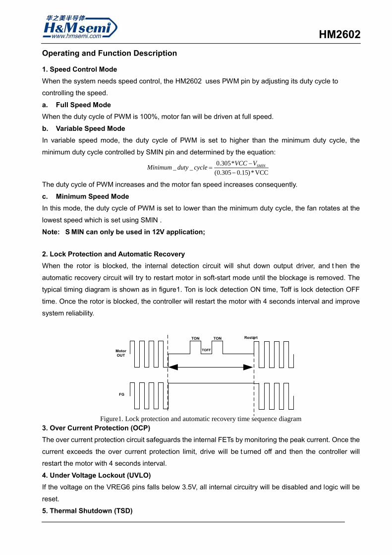
Figure1. Lock protection and automatic recovery time sequence diagram
Operating and Function Description
1. Speed Control Mode When the system needs speed control, the HM2602 uses PWM pin by adjusting its duty cycle to
controlling the speed.
a. Full Speed Mode When the duty cycle of PWM is 100%, motor fan will be driven at full speed.
b. Variable Speed Mode In variable speed mode, the duty cycle of PWM is set to higher than the minimum duty cycle, the
minimum duty cycle controlled by SMIN pin and determined by the equation: 0.305*_ _
(0.305 0.15)* VCCSMINVCC VMinimum duty cycle −
=−
The duty cycle of PWM increases and the motor fan speed increases consequently.
c. Minimum Speed Mode In this mode, the duty cycle of PWM is set to lower than the minimum duty cycle, the fan rotates at the
lowest speed which is set using SMIN .
Note: S MIN can only be used in 12V application;
2. Lock Protection and Automatic Recovery When the rotor is blocked, the internal detection circuit will shut down output driver, and t hen the
automatic recovery circuit will try to restart motor in soft-start mode until the blockage is removed. The
typical timing diagram is shown as in figure1. Ton is lock detection ON time, Toff is lock detection OFF
time. Once the rotor is blocked, the controller will restart the motor with 4 seconds interval and improve
system reliability.
TOFF
TON TON
FG
Restart
Motor OUT
3. Over Current Protection (OCP) The over current protection circuit safeguards the internal FETs by monitoring the peak current. Once the
current exceeds the over current protection limit, drive will be t urned off and then the controller will
restart the motor with 4 seconds interval.
4. Under Voltage Lockout (UVLO) If the voltage on the VREG6 pins falls below 3.5V, all internal circuitry will be disabled and logic will be
reset.
5. Thermal Shutdown (TSD)
HM2602
When the junction temperature of the device reaches the thermal shutdown limit(2) (the thermal
shutdown value is shown in Electrical Characteristics table), PWM drive output will be turned off. When
the junction temperature cools to the required level, the PWM initiates normal start-up cycle. Thermal
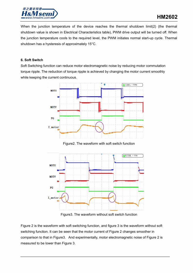
shutdown has a hysteresis of approximately 15°C. 6. Soft Switch Soft Switching function can reduce motor electromagnetic noise by reducing motor commutation
torque ripple. The reduction of torque ripple is achieved by changing the motor current smoothly
while keeping the current continuous.
Figure2. The waveform with soft switch function
Figure3. The waveform without soft switch function
Figure 2 is the waveform with soft switching function, and figure 3 is the waveform without soft
switching function. It can be seen that the motor current of Figure 2 changes smoother in
comparison to that in Figure3. And experimentally, motor electromagnetic noise of Figure 2 is
measured to be lower than Figure 3.
HM2602

12V Application Circuit
F-GND
NC
MOTV
NC
PWM
SMIN
FG
F-GND
H_INN
NC
VCC
H_INP
HB
VREG6
NC
VSS
MOTUVm
VDD6
Hall
HM2602
M
FG
VCC C1
Vm
Figure4. 12V application circuit of HM2602
24V Application Circuit
F-GND
NC
MOTV
NC
PWM
SMIN
FG
F-GND
H_INN
NC
VCC
H_INP
HB
VREG6
NC
VSS
MOTUVCC
Hall
M
FG
VIN C1
VCC
VCC
VDD6
1.0MΩ
Figure4. 24V application circuit of HM2602
Regenerative current absorption capacitor; Prevent
reverse-connectio
Direct PWM speed control
Protection resistor
Bypass capacitor;
TVS, surge voltage protector
Minimum Speed setting Regenerative current absorption capacitor;
Prevent reverse-connection
Direct PWM speed control
Protection resistor
Bypass capacitor; close to VREG6
HM2602

Application notes: 1. Power and ground lines F-GND and VSS should be connected together on board.
2. Power supply bypass capacitor & TVS zener diodes The capacitor C1on VCC provides power supply stabilization for both PWM drive and kickback
absorption. When a diode is used to prevent destruction of controller IC from reverse connection, please
make sure to add capacitor C1 for routing of regenerative current, In order to protect surge voltage
damage, please insert a TVS zener diode between GND and VCC.
3. Hall input The Hall sensor input circuit consists of a comparator with hysteresis of 20mV. Hall sensor input level
with at least three times of this hysteresis, i.e. at least 60mVp-p is recommended.
4. FG output This is an open collector output, the pin must be left open if unused. FG output is used to reflect rotation
count, which corresponds to the phase switching. When lock protection , it will be zero all the time.
5. HB pin This pin provides constant-voltage output of 1.25V for hall effect sensor biasing.
6. SMIN pin This pin is used to set minimum speed by adjusting external resistors.
SMIM can only be used in 12V application. If 24V application, please connect 1M ohm resistor to VCC.
7. Motor capacitor Insert a capacitor between the MOTU and MOTV pin if the noise is a problem.
8. Motor terminal schottky diode Please insert schottky diode between the motor terminal and VCC for bigger current.
9. Motor terminal zener diode Please insert zener diode between the motor terminal and VSS for routing of regenerative current
HM2602

Package Information HTSSOP14
HM2602

TSSOP-20
MIN NOM MAX
A 一 一 1.20
A1 0.05 一 0.15
A2 0.80 1.00 1.05
b 0.19 一 0.30
b1 0.19 0.22 0.25
c 0.09 一 0.20
c1 0.09 一 0.16
D 6.40 6.50 6.60
E 6.20 6.40 6.60
E1 4.30 4.40 4.50
e 0.65BSC
L 0.45 0.60 0.75
L1 1.00BSC
HM2602