Embed Size (px)
Citation preview

Journal of Electrical Engineering & Technology Vol. 7, No. 4, pp. 582~588, 2012 http://dx.doi.org/10.5370/JEET.2012.7.4.582
582
Highly Miniaturized and Performed UWB Bandpass Filter Embedded into PCB with SrTiO3 Composite Layer
Seong Jong Cheon*, Jun Hwan Park** and Jae Yeong Park†
Abstract – In this paper, a highly miniaturized and performed UWB bandpass filter has been newly designed and implemented by embedding all the passive elements into a multi-layered PCB substrate with high dielectric SrTiO3 composite film for 3.1 - 4.75 GHz compact UWB system applications. The high dielectric composite film was utilized to increase the capacitance densities and quality factors of capacitors embedded into the PCB. In order to reduce the size of the filter and avoid parasitic EM coupling between the embedded filter circuit elements, it was designed by using a 3rd order Chebyshev circuit topology and a capacitive coupled transformation technology. Independent transmission zeros were also applied for improving the attenuation of the filter at the desired stopbands. The measured insertion and return losses in the passband were better than 1.68 and 12 dB, with a minimum value of 0.78 dB. The transmission zeros of the measured response were occurred at 2.2 and 5.15 GHz resulting in excellent suppressions of 31 and 20 dB at WLAN bands of 2.4 and 5.15 GHz, respectively. The size of the fabricated bandpass filter was 2.9 x 2.8 x 0.55 (H) mm3.
Keywords: Bandpass filters, Embedded passive devices (EPDs), Independent transmission zeros, J-inverter, Multi-layered PCB substrate, High dielectric composite, Ultra wideband (UWB)
1. Introduction
Since the UWB technology is very attractive and promising for high-speed wireless data delivery, much research has been performed to develop highly functional and miniaturized UWB bandpass filters. In particular, the filter with a passband ranged from 3.1 GHz to 4.75 GHz are being actively researched, since it can avoid wireless local area network (WLAN) bands of 2.4 GHz (IEEE 802.11 b/g) and 5.15 GHz (IEEE 802.11 a). There are several research issues for its commercialization such as high rejection performance, small size/volume, and low cost fabrication. In order to obtain the good rejection performances of the filter at the WLAN bands, the distributed-elements such as microstrip lines, strip lines, and coplanar waveguides, have been applied [1, 2]. Since the distributed type filters had some limitations for reducing their sizes/volumes, the lumped type filters have been investigated by embedding passive elements into multi-layered substrates such as low-temperature co-fired ceramic (LTCC) and printed circuit board (PCB) [3-7]. Although the LTCC fabrication technology is effective for miniaturizing the filters, it still suffers from some temperature-related failures for large area manufacturing [1-5]. Recently, fully embedded high quality factor (Q)
inductors and capacitors have been investigated onto the PCB [8, 9]. For fabricating the high density capacitors, barium titanate (BaTiO3) and barium strontium titanate (BaSrTiO3) composite materials were utilized [10].
In order to highly improve the rejection characteristics at the desired stop bands, adding external notch resonators or finite transmission zeros were investigated. Since the external notch resonators were formed using radial or tee stubs, ring, and unit or stepped impedance resonators, the size of filter was relatively large [1, 2]. Since the finite transmission zeros could be easily formed by adding an inductor or a capacitor, they have recently been used in the lumped-element filter circuits to form a feedback path by adding inductive or capacitive coupling components between the input and output ports [3, 4]. However, these inductive or capacitive coupling methods needed relatively large component values and generated the unwanted electromagnetic (EM) coupling between the filter circuit elements. Another approach was to form a shunt resonator by adding a capacitor or an inductor in series with parallel resonators [5, 6]. However, it was difficult to design and optimize the filter circuit, since these finite transmission zeros were dependent each other.
In this paper, highly miniaturized and performed UWB bandpass filter was newly developed by embedding all the filter circuit elements into a low cost PCB substrate. For miniaturizing the filter circuit, PCB embedded capacitors with high Q and density of capacitance were fabricated by using high dielectric composite film, which was comprised of epoxy resin and strontium titanate (SrTiO3) powders. In order to avoid the parasitic EM coupling among the filter
† Corresponding Author: Dept. of Electronic Engineering, Kwangwoon University, Seoul, Korea. ([email protected])
* Dept. of Electronic Engineering, Kwangwoon University, Seoul, Korea. ([email protected])
** Dept. of Research & Division, Amkor technologies, Ltd., Seoul, Korea. ([email protected])
Received: May 17, 2011; Accepted: January 5, 2012

Seong Jong Cheon, Jun Hwan Park and Jae Yeong Park
583
circuit elements, a modified 3rd order Chebyshev circuit topology and the capacitive coupled type characteristic admittance of the inverter (J-inverter) transformation technology were applied, as shown in Fig. 1(a). In addition, to obtain maximum rejection characteristic in the desired stopbands, three independent transmission zeros were formed by connecting in series one capacitor and two inductors with the shunt LC resonators individually. These independent transmission zeros were very effective to design and optimize the filter circuit.
2. Design and Simulation The proposed filter was first designed by using T
prototype 3rd order Chebyshev filter circuit topology with 0.5 dB ripple for obtaining a large bandwidth, as shown in
Fig. 1(a) [11]. Since the T prototype filter was generally designed with several inductors with relatively large inductance values, its performance could be degraded due to the parasitic EM coupling between the inductors, when they were embedded with 3D transformed structure into a multi-layered PCB substrate [12]. In addition, since the quality factor and self resonant frequency of the large inductor decreased as operating frequency increased, the filter performance was also degraded.
To solve these problems, the J-inverter transformation technology was adopted to transfer the serial resonators into shunt ones and to improve the attenuation performance of the filter at the lower frequency band. Fig. 1(b) shows the J-inverter transformed 3rd order Chebyshev filter circuit, which is comprised of shunt LC resonators and admittance J-inverters. The inductance Li, capacitance Ci (i=1,2, …, n), and characteristic admittance Ji,i+1 (i=0,1, …, n) are given by the following equations
( )2
1 , 1 to , 1/ rad / seci Co i
L i nCω
= = Ω = (1)
0 0 1 0 101 , 1
0 1 1
1 0, 1
1
, ,i ii i
c c i i
n nn n
c n n
G W C W C CJ J
g g g g
G W CJ
g g
ω ω
ω
++
+
++
+
= =Ω Ω
=Ω
(2)
where the inductance Li (or capacitance Ci) and input and output impedances G0, Gn,n+1 may take arbitrary values, ωo is the central angular frequency of the bandpass filter, W is the fractional bandwidth, and gi (i=0,1,…, n+1) is the lowpass normalized parameters.
Since the J-inverter transformed filter circuit was designed to have relatively small inductance and large capacitance values compared with the T-type Chebyshev filter circuits shown in Fig. 1(a), it allowed much lower parasitic EM coupling than the T-type filter. Moreover, the J-inverter transformed filter provides more enhanced rejection characteristic at WLAN band of 2.4 GHz than the conventional T-type one.
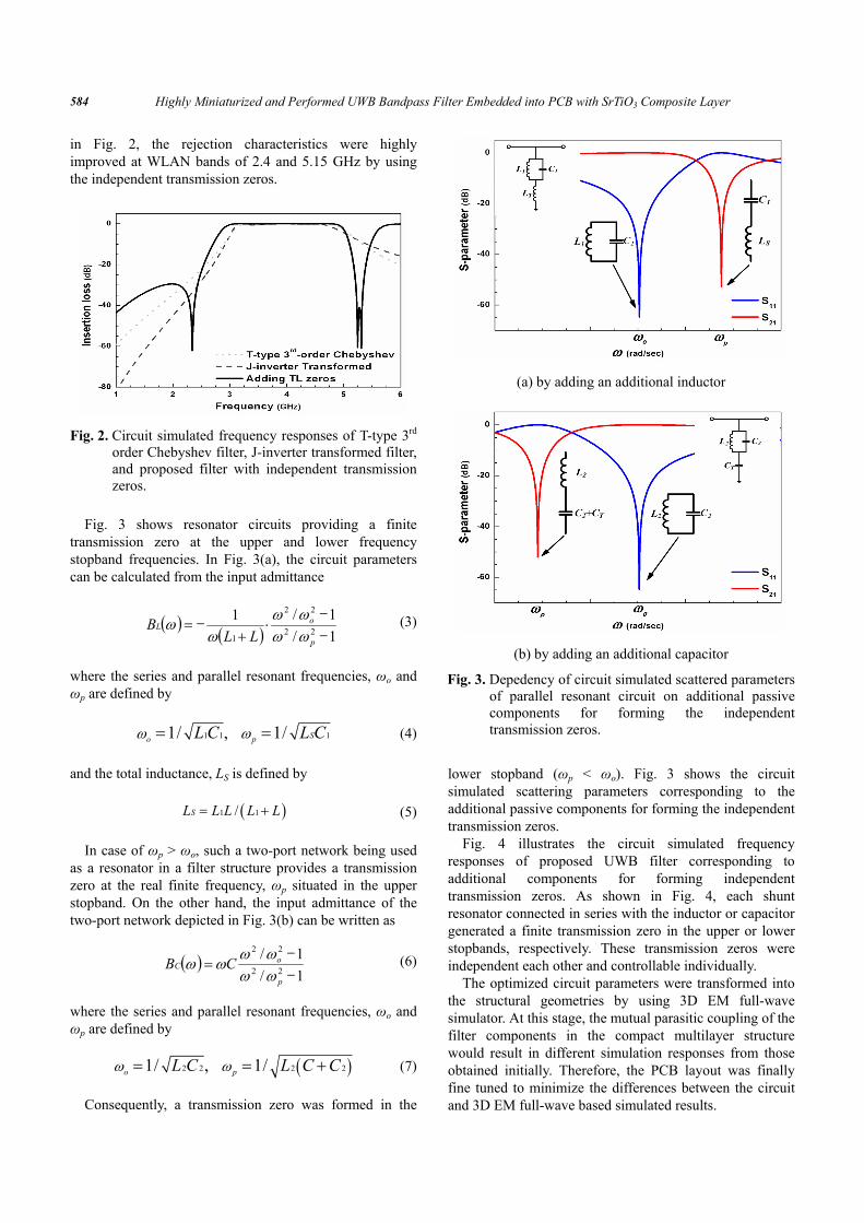
In addition, in order to improve the rejection characteristic in the desired stopband, finite transmission zero technology was applied by connecting a capacitor or an inductor with the shunt LC resonator [13]. The transmission zero appears at finite frequency due to a reactance connected in series with the shunt LC resonator. Fig. 1(c) shows the proposed UWB filter circuit with independent transmission zeros. In order to control the rejection characteristics independently at lower and higher frequency bands, a capacitor and two inductors were added into the middle shunt LC resonator and two side shunt LC resonators, respectively. Fig. 2 shows the frequency responses of the T-type 3rd order Chebyshev filter, the J-inverter transformed filter, and the J-inverter transformed filter with three independent transmission zeros. As shown
(a) T-type 3rd order Chebyshev filter
(b) J-inverter transformed filter
(c) Proposed filter with independent transmission zeros
Fig. 1. Circuit diagrams for the design of proposed UWBbandpass filter in stages.
Highly Miniaturized and Performed UWB Bandpass Filter Embedded into PCB with SrTiO3 Composite Layer
584
in Fig. 2, the rejection characteristics were highly improved at WLAN bands of 2.4 and 5.15 GHz by using the independent transmission zeros.
Fig. 2. Circuit simulated frequency responses of T-type 3rd order Chebyshev filter, J-inverter transformed filter, and proposed filter with independent transmission zeros.
Fig. 3 shows resonator circuits providing a finite
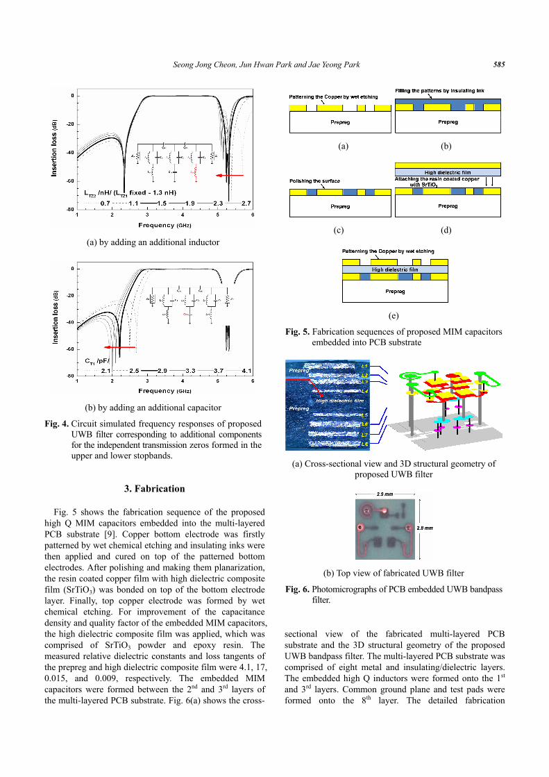
transmission zero at the upper and lower frequency stopband frequencies. In Fig. 3(a), the circuit parameters can be calculated from the input admittance
( ) ( ) 1/1/1
22
22
1 -
--
p
oL
LLB
ωωωω
ωω ⋅
+= (3)
where the series and parallel resonant frequencies, ωo and ωp are defined by
1 1 11/ , 1/ So pL C L Cω ω= = (4)
and the total inductance, LS is defined by
( )1 1/SL L L L L= + (5)
In case of ωp > ωo, such a two-port network being used
as a resonator in a filter structure provides a transmission zero at the real finite frequency, ωp situated in the upper stopband. On the other hand, the input admittance of the two-port network depicted in Fig. 3(b) can be written as
( )1/1/
22
22
-
-
p
oC CB
ωωωω
ωω = (6)
where the series and parallel resonant frequencies, ωo and ωp are defined by
( )2 2 2 21/ , 1/o pL C L C Cω ω= = + (7)
Consequently, a transmission zero was formed in the
lower stopband (ωp < ωo). Fig. 3 shows the circuit simulated scattering parameters corresponding to the additional passive components for forming the independent transmission zeros.
Fig. 4 illustrates the circuit simulated frequency responses of proposed UWB filter corresponding to additional components for forming independent transmission zeros. As shown in Fig. 4, each shunt resonator connected in series with the inductor or capacitor generated a finite transmission zero in the upper or lower stopbands, respectively. These transmission zeros were independent each other and controllable individually.
The optimized circuit parameters were transformed into the structural geometries by using 3D EM full-wave simulator. At this stage, the mutual parasitic coupling of the filter components in the compact multilayer structure would result in different simulation responses from those obtained initially. Therefore, the PCB layout was finally fine tuned to minimize the differences between the circuit and 3D EM full-wave based simulated results.
(a) by adding an additional inductor
(b) by adding an additional capacitor
Fig. 3. Depedency of circuit simulated scattered parameters of parallel resonant circuit on additional passive components for forming the independent transmission zeros.
Seong Jong Cheon, Jun Hwan Park and Jae Yeong Park
585
3. Fabrication Fig. 5 shows the fabrication sequence of the proposed
high Q MIM capacitors embedded into the multi-layered PCB substrate [9]. Copper bottom electrode was firstly patterned by wet chemical etching and insulating inks were then applied and cured on top of the patterned bottom electrodes. After polishing and making them planarization, the resin coated copper film with high dielectric composite film (SrTiO3) was bonded on top of the bottom electrode layer. Finally, top copper electrode was formed by wet chemical etching. For improvement of the capacitance density and quality factor of the embedded MIM capacitors, the high dielectric composite film was applied, which was comprised of SrTiO3 powder and epoxy resin. The measured relative dielectric constants and loss tangents of the prepreg and high dielectric composite film were 4.1, 17, 0.015, and 0.009, respectively. The embedded MIM capacitors were formed between the 2nd and 3rd layers of the multi-layered PCB substrate. Fig. 6(a) shows the cross-
sectional view of the fabricated multi-layered PCB substrate and the 3D structural geometry of the proposed UWB bandpass filter. The multi-layered PCB substrate was comprised of eight metal and insulating/dielectric layers. The embedded high Q inductors were formed onto the 1st and 3rd layers. Common ground plane and test pads were formed onto the 8th layer. The detailed fabrication
(a) by adding an additional inductor
(b) by adding an additional capacitor
Fig. 4. Circuit simulated frequency responses of proposedUWB filter corresponding to additional componentsfor the independent transmission zeros formed in the upper and lower stopbands.
(a) (b)
(c) (d)
(e)
Fig. 5. Fabrication sequences of proposed MIM capacitors embedded into PCB substrate
(a) Cross-sectional view and 3D structural geometry of proposed UWB filter
(b) Top view of fabricated UWB filter
Fig. 6. Photomicrographs of PCB embedded UWB bandpass filter.

Highly Miniaturized and Performed UWB Bandpass Filter Embedded into PCB with SrTiO3 Composite Layer
586
sequences of the embedded high Q inductors and PCB substrate was described in our previous works [8, 9]. Fig. 6(b) shows the photomicrograph of fully embedded UWB bandpass filter into the 8-layered PCB substrate. Its dimension was 2.9 x 2.8 x 0.55 (H) mm3, which was the smallest one compared with the previously published ones.
4. Experimental Results and Discussions The fabricated UWB bandpass filter have been measured
and characterized by using an HP 8510B network analyzer and two PICOPROBE coplanar ground-signal-ground (GSG) probes with a 250 um pitch size. And a short-open-load-through (SOLT) has been adopted to calibrate before measuring them.
For optimally designing the PCB embedded UWB bandpass filter, the embedded MIM capacitors were firstly fabricated, measured, and characterized. The overall quality factors of PCB embedded capacitors were higher than 20 in the passband ranged from 3.1 to 4.75 GHz. Fig. 7 shows the measured quality factor of the PCB embedded capacitor with the capacitance of 2.0 pF. The PCB embedded MIM capacitors also exhibited high linearity to their sizes and densities enough to apply for radio frequency circuits. The measured capacitance density was approximately12.2 pF/mm2.
Fig. 8 shows 3D EM simulated and measured frequency responses of the fabricated UWB bandpass filter. It exhibited the fractional bandwidth of about 51.6 % and insertion and return losses of 1.68 and 12 dB in passband. As expected, the formed transmission zeros were located at 2.2 and 5.15 GHz, resulting in excellent suppressions of 31 dB and 20 dB at the WLAN bands of 2.4 GHz and 5.15 GHz, respectively. While the measured suppression of lower out-of band ranged from 1 to 2.4 Hz was higher than 31 dB, it was higher than 18 dB at the frequencies ranged from 5.15 to 6 GHz. Most of simulated performance characteristics were well matched with the measured ones except for the upper transmission zero at 5.15 GHz. The discrepancy and performance degradation at the high frequencies over 5 GHz might be caused by the material properties of the utilized epoxy based PCB substrate. The measured group delay was less than 0.62 ns in the passband, as shown in Fig. 9.
5. Conclusions Highly miniaturized and fully embedded UWB (3.1 -
4.75GHz) bandpass filter has been newly designed, fabricated, and characterized by using lumped elements filter topology and hetero-structural PCB substrate with a high dielectric composite film layer. The 3rd order Chebyshev bandpass filter topology was adopted and modified to make it smaller and to improve its
performances by using J-inverter transformation technology. The J-inverter transformation technology was highly effective for embedding the filter circuit into the
Fig. 7. The measured capacitances and quality factors of the PCB embedded SrTiO3 composite MIM capacitor with the capacitance of 2.0 pF.
Fig. 8. Comparison of 3D EM simulated and measured frequency responses of fabricated UWB bandpass filter.
Fig. 9. Measured results of the insertion loss and group delay of fabricated UWB bandpass filter.

Seong Jong Cheon, Jun Hwan Park and Jae Yeong Park
587
PCB substrate and enhancing its performance. The proposed three independent transmission zeros were formed by adding an inductor or capacitor into the three shunt LC resonators. They were highly effective for improving the attenuation characteristics at the undesired frequency bands. Since these transmission zeros were independent each other, they were effective for designing the bandpass filters with small size, wide passband, and high attenuation characteristics. These design and fabrication technologies might be useful for advanced RF components and modules packaging with good performance characteristics, small size/volume, low cost, and high-level integrity.
Acknowledgements
This research was partially supported by Haedong
Science and Culture Foundation and SRC/ERC program of MOST/KOSEF (Intelligent Radio Engineering Center). The authors acknowledge Mr. H. S. Lee and Mr. S. G. Yoon of Daeduck Electronics and MiNDaP group members of Kwangwoon University for their technical supports and discussions.
References
[1] B. S. Kwon, S. S. Myoung, et al, “Co-planar
waveguide filter with ground perforation for ultra-wideband system,” Proceedings of Asia-Pacific Microwave Conference, vol. 3, pp. 1-4, Dec. 2005.
[2] Sheng Sun, Lei Zhu, et al, “A Compact Wideband Bandpass Filter Using Transversal Resonator and Asymmetrical Interdigital Coupled Lines,” IEEE Microwave and Wireless Components Letters, vol. 18, no. 3, 99. 173-175, Mar. 2008.
[3] L. K. Yeung and Ke-Li. Wu; “A compact Second-Order LTCC Bandpass Filter with Two Finite Transmission Zeros,” IEEE Transactions on Microwave Theory and Techniques, vol. 51, pp. 337-341, Feb. 2003.
[4] C-W. Tang, C-C. Tseng, et al, “Development of Ultra-wideband LTCC Filter,” IEEE International Conference on UWB, pp. 320-322, Sep. 2005.
[5] C-F. Chang and S-J. Chung, “Bandpass Filter of Serial Configuration with Two Finite Transmission Zeros using LTCC Technology,” IEEE Transactions on Microwave Theory and Techniques, vol. 53, pp. 2383-2388, Jul. 2005.
[6] C-W. Tang, T-C. Lin, C-Y. Chang, “Realization of Transmission Zeros in Combline Filters using an Auxiliary Inductively Coupled Ground Plane,” IEEE Transactions on Microwave Theory and Techniques, vol. 51, pp. 2112-2118, Oct. 2003.
[7] C. H. Chen and K. H. Lin, “Novel compact LTCC UWB bandpass filter with simple semi-lumped
circuit model,” International Conference on Microwave and Millimeter wave Technologies, vol. 1, pp. 21-24, Apr. 2008.
[8] J. C. Park and J. Y. Park, “Wideband LC Balun transformer using Coupled LC Resonators Embedded into Organic Substrate,” Microelectronics Journal, vol. 40, pp. 1555-1560, Nov. 2009.
[9] H-H Lee and J-Y Park, “Characterization of Fully Embedded RF Inductors in Organic SOP Technology,” IEEE Transactions on Advanced Packaging, vol. 32, No. 2, pp. 491-496, May 2009.
[10] R. R. Tummala and M. Swaminathan, Introduction to System-On-Package (SOP) Miniaturization of the Entire System, Chap. 7 SOP Substrate with Multilayer Wiring and Thin-Film Embedded Components, McGraw-Hill, New York, 2008.
[11] J. S. Hong and M. J. Lancaster, Microstrip Filters for RF/Microwave Applications, Chap. 3 Basic Concepts and theories of Filters, John Wiley&Sons, New York, 2001.
[12] G. Brzezina, L. Roy, L. MacEachern, “A miniature LTCC bandpass filter using novel resonators for GPS applications,” Proceedings of European Microwave Conference, pp. 536 – 539, Oct. 2007.
[13] J. S. Lim and D. C. Park, “A modified Chebyshev bandpass filter with attenuation poles in the stopband,” IEEE Transactions on Microwave Theory and Techniques, vol. 45, pp. 898–904, Jun. 1997.
[14] G. S. Yun and S. J. Kim, “Method of Fabricating an Embedded Capacitor in Printed Circuit Board,” Korea patent, 10-2008-0007502, 2008.
Seong-Jong Cheon He received the B.S. and M.S. degrees in Electronic Engineering from Kwangwoon Univer- sity, Seoul, Korea, in 2006 and 2008, respectively. He is currently working toward the Ph.D. degree in electronic engineering from Kwangwoon Univer- sity. His current research interests are
in the area of microelectronic devices, RF front-end modules, EPDs (Embedded Passive Devices), and SOP (System on Packaging).
Jun-Hwan Park He was born in Wonju, Korea, in 1982. He received his B.S. and M.S. degrees in electronic engineering from Kwangwoon Univer- sity, Seoul, Korea, in 2009 and 2011. He is currently working at Research and Division in Amkor technologies,
Ltd. His research interests include RF components and integrated front-ends.

Highly Miniaturized and Performed UWB Bandpass Filter Embedded into PCB with SrTiO3 Composite Layer
588
Jae-Yeong Park He received M.S.E.E. and Ph.D. degrees in Electrical and Computer Engineering from Georgia Institute of Technology in 1995 and 1997, respectively. After graduation, he worked at the Packaging Research Center of Georgia Institute of Techno- logy as a research engineer for 2 years.
He has also worked at Microsystem group in LG Electronics Institute of Technology as a Team leader of RF MEMS research for 6 years. In September 2004, he joined the faculty of department of Electronics Engineering in Kwangwoon University in Seoul, Korea. He has published more than 150 journal articles and conference proceedings and filed more than 90 patents. His current research interests include micro electro mechanical systems (MEMS, micro-actuators for optical and RF applications), micro- system packaging (wafer level packaging, micro solders, PCB embedded passives and modules, System on Packaging (SoP)), non enzymatic electrochemical sensors, smart dust, and RF MEMS components.


![Miniaturized UWB Microstrip Antenna for Microwave ImagingUWB applications, including medical imaging. This is due to their low profile, low cost and ease of integration [ 7]. This](https://img.pdfslide.net/doc/110x75/5e8813282ebce13d3976c277/miniaturized-uwb-microstrip-antenna-for-microwave-uwb-applications-including-medical.jpg)
![Development of Hexagonal MMR Based UWB Bandpass Filter ... · For such circumstances, a UWB filter is required to provide rejection capability in a band from 5 to 6 GHz [3-6].](https://img.pdfslide.net/doc/110x75/5e28116b7a0f7a70221dabdc/development-of-hexagonal-mmr-based-uwb-bandpass-filter-for-such-circumstances.jpg)