Embed Size (px)
Citation preview
40 JOURNAL OF DISPLAY TECHNOLOGY, VOL. 7, NO. 1, JANUARY 2011
Highly Transparent SU-8 Photoresist Barrier Rib fora Transparent AC Plasma Display Panel
Sung-Min Lee, Seung Hwa Oh, and Kyung Cheol Choi, Member, IEEE
Abstract—A highly transparent barrier rib was investigated foruse in a transparent ac plasma display panel. SU-8 photoresist isan appropriate material for a highly transparent barrier rib be-cause it absorbs only a small amount of light and provides a simplefabrication method for a rectangular barrier rib. SU-8 photoresistbarrier rib had a problem with reliability because it can be dam-aged by the plasma. Therefore, a silicon dioxide layer covered theSU-8 photoresist barrier rib for protection. Using this method, weobtained a highly transparent barrier rib with a long lifetime anda transmittance level of approximately 90%.
Index Terms—Barrier rib, plasma display panel (PDP), SU-8photoresist, transparent.
I. INTRODUCTION
A TRANSPARENT display is expected to be one of thepromising advanced information displays in the near fu-
ture [1], and [2], based on its applicability as a window dis-play that is less spatially constrained. Many researchers have,therefore, developed a transparent display using many displaytechnologies, such as organic light-emitting diodes (OLEDs)[3]–[6], inorganic light-emitting diodes (LEDs) [7], and micro-electromechanical systems (MEMS) [8]. Although these studiesshow the feasibility of the transparent display, its use is unattrac-tive for large displays compared to that of plasma display tech-nology because of the advantages of plasma display technology,such as easy fabrication and driving scheme [9]. Several groupshave attempted to develop a transparent display based on plasmadisplay technology. Lu et al. exhibited a transparent plasma dis-play with a microcavity structure [10]. Choi et al. reported atransparent ac plasma display panel (ac PDP) using alternativetransparent materials [11]. Lee et al. developed a transparent acPDP in which transparent glass barrier ribs were used [12], and[13]. These early attempts demonstrated the feasibility of thetransparent plasma display. However, further studies on highlytransparent components such as the dielectric, barrier rib, phos-phor, and electrode are required in order for the transparentplasma display to be realized practically.
In this study, a highly transparent barrier rib was investigated.SU-8 photoresist was proposed as an alternative transparent ma-
Manuscript received June 10, 2010; revised September 01, 2010; acceptedOctober 20, 2010. Date of current version January 14, 2011. This work wassupported in part by Basic Science Research Program through the NationalResearch Foundation of Korea (NRF) funded by the Ministry of Education,Science and Technology under CAFDC-20100009890 and in part by Informa-tion Display R&D Center under Grant F0004072-2010-33, one of the Knowl-edge Economy Frontier R&D Program funded by the Ministry of KnowledgeEconomy of Korean government.
The authors are with the Department of Electrical Engineering, KAIST, Dae-jeon, Republic of Korea Email: [email protected]
Color versions of one or more of the figures are available online at http://ieeexplore.ieee.org.
Digital Object Identifier 10.1109/JDT.2010.2089783
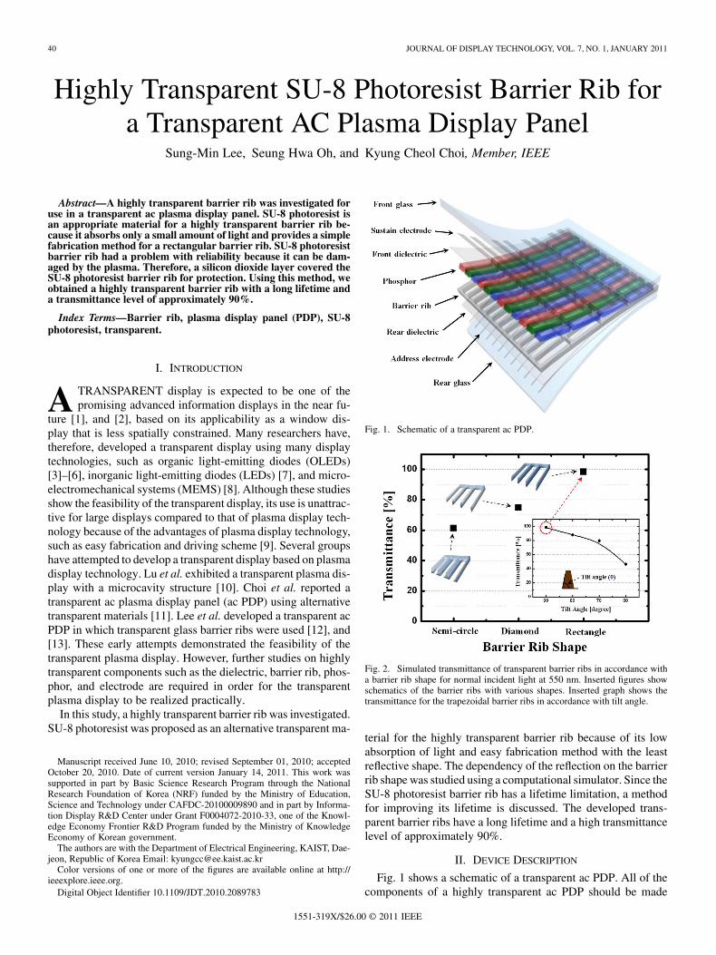
Fig. 1. Schematic of a transparent ac PDP.
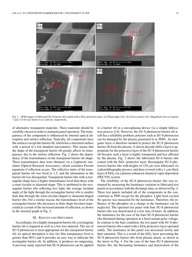
Fig. 2. Simulated transmittance of transparent barrier ribs in accordance witha barrier rib shape for normal incident light at 550 nm. Inserted figures showschematics of the barrier ribs with various shapes. Inserted graph shows thetransmittance for the trapezoidal barrier ribs in accordance with tilt angle.
terial for the highly transparent barrier rib because of its lowabsorption of light and easy fabrication method with the leastreflective shape. The dependency of the reflection on the barrierrib shape was studied using a computational simulator. Since theSU-8 photoresist barrier rib has a lifetime limitation, a methodfor improving its lifetime is discussed. The developed trans-parent barrier ribs have a long lifetime and a high transmittancelevel of approximately 90%.
II. DEVICE DESCRIPTION
Fig. 1 shows a schematic of a transparent ac PDP. All of thecomponents of a highly transparent ac PDP should be made
1551-319X/$26.00 © 2011 IEEE
LEE et al.: SU-8 PHOTORESIST BARRIER RIB FOR A TRANSPARENT AC PDP 41
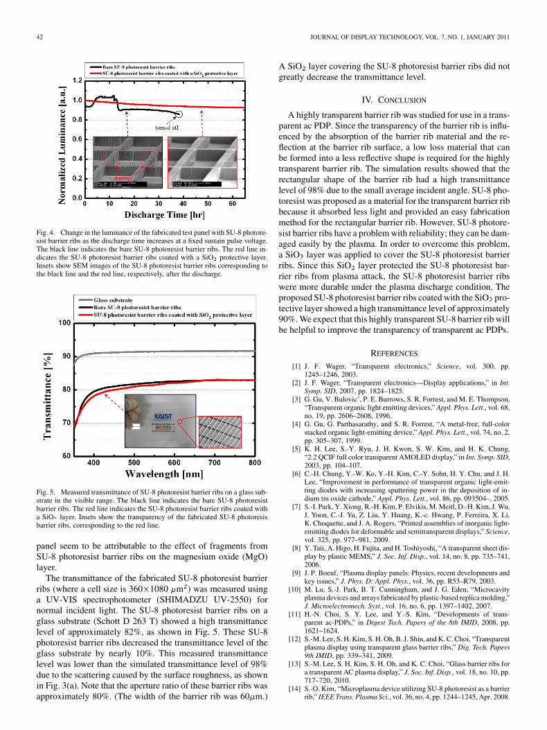
Fig. 3. SEM images of fabricated SU-8 barrier ribs coated with a SiO protective layer. (a) Tilted angle view. (b) Cross section view. Magnified views in regions1 and 2 of (b) are shown in (c) and (d), respectively.
of alternative transparent materials. These materials should becarefully chosen in order to maintain panel operation. The trans-parency of the component is influenced by internal optical ab-sorption and surface reflection. Typically, all components haveflat surfaces except the barrier rib, which has a structural surfacewith a period of a few hundred micrometers. This means thatthe shape of the transparent barrier rib greatly affects its trans-parency due to the surface reflection. Fig. 2 shows the depen-dency of the transmittance on the transparent barrier rib shape.These transmittance data were obtained via a Lighttools sim-ulator (Optical Research Associates), which considers Fresnelequations if reflection occurs. The reflective index of the trans-parent barrier rib was fixed to 1.5, and the attenuation in thebarrier rib was disregarded. Transparent barrier ribs with a rect-angular shape have a higher transmittance level than those witha semi-circular or diamond shape. This is attributed to the rect-angular barrier ribs reflecting less light; the average incidentangle of the light through the rectangular barrier ribs is smallerthan that through the semi-circular-shaped or diamond-shapedbarrier ribs. For a similar reason, the transmittance level of therectangular barrier ribs decreases as their shape becomes trape-zoidal as a result of the increased amount of reflection, as shownin the inserted graph in Fig. 2.
III. RESULTS AND DISCUSSION
Accordingly, for a highly transparent barrier rib, a rectangularbarrier rib is required as well as a low loss material. The use ofSU-8 photoresist is most appropriate for the transparent barrierrib; its optical absorption is low (its film transparency level isgreater than 90%) and it provides an easy way to fabricate therectangular barrier rib. In addition, it produces no outgassing.A previous study reported that SU-8 photoresist can be applied
to a barrier rib in a microplasma device via a simple fabrica-tion process [14]. However, the SU-8 photoresist barrier rib it-self has a reliability problem; polymer such as SU-8 photoresistcan be damaged by the plasma generated in ac PDPs. An inor-ganic layer is therefore needed to protect the SU-8 photoresistbarrier rib from the plasma. A silicon dioxide (SiO ) layer is ap-propriate for the protective layer of the SU-8 photoresist barrierrib because such a layer is highly transparent and less affectedby the plasma. Fig. 3 shows the fabricated SU-8 barrier ribscoated with the SiO protective layer. Rectangular SU-8 pho-toresist barrier ribs with heights of 120 m were fabricated viaa photolithography process, and then covered with a 1- m-thicklayer of SiO via a plasma-enhanced chemical vapor deposition(PECVD) system.
The reliability of the SU-8 photoresist barrier ribs was es-timated by measuring the luminance variation in fabricated testpanels in accordance with the discharge time, as shown in Fig. 4.These test panels included all of the components in the con-ventional ac PDP except for the phosphor. Light from excitedNe species was measured for the luminance. Therefore, the in-fluence of the phosphor on a change in the luminance can beneglected. The operated test panel with bare SU-8 photoresistbarrier ribs was deactivated in a few tens of hours. In addition,the luminance for the case of the bare SU-8 photoresist barrierribs fluctuated during operation at a fixed sustain pulse voltage.In contrast to the bare condition, the test panel with SU-8 pho-toresist barrier ribs coated with a SiO protective layer operatedstably. The luminance in this panel was decreased slowly andthen saturated. This is a result of the SiO layer preventing theSU-8 photoresist barrier ribs from plasma attack, as shown inthe insets in Fig. 4. For the case of the bare SU-8 photoresistbarrier ribs, the fluctuating luminance and deactivation of the
42 JOURNAL OF DISPLAY TECHNOLOGY, VOL. 7, NO. 1, JANUARY 2011
Fig. 4. Change in the luminance of the fabricated test panel with SU-8 photore-sist barrier ribs as the discharge time increases at a fixed sustain pulse voltage.The black line indicates the bare SU-8 photoresist barrier ribs. The red line in-dicates the SU-8 photoresist barrier ribs coated with a SiO protective layer.Insets show SEM images of the SU-8 photoresist barrier ribs corresponding tothe black line and the red line, respectively, after the discharge.
Fig. 5. Measured transmittance of SU-8 photoresist barrier ribs on a glass sub-strate in the visible range. The black line indicates the bare SU-8 photoresistbarrier ribs. The red line indicates the SU-8 photoresist barrier ribs coated witha SiO layer. Insets show the transparency of the fabricated SU-8 photoresisbarrier ribs, corresponding to the red line.
panel seem to be attributable to the effect of fragments fromSU-8 photoresist barrier ribs on the magnesium oxide (MgO)layer.
The transmittance of the fabricated SU-8 photoresist barrierribs (where a cell size is 360 1080 m ) was measured usinga UV-VIS spectrophotometer (SHIMADZU UV-2550) fornormal incident light. The SU-8 photoresist barrier ribs on aglass substrate (Schott D 263 T) showed a high transmittancelevel of approximately 82%, as shown in Fig. 5. These SU-8photoresist barrier ribs decreased the transmittance level of theglass substrate by nearly 10%. This measured transmittancelevel was lower than the simulated transmittance level of 98%due to the scattering caused by the surface roughness, as shownin Fig. 3(a). Note that the aperture ratio of these barrier ribs wasapproximately 80%. (The width of the barrier rib was 60 m.)
A SiO layer covering the SU-8 photoresist barrier ribs did notgreatly decrease the transmittance level.
IV. CONCLUSION
A highly transparent barrier rib was studied for use in a trans-parent ac PDP. Since the transparency of the barrier rib is influ-enced by the absorption of the barrier rib material and the re-flection at the barrier rib surface, a low loss material that canbe formed into a less reflective shape is required for the highlytransparent barrier rib. The simulation results showed that therectangular shape of the barrier rib had a high transmittancelevel of 98% due to the small average incident angle. SU-8 pho-toresist was proposed as a material for the transparent barrier ribbecause it absorbed less light and provided an easy fabricationmethod for the rectangular barrier rib. However, SU-8 photore-sist barrier ribs have a problem with reliability; they can be dam-aged easily by the plasma. In order to overcome this problem,a SiO layer was applied to cover the SU-8 photoresist barrierribs. Since this SiO layer protected the SU-8 photoresist bar-rier ribs from plasma attack, the SU-8 photoresist barrier ribswere more durable under the plasma discharge condition. Theproposed SU-8 photoresist barrier ribs coated with the SiO pro-tective layer showed a high transmittance level of approximately90%. We expect that this highly transparent SU-8 barrier rib willbe helpful to improve the transparency of transparent ac PDPs.
REFERENCES
[1] J. F. Wager, “Transparent electronics,” Science, vol. 300, pp.1245–1246, 2003.
[2] J. F. Wager, “Transparent electronics—Display applications,” in Int.Symp. SID, 2007, pp. 1824–1825.
[3] G. Gu, V. Bulovic’, P. E. Burrows, S. R. Forrest, and M. E. Thompson,“Transparent organic light emitting devices,” Appl. Phys. Lett., vol. 68,no. 19, pp. 2606–2608, 1996.
[4] G. Gu, G. Parthasarathy, and S. R. Forrest, “A metal-free, full-colorstacked organic light-emitting device,” Appl. Phys. Lett., vol. 74, no. 2,pp. 305–307, 1999.
[5] K. H. Lee, S.-Y. Ryu, J. H. Kwon, S. W. Kim, and H. K. Chung,“2.2 QCIF full color transparent AMOLED display,” in Int. Symp. SID,2003, pp. 104–107.
[6] C.-H. Chung, Y.-W. Ko, Y.-H. Kim, C.-Y. Sohn, H. Y. Chu, and J. H.Lee, “Improvement in performance of transparent organic light-emit-ting diodes with increasing sputtering power in the deposition of in-dium tin oxide cathode,” Appl. Phys. Lett., vol. 86, pp. 093504–, 2005.
[7] S.-I. Park, Y. Xiong, R.-H. Kim, P. Elvikis, M. Meitl, D.-H. Kim, J. Wu,J. Yoon, C.-J. Yu, Z. Liu, Y. Huang, K.-c. Hwang, P. Ferreira, X. Li,K. Choquette, and J. A. Rogers, “Printed assemblies of inorganic light-emitting diodes for deformable and semitransparent displays,” Science,vol. 325, pp. 977–981, 2009.
[8] Y. Taii, A. Higo, H. Fujita, and H. Toshiyoshi, “A transparent sheet dis-play by plastic MEMS,” J. Soc. Inf. Disp., vol. 14, no. 8, pp. 735–741,2006.
[9] J. P. Boeuf, “Plasma display panels: Physics, recent developments andkey issues,” J. Phys. D: Appl. Phys., vol. 36, pp. R53–R79, 2003.
[10] M. Lu, S.-J. Park, B. T. Cunningham, and J. G. Eden, “Microcavityplasma devices and arrays fabricated by plastic-based replica molding,”J. Microelectromech. Syst., vol. 16, no. 6, pp. 1397–1402, 2007.
[11] H.-N. Choi, S. Y. Lee, and Y.-S. Kim, “Developments of trans-parent ac-PDPs,” in Digest Tech. Papers of the 8th IMID, 2008, pp.1621–1624.
[12] S.-M. Lee, S. H. Kim, S. H. Oh, B. J. Shin, and K. C. Choi, “Transparentplasma display using transparent glass barrier ribs,” Dig. Tech. Papers9th IMID, pp. 339–341, 2009.
[13] S.-M. Lee, S. H. Kim, S. H. Oh, and K. C. Choi, “Glass barrier ribs fora transparent AC plasma display,” J. Soc. Inf. Disp., vol. 18, no. 10, pp.717–720, 2010.
[14] S.-O. Kim, “Microplasma device utilizing SU-8 photoresist as a barrierrib,” IEEE Trans. Plasma Sci., vol. 36, no. 4, pp. 1244–1245, Apr. 2008.
LEE et al.: SU-8 PHOTORESIST BARRIER RIB FOR A TRANSPARENT AC PDP 43
Sung-Min Lee received the B.S. degree in electricalengineering from Seoul National University, Seoul,Korea, in 2006 and the M.S. degree in electrical engi-neering from KAIST, Daejeon, Korea, in 2008, wherehe is currently working toward the Ph.D. degree inelectrical engineering.
His research interests include display devices andplasmonic devices.
Seung Hwa Oh received the B.S. degree in electricalengineering from KAIST, Daejeon, Korea, in 2009,where he is currently working toward the M.S. degreein electrical engineering.
His research interests include transparent displaydevices using plasmon.
Kyung Cheol Choi (M’04) received the B.S. degreefrom the Department of Electrical Engineering, SeoulNational University, Seoul, Korea, in 1986, and theM.S. degree and Ph.D. degree in plasma engineeringfrom Seoul National University in 1988 and 1993,respectively.
From 1993 to 1995, he was with the Institutefor Advanced Engineering, Seoul, where his workfocused on the design of display devices. From 1995to 1996, he was a Research Scientist with SpectronCorporation of America, Summit, NJ. From 1996
to 1998, he was a Senior Research Scientist with Hyundai Plasma Display,Hawthorne, NY. From 1998 to 1999, he was a Senior Research Scientistwith the Advanced Display R&D Center, Hyundai Electronics Industries,Gyounggi-do, Korea, where he was involved in the development of a 40-in acPDP. From 2000 to 2004, he was an Associate Professor with the Departmentof Electronics Engineering, Sejong University, Seoul. He was also in charge ofthe Information Display Research Center supported by the Korean Ministry ofInformation and Communication. Since 2005, he has been with the Departmentof Electrical Engineering, KAIST, Daejeon, Korea, where he was first anAssociate Professor and is currently a Professor. Since September 2007, hehas been in charge of the Center for Advanced Flexible Display Convergencesupported by the Korean Ministry of Education, Science, and Technology.His research interests include flexible displays, plasma display panels, organiclight-emitting diodes, and surface plasmon applications for displays.
Dr. Choi is a member of the Society for Information Display and the Ko-rean Information Display Society. He is an Associate Editor of the IEEE/OSAJOURNAL OF DISPLAY TECHNOLOGY.