Embed Size (px)
Citation preview

FN3659 Rev 8.00 Page 1 of 17September 15, 2015
FN3659Rev 8.00
September 15, 2015
HIP4081A80V/2.5A Peak, High Frequency Full Bridge FET Driver
DATASHEET
The HIP4081A is a high frequency, medium voltage Full Bridge N-Channel FET driver IC, available in 20 lead plastic SOIC and DIP packages. The HIP4081A can drive every possible switch combination except those which would cause a shoot-through condition. The HIP4081A can switch at frequencies up to 1MHz and is well suited to driving Voice Coil Motors, high-frequency switching power amplifiers, and power supplies.
For example, the HIP4081A can drive medium voltage brush motors, and two HIP4081As can be used to drive high performance stepper motors, since the short minimum “on-time” can provide fine micro-stepping capability.
Short propagation delays of approximately 55ns maximizes control loop crossover frequencies and dead-times which can be adjusted to near zero to minimize distortion, resulting in rapid, precise control of the driven load.
A similar part, the HIP4080A, includes an on-chip input comparator to create a PWM signal from an external triangle wave and to facilitate “hysteresis mode” switching.
The Application Note for the HIP4081A is the AN9405.
Features
• Independently Drives 4 N-Channel FET in Half Bridge or Full Bridge Configurations
• Bootstrap Supply Max Voltage to 95VDC
• Drives 1000pF Load at 1MHz in Free Air at 50°C with Rise and Fall Times of Typically 10ns
• User-Programmable Dead Time
• On-Chip Charge-Pump and Bootstrap Upper Bias Supplies
• DIS (Disable) Overrides Input Control
• Input Logic Thresholds Compatible with 5V to 15V Logic Levels
• Very Low Power Consumption
• Undervoltage Protection
• Pb-free Available
Applications
• Medium/Large Voice Coil Motors
• Full Bridge Power Supplies
• Switching Power Amplifiers
• High Performance Motor Controls
• Noise Cancellation Systems
• Battery Powered Vehicles
• Peripherals
• U.P.S.
PinoutHIP4081A
(PDIP, SOIC)TOP VIEW
Ordering Information
PARTNUMBER
TEMPRANGE
(°C) PACKAGEPKG.
DWG. #
HIP4081AIP (No longer available, recommended replacement: HIP4081AIPZ)
-40 to 85 20 Ld PDIP E20.3
HIP4081AIPZ (Note) -40 to 85 20 Ld PDIP(Pb-free)
E20.3
HIP4081AIB -40 to 85 20 Ld SOIC (W) M20.3
HIP4081AIBZ (Note) -40 to 85 20 Ld SOIC (W)(Pb-free)
M20.3
NOTE: Intersil Pb-free products employ special Pb-free material sets; molding compounds/die attach materials and 100% matte tin plate termination finish, which is compatible with both SnPb and Pb-free soldering operations. Intersil Pb-free products are MSL classified at Pb-free peak reflow temperatures that meet or exceed the Pb-free requirements of IPC/JEDEC J Std-020B.
11
12
13
14
15
16
17
18
20
19
10
9
8
7
6
5
4
3
2
1BHB
BHI
DIS
VSS
BLI
ALI
HDEL
AHI
LDEL
AHB
BHO
BLO
BLS
VDD
BHS
VCC
ALS
ALO
AHS
AHO

HIP4081A
Application Block Diagram
Functional Block Diagram (1/2 HIP4081A)
80V
GND
LOAD
HIP4081A
GND
12V
AHI
ALI
BLI
BHI BLO
BHS
BHO
ALO
AHS
AHO
CHARGEPUMP
VDD
AHI
DIS
ALI
HDEL
LDEL
VSS
TURN-ONDELAY
TURN-ONDELAY
DRIVER
DRIVER
AHB
AHO
AHS
VCC
ALO
ALSCBF
TO VDD (PIN 16)
CBS
DBS
HIGH VOLTAGE BUS 80VDC
+12VDC
LEVEL SHIFTAND LATCH
14
10
11
12
15
13
16
7
3
6
8
9
4
BIASSUPPLY
UNDER-VOLTAGE
FN3659 Rev 8.00 Page 2 of 17September 15, 2015
HIP4081A
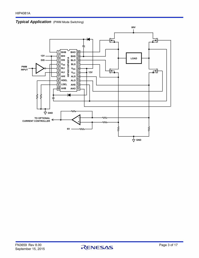
Typical Application (PWM Mode Switching)
11
12
13
14
15
16
17
18
20
19
10
9
8
7
6
5
4
3
2
1 BHB
BHI
DIS
VSS
BLI
ALI
HDEL
AHI
LDEL
AHB
BHO
BLO
BLS
VDD
BHS
VCC
ALS
ALO
AHS
AHO
80V
12V
+
-
12V
DIS
GND
6V
GND
TO OPTIONALCURRENT CONTROLLER
PWM
LOAD
INPUTH
IP4
08
1/H
IP4
081
A
FN3659 Rev 8.00 Page 3 of 17September 15, 2015
HIP4081A
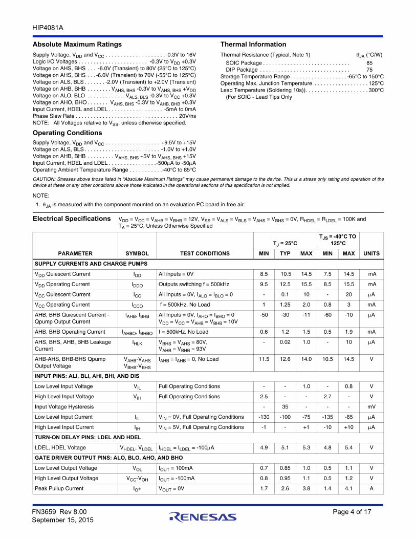
Absolute Maximum Ratings Thermal Information
Supply Voltage, VDD and VCC . . . . . . . . . . . . . . . . . . . . -0.3V to 16VLogic I/O Voltages . . . . . . . . . . . . . . . . . . . . . . . -0.3V to VDD +0.3VVoltage on AHS, BHS . . . -6.0V (Transient) to 80V (25°C to 125°C)Voltage on AHS, BHS . . . -6.0V (Transient) to 70V (-55°C to 125°C)Voltage on ALS, BLS . . . . . . . -2.0V (Transient) to +2.0V (Transient)Voltage on AHB, BHB . . . . . . . . VAHS, BHS -0.3V to VAHS, BHS +VDDVoltage on ALO, BLO . . . . . . . . . . . . .VALS, BLS -0.3V to VCC +0.3VVoltage on AHO, BHO . . . . . . . VAHS, BHS -0.3V to VAHB, BHB +0.3VInput Current, HDEL and LDEL . . . . . . . . . . . . . . . . . . -5mA to 0mAPhase Slew Rate . . . . . . . . . . . . . . . . . . . . . . . . . . . . . . . . . . 20V/nsNOTE: All Voltages relative to VSS, unless otherwise specified.
Thermal Resistance (Typical, Note 1) JA (°C/W)
SOIC Package . . . . . . . . . . . . . . . . . . . . . . . . . . . . . 85DIP Package . . . . . . . . . . . . . . . . . . . . . . . . . . . . . . 75
Storage Temperature Range . . . . . . . . . . . . . . . . . . . -65°C to 150°COperating Max. Junction Temperature . . . . . . . . . . . . . . . . . . 125°CLead Temperature (Soldering 10s)). . . . . . . . . . . . . . . . . . . . . 300°C
(For SOIC - Lead Tips Only
Operating ConditionsSupply Voltage, VDD and VCC . . . . . . . . . . . . . . . . . . +9.5V to +15VVoltage on ALS, BLS . . . . . . . . . . . . . . . . . . . . . . . . . -1.0V to +1.0VVoltage on AHB, BHB . . . . . . . . . VAHS, BHS +5V to VAHS, BHS +15VInput Current, HDEL and LDEL . . . . . . . . . . . . . . . .-500A to -50AOperating Ambient Temperature Range . . . . . . . . . . .-40°C to 85°C
CAUTION: Stresses above those listed in “Absolute Maximum Ratings” may cause permanent damage to the device. This is a stress only rating and operation of thedevice at these or any other conditions above those indicated in the operational sections of this specification is not implied.
NOTE:
1. JA is measured with the component mounted on an evaluation PC board in free air.
Electrical Specifications VDD = VCC = VAHB = VBHB = 12V, VSS = VALS = VBLS = VAHS = VBHS = 0V, RHDEL = RLDEL = 100K and TA = 25°C, Unless Otherwise Specified
PARAMETER SYMBOL TEST CONDITIONS
TJ = 25°CTJS = -40°C TO
125°C
UNITSMIN TYP MAX MIN MAX
SUPPLY CURRENTS AND CHARGE PUMPS
VDD Quiescent Current IDD All inputs = 0V 8.5 10.5 14.5 7.5 14.5 mA
VDD Operating Current IDDO Outputs switching f = 500kHz 9.5 12.5 15.5 8.5 15.5 mA
VCC Quiescent Current ICC All Inputs = 0V, IALO = IBLO = 0 - 0.1 10 - 20 A
VCC Operating Current ICCO f = 500kHz, No Load 1 1.25 2.0 0.8 3 mA
AHB, BHB Quiescent Current -Qpump Output Current
IAHB, IBHB All Inputs = 0V, IAHO = IBHO = 0VDD = VCC = VAHB = VBHB = 10V
-50 -30 -11 -60 -10 A
AHB, BHB Operating Current IAHBO, IBHBO f = 500kHz, No Load 0.6 1.2 1.5 0.5 1.9 mA
AHS, BHS, AHB, BHB Leakage Current
IHLK VBHS = VAHS = 80V,VAHB = VBHB = 93V
- 0.02 1.0 - 10 A
AHB-AHS, BHB-BHS Qpump Output Voltage
VAHB-VAHSVBHB-VBHS
IAHB = IAHB = 0, No Load 11.5 12.6 14.0 10.5 14.5 V
INPUT PINS: ALI, BLI, AHI, BHI, AND DIS
Low Level Input Voltage VIL Full Operating Conditions - - 1.0 - 0.8 V
High Level Input Voltage VIH Full Operating Conditions 2.5 - - 2.7 - V
Input Voltage Hysteresis - 35 - - - mV
Low Level Input Current IIL VIN = 0V, Full Operating Conditions -130 -100 -75 -135 -65 A
High Level Input Current IIH VIN = 5V, Full Operating Conditions -1 - +1 -10 +10 A
TURN-ON DELAY PINS: LDEL AND HDEL
LDEL, HDEL Voltage VHDEL, VLDEL IHDEL = ILDEL = -100A 4.9 5.1 5.3 4.8 5.4 V
GATE DRIVER OUTPUT PINS: ALO, BLO, AHO, AND BHO
Low Level Output Voltage VOL IOUT = 100mA 0.7 0.85 1.0 0.5 1.1 V
High Level Output Voltage VCC-VOH IOUT = -100mA 0.8 0.95 1.1 0.5 1.2 V
Peak Pullup Current IO+ VOUT = 0V 1.7 2.6 3.8 1.4 4.1 A
FN3659 Rev 8.00 Page 4 of 17September 15, 2015
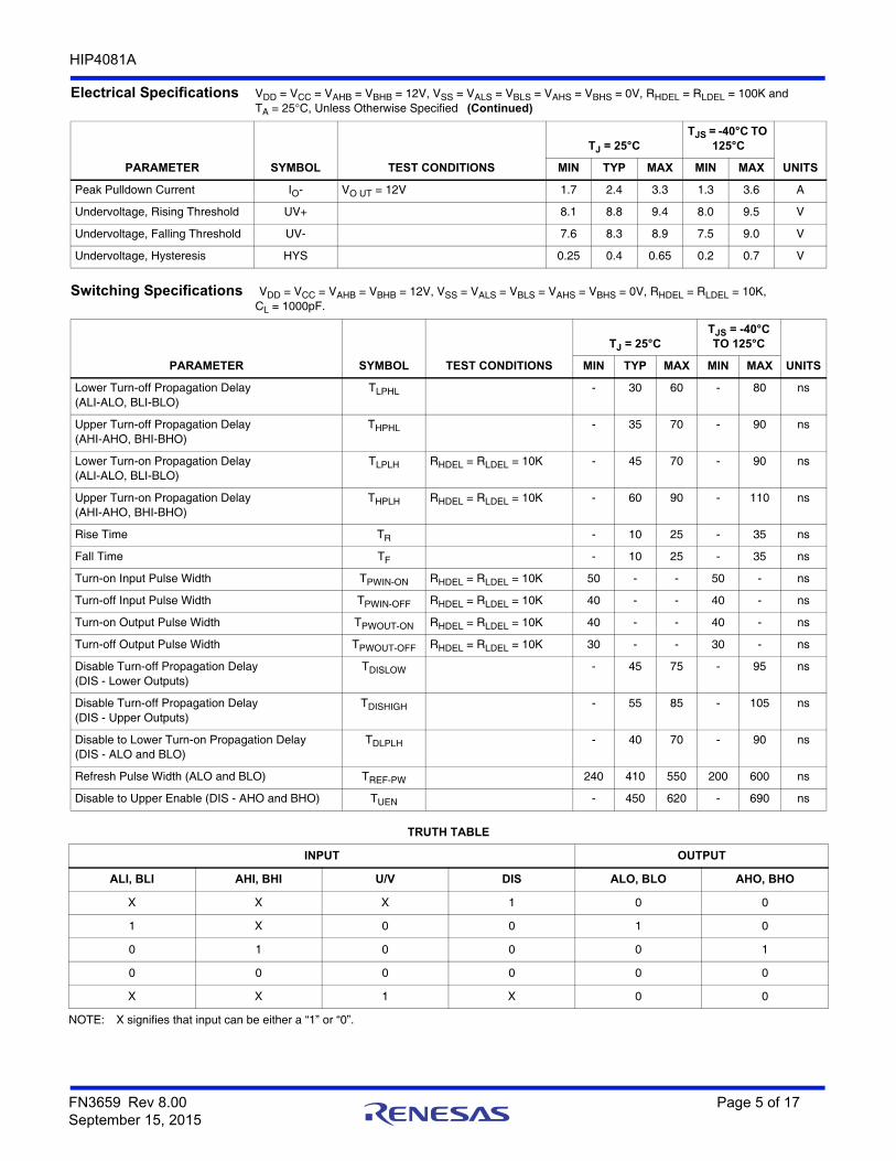
HIP4081A
Peak Pulldown Current IO- VO UT = 12V 1.7 2.4 3.3 1.3 3.6 A
Undervoltage, Rising Threshold UV+ 8.1 8.8 9.4 8.0 9.5 V
Undervoltage, Falling Threshold UV- 7.6 8.3 8.9 7.5 9.0 V
Undervoltage, Hysteresis HYS 0.25 0.4 0.65 0.2 0.7 V
Switching Specifications VDD = VCC = VAHB = VBHB = 12V, VSS = VALS = VBLS = VAHS = VBHS = 0V, RHDEL = RLDEL = 10K,CL = 1000pF.
PARAMETER SYMBOL TEST CONDITIONS
TJ = 25°CTJS = -40°C TO 125°C
UNITSMIN TYP MAX MIN MAX
Lower Turn-off Propagation Delay(ALI-ALO, BLI-BLO)
TLPHL - 30 60 - 80 ns
Upper Turn-off Propagation Delay(AHI-AHO, BHI-BHO)
THPHL - 35 70 - 90 ns
Lower Turn-on Propagation Delay(ALI-ALO, BLI-BLO)
TLPLH RHDEL = RLDEL = 10K - 45 70 - 90 ns
Upper Turn-on Propagation Delay(AHI-AHO, BHI-BHO)
THPLH RHDEL = RLDEL = 10K - 60 90 - 110 ns
Rise Time TR - 10 25 - 35 ns
Fall Time TF - 10 25 - 35 ns
Turn-on Input Pulse Width TPWIN-ON RHDEL = RLDEL = 10K 50 - - 50 - ns
Turn-off Input Pulse Width TPWIN-OFF RHDEL = RLDEL = 10K 40 - - 40 - ns
Turn-on Output Pulse Width TPWOUT-ON RHDEL = RLDEL = 10K 40 - - 40 - ns
Turn-off Output Pulse Width TPWOUT-OFF RHDEL = RLDEL = 10K 30 - - 30 - ns
Disable Turn-off Propagation Delay(DIS - Lower Outputs)
TDISLOW - 45 75 - 95 ns
Disable Turn-off Propagation Delay(DIS - Upper Outputs)
TDISHIGH - 55 85 - 105 ns
Disable to Lower Turn-on Propagation Delay(DIS - ALO and BLO)
TDLPLH - 40 70 - 90 ns
Refresh Pulse Width (ALO and BLO) TREF-PW 240 410 550 200 600 ns
Disable to Upper Enable (DIS - AHO and BHO) TUEN - 450 620 - 690 ns
TRUTH TABLE
INPUT OUTPUT
ALI, BLI AHI, BHI U/V DIS ALO, BLO AHO, BHO
X X X 1 0 0
1 X 0 0 1 0
0 1 0 0 0 1
0 0 0 0 0 0
X X 1 X 0 0
NOTE: X signifies that input can be either a “1” or “0”.
Electrical Specifications VDD = VCC = VAHB = VBHB = 12V, VSS = VALS = VBLS = VAHS = VBHS = 0V, RHDEL = RLDEL = 100K and TA = 25°C, Unless Otherwise Specified (Continued)
PARAMETER SYMBOL TEST CONDITIONS
TJ = 25°CTJS = -40°C TO
125°C
UNITSMIN TYP MAX MIN MAX
FN3659 Rev 8.00 Page 5 of 17September 15, 2015
HIP4081A
FN3659 Rev 8.00 Page 6 of 17September 15, 2015
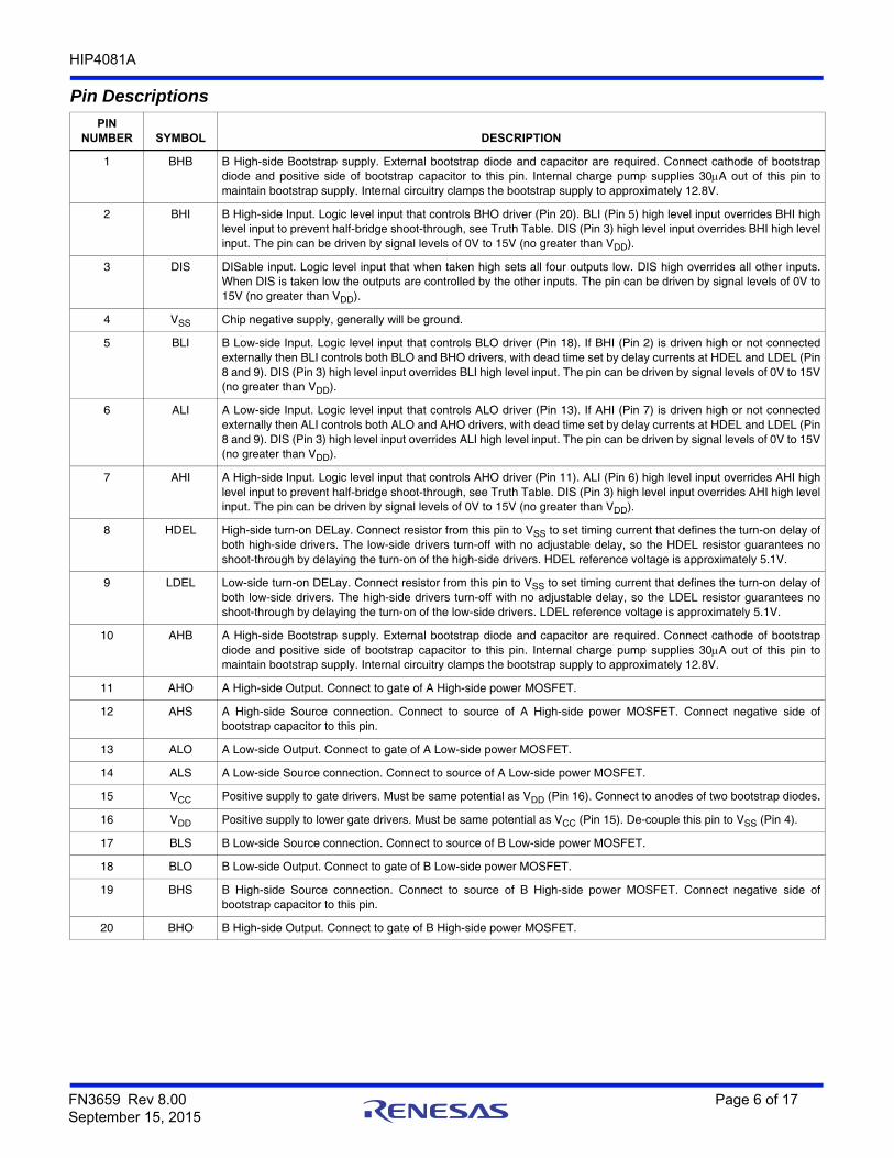
Pin Descriptions
PINNUMBER SYMBOL DESCRIPTION
1 BHB B High-side Bootstrap supply. External bootstrap diode and capacitor are required. Connect cathode of bootstrapdiode and positive side of bootstrap capacitor to this pin. Internal charge pump supplies 30A out of this pin tomaintain bootstrap supply. Internal circuitry clamps the bootstrap supply to approximately 12.8V.
2 BHI B High-side Input. Logic level input that controls BHO driver (Pin 20). BLI (Pin 5) high level input overrides BHI highlevel input to prevent half-bridge shoot-through, see Truth Table. DIS (Pin 3) high level input overrides BHI high levelinput. The pin can be driven by signal levels of 0V to 15V (no greater than VDD).
3 DIS DISable input. Logic level input that when taken high sets all four outputs low. DIS high overrides all other inputs.When DIS is taken low the outputs are controlled by the other inputs. The pin can be driven by signal levels of 0V to15V (no greater than VDD).
4 VSS Chip negative supply, generally will be ground.
5 BLI B Low-side Input. Logic level input that controls BLO driver (Pin 18). If BHI (Pin 2) is driven high or not connectedexternally then BLI controls both BLO and BHO drivers, with dead time set by delay currents at HDEL and LDEL (Pin8 and 9). DIS (Pin 3) high level input overrides BLI high level input. The pin can be driven by signal levels of 0V to 15V(no greater than VDD).
6 ALI A Low-side Input. Logic level input that controls ALO driver (Pin 13). If AHI (Pin 7) is driven high or not connectedexternally then ALI controls both ALO and AHO drivers, with dead time set by delay currents at HDEL and LDEL (Pin8 and 9). DIS (Pin 3) high level input overrides ALI high level input. The pin can be driven by signal levels of 0V to 15V(no greater than VDD).
7 AHI A High-side Input. Logic level input that controls AHO driver (Pin 11). ALI (Pin 6) high level input overrides AHI highlevel input to prevent half-bridge shoot-through, see Truth Table. DIS (Pin 3) high level input overrides AHI high levelinput. The pin can be driven by signal levels of 0V to 15V (no greater than VDD).
8 HDEL High-side turn-on DELay. Connect resistor from this pin to VSS to set timing current that defines the turn-on delay ofboth high-side drivers. The low-side drivers turn-off with no adjustable delay, so the HDEL resistor guarantees noshoot-through by delaying the turn-on of the high-side drivers. HDEL reference voltage is approximately 5.1V.
9 LDEL Low-side turn-on DELay. Connect resistor from this pin to VSS to set timing current that defines the turn-on delay ofboth low-side drivers. The high-side drivers turn-off with no adjustable delay, so the LDEL resistor guarantees noshoot-through by delaying the turn-on of the low-side drivers. LDEL reference voltage is approximately 5.1V.
10 AHB A High-side Bootstrap supply. External bootstrap diode and capacitor are required. Connect cathode of bootstrapdiode and positive side of bootstrap capacitor to this pin. Internal charge pump supplies 30A out of this pin tomaintain bootstrap supply. Internal circuitry clamps the bootstrap supply to approximately 12.8V.
11 AHO A High-side Output. Connect to gate of A High-side power MOSFET.
12 AHS A High-side Source connection. Connect to source of A High-side power MOSFET. Connect negative side ofbootstrap capacitor to this pin.
13 ALO A Low-side Output. Connect to gate of A Low-side power MOSFET.
14 ALS A Low-side Source connection. Connect to source of A Low-side power MOSFET.
15 VCC Positive supply to gate drivers. Must be same potential as VDD (Pin 16). Connect to anodes of two bootstrap diodes.
16 VDD Positive supply to lower gate drivers. Must be same potential as VCC (Pin 15). De-couple this pin to VSS (Pin 4).
17 BLS B Low-side Source connection. Connect to source of B Low-side power MOSFET.
18 BLO B Low-side Output. Connect to gate of B Low-side power MOSFET.
19 BHS B High-side Source connection. Connect to source of B High-side power MOSFET. Connect negative side ofbootstrap capacitor to this pin.
20 BHO B High-side Output. Connect to gate of B High-side power MOSFET.
HIP4081A
FN3659 Rev 8.00 Page 7 of 17September 15, 2015
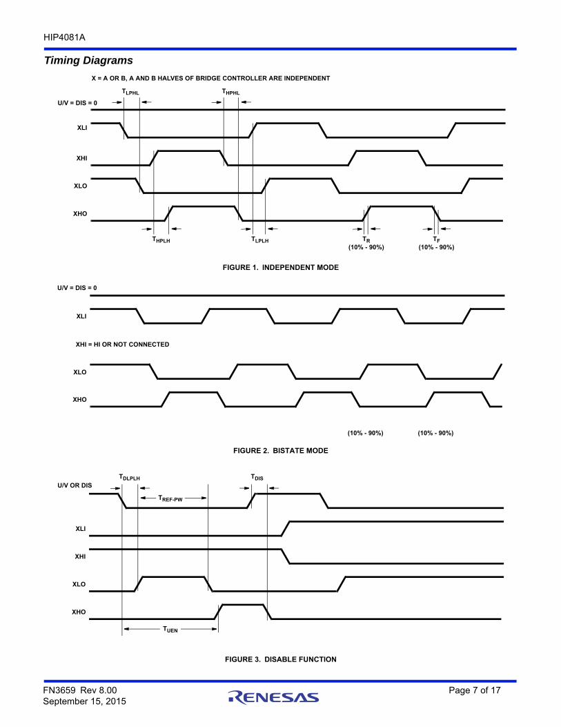
Timing Diagrams
FIGURE 1. INDEPENDENT MODE
FIGURE 2. BISTATE MODE
FIGURE 3. DISABLE FUNCTION
U/V = DIS = 0
XLI
XHI
XLO
XHO
TLPHL THPHL
THPLH TLPLH TR(10% - 90%)
TF(10% - 90%)
X = A OR B, A AND B HALVES OF BRIDGE CONTROLLER ARE INDEPENDENT
U/V = DIS = 0
XLI
XHI = HI OR NOT CONNECTED
XLO
XHO
(10% - 90%) (10% - 90%)
U/V OR DIS
XLI
XHI
XLO
XHO
TDLPLH TDIS
TUEN
TREF-PW
HIP4081A
FN3659 Rev 8.00 Page 8 of 17September 15, 2015
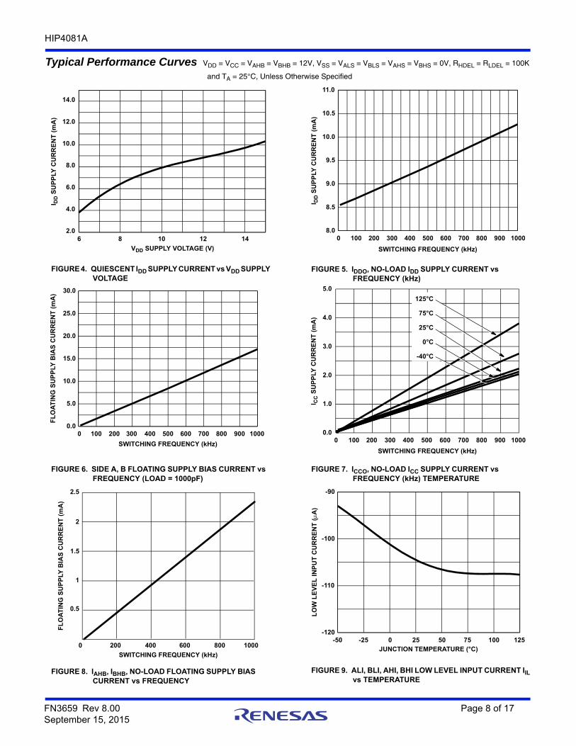
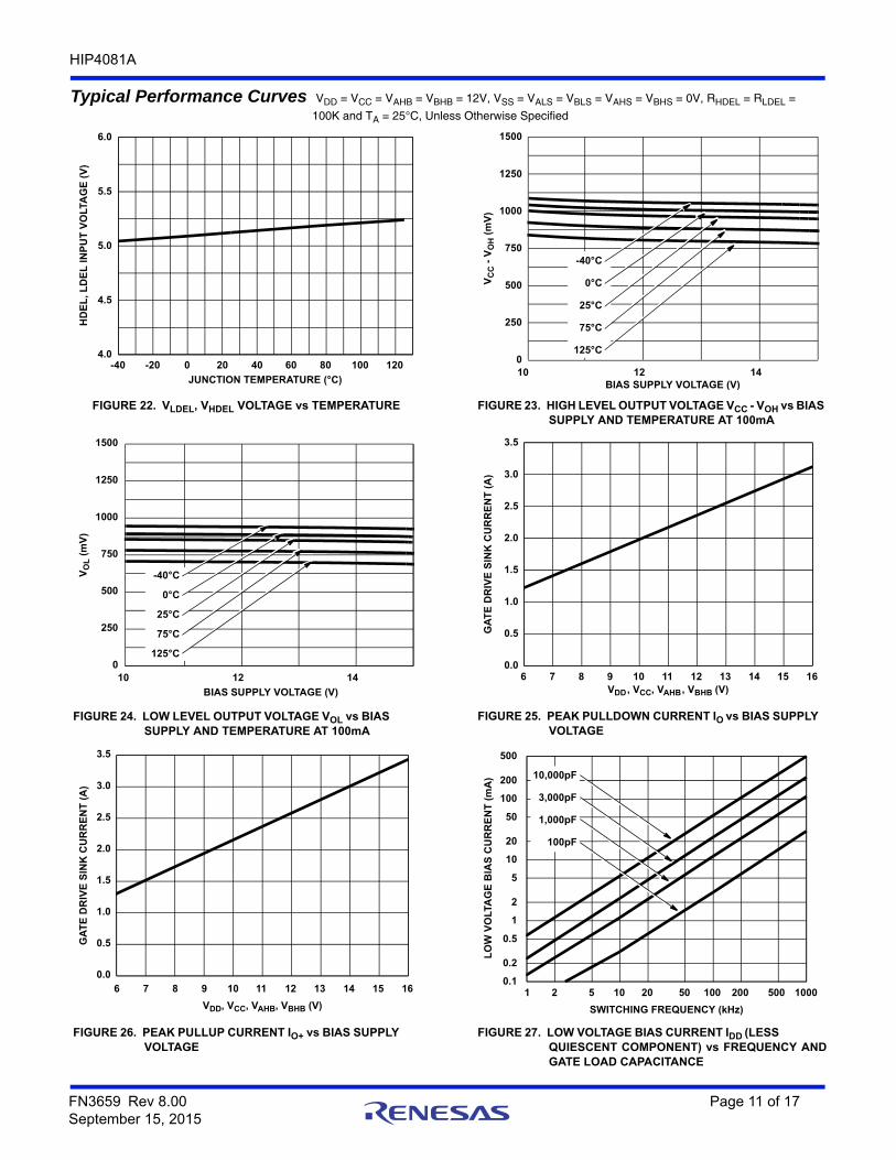
Typical Performance Curves VDD = VCC = VAHB = VBHB = 12V, VSS = VALS = VBLS = VAHS = VBHS = 0V, RHDEL = RLDEL = 100K
and TA = 25°C, Unless Otherwise Specified
FIGURE 4. QUIESCENT IDD SUPPLY CURRENT vs VDD SUPPLY VOLTAGE
FIGURE 5. IDDO, NO-LOAD IDD SUPPLY CURRENT vs FREQUENCY (kHz)
FIGURE 6. SIDE A, B FLOATING SUPPLY BIAS CURRENT vs FREQUENCY (LOAD = 1000pF)
FIGURE 7. ICCO, NO-LOAD ICC SUPPLY CURRENT vs FREQUENCY (kHz) TEMPERATURE
FIGURE 8. IAHB, IBHB, NO-LOAD FLOATING SUPPLY BIAS CURRENT vs FREQUENCY
FIGURE 9. ALI, BLI, AHI, BHI LOW LEVEL INPUT CURRENT IIL vs TEMPERATURE
6 8 10 12 142.0
4.0
6.0
8.0
10.0
12.0
14.0
I DD
SU
PP
LY C
UR
RE
NT
(m
A)
VDD SUPPLY VOLTAGE (V)
0 100 200 300 400 500 600 700 800 900 10008.0
8.5
9.0
9.5
10.0
10.5
11.0
I DD
SU
PP
LY C
UR
RE
NT
(m
A)
SWITCHING FREQUENCY (kHz)
0 100 200 300 400 500 600 700 800 900 10000.0
5.0
10.0
15.0
20.0
25.0
30.0
FL
OA
TIN
G S
UP
PLY
BIA
S C
UR
RE
NT
(m
A)
SWITCHING FREQUENCY (kHz)0 100 200 300 400 500 600 700 800 900 1000
0.0
1.0
2.0
3.0
4.0
5.0
I CC
SU
PP
LY C
UR
RE
NT
(m
A)
SWITCHING FREQUENCY (kHz)
75°C
25°C
125°C
-40°C
0°C
0.5
1
1.5
2
2.5
200 600 800 10000 400
FL
OA
TIN
G S
UP
PLY
BIA
S C
UR
RE
NT
(m
A)
SWITCHING FREQUENCY (kHz)
-50 -25 0 25 50 75 100 125-120
-110
-100
-90
LO
W L
EV
EL
IN
PU
T C
UR
RE
NT
(A
)
JUNCTION TEMPERATURE (°C)
HIP4081A
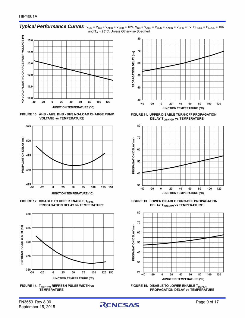
Typical Performance Curves VDD = VCC = VAHB = VBHB = 12V, VSS = VALS = VBLS = VAHS = VBHS = 0V, RHDEL = RLDEL = 10K and TA = 25°C, Unless Otherwise Specified
FIGURE 10. AHB - AHS, BHB - BHS NO-LOAD CHARGE PUMP VOLTAGE vs TEMPERATURE
FIGURE 11. UPPER DISABLE TURN-OFF PROPAGATION DELAY TDISHIGH vs TEMPERATURE
FIGURE 12. DISABLE TO UPPER ENABLE, TUEN, PROPAGATION DELAY vs TEMPERATURE
FIGURE 13. LOWER DISABLE TURN-OFF PROPAGATION DELAY TDISLOW vs TEMPERATURE
FIGURE 14. TREF-PW REFRESH PULSE WIDTH vs TEMPERATURE
FIGURE 15. DISABLE TO LOWER ENABLE TDLPLH PROPAGATION DELAY vs TEMPERATURE
-40 -20 0 20 40 60 80 100 12010.0
11.0
12.0
13.0
14.0
15.0
NO
-LO
AD
FL
OA
TIN
G C
HA
RG
E P
UM
P V
OLT
AG
E (
V)
JUNCTION TEMPERATURE (°C)-40 -20 0 20 40 60 80 100 120
30
40
50
60
70
80
PR
OP
AG
AT
ION
DE
LA
Y (
ns
)
JUNCTION TEMPERATURE (°C)
425
450
475
500
525
-50 -25 0 25 50 75 100 125 150
JUNCTION TEMPERATURE (°C)
PR
OP
AG
AT
ION
DE
LA
Y (
ns
)
-40 -20 0 20 40 60 80 100 12030
40
50
60
70
80
PR
OP
AG
AT
ION
DE
LA
Y (
ns
)
JUNCTION TEMPERATURE (°C)
350
375
400
425
450
-50 -25 0 25 50 75 100 125 150
RE
FR
ES
H P
UL
SE
WID
TH
(n
s)
JUNCTION TEMPERATURE (°C)
-40 -20 0 20 40 60 80 100 12020
30
40
50
60
70
80
PR
OP
AG
AT
ION
DE
LA
Y (
ns
)
JUNCTION TEMPERATURE (°C)
FN3659 Rev 8.00 Page 9 of 17September 15, 2015
HIP4081A
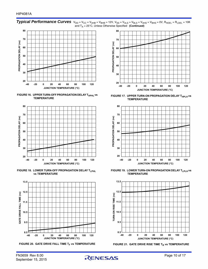
FIGURE 16. UPPER TURN-OFF PROPAGATION DELAY THPHL vs TEMPERATURE
FIGURE 17. UPPER TURN-ON PROPAGATION DELAY THPLH vs TEMPERATURE
FIGURE 18. LOWER TURN-OFF PROPAGATION DELAY TLPHL vs TEMPERATURE
FIGURE 19. LOWER TURN-ON PROPAGATION DELAY TLPLH vs TEMPERATURE
FIGURE 20. GATE DRIVE FALL TIME TF vs TEMPERATURE FIGURE 21. GATE DRIVE RISE TIME TR vs TEMPERATURE
Typical Performance Curves VDD = VCC = VAHB = VBHB = 12V, VSS = VALS = VBLS = VAHS = VBHS = 0V, RHDEL = RLDEL = 10K and TA = 25°C, Unless Otherwise Specified (Continued)
-40 -20 0 20 40 60 80 100 12020
30
40
50
60
70
80
PR
OP
AG
AT
ION
DE
LA
Y (
ns
)
JUNCTION TEMPERATURE (°C)-40 -20 0 20 40 60 80 100 120
20
30
40
50
60
70
80
PR
OP
AG
AT
ION
DE
LA
Y (
ns
)
JUNCTION TEMPERATURE (°C)
-40 -20 0 20 40 60 80 100 12020
30
40
50
60
70
80
PR
OP
AG
AT
ION
DE
LA
Y (
ns
)
JUNCTION TEMPERATURE (°C)
-40 -20 0 20 40 60 80 100 120
20
30
40
50
60
70
80
PR
OP
AG
AT
ION
DE
LA
Y (
ns
)
JUNCTION TEMPERATURE (°C)
-40 -20 0 20 40 60 80 100 1208.5
9.5
10.5
11.5
12.5
13.5
GA
TE
DR
IVE
FA
LL
TIM
E (
ns)
JUNCTION TEMPERATURE (°C)-40 -20 0 20 40 60 80 100 120
8.5
9.5
10.5
11.5
12.5
13.5
TU
RN
-ON
RIS
E T
IME
(n
s)
JUNCTION TEMPERATURE (°C)
FN3659 Rev 8.00 Page 10 of 17September 15, 2015
HIP4081A
Typical Performance Curves VDD = VCC = VAHB = VBHB = 12V, VSS = VALS = VBLS = VAHS = VBHS = 0V, RHDEL = RLDEL =
100K and TA = 25°C, Unless Otherwise Specified
FIGURE 22. VLDEL, VHDEL VOLTAGE vs TEMPERATURE FIGURE 23. HIGH LEVEL OUTPUT VOLTAGE VCC - VOH vs BIAS SUPPLY AND TEMPERATURE AT 100mA
FIGURE 24. LOW LEVEL OUTPUT VOLTAGE VOL vs BIAS SUPPLY AND TEMPERATURE AT 100mA
FIGURE 25. PEAK PULLDOWN CURRENT IO vs BIAS SUPPLY VOLTAGE
FIGURE 26. PEAK PULLUP CURRENT IO+ vs BIAS SUPPLY VOLTAGE
FIGURE 27. LOW VOLTAGE BIAS CURRENT IDD (LESS QUIESCENT COMPONENT) vs FREQUENCY ANDGATE LOAD CAPACITANCE
-40 -20 0 20 40 60 80 100 1204.0
4.5
5.0
5.5
6.0
HD
EL
, L
DE
L I
NP
UT
VO
LTA
GE
(V
)
JUNCTION TEMPERATURE (°C)10 12 140
250
500
750
1000
1250
1500
VC
C -
VO
H (
mV
)
BIAS SUPPLY VOLTAGE (V)
75°C
25°C
125°C
-40°C
0°C
12 140
250
500
750
1000
1250
1500
VO
L (
mV
)
BIAS SUPPLY VOLTAGE (V)
10
75°C
25°C
125°C
-40°C
0°C
6 7 8 9 10 11 12 13 14 15 160.0
0.5
1.0
1.5
2.0
2.5
3.0
3.5
GA
TE
DR
IVE
SIN
K C
UR
RE
NT
(A
)
VDD, VCC, VAHB, VBHB (V)
6 7 8 9 10 11 12 13 14 15 160.0
0.5
1.0
1.5
2.0
2.5
3.0
3.5
GA
TE
DR
IVE
SIN
K C
UR
RE
NT
(A
)
VDD, VCC, VAHB, VBHB (V)1 10 100 10002 5 20 50 500200
0.1
1
10
100
500
50
5
0.5
200
20
2
0.2
LO
W V
OLT
AG
E B
IAS
CU
RR
EN
T (
mA
)
SWITCHING FREQUENCY (kHz)
100pF
1,000pF
10,000pF
3,000pF
FN3659 Rev 8.00 Page 11 of 17September 15, 2015

HIP4081A
FIGURE 28. HIGH VOLTAGE LEVEL-SHIFT CURRENT vs FREQUENCY AND BUS VOLTAGE
FIGURE 29. UNDERVOLTAGE LOCKOUT vs TEMPERATURE FIGURE 30. MINIMUM DEAD-TIME vs DEL RESISTANCE
Typical Performance Curves VDD = VCC = VAHB = VBHB = 12V, VSS = VALS = VBLS = VAHS = VBHS = 0V, RHDEL = RLDEL =
100K and TA = 25°C, Unless Otherwise Specified (Continued)
10 100 100020 50 200 50010
100
1000
20
50
200
500
LE
VE
L-S
HIF
T C
UR
RE
NT
(A
)
SWITCHING FREQUENCY (kHz)
8.2
8.4
8.6
8.8
9.0
50 25 0 25 50 75 100 125 150
UV+
UV-
TEMPERATURE (°C)
BIA
S S
UP
PLY
VO
LTA
GE
, VD
D (
V)
10 50 100 150 200 2500
30
60
90
120
150
HDEL/LDEL RESISTANCE (k)
DE
AD
-TIM
E (
ns
)
FN3659 Rev 8.00 Page 12 of 17September 15, 2015
FN
365
9R
ev 8
.00
Pa
ge 1
3 of 17
Se
ptemb
er 15, 20
15
HIP
408
1A
1
2
3
1
2
3
1
2
3
65
1
2
3
21
1213
1
2
3
1011
1
2
3
1
2
3
4
5
6
7
8
9
10 11
12
13
14
15
16
17
18
19
20
L1
R21
Q1
Q3
Q4
R22
L2R23 C1
C3
JMPR1
R24
R30 R31
C2
R34
C4
CR2
CR1
Q2
JM
PR
5
JMPR3
JMPR2
JMPR4
R33
C5
C6
CX CY
C8
U1
CW CW
+
B+
IN2 IN1
BO
OUT/BLI
IN-/AHI
COM
IN+/ALI+12V
+12V
BLS
AO
HEN/BHI
ALS
CD4069UB
CD4069UB
CD4069UB
CD4069UB
HIP4080A/81A
SECTIONCONTROL LOGIC
POWER SECTION
DRIVER SECTION
AHOAHB
AHSLDEL
ALOHDEL
ALSIN-/AHI
VCCIN+/ALI
VDDOUT/BLI
BLSVSS
BLODIS
BHSHEN/BHI
BHOBHB
R29
U2
U2
U2
U2
43
89
R32
I
O
O
CD4069UB
CD4069UB
ENABLE IN
U2
U2
NOTES:
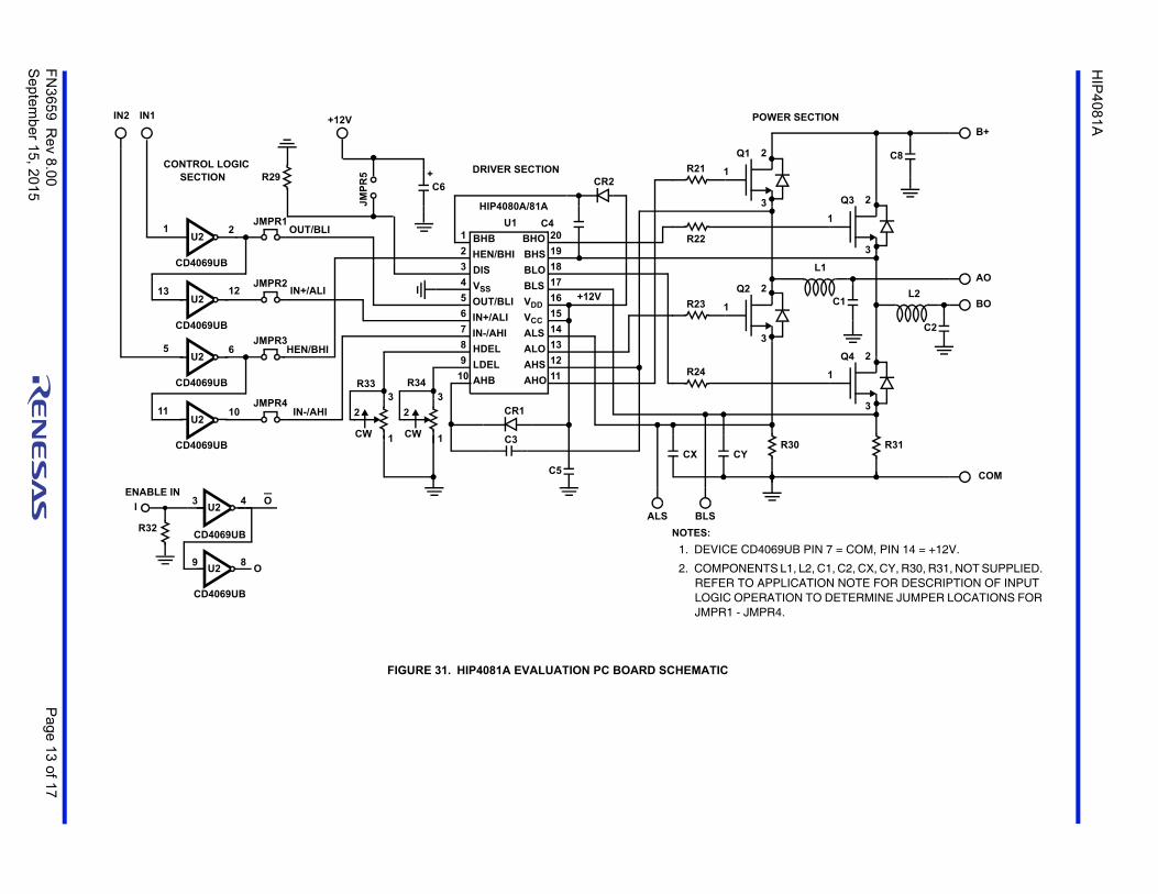
1. DEVICE CD4069UB PIN 7 = COM, PIN 14 = +12V.
2. COMPONENTS L1, L2, C1, C2, CX, CY, R30, R31, NOT SUPPLIED. REFER TO APPLICATION NOTE FOR DESCRIPTION OF INPUT LOGIC OPERATION TO DETERMINE JUMPER LOCATIONS FOR JMPR1 - JMPR4.
FIGURE 31. HIP4081A EVALUATION PC BOARD SCHEMATIC
FN
365
9R
ev 8
.00
Pa
ge 1
4 of 17
Se
ptemb
er 15, 20
15
HIP
408
1A
1
Q3
L1
C1
R3
1
1
Q4
L2
C2
BO
AO
COM
R22
JMPR2
JM
PR
5
R33
CR2
R23
R24
R27
R28
R26
1
Q2JMPR3
U1
R21
GND
C3
C4
JMPR4
JMPR1
R3
0
CR1
U2
R34
R3
2
I
O
C8R29
C7
C6
C5
CY
CX
1
Q1
+12VB+
IN1
IN2
AHO
BHO
ALO
BLOBLS
BLS
LDELH
DE
L
DIS
ALS
ALS
O
+ +
HIP
408
0/8
1
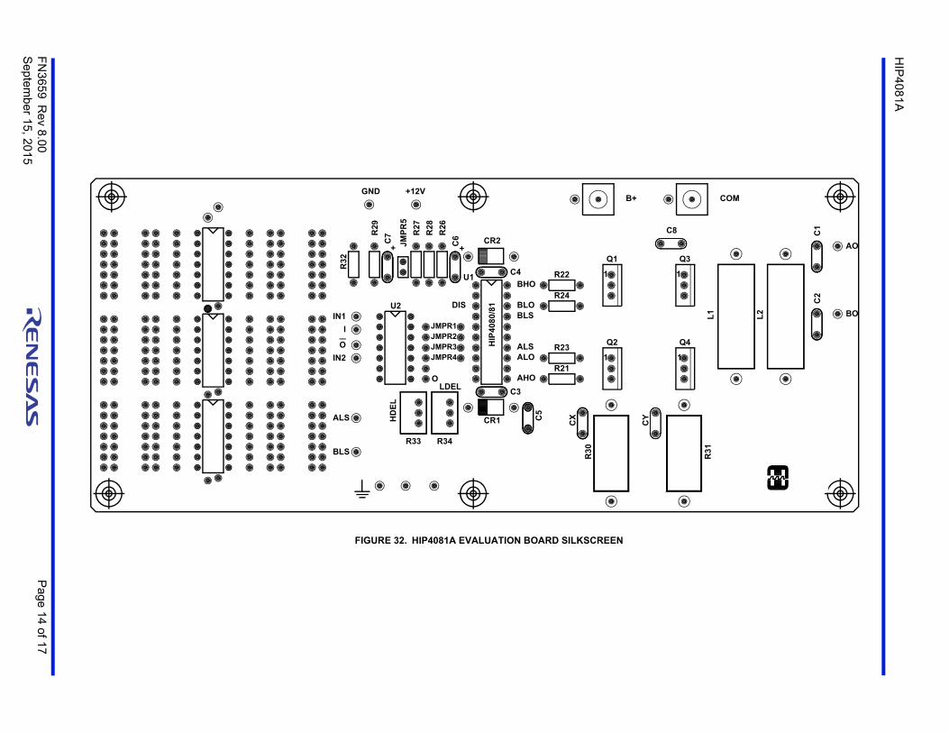
FIGURE 32. HIP4081A EVALUATION BOARD SILKSCREEN
HIP4081A
About IntersilIntersil Corporation is a leading provider of innovative power management and precision analog solutions. The company's products address some of the largest markets within the industrial and infrastructure, mobile computing and high-end consumer markets.
For the most updated datasheet, application notes, related documentation and related parts, please see the respective product information page found at www.intersil.com.
You may report errors or suggestions for improving this datasheet by visiting www.intersil.com/ask.
Reliability reports are also available from our website at www.intersil.com/support
Revision HistoryThe revision history provided is for informational purposes only and is believed to be accurate, but not warranted. Please go to the web to make sure that you have the latest revision.
DATE REVISION CHANGE
September 15, 2015 FN3659.8 Updated Ordering Information Table on page 1.Added Revision History and About Intersil sections.Updated POD M20.3 from rev 1 to rev 3. Changes since rev 1:
Top View:Corrected "7.50 BSC" to "7.60/7.40" (no change from rev 2; error was introduced in conversion)Changed "10.30 BSC" to "10.65/10.00" (no change from rev 2; error was introduced in conversion)Side View:Changed "12.80 BSC" to "13.00/12.60" (no change from rev 2; error was introduced in conversion)Changed "2.65 max" to "2.65/2.35" (no change from rev 2; error was introduced in conversion)
Changed Note 1 from "ANSI Y14.5M-1982." to "ASME Y14.5M-1994"
Updated to new POD format by moving dimensions from table onto drawing and adding land pattern
FN3659 Rev 8.00 Page 15 of 17September 15, 2015
FN3659 Rev 8.00 Page 16 of 17September 15, 2015
HIP4081A
Intersil products are manufactured, assembled and tested utilizing ISO9001 quality systems as notedin the quality certifications found at www.intersil.com/en/support/qualandreliability.html
Intersil products are sold by description only. Intersil may modify the circuit design and/or specifications of products at any time without notice, provided that such modification does not, in Intersil's sole judgment, affect the form, fit or function of the product. Accordingly, the reader is cautioned to verify that datasheets are current before placing orders. Information furnished by Intersil is believed to be accurate and reliable. However, no responsibility is assumed by Intersil or its subsidiaries for its use; nor for any infringements of patents or other rights of third parties which may result from its use. No license is granted by implication or otherwise under any patent or patent rights of Intersil or its subsidiaries.
For information regarding Intersil Corporation and its products, see www.intersil.com
For additional products, see www.intersil.com/en/products.html
© Copyright Intersil Americas LLC 2003-2015. All Rights Reserved.All trademarks and registered trademarks are the property of their respective owners.
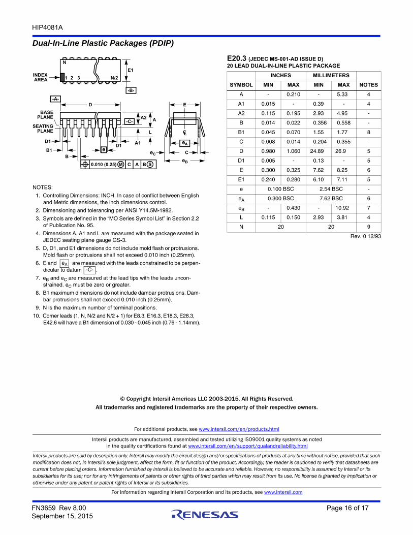
Dual-In-Line Plastic Packages (PDIP)
NOTES:
1. Controlling Dimensions: INCH. In case of conflict between English and Metric dimensions, the inch dimensions control.
2. Dimensioning and tolerancing per ANSI Y14.5M-1982.
3. Symbols are defined in the “MO Series Symbol List” in Section 2.2 of Publication No. 95.
4. Dimensions A, A1 and L are measured with the package seated in JEDEC seating plane gauge GS-3.
5. D, D1, and E1 dimensions do not include mold flash or protrusions. Mold flash or protrusions shall not exceed 0.010 inch (0.25mm).
6. E and are measured with the leads constrained to be perpen-dicular to datum .
7. eB and eC are measured at the lead tips with the leads uncon-strained. eC must be zero or greater.
8. B1 maximum dimensions do not include dambar protrusions. Dam-bar protrusions shall not exceed 0.010 inch (0.25mm).
9. N is the maximum number of terminal positions.
10. Corner leads (1, N, N/2 and N/2 + 1) for E8.3, E16.3, E18.3, E28.3, E42.6 will have a B1 dimension of 0.030 - 0.045 inch (0.76 - 1.14mm).
eA-C-
CL
E
eA
C
eB
eC
-B-
E1INDEX
1 2 3 N/2
N
AREA
SEATING
BASEPLANE
PLANE
-C-
D1
B1B
e
D
D1
AA2
L
A1
-A-
0.010 (0.25) C AM B S
E20.3 (JEDEC MS-001-AD ISSUE D)20 LEAD DUAL-IN-LINE PLASTIC PACKAGE
SYMBOL
INCHES MILLIMETERS
NOTESMIN MAX MIN MAX
A - 0.210 - 5.33 4
A1 0.015 - 0.39 - 4
A2 0.115 0.195 2.93 4.95 -
B 0.014 0.022 0.356 0.558 -
B1 0.045 0.070 1.55 1.77 8
C 0.008 0.014 0.204 0.355 -
D 0.980 1.060 24.89 26.9 5
D1 0.005 - 0.13 - 5
E 0.300 0.325 7.62 8.25 6
E1 0.240 0.280 6.10 7.11 5
e 0.100 BSC 2.54 BSC -
eA 0.300 BSC 7.62 BSC 6
eB - 0.430 - 10.92 7
L 0.115 0.150 2.93 3.81 4
N 20 20 9
Rev. 0 12/93
HIP4081A
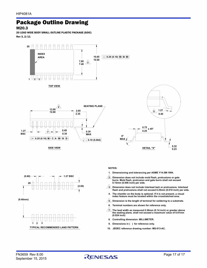
FN3659 Rev 8.00 Page 17 of 17September 15, 2015
Package Outline DrawingM20.320 LEAD WIDE BODY SMALL OUTLINE PLASTIC PACKAGE (SOIC)
Rev 3, 2/11
7. The lead width as measured 0.36mm (0.14 inch) or greater above the seating plane, shall not exceed a maximum value of 0.61mm
DETAIL "X"SIDE VIEW
TYPICAL RECOMMENDED LAND PATTERN
TOP VIEW
13.00
0.75
0.25x 45°
0.320.23
MAX8°
1.27
0.40
10.6510.00
7.607.40
20
1 2 3
INDEX
AREA
2.652.35
0.30MAXBSC
1.270.35
0.49
0.25 (0.10) M C SBMA0.10 (0.004)
0.25 (0.10) M B M
1 2
1.27 BSC
(9.40mm)
SEATING PLANE
(0.60)
(2.00)
2
20
3
3
5
7
NOTES:
1. Dimensioning and tolerancing per ASME Y14.5M-1994.
2. Dimension does not include mold flash, protrusions or gate
3. Dimension does not include interlead lash or protrusions. Interlead flash and protrusions shall not exceed 0.25mm (0.010 inch) per side.
4. The chamfer on the body is optional. If it is not present, a visual index feature must be located within the crosshatched area.
5. Dimension is the length of terminal for soldering to a substrate.
6. Terminal numbers are shown for reference only.
8. Controlling dimension: MILLIMETER.
9. Dimensions in ( ) for reference only.
burrs. Mold flash, protrusion and gate burrs shall not exceed 0.15mm (0.006 inch) per side.
(0.024 inch)
10. JEDEC reference drawing number: MS-013-AC.
12.60