Embed Size (px)
Citation preview
For price, delivery, and to place orders, please contact Hittite Microwave Corporation:20 Alpha Road, Chelmsford, MA 01824 Phone: 978-250-3343 Fax: 978-250-3373
Order On-line at www.hittite.com
MO
du
lAt
OR
s -
diR
eC
t q
uA
dR
Atu
Re
- s
Mt
10
10 - 1
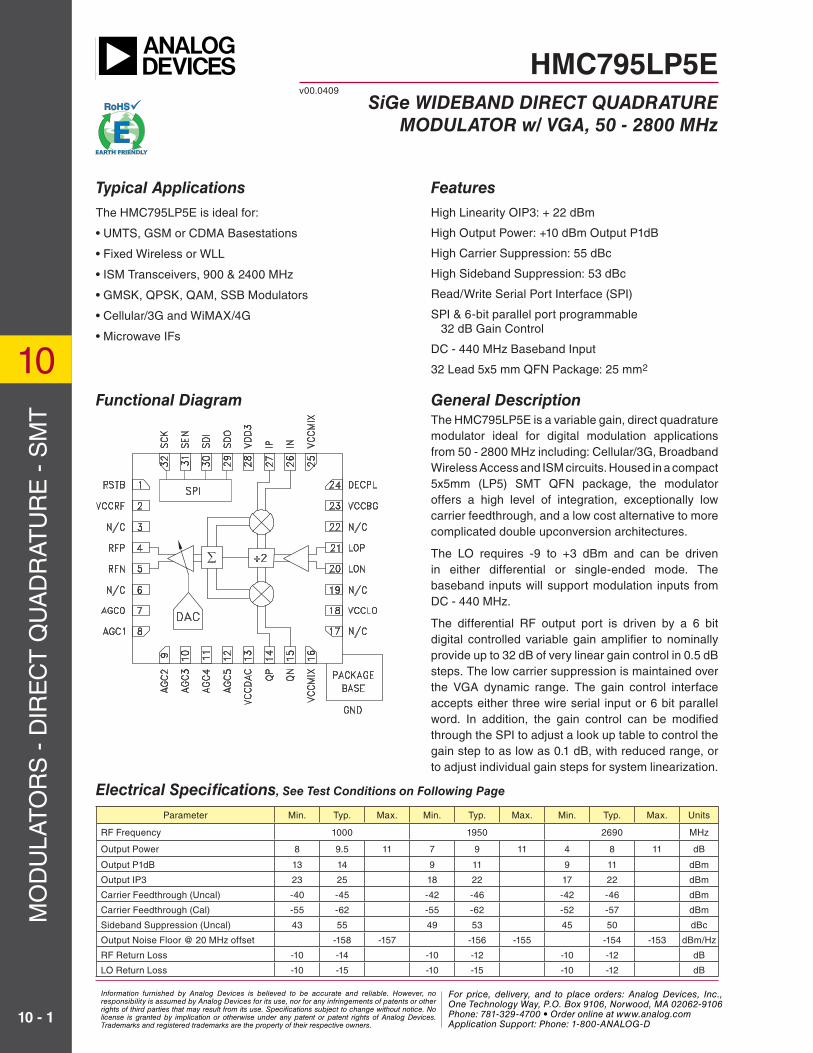
SiGe Wideband direct QuadratureModulator w/ vGa, 50 - 2800 MHz
v00.0409
HMC795LP5E
General description
Features
Functional diagram
typical applications
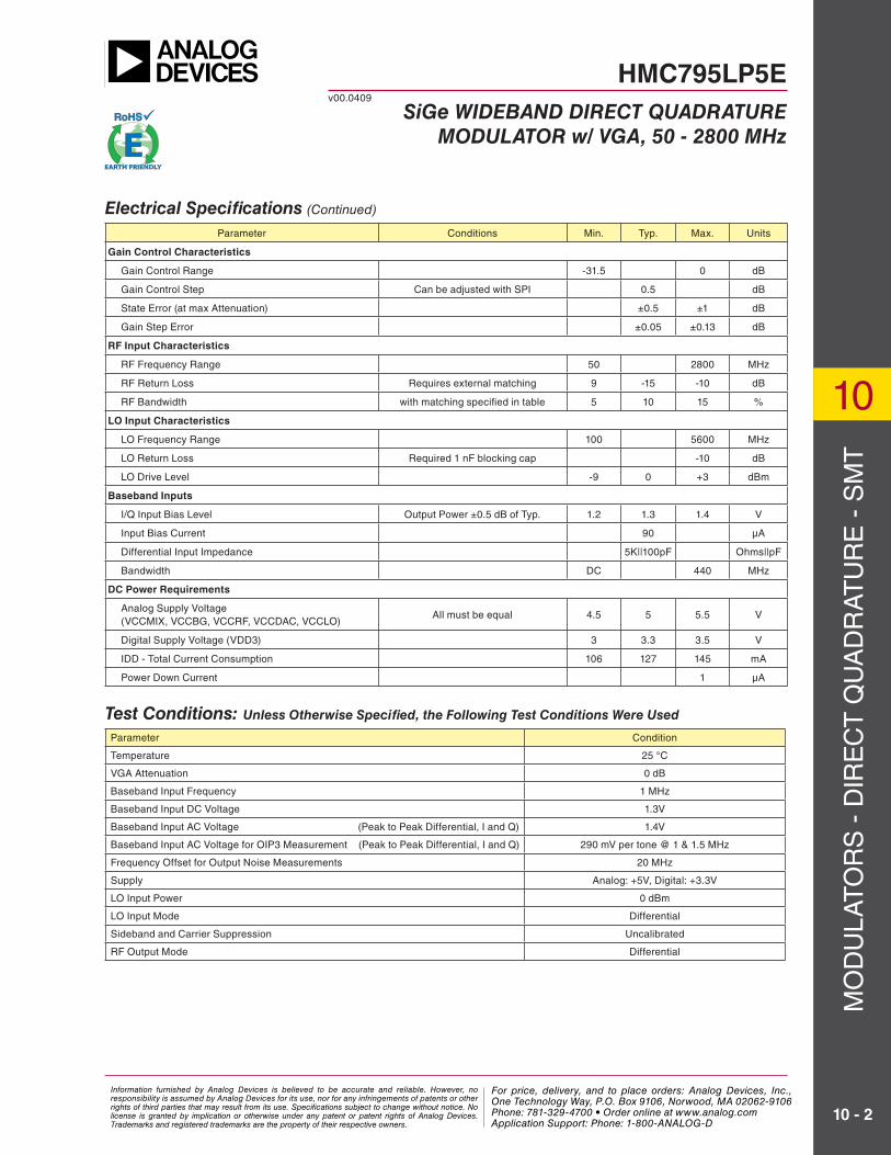
electrical Specifications, See test conditions on Following Page
the HMC795lP5e is a variable gain, direct quadrature modulator ideal for digital modulation applications from 50 - 2800 MHz including: Cellular/3G, Broadband Wireless Access and isM circuits. Housed in a compact 5x5mm (lP5) sMt qFN package, the modulator offers a high level of integration, exceptionally low carrier feedthrough, and a low cost alternative to more complicated double upconversion architectures.
the lO requires -9 to +3 dBm and can be driven in either differential or single-ended mode. the baseband inputs will support modulation inputs from dC - 440 MHz.
the differential RF output port is driven by a 6 bit digital controlled variable gain amplifier to nominally provide up to 32 dB of very linear gain control in 0.5 dB steps. the low carrier suppression is maintained over the VGA dynamic range. the gain control interface accepts either three wire serial input or 6 bit parallel word. in addition, the gain control can be modified through the sPi to adjust a look up table to control the gain step to as low as 0.1 dB, with reduced range, or to adjust individual gain steps for system linearization.
High linearity OiP3: + 22 dBm
High Output Power: +10 dBm Output P1dB
High Carrier suppression: 55 dBc
High sideband suppression: 53 dBc
Read/Write serial Port interface (sPi)
sPi & 6-bit parallel port programmable 32 dB Gain Control
dC - 440 MHz Baseband input
32 lead 5x5 mm qFN Package: 25 mm2
the HMC795lP5e is ideal for:
• uMts, GsM or CdMA Basestations
• Fixed Wireless or Wll
• isM transceivers, 900 & 2400 MHz
• GMsK, qPsK, qAM, ssB Modulators
• Cellular/3G and WiMAX/4G
• Microwave iFs
Parameter Min. typ. Max. Min. typ. Max. Min. typ. Max. units
RF Frequency 1000 1950 2690 MHz
Output Power 8 9.5 11 7 9 11 4 8 11 dB
Output P1dB 13 14 9 11 9 11 dBm
Output iP3 23 25 18 22 17 22 dBm
Carrier Feedthrough (uncal) -40 -45 -42 -46 -42 -46 dBm
Carrier Feedthrough (Cal) -55 -62 -55 -62 -52 -57 dBm
sideband suppression (uncal) 43 55 49 53 45 50 dBc
Output Noise Floor @ 20 MHz offset -158 -157 -156 -155 -154 -153 dBm/Hz
RF Return loss -10 -14 -10 -12 -10 -12 dB
lO Return loss -10 -15 -10 -15 -10 -12 dB
Information furnished by Analog Devices is believed to be accurate and reliable. However, no responsibility is assumed by Analog Devices for its use, nor for any infringements of patents or other rights of third parties that may result from its use. Specifications subject to change without notice. No license is granted by implication or otherwise under any patent or patent rights of Analog Devices. Trademarks and registered trademarks are the property of their respective owners.
For price, delivery, and to place orders: Analog Devices, Inc., One Technology Way, P.O. Box 9106, Norwood, MA 02062-9106 Phone: 781-329-4700 • Order online at www.analog.com Application Support: Phone: 1-800-ANALOG-D
For price, delivery, and to place orders, please contact Hittite Microwave Corporation:20 Alpha Road, Chelmsford, MA 01824 Phone: 978-250-3343 Fax: 978-250-3373
Order On-line at www.hittite.com
MO
du
lAt
OR
s -
diR
eC
t q
uA
dR
Atu
Re
- s
Mt
10
10 - 2
HMC795LP5Ev00.0409
SiGe Wideband direct QuadratureModulator w/ vGa, 50 - 2800 MHz
Parameter Conditions Min. typ. Max. units
Gain Control Characteristics
Gain Control Range -31.5 0 dB
Gain Control step Can be adjusted with sPi 0.5 dB
state error (at max Attenuation) ±0.5 ±1 dB
Gain step error ±0.05 ±0.13 dB
RF Input Characteristics
RF Frequency Range 50 2800 MHz
RF Return loss Requires external matching 9 -15 -10 dB
RF Bandwidth with matching specified in table 5 10 15 %
LO Input Characteristics
lO Frequency Range 100 5600 MHz
lO Return loss Required 1 nF blocking cap -10 dB
lO drive level -9 0 +3 dBm
Baseband Inputs
i/q input Bias level Output Power ±0.5 dB of typ. 1.2 1.3 1.4 V
input Bias Current 90 µA
differential input impedance 5K||100pF Ohms||pF
Bandwidth dC 440 MHz
DC Power Requirements
Analog supply Voltage (VCCMiX, VCCBG, VCCRF, VCCdAC, VCClO)
All must be equal 4.5 5 5.5 V
digital supply Voltage (Vdd3) 3 3.3 3.5 V
idd - total Current Consumption 106 127 145 mA
Power down Current 1 µA
electrical Specifications (Continued)
Parameter Condition
temperature 25 °C
VGA Attenuation 0 dB
Baseband input Frequency 1 MHz
Baseband input dC Voltage 1.3V
Baseband input AC Voltage (Peak to Peak differential, i and q) 1.4V
Baseband input AC Voltage for OiP3 Measurement (Peak to Peak differential, i and q) 290 mV per tone @ 1 & 1.5 MHz
Frequency Offset for Output Noise Measurements 20 MHz
supply Analog: +5V, digital: +3.3V
lO input Power 0 dBm
lO input Mode differential
sideband and Carrier suppression uncalibrated
RF Output Mode differential
test conditions: unless otherwise Specified, the Following test conditions Were used
Information furnished by Analog Devices is believed to be accurate and reliable. However, no responsibility is assumed by Analog Devices for its use, nor for any infringements of patents or other rights of third parties that may result from its use. Specifications subject to change without notice. No license is granted by implication or otherwise under any patent or patent rights of Analog Devices. Trademarks and registered trademarks are the property of their respective owners.
For price, delivery, and to place orders: Analog Devices, Inc., One Technology Way, P.O. Box 9106, Norwood, MA 02062-9106 Phone: 781-329-4700 • Order online at www.analog.com Application Support: Phone: 1-800-ANALOG-D

For price, delivery, and to place orders, please contact Hittite Microwave Corporation:20 Alpha Road, Chelmsford, MA 01824 Phone: 978-250-3343 Fax: 978-250-3373
Order On-line at www.hittite.com
MO
du
lAt
OR
s -
diR
eC
t q
uA
dR
Atu
Re
- s
Mt
10
10 - 3
HMC795LP5Ev00.0409
SiGe Wideband direct QuadratureModulator w/ vGa, 50 - 2800 MHz
calibrated vs. uncalibrated test resultsduring the uncalibrated Carrier suppression tests, care is taken to ensure that the i/q signal paths from the Vector signal Generator (VsG) to the device under test (dut) are equal. the “uncalibrated” Carrier suppression plots were measured at t= -40 °C, +25 °C, and +85 °C.
the “Calibrated” Carrier suppression data was plotted after a manual adjustment of the iP/iN & qP/qN dC offsets at +25 °C, 5V Vcc, 0 dBm lO input power level, and the RF output frequency set to the midband of the measurement range. the adjustment settings were held constant during tests over temperature and frequency.
output Power, output iP3 & Sideband Suppression vs. Freq. over temperature [1]
typical Performance characteristics, vcc +5v, lo 0 dbm, +25 °c
output Power & output noise @ 1 GHz vs. vGa attenuation over temperature [1]
uncalibrated & calibrated carrier Feedthrough vs. Freq. over temperature [1]
carrier Feedthrough & Sideband Suppression @ 1 GHz vs. vGa attenuation over temperature [1]
-20
-10
0
10
20
30
40
-60
-50
-40
-30
-20
-10
0
800 850 900 950 1000 1050 1100 1150 1200
+25 C+85 C -40 C
FREQUENCY (MHz)
OU
TP
UT
PO
WE
R (
dBm
), O
UT
PU
T IP
3 (d
Bm
)
SID
EB
AN
D S
UP
PR
ES
SIO
N (dB
c)
OUTPUT POWER
SIDEBAND SUPPRESSION
OUTPUT IP3
-80
-75
-70
-65
-60
-55
-50
-45
-40
800 850 900 950 1000 1050 1100 1150 1200
+25 C+85 C -40 C
FREQUENCY (MHz)
CA
RR
IER
FE
ED
TH
RO
UG
H (
dBm
)
UNCALIBRATED
CALIBRATED
-40
-30
-20
-10
0
10
20
-180
-170
-160
-150
-140
-130
-120
0 4 8 12 16 20 24 28 32
+25 C+85 C -40 C
ATTENUATION (dB)
OU
TP
UT
PO
WE
R (
dBm
)
OU
TP
UT
NO
ISE
@ 20 M
Hz (dB
m/H
z)
OUTPUT POWER
OUTPUT NOISE
-90
-85
-80
-75
-70
-65
-60
-55
-50
-60
-55
-50
-45
-40
0 4 8 12 16 20 24 28 32
+25 C+85 C -40 C
ATTENUATION (dB)
CA
RR
IER
FE
ED
TH
RO
UG
H (
dBm
) SID
EB
AN
D S
UP
PR
ES
SIO
N (dB
c)
CARRIER FEEDTHROUGH
SIDEBAND SUPPRESSION
[1] Output Matched to 1 GHz
Information furnished by Analog Devices is believed to be accurate and reliable. However, no responsibility is assumed by Analog Devices for its use, nor for any infringements of patents or other rights of third parties that may result from its use. Specifications subject to change without notice. No license is granted by implication or otherwise under any patent or patent rights of Analog Devices. Trademarks and registered trademarks are the property of their respective owners.
For price, delivery, and to place orders: Analog Devices, Inc., One Technology Way, P.O. Box 9106, Norwood, MA 02062-9106 Phone: 781-329-4700 • Order online at www.analog.com Application Support: Phone: 1-800-ANALOG-D

For price, delivery, and to place orders, please contact Hittite Microwave Corporation:20 Alpha Road, Chelmsford, MA 01824 Phone: 978-250-3343 Fax: 978-250-3373
Order On-line at www.hittite.com
MO
du
lAt
OR
s -
diR
eC
t q
uA
dR
Atu
Re
- s
Mt
10
10 - 4
HMC795LP5Ev00.0409
SiGe Wideband direct QuadratureModulator w/ vGa, 50 - 2800 MHz
output Power & output noise @ 1 GHz vs. input baseband amplitude over temperature [1]
output Power, output iP3 & Sideband Suppression vs. Freq. over lo Power [1]
output Power, output iP3 & Sideband Sup-pression vs. Freq. over Supply voltage [1]
carrier Feedthrough & Sideband Suppression @ 1 GHz vs. input baseband amplitude over temperature [1]
uncalibrated & calibrated carrier Feedthrough vs. Freq. over lo Power [1]
uncalibrated & calibrated carrier Feed-through vs. Freq. over Supply voltage [1]
-10
-5
0
5
10
15
20
-160
-155
-150
-145
+25 C+85 C -40 C
0.1 1
OU
TP
UT
NO
ISE
@ 20 M
Hz (dB
m/H
z)
INPUT BASEBAND AMPLITUDE (Vp-p diff)
OUTPUT POWER
OUTPUT NOISE
OU
TP
UT
PO
WE
R (
dBm
)
OP1dB 14.1 dBmOP1dB 14.3 dBm
OP1dB 14.0 dBm
2 3
-20
-10
0
10
20
30
40
-60
-50
-40
-30
-20
-10
0
800 850 900 950 1000 1050 1100 1150 1200
0 dBm+3 dBm -9 dBm
FREQUENCY (MHz)
OU
TP
UT
PO
WE
R (
dBm
), O
UT
PU
T IP
3 (d
Bm
)
SID
EB
AN
D S
UP
PR
ES
SIO
N (dB
c)
OUTPUT POWER
SIDEBAND SUPPRESSION
OUTPUT IP3
-20
-10
0
10
20
30
40
-60
-50
-40
-30
-20
-10
0
800 850 900 950 1000 1050 1100 1150 1200
4.5V5.0V5.5V
FREQUENCY (MHz)
OU
TP
UT
PO
WE
R (
dBm
), O
UT
PU
T IP
3 (d
Bm
)
SID
EB
AN
D S
UP
PR
ES
SIO
N (dB
c)
OUTPUT POWER
SIDEBAND SUPPRESSION
OUTPUT IP3
-70
-65
-60
-55
-50
-45
-40
-70
-65
-60
-55
-50
-45
-40
0.1 1
+25 C+85 C -40 C
INPUT BASEBAND AMPLITUDE (Vp-p diff)
CA
RR
IER
FE
ED
TH
RO
UG
H (
dBm
)
SID
EB
AN
D S
UP
PR
ES
SIO
N (dB
c)
CARRIER FEEDTHROUGH
SIDEBAND SUPPRESSION
2 3
-80
-75
-70
-65
-60
-55
-50
-45
-40
800 850 900 950 1000 1050 1100 1150 1200
0 dBm+3 dBm -9 dBm
FREQUENCY (MHz)
CA
RR
IER
FE
ED
TH
RO
UG
H (
dBm
) UNCALIBRATED
CALIBRATED
-80
-75
-70
-65
-60
-55
-50
-45
-40
800 850 900 950 1000 1050 1100 1150 1200
4.5 V5.0 V5.5 V
FREQUENCY (MHz)
CA
RR
IER
FE
ED
TH
RO
UG
H (
dBm
) UNCALIBRATED
CALIBRATED
[1] Output Matched to 1 GHz
Information furnished by Analog Devices is believed to be accurate and reliable. However, no responsibility is assumed by Analog Devices for its use, nor for any infringements of patents or other rights of third parties that may result from its use. Specifications subject to change without notice. No license is granted by implication or otherwise under any patent or patent rights of Analog Devices. Trademarks and registered trademarks are the property of their respective owners.
For price, delivery, and to place orders: Analog Devices, Inc., One Technology Way, P.O. Box 9106, Norwood, MA 02062-9106 Phone: 781-329-4700 • Order online at www.analog.com Application Support: Phone: 1-800-ANALOG-D

For price, delivery, and to place orders, please contact Hittite Microwave Corporation:20 Alpha Road, Chelmsford, MA 01824 Phone: 978-250-3343 Fax: 978-250-3373
Order On-line at www.hittite.com
MO
du
lAt
OR
s -
diR
eC
t q
uA
dR
Atu
Re
- s
Mt
10
10 - 5
HMC795LP5Ev00.0409
SiGe Wideband direct QuadratureModulator w/ vGa, 50 - 2800 MHz
output Power, output iP3 & Sideband Suppression vs. Freq. over temperature [1]
uncalibrated & calibrated carrier Feedthrough vs. Freq. over temperature [1]
[1] Output Matched to 1950 MHz
output Power & output noise @ 1950 MHz vs. vGa attenuation MHz over temperature [1]
carrier Feedthrough & Sideband Suppression @ 1950 MHz vs. vGa attenuation over temperature [1]
-20
-10
0
10
20
30
40
-60
-50
-40
-30
-20
-10
0
1800 1850 1900 1950 2000 2050 2100 2150 2200
+25 C+85 C -40 C
FREQUENCY (MHz)
OU
TP
UT
PO
WE
R (
dBm
), O
UT
PU
T IP
3 (d
Bm
)
SID
EB
AN
D S
UP
PR
ES
SIO
N (dB
c)
OUTPUT POWER
SIDEBAND SUPPRESSION
OUTPUT IP3
-40
-30
-20
-10
0
10
20
-180
-170
-160
-150
-140
-130
-120
0 4 8 12 16 20 24 28 32
+25 C+85 C -40 C
ATTENUATION (dB)
OU
TP
UT
PO
WE
R (
dBm
)
OU
TP
UT
NO
ISE
@20M
Hz (dB
m/H
z)
OUTPUT POWER
OUTPUT NOISE
-20
-15
-10
-5
0
5
10
15
20
-160
-155
-150
-145
-140
0.1 1
+25 C+85 C -40 C
OU
TP
UT
NO
ISE
@ 20 M
Hz (dB
m/H
z)
INPUT BASEBAND AMPLITUDE (Vp-p diff)
OUTPUT POWER
OUTPUT NOISE
OU
TP
UT
PO
WE
R (
dBm
)
OP1dB 11.6 dBmOP1dB 10.9 dBm
OP1dB 11.8 dBm
2 3
-80
-75
-70
-65
-60
-55
-50
-45
-40
1800 1850 1900 1950 2000 2050 2100 2150 2200
+25 C+85 C -40 C
FREQUENCY (MHz)
CA
RR
IER
FE
ED
TH
RO
UG
H (
dBm
)
UNCALIBRATED
CALIBRATED
-90
-85
-80
-75
-70
-65
-60
-55
-50
-60
-55
-50
-45
-40
0 4 8 12 16 20 24 28 32
+25 C+85 C -40 C
ATTENUATION (dB)
CA
RR
IER
FE
ED
TH
RO
UG
H (
dBm
) SID
EB
AN
D S
UP
PR
ES
SIO
N (dB
c)
CARRIER FEEDTHROUGH
SIDEBAND SUPPRESSION
-70
-65
-60
-55
-50
-45
-40
-60
-55
-50
-45
-40
-35
-30
0.1 1
+25 C+85 C -40 C
INPUT BASEBAND AMPLITUDE (Vp-p diff)
CA
RR
IER
FE
ED
TH
RO
UG
H (
dBm
)
SID
EB
AN
D S
UP
PR
ES
SIO
N (dB
c)
CARRIER FEEDTHROUGH
SIDEBAND SUPPRESSION
2 3
output Power & output noise @ 1950 MHz vs. input baseband amplitude over temperature [1]
carrier Feedthrough & Sideband Suppression @ 1950 MHz vs. input baseband amplitude over temperature [1]
Information furnished by Analog Devices is believed to be accurate and reliable. However, no responsibility is assumed by Analog Devices for its use, nor for any infringements of patents or other rights of third parties that may result from its use. Specifications subject to change without notice. No license is granted by implication or otherwise under any patent or patent rights of Analog Devices. Trademarks and registered trademarks are the property of their respective owners.
For price, delivery, and to place orders: Analog Devices, Inc., One Technology Way, P.O. Box 9106, Norwood, MA 02062-9106 Phone: 781-329-4700 • Order online at www.analog.com Application Support: Phone: 1-800-ANALOG-D

For price, delivery, and to place orders, please contact Hittite Microwave Corporation:20 Alpha Road, Chelmsford, MA 01824 Phone: 978-250-3343 Fax: 978-250-3373
Order On-line at www.hittite.com
MO
du
lAt
OR
s -
diR
eC
t q
uA
dR
Atu
Re
- s
Mt
10
10 - 6
HMC795LP5Ev00.0409
SiGe Wideband direct QuadratureModulator w/ vGa, 50 - 2800 MHz
[1] Output Matched to 1950 MHz [2] Output Matched to 2690 MHz
output Power, output iP3 & Sideband Suppression vs. Freq. over lo Power [1]
output Power, output iP3 & Sideband Sup-pression vs. Freq. over Supply voltage [1]
uncalibrated & calibrated carrier Feedthrough vs. Freq. over lo Power [1]
uncalibrated & calibrated carrier Feed-through vs. Freq. over Supply voltage [1]
output Power, output iP3 & Sideband Suppression vs. Freq. over temperature [2]
uncalibrated & calibrated carrier Feedthrough vs. Freq. over temperature [2]
-20
-10
0
10
20
30
40
-60
-50
-40
-30
-20
-10
0
1800 1850 1900 1950 2000 2050 2100 2150 2200
0 dBm+3 dBm -9 dBm
FREQUENCY (MHz)
OU
TP
UT
PO
WE
R (
dBm
), O
UT
PU
T IP
3 (d
Bm
)
SID
EB
AN
D S
UP
PR
ES
SIO
N (dB
c)
OUTPUT POWER
SIDEBAND SUPPRESSION
OUTPUT IP3
-20
-10
0
10
20
30
40
-60
-50
-40
-30
-20
-10
0
1800 1850 1900 1950 2000 2050 2100 2150 2200
4.5V5.0V5.5V
FREQUENCY (MHz)
OU
TP
UT
PO
WE
R (
dBm
), O
UT
PU
T IP
3 (d
Bm
)
SID
EB
AN
D S
UP
PR
ES
SIO
N (dB
c)
OUTPUT POWER
SIDEBAND SUPPRESSION
OUTPUT IP3
-40
-30
-20
-10
0
10
20
30
40
-70
-60
-50
-40
-30
-20
-10
0
10
2500 2550 2600 2650 2700 2750 2800
+25 C+85 C -40 C
FREQUENCY (MHz)
PO
WE
R (
dBm
) &
IP3
(dB
m)
SID
EB
AN
D S
UP
PR
ES
SIO
N (dB
c)
OUTPUT POWER
SIDEBAND SUPPRESSION
OUTPUT IP3
-80
-75
-70
-65
-60
-55
-50
-45
-40
1800 1850 1900 1950 2000 2050 2100 2150 2200
0 dBm+3 dBm -9 dBm
FREQUENCY (MHz)
CA
RR
IER
FE
ED
TH
RO
UG
H (
dBm
)
UNCALIBRATED
CALIBRATED
-80
-75
-70
-65
-60
-55
-50
-45
-40
1800 1850 1900 1950 2000 2050 2100 2150 2200
4.5 V5.0 V5.5 V
FREQUENCY (MHz)
CA
RR
IER
FE
ED
TH
RO
UG
H (
dBm
)
UNCALIBRATED
CALIBRATED
-60
-55
-50
-45
-40
-35
-30
2500 2550 2600 2650 2700 2750 2800
+25 C+85 C -40 C
FREQUENCY (MHz)
CA
RR
IER
FE
ED
TH
RO
UG
H (
dBm
) UNCALIBRATED
CALIBRATED
Information furnished by Analog Devices is believed to be accurate and reliable. However, no responsibility is assumed by Analog Devices for its use, nor for any infringements of patents or other rights of third parties that may result from its use. Specifications subject to change without notice. No license is granted by implication or otherwise under any patent or patent rights of Analog Devices. Trademarks and registered trademarks are the property of their respective owners.
For price, delivery, and to place orders: Analog Devices, Inc., One Technology Way, P.O. Box 9106, Norwood, MA 02062-9106 Phone: 781-329-4700 • Order online at www.analog.com Application Support: Phone: 1-800-ANALOG-D

For price, delivery, and to place orders, please contact Hittite Microwave Corporation:20 Alpha Road, Chelmsford, MA 01824 Phone: 978-250-3343 Fax: 978-250-3373
Order On-line at www.hittite.com
MO
du
lAt
OR
s -
diR
eC
t q
uA
dR
Atu
Re
- s
Mt
10
10 - 7
[1] Output Matched to 2960 MHz
output Power & output noise @ 2690 MHz vs. vGa attenuation over temperature [1]
carrier Feedthrough & Sideband Suppression @ 2960 MHz vs. vGa attenuation over temperature [1]
output Power & output noise @ 2960 MHz vs. input baseband amplitude over temperature [1]
carrier Feedthrough & Sideband Suppression @ 2960 MHz vs. input base-band amplitude over temperature [1]
output Power, output iP3 & Sideband Suppression vs. Freq. over lo Power [1]
uncalibrated & calibrated carrier Feedthrough vs. Freq. over lo Power [1]
HMC795LP5Ev00.0409
SiGe Wideband direct QuadratureModulator w/ vGa, 50 - 2800 MHz
-40
-30
-20
-10
0
10
20
-180
-170
-160
-150
-140
-130
-120
0 4 8 12 16 20 24 28 32
+25C+85C -40C
OU
TP
UT
NO
ISE
@ 20 M
Hz (dB
m/H
z)ATTENUATION (dB)
OUTPUT POWER
OUTPUT NOISE
OU
TP
UT
PO
WE
R (
dBm
)
-20
-10
0
10
20
-155
-150
-145
-140
-135
0.1 1
+25 C+85 C -40 C
OU
TP
UT
NO
ISE
@ 20 M
Hz (dB
m/H
z)
INPUT BASEBAND AMPLITUDE (Vp-p diff)
OUTPUT POWER
OUTPUT NOISE
OU
TP
UT
PO
WE
R (
dBm
)
OP1dB 11.9 dBm
OP1dB 12.3 dBm
OP1dB 11.1 dBm
2 3
-20
-10
0
10
20
30
40
-60
-50
-40
-30
-20
-10
0
2500 2550 2600 2650 2700 2750 2800
0 dBm+3 dBm -9 dBm
FREQUENCY (MHz)
OU
TP
UT
PO
WE
R (
dBm
), O
UT
PU
T IP
3 (d
Bm
)
SID
EB
AN
D S
UP
PR
ES
SIO
N (dB
c)
OUTPUT POWER
SIDEBAND SUPPRESSION
OUTPUT IP3
-80
-70
-60
-50
-40
-30
-20
-10
-100
-90
-80
-70
-60
-50
-40
-30
0 4 8 12 16 20 24 28 32
+25 C+85 C -40 C
ATTENUATION (dB)
CA
RR
IER
FE
ED
TH
RO
UG
H (
dBm
)
SID
EB
AN
D S
UP
PR
ES
SIO
N (dB
c)
CARRIER FEEDTHROUGH
SIDEBAND SUPPRESSION
-70
-60
-50
-40
-30
-60
-50
-40
-30
-20
0.1 1
+25 C+85 C -40 C
INPUT BASEBAND AMPLITUDE (Vp-p diff)
CA
RR
IER
FE
ED
TH
RO
UG
H (
dBm
)
SID
EB
AN
D S
UP
PR
ES
SIO
N (dB
c)
CARRIER FEEDTHROUGH
SIDEBAND SUPPRESSION
2 3
-60
-55
-50
-45
-40
-35
-30
2500 2550 2600 2650 2700 2750 2800
0 dBm+3 dBm -9 dBm
FREQUENCY (MHz)
CA
RR
IER
FE
ED
TH
RO
UG
H (
dBm
)
UNCALIBRATED
CALIBRATED
Information furnished by Analog Devices is believed to be accurate and reliable. However, no responsibility is assumed by Analog Devices for its use, nor for any infringements of patents or other rights of third parties that may result from its use. Specifications subject to change without notice. No license is granted by implication or otherwise under any patent or patent rights of Analog Devices. Trademarks and registered trademarks are the property of their respective owners.
For price, delivery, and to place orders: Analog Devices, Inc., One Technology Way, P.O. Box 9106, Norwood, MA 02062-9106 Phone: 781-329-4700 • Order online at www.analog.com Application Support: Phone: 1-800-ANALOG-D

For price, delivery, and to place orders, please contact Hittite Microwave Corporation:20 Alpha Road, Chelmsford, MA 01824 Phone: 978-250-3343 Fax: 978-250-3373
Order On-line at www.hittite.com
MO
du
lAt
OR
s -
diR
eC
t q
uA
dR
Atu
Re
- s
Mt
10
10 - 8
output Power, output iP3 & Sideband Sup-pression vs. Freq. over Supply voltage [1]
normalized attenuation vs. Frequency (only Major States are Shown)
absolute error [2] vs. attenuation State
uncalibrated & calibrated carrier Feed-through vs. Freq. over Supply voltage [1]
absolute error [2] vs. Frequency(Only Major States are Shown)
Step error [3] vs. Frequency(Only Major States are Shown)
[1] Output Matched to 2960 MHz[2] Absolute error - difference between measured and ideal attenuation[3] step error - difference between measured attuation step and ideal step of 0.5 dB
HMC795LP5Ev00.0409
SiGe Wideband direct QuadratureModulator w/ vGa, 50 - 2800 MHz
-20
-10
0
10
20
30
40
-60
-50
-40
-30
-20
-10
0
2500 2550 2600 2650 2700 2750 2800
4.5V5.0V5.5V
FREQUENCY (MHz)
PO
WE
R (
dBm
) &
IP3
(dB
m)
SID
EB
AN
D S
UP
PR
ES
SIO
N (dB
c)
OUTPUT POWER
SIDEBAND SUPPRESSION
OUTPUT IP3
-35
-30
-25
-20
-15
-10
-5
0
0 0.5 1 1.5 2 2.5
FREQUENCY (GHz)
NO
RM
ALI
ZE
D A
TT
EN
UA
TIO
N (
dB)
-0.5
-0.25
0
0.25
0.5
0 4 8 12 16 20 24 28 32
ATTENUATION (dB)
AB
SO
LUT
E E
RR
OR
(dB
)
50 MHz1 GHz
2 GHz2.5 GHz
-60
-55
-50
-45
-40
-35
-30
2500 2550 2600 2650 2700 2750 2800
4.5 V5.0 V5.5 V
FREQUENCY (MHz)
CA
RR
IER
FE
ED
TH
RO
UG
H (
dBm
)
UNCALIBRATED
CALIBRATED
-1
-0.5
0
0.5
1
0 0.5 1 1.5 2 2.5
FREQUENCY (GHz)
AB
SO
LUT
E E
RR
OR
(dB
)
-0.5
-0.25
0
0.25
0.5
0 0.5 1 1.5 2 2.5
FREQUENCY (GHz)
ST
EP
ER
RO
R (
dB)
Information furnished by Analog Devices is believed to be accurate and reliable. However, no responsibility is assumed by Analog Devices for its use, nor for any infringements of patents or other rights of third parties that may result from its use. Specifications subject to change without notice. No license is granted by implication or otherwise under any patent or patent rights of Analog Devices. Trademarks and registered trademarks are the property of their respective owners.
For price, delivery, and to place orders: Analog Devices, Inc., One Technology Way, P.O. Box 9106, Norwood, MA 02062-9106 Phone: 781-329-4700 • Order online at www.analog.com Application Support: Phone: 1-800-ANALOG-D

For price, delivery, and to place orders, please contact Hittite Microwave Corporation:20 Alpha Road, Chelmsford, MA 01824 Phone: 978-250-3343 Fax: 978-250-3373
Order On-line at www.hittite.com
MO
du
lAt
OR
s -
diR
eC
t q
uA
dR
Atu
Re
- s
Mt
10
10 - 9
Step error vs. attenuation
lo return loss vs. Frequency
acPr for W-cdMa @ 2140 MHz vs. output Power for various input levels, vGa attenuation 0 db [1]
acPr for W-cdMa @ 2140 MHz vs. output Power & vGa attenuation for various input levels [1]
rF return loss vs. attenuation
rF return loss vs. Frequency offset, vGa attenuation 0 db
HMC795LP5Ev00.0409
SiGe Wideband direct QuadratureModulator w/ vGa, 50 - 2800 MHz
-0.15
-0.1
-0.05
0
0.05
0.1
0.15
0 4 8 12 16 20 24 28 32
ATTENUATION (dB)
ST
EP
ER
RO
R (
dB)
50 MHz, 1 GHz, 2 GHz, 2.5 GHz
-40
-30
-20
-10
0
0 1 2 3 4 5
FREQUENCY (GHz)
RE
TU
RN
LO
SS
(dB
)
SINGLE-ENDED LO
DIFFERENTIAL LOWITH BD2326 BALUN
-75
-70
-65
-60
-55
-50
-15 -10 -5 0
CARRIER OUTPUT POWER (dBm)
AC
PR
(dB
c)
ADJACENT CH. ACPR
ALTERNATE CH. ACPR
-30
-25
-20
-15
-10
-5
0
0 4 8 12 16 20 24 28 32
ATTENUATION STATE (dB)
RF
RE
TU
RN
LO
SS
(dB
)
1000MHz
2690MHz
1950 MHz
-30
-25
-20
-15
-10
-5
0
-150 -100 -50 0 50 100 150
OFFSET FREQUENCY (MHz)
1000MHz
RE
TU
RN
LO
SS
(dB
)
1950MHz
2690MHz
-90
-80
-70
-60
-50
-40
-30
-180
-160
-140
-120
-100
-80
-60
-40 -30 -20 -10 0 10
OU
TP
UT
NO
ISE
@ 20 M
Hz (dB
m/H
z)
CARRIER OUTPUT POWER (dBm)
ACPR
OUTPUT NOISE
AC
PR
(dB
)
110mV (rms)
65mV (rms)
0 dB
0 dB
0 dB
31.5dB
31.5dB
0 dB
28dB
37mV (rms)
[1] W-CdMA (Modulation set-up for ACPR Mode): the baseband i and q input signals were generated using “test Model 1 with 64 channels
Information furnished by Analog Devices is believed to be accurate and reliable. However, no responsibility is assumed by Analog Devices for its use, nor for any infringements of patents or other rights of third parties that may result from its use. Specifications subject to change without notice. No license is granted by implication or otherwise under any patent or patent rights of Analog Devices. Trademarks and registered trademarks are the property of their respective owners.
For price, delivery, and to place orders: Analog Devices, Inc., One Technology Way, P.O. Box 9106, Norwood, MA 02062-9106 Phone: 781-329-4700 • Order online at www.analog.com Application Support: Phone: 1-800-ANALOG-D

For price, delivery, and to place orders, please contact Hittite Microwave Corporation:20 Alpha Road, Chelmsford, MA 01824 Phone: 978-250-3343 Fax: 978-250-3373
Order On-line at www.hittite.com
MO
du
lAt
OR
s -
diR
eC
t q
uA
dR
Atu
Re
- s
Mt
10
10 - 10
absolute Maximum ratings truth tableVCCMiX, VCCBG, VCCRF, VCCdAC -0.3V to +5.5V
Vdd3 -0.3V to +3.6V
lO input Power +18 dBm
Baseband input Voltage (dC) 0V to +1.4V
Baseband input Voltage (AC + dC) 0V to +1.8V
Maximum Junction temperature 125 °C
Continuous Pdiss (t = 85°C)(derate 25 mW/°C above 85°C)
1W
thermal Resistance (Rth)(junction to ground paddle)
40 °C/W
storage temperature -65 to +150 °C
Operating temperature -40 to +85 °C
Reflow solderingPeak temperature 260 °C
esd sensitivity (HBM) Class 1B
Control Voltage inputAttenuation
AGC5 AGC4 AGC3 AGC2 AGC1 AGC1
low low low low low low 0 dB
low low low low low High 0.5 dB
low low low low High low 1 dB
low low low High low low 2 dB
low low High low low low 4 dB
low High low low low low 8 dB
High low low low low low 16 dB
High High High High High High 31.5 dB
Any combination of the above states will provide an increase in the attenuation approximately equal to the sum of the bits selected
eleCtROstAtiC seNsitiVe deViCeOBseRVe HANdliNG PReCAutiONs
stresses above those listed under Absolute Maximum Ratings may cause permanent damage to the device. this is a stress rating only; functional operation of the device at these or any other conditions above those indicated in the operational section of this specification is not implied. exposure to absolute maximum rating conditions for extended periods may affect device reliability.
outline drawing
NOtes:
1. leAdFRAMe MAteRiAl: COPPeR AllOY
2. diMeNsiONs ARe iN iNCHes [MilliMeteRs]
3. leAd sPACiNG tOleRANCe is NON-CuMulAtiVe.
4. PAd BuRR leNGtH sHAll Be 0.15mm MAXiMuM.
PAd BuRR HeiGHt sHAll Be 0.05mm MAXiMuM.
5. PACKAGe WARP sHAll NOt eXCeed 0.05mm.
6. All GROuNd leAds ANd GROuNd PAddle Must Be sOldeRed tO PCB RF GROuNd.
7. ReFeR tO Hittite APPliCAtiON NOte FOR suGGested lANd PAtteRN.
Part Number Package Body Material lead Finish Msl Rating Package Marking [1]
HMC795lP5e RoHs-compliant low stress injection Molded Plastic 100% matte sn Msl1 [2] H795XXXX
[1] 4-digit lot number XXXX[2] Max peak reflow temperature of 260 °C
Package information
HMC795LP5Ev00.0409
SiGe Wideband direct QuadratureModulator w/ vGa, 50 - 2800 MHz
Information furnished by Analog Devices is believed to be accurate and reliable. However, no responsibility is assumed by Analog Devices for its use, nor for any infringements of patents or other rights of third parties that may result from its use. Specifications subject to change without notice. No license is granted by implication or otherwise under any patent or patent rights of Analog Devices. Trademarks and registered trademarks are the property of their respective owners.
For price, delivery, and to place orders: Analog Devices, Inc., One Technology Way, P.O. Box 9106, Norwood, MA 02062-9106 Phone: 781-329-4700 • Order online at www.analog.com Application Support: Phone: 1-800-ANALOG-D
For price, delivery, and to place orders, please contact Hittite Microwave Corporation:20 Alpha Road, Chelmsford, MA 01824 Phone: 978-250-3343 Fax: 978-250-3373
Order On-line at www.hittite.com
MO
du
lAt
OR
s -
diR
eC
t q
uA
dR
Atu
Re
- s
Mt
10
10 - 11
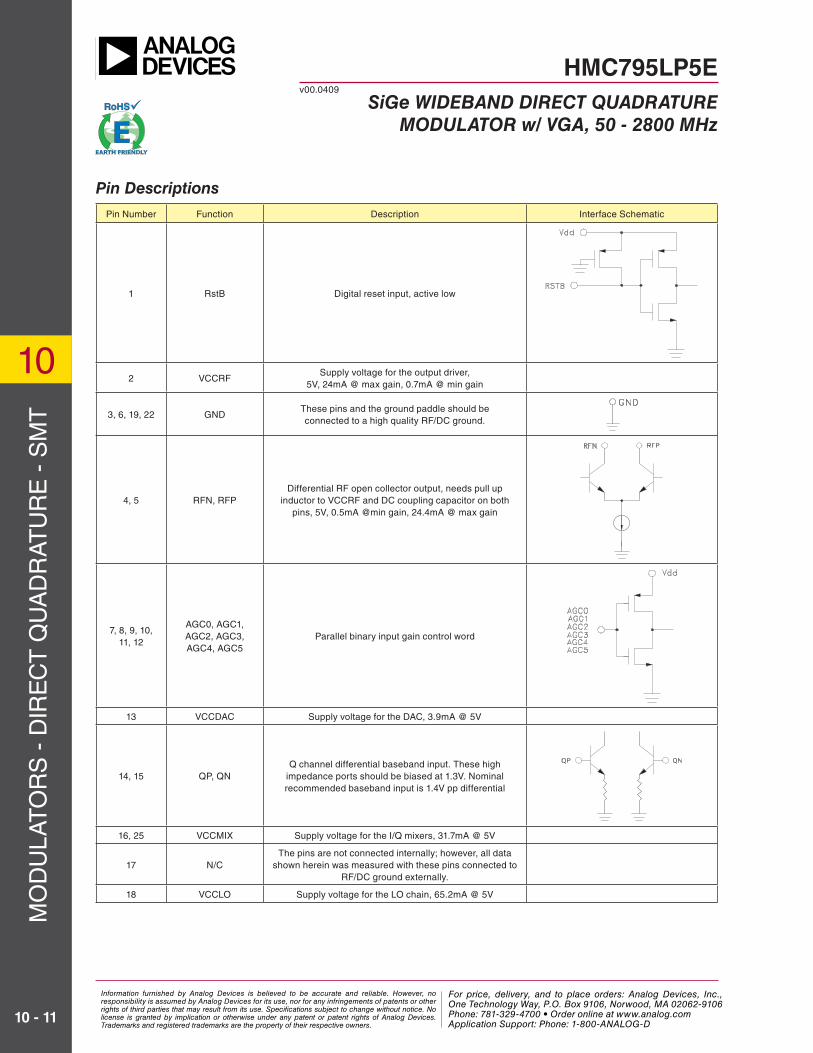
Pin Number Function description interface schematic
1 RstB digital reset input, active low
2 VCCRFsupply voltage for the output driver,
5V, 24mA @ max gain, 0.7mA @ min gain
3, 6, 19, 22 GNdthese pins and the ground paddle should be connected to a high quality RF/dC ground.
4, 5 RFN, RFPdifferential RF open collector output, needs pull up
inductor to VCCRF and dC coupling capacitor on both pins, 5V, 0.5mA @min gain, 24.4mA @ max gain
7, 8, 9, 10, 11, 12
AGC0, AGC1, AGC2, AGC3, AGC4, AGC5
Parallel binary input gain control word
13 VCCdAC supply voltage for the dAC, 3.9mA @ 5V
14, 15 qP, qNq channel differential baseband input. these high
impedance ports should be biased at 1.3V. Nominal recommended baseband input is 1.4V pp differential
16, 25 VCCMiX supply voltage for the i/q mixers, 31.7mA @ 5V
17 N/Cthe pins are not connected internally; however, all data
shown herein was measured with these pins connected to RF/dC ground externally.
18 VCClO supply voltage for the lO chain, 65.2mA @ 5V
Pin descriptions
HMC795LP5Ev00.0409
SiGe Wideband direct QuadratureModulator w/ vGa, 50 - 2800 MHz
Information furnished by Analog Devices is believed to be accurate and reliable. However, no responsibility is assumed by Analog Devices for its use, nor for any infringements of patents or other rights of third parties that may result from its use. Specifications subject to change without notice. No license is granted by implication or otherwise under any patent or patent rights of Analog Devices. Trademarks and registered trademarks are the property of their respective owners.
For price, delivery, and to place orders: Analog Devices, Inc., One Technology Way, P.O. Box 9106, Norwood, MA 02062-9106 Phone: 781-329-4700 • Order online at www.analog.com Application Support: Phone: 1-800-ANALOG-D

For price, delivery, and to place orders, please contact Hittite Microwave Corporation:20 Alpha Road, Chelmsford, MA 01824 Phone: 978-250-3343 Fax: 978-250-3373
Order On-line at www.hittite.com
MO
du
lAt
OR
s -
diR
eC
t q
uA
dR
Atu
Re
- s
Mt
10
10 - 12
Pin descriptions (Continued)
Pin Number Function description interface schematic
20, 21 lOP, lONlO inputs. Need dC decoupling capacitors. the ports
could be driven single ended or differentially
23 VCCBG supply voltage for the bandgap, 4.3mA @ 5V
24 deCOuPle
external bypass decoupling for precision bias circuits, 3.80V
NOte: BiAs ref voltage cannot drive an external load. Must be measured with 10GOhm meter such as Agilent 34410A,
normal 10Mohm dVM will read erroneously.
26, 27 iN, iPi channel differential baseband input. these high
impedance ports should be biased at 1.3V. Nominal recommended baseband input is 1.4V pp differential
28 Vdd3 supply voltage for the digital
29 sdO Main serial port data output
30 sdi Main serial port data input
31 seN Main serial port latch enable input
32 sCK Main serial port clock input
HMC795LP5Ev00.0409
SiGe Wideband direct QuadratureModulator w/ vGa, 50 - 2800 MHz
Information furnished by Analog Devices is believed to be accurate and reliable. However, no responsibility is assumed by Analog Devices for its use, nor for any infringements of patents or other rights of third parties that may result from its use. Specifications subject to change without notice. No license is granted by implication or otherwise under any patent or patent rights of Analog Devices. Trademarks and registered trademarks are the property of their respective owners.
For price, delivery, and to place orders: Analog Devices, Inc., One Technology Way, P.O. Box 9106, Norwood, MA 02062-9106 Phone: 781-329-4700 • Order online at www.analog.com Application Support: Phone: 1-800-ANALOG-D

For price, delivery, and to place orders, please contact Hittite Microwave Corporation:20 Alpha Road, Chelmsford, MA 01824 Phone: 978-250-3343 Fax: 978-250-3373
Order On-line at www.hittite.com
MO
du
lAt
OR
s -
diR
eC
t q
uA
dR
Atu
Re
- s
Mt
10
10 - 13
evaluation Pcb
the circuit board used in the application should use RF circuit design techniques. signal lines should have 50 ohm impedance while the package ground leads and exposed paddle should be connected directly to the ground plane similar to that shown. A sufficient number of via holes should be used to connect the top and bottom ground planes. the evaluation circuit board shown is available from Hittite upon request.
HMC795LP5Ev00.0409
SiGe Wideband direct QuadratureModulator w/ vGa, 50 - 2800 MHz
Information furnished by Analog Devices is believed to be accurate and reliable. However, no responsibility is assumed by Analog Devices for its use, nor for any infringements of patents or other rights of third parties that may result from its use. Specifications subject to change without notice. No license is granted by implication or otherwise under any patent or patent rights of Analog Devices. Trademarks and registered trademarks are the property of their respective owners.
For price, delivery, and to place orders: Analog Devices, Inc., One Technology Way, P.O. Box 9106, Norwood, MA 02062-9106 Phone: 781-329-4700 • Order online at www.analog.com Application Support: Phone: 1-800-ANALOG-D

For price, delivery, and to place orders, please contact Hittite Microwave Corporation:20 Alpha Road, Chelmsford, MA 01824 Phone: 978-250-3343 Fax: 978-250-3373
Order On-line at www.hittite.com
MO
du
lAt
OR
s -
diR
eC
t q
uA
dR
Atu
Re
- s
Mt
10
10 - 14
item description
J1, J10 2 Pin dC Connector
J2, J3, J5 - J8 PCB Mount sMA Connector
J4 12 Pin dC Connector
J9 12 Pin socket Connector
C1, C4, C8, C10, C14, C15, C18, C20, C23, C34, C35, C38
1 µF Capacitor, 0402 Pkg
C2 10 µF Capacitor, 1206 Pkg
C3, C5, C6, C11, C12 4.7 µF Capacitor, 0805 Pkg
C7, C16, C17, C22, C24, C25, C28, C33, C36, C37, C40
1 nF Capacitor, 0402 Pkg
C9, C21 10 nF Capacitor, 0402 Pkg
C13 1.2 nF Capacitor, 0402 Pkg
C19, C27, C32, C41 100 pF Capacitor, 0402 Pkg
C26, C30 - C31, C39, C42 do Not Populate
R1, R4, R21, R24, R27, R30 - R32
100 kOhm Resistor, 0402 Pkg
R2, R3, R5, R6 0 Ohm Resistor, 0402 Pkg
list of Materials for evaluation Pcb [1]
HMC795LP5Ev00.0409
SiGe Wideband direct QuadratureModulator w/ vGa, 50 - 2800 MHz
item description
R7 10 kOhm Resistor, 0402 Pkg
R8, R9, R12 - R20,R22, R23, R25, R26,R28, R29
do Not Populate
R10 4 kOhm Resistor, 0402 Pkg
R11 1 kOhm Resistor, 0402 Pkg
t1, t2 RF transformer
tP1 - tP3 dC Pin
FB1 - FB3 1 kOhms Ferrite Bead, 0805 Pkg
l1, l3 10 nH inductor, 0402 Pkg
l2, l6 4.7 nH inductor, 0402 Pkg
u1 linear Regulator, 3.3V
u2 linear Regulator, 5V
u3 HMC795lP5e Modulator
PCB [2] 125087 eval Board
[1] When requesting an evaluation board, please reference the appropriate PCB number listed in the table “Components for the selected Frequencies”
[2] Circuit Board Material: Arlon 25FR / FR4
tuned Frequency 850 MHz 1950 MHz 2960 MHz
evaluation Board Number 127433 125370 130190
evaluation Kit Number [1] 129934 129935 130186
l2, l6 47 nH 4.7 nH 1.8 nH
l1, l3 27 nH 10 nH 5.6 nH
R29 2.5 kOhms dePOP dePOP
t1 tCN2-14 tCN2-26 tCN2-26
[1] evaluation Kit includes evaluation board, usB controller board, usB cable and evaluation software.
table 9. components for Selected Frequencies
Information furnished by Analog Devices is believed to be accurate and reliable. However, no responsibility is assumed by Analog Devices for its use, nor for any infringements of patents or other rights of third parties that may result from its use. Specifications subject to change without notice. No license is granted by implication or otherwise under any patent or patent rights of Analog Devices. Trademarks and registered trademarks are the property of their respective owners.
For price, delivery, and to place orders: Analog Devices, Inc., One Technology Way, P.O. Box 9106, Norwood, MA 02062-9106 Phone: 781-329-4700 • Order online at www.analog.com Application Support: Phone: 1-800-ANALOG-D

For price, delivery, and to place orders, please contact Hittite Microwave Corporation:20 Alpha Road, Chelmsford, MA 01824 Phone: 978-250-3343 Fax: 978-250-3373
Order On-line at www.hittite.com
MO
du
lAt
OR
s -
diR
eC
t q
uA
dR
Atu
Re
- s
Mt
10
10 - 15
application & evaluation Pcb Schematic
HMC795LP5Ev00.0409
SiGe Wideband direct QuadratureModulator w/ vGa, 50 - 2800 MHz
Information furnished by Analog Devices is believed to be accurate and reliable. However, no responsibility is assumed by Analog Devices for its use, nor for any infringements of patents or other rights of third parties that may result from its use. Specifications subject to change without notice. No license is granted by implication or otherwise under any patent or patent rights of Analog Devices. Trademarks and registered trademarks are the property of their respective owners.
For price, delivery, and to place orders: Analog Devices, Inc., One Technology Way, P.O. Box 9106, Norwood, MA 02062-9106 Phone: 781-329-4700 • Order online at www.analog.com Application Support: Phone: 1-800-ANALOG-D

For price, delivery, and to place orders, please contact Hittite Microwave Corporation:20 Alpha Road, Chelmsford, MA 01824 Phone: 978-250-3343 Fax: 978-250-3373
Order On-line at www.hittite.com
MO
du
lAt
OR
s -
diR
eC
t q
uA
dR
Atu
Re
- s
Mt
10
10 - 16
Theory of Operationthe HMC795lP5e modulator consists of the following functional blocks
1. lO interface2. i/q modulator3. digitally controlled variable gain amplifier4. Gain control dAC5. Bias Circuit6. serial Port interface
lo interface
the lO interface consists of a gain stage followed by a divide by 2 stage that generates two carrier signals in quad-rature which are used to drive the mixers. As a result, the lO path is immune to large variations in the lO signal level and the modulator performance does not vary much with lO power. due to the on chip divider, the input lO frequency must be twice that of the desired carrier frequency. this offers the advantage of significantly lowering carrier feedthrough.
the lO port can be driven differentially or single ended if the unused side is AC grounded. However, when driven single-endedly, the carrier feedthrough and sideband rejection can be degraded by either large 2nd order lO tones, such as when driven by a VCO with a divider output, or, by large half-harmonic tones, such as when driven by a VCO with a doubler output.
the lO interface can be enabled/disabled separately through the serial port interface using Reg01h <0> and can be used to disable the modulator output. the RF output signal is suppressed by 100 dB when only the lO interface is disable and the lO signal itself is suppressed approximately 60 dB. in addition, the lO buffer bias can be increased using Reg02h <7>. this setting is recommended for lO frequencies above 5 GHz.
i/Q Modulator
the HMC795lP5e has two double-balanced mixers, one for the in-phase channel and one for the quadrature chan-nel. the differential baseband inputs (qP, qN, iP, and iN) consist of the bases of NPN transistors, which present a high impedance. the dC common mode voltage at the baseband inputs sets the currents in the two mixer cores. Varying the baseband common mode voltage varies the current in the mixers and affects the overall modulators performance. the recommended dC voltage for the baseband common mode voltage is 1.3V dC, ± 0.1V.
the output of the two mixers are summed together differentially and then used to drive the differential input of the VGA stage. the mixer can be enabled/disabled with Reg01h <1>. the external baseband dC bias also need to be disabled to completely disable the mixers. disabling the mixer enables a weak pull down at the mixer inputs which connects the mixer inputs through a resistive path to ground. this may pull the external input low resulting in large current flow if the external bias is not disabled.
HMC795LP5Ev00.0409
SiGe Wideband direct QuadratureModulator w/ vGa, 50 - 2800 MHz
Information furnished by Analog Devices is believed to be accurate and reliable. However, no responsibility is assumed by Analog Devices for its use, nor for any infringements of patents or other rights of third parties that may result from its use. Specifications subject to change without notice. No license is granted by implication or otherwise under any patent or patent rights of Analog Devices. Trademarks and registered trademarks are the property of their respective owners.
For price, delivery, and to place orders: Analog Devices, Inc., One Technology Way, P.O. Box 9106, Norwood, MA 02062-9106 Phone: 781-329-4700 • Order online at www.analog.com Application Support: Phone: 1-800-ANALOG-D

For price, delivery, and to place orders, please contact Hittite Microwave Corporation:20 Alpha Road, Chelmsford, MA 01824 Phone: 978-250-3343 Fax: 978-250-3373
Order On-line at www.hittite.com
MO
du
lAt
OR
s -
diR
eC
t q
uA
dR
Atu
Re
- s
Mt
10
10 - 17
digitally controlled variable Gain amplifier
the output of the HMC795lP5e is a 6 bit, digitally controlled, variable gain amplifier that can provide very accurate linear- in-dB gain control over a 31.5 dB range in 0.5 dB steps. the VGA also provides relatively constant phase over the entire gain range, as shown in Figure 1. An 11 bit dAC is used to control the VGA. see the Gain Control dAC section for more detail about gain control.
Figure 1. VGA S21 magnitude and phase @ 2 GHz vs attenuation
-30
-25
-20
-15
-10
-5
0
5
10
-130
-120
-110
-100
-90
-80
-70
-60
-50
0 4 8 12 16 20 24 28 32
ATTENUATION (dB)
S21
MA
GN
ITU
DE
(dB
)S
21 PH
AS
E (deg)
PHASEMAGNITUDE
For maximum performance and flexibility, the output ports of the VGA are differential open collectors that require pull up inductors to the positive supply and external matching components. the evaluation board allows for several options for matching. see the Output Matching section for more details.
the VGA can be enabled/disabled separately through the sPi using Reg01h <2>. the ON/OFF isolation of the VGA is greater than 60 dB for RF output frequencies up to 2.5 GHz.
Gain control dac
An 11 bit dAC is used to control the VGA for linear-in-dB gain control, Figure 2 shows the control for the dAC.. the dAC is normally controlled by a look up table (lut) that is in turn, controlled by the 6 bit parallel port. the values of the look up table are fixed to give 0.5 dB steps over a 31.5 dB gain range.
Figure 2. Simplified DAC control diagram
For increased flexibility, there are three methods to control the dAC and VGA gain.
1. Parallel Mode use the 6 bit parallel port to provide fixed 0.5 dB gain steps. in this mode the dAC is controlled by a look up table with 64 states that map the 6 bit parallel port to fixed 11-Bit gain words for each state. the values of the lut are fixed to give nominally 0.5 dB attenuation steps over a 31.5 dB gain range.
HMC795LP5Ev00.0409
SiGe Wideband direct QuadratureModulator w/ vGa, 50 - 2800 MHz
Information furnished by Analog Devices is believed to be accurate and reliable. However, no responsibility is assumed by Analog Devices for its use, nor for any infringements of patents or other rights of third parties that may result from its use. Specifications subject to change without notice. No license is granted by implication or otherwise under any patent or patent rights of Analog Devices. Trademarks and registered trademarks are the property of their respective owners.
For price, delivery, and to place orders: Analog Devices, Inc., One Technology Way, P.O. Box 9106, Norwood, MA 02062-9106 Phone: 781-329-4700 • Order online at www.analog.com Application Support: Phone: 1-800-ANALOG-D

For price, delivery, and to place orders, please contact Hittite Microwave Corporation:20 Alpha Road, Chelmsford, MA 01824 Phone: 978-250-3343 Fax: 978-250-3373
Order On-line at www.hittite.com
MO
du
lAt
OR
s -
diR
eC
t q
uA
dR
Atu
Re
- s
Mt
10
10 - 18
2. Correction Mode use the sPi port in conjunction with the 6 bit parallel port to apply a 4 bit, 2’s complement, correction factor to any attenuation step. this option can be used to compensate the gain control for systematic variations in the transmit chain by adding negative or positive correction factors to any of the fixed lut values to either slightly increase or decrease the gain step for that particulate state. this mode requires the host controller to write the desired corrections to the sPi after the chip is powered up. the correction factors are then applied to the desired gain steps when ever the parallel port gain control changes, until the chip is powered down.
the 4 bit, 2’s compliment, correction factor for each line in the lut are set by Reg4h to Reg13h. the correction factor for 0 dB attenuation (line 0) is set in Reg4h <3:0>, 0.5 dB (line 1) is set by Reg4h <7:4>, 1.0 dB (line 2) by Reg4h<11:8> and so on until Reg13h <15:12> which sets the correc-tion factor for 31.5 dB attenuation. if more adjustment is needed, the lut correction values can be increased by a factor of 2, 3, or 4 times by using Reg2h <15:8>. Reg2h <9:8> sets the multiplication factor for the first quadrant of the lut, lines 0 to 15, <11:10> for lines 16 to 31, <13:12> for lines 32 to 47 and <15:14> for the last quadrant, lines 48 to 63. the correction in dB can be estimated by
COR(dB) = 10 · log10 1 +[( )-1 ](CORword · mult)LUTword
where mult is the correction multiplication factor, and CORword and lutword are the decimal equivalent of the binary correction and lut word. An expression for determining the lutword is given in the bypass mode section below. Figures 3, 4 and 5 show the range of correction in dB for 4 dB, 16 dB and 31.5 dB attenuation and Figure 6 shows the output power versus attenuation for no correction, maximum positive and maximum negative correction applied to all states in the lut. the lut value for 0 dB attenuation can only be decreased since it already at maximum. increasing the word value will cause an overflow resulting in maximum attenuation instead.
Figure 3. Attenuation Change from 4 dB Attenuation vs. LUT Correction Word over Different
Multiplication Factors
Figure 4. Attenuation Change from 16 dB Attenuation vs. LUT Correction Word over Different
Multiplication Factors
-0.3
-0.2
-0.1
0
0.1
0.2
0.3
-8 -6 -4 -2 0 2 4 6 8
LUT CORRECTION WORD
AT
TE
NU
AT
ION
CH
AN
GE
(dB
)
X1
X4X3
X2
-1
-0.5
0
0.5
1
-8 -6 -4 -2 0 2 4 6 8
LUT CORRECTION WORD
AT
TE
NU
AT
ION
CH
AN
GE
(dB
)
X1
X4X3
X2
HMC795LP5Ev00.0409
SiGe Wideband direct QuadratureModulator w/ vGa, 50 - 2800 MHz
Information furnished by Analog Devices is believed to be accurate and reliable. However, no responsibility is assumed by Analog Devices for its use, nor for any infringements of patents or other rights of third parties that may result from its use. Specifications subject to change without notice. No license is granted by implication or otherwise under any patent or patent rights of Analog Devices. Trademarks and registered trademarks are the property of their respective owners.
For price, delivery, and to place orders: Analog Devices, Inc., One Technology Way, P.O. Box 9106, Norwood, MA 02062-9106 Phone: 781-329-4700 • Order online at www.analog.com Application Support: Phone: 1-800-ANALOG-D

For price, delivery, and to place orders, please contact Hittite Microwave Corporation:20 Alpha Road, Chelmsford, MA 01824 Phone: 978-250-3343 Fax: 978-250-3373
Order On-line at www.hittite.com
MO
du
lAt
OR
s -
diR
eC
t q
uA
dR
Atu
Re
- s
Mt
10
10 - 19
HMC795LP5Ev00.0409
SiGe Wideband direct QuadratureModulator w/ vGa, 50 - 2800 MHz
Figure 5. Attenuation Change from 31.5 dB Attenuation vs. LUT Correction Word over Different
Multiplication Factors
Figure 6. Output Power @ 850 MHz vs. VGA Attenuation for no Correction, Maximum Positive &
Maximum Negative Correction Values
-8
-6
-4
-2
0
2
4
6
8
-8 -6 -4 -2 0 2 4 6 8
LUT CORRECTION WORD
AT
TE
NU
AT
ION
CH
AN
GE
(dB
)
X1
X4X3
X2
-30
-25
-20
-15
-10
-5
0
5
10
0 4 8 12 16 20 24 28 32
ATTENUATION (dB)
OU
TP
UT
PO
WE
R (
dBm
)
MAX +VECORRECTION
MAX -VECORRECTION
3. Bypass Mode. use the sPi port to bypass the parallel port and lut completely. in this mode Reg2h<4> is set to enable the bypass mode. the host controller can then write the desired gain word to the sPi using Reg3h<10:0> for each and every desired gain change. the input word can be determined from the desired gain (in dB) by
LUTword(10:0) = dec2bin[round[(211 - 1) · 10(-attn)/20]]
and is plotted in Figure 7. in the this mode it is possible to use much lower attenuation steps over a reduced gain control range. the limit for reliable attenuation steps is 0.1 dB with a gain control range of approximately 22 dB.
0
4
8
12
16
20
24
28
32
0 500 1000 1500 2000
LUT WORD
AT
TE
NU
AT
ION
(dB
)
Figure 7. Attenuation vs. LUT word
the dAC can be enabled/disabled separately through the serial port interface using bit 3 of register 01h. disabling the dAC will also disable the VGA.
Information furnished by Analog Devices is believed to be accurate and reliable. However, no responsibility is assumed by Analog Devices for its use, nor for any infringements of patents or other rights of third parties that may result from its use. Specifications subject to change without notice. No license is granted by implication or otherwise under any patent or patent rights of Analog Devices. Trademarks and registered trademarks are the property of their respective owners.
For price, delivery, and to place orders: Analog Devices, Inc., One Technology Way, P.O. Box 9106, Norwood, MA 02062-9106 Phone: 781-329-4700 • Order online at www.analog.com Application Support: Phone: 1-800-ANALOG-D
For price, delivery, and to place orders, please contact Hittite Microwave Corporation:20 Alpha Road, Chelmsford, MA 01824 Phone: 978-250-3343 Fax: 978-250-3373
Order On-line at www.hittite.com
MO
du
lAt
OR
s -
diR
eC
t q
uA
dR
Atu
Re
- s
Mt
10
10 - 20
HMC795LP5Ev00.0409
SiGe Wideband direct QuadratureModulator w/ vGa, 50 - 2800 MHz
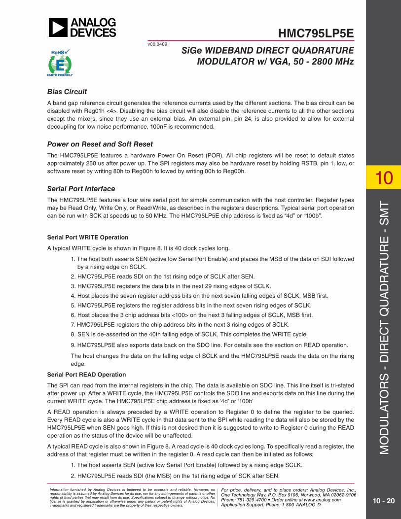
bias circuit
A band gap reference circuit generates the reference currents used by the different sections. the bias circuit can be disabled with Reg01h <4>. disabling the bias circuit will also disable the reference currents to all the other sections except the mixers, since they use an external bias. An external pin, pin 24, is also provided to allow for external decoupling for low noise performance, 100nF is recommended.
Power on reset and Soft reset
the HMC795lP5e features a hardware Power On Reset (POR). All chip registers will be reset to default states approximately 250 us after power up. the sPi registers may also be hardware reset by holding RstB, pin 1, low, or software reset by writing 80h to Reg00h followed by writing 00h to Reg00h.
Serial Port interface
the HMC795lP5e features a four wire serial port for simple communication with the host controller. Register types may be Read Only, Write Only, or Read/Write, as described in the registers descriptions. typical serial port operation can be run with sCK at speeds up to 50 MHz. the HMC795lP5e chip address is fixed as “4d” or “100b”.
Serial Port WRITE Operation
A typical WRite cycle is shown in Figure 8. it is 40 clock cycles long.
1. the host both asserts seN (active low serial Port enable) and places the MsB of the data on sdi followed by a rising edge on sClK.
2. HMC795lP5e reads sdi on the 1st rising edge of sClK after seN.
3. HMC795lP5e registers the data bits in the next 29 rising edges of sClK.
4. Host places the seven register address bits on the next seven falling edges of sClK, MsB first.
5. HMC795lP5e registers the register address bits in the next seven rising edges of sClK.
6. Host places the 3 chip address bits <100> on the next 3 falling edges of sClK, MsB first.
7. HMC795lP5e registers the chip address bits in the next 3 rising edges of sClK.
8. seN is de-asserted on the 40th falling edge of sClK. this completes the WRite cycle.
9. HMC795lP5e also exports data back on the sdO line. For details see the section on ReAd operation.
the host changes the data on the falling edge of sClK and the HMC795lP5e reads the data on the rising edge.
Serial Port READ Operation
the sPi can read from the internal registers in the chip. the data is available on sdO line. this line itself is tri-stated after power up. After a WRite cycle, the HMC795lP5e controls the sdO line and exports data on this line during the current WRite cycle. the HMC795lP5e chip address is fixed as ‘4d’ or ‘100b’
A ReAd operation is always preceded by a WRite operation to Register 0 to define the register to be queried. every ReAd cycle is also a WRite cycle in that data sent to the sPi while reading the data will also be stored by the HMC795lP5e when seN goes high. if this is not desired then it is suggested to write to Register 0 during the ReAd operation as the status of the device will be unaffected.
A typical ReAd cycle is also shown in Figure 8. A read cycle is 40 clock cycles long. to specifically read a register, the address of that register must be written in the register 0. A read cycle can then be initiated as follows;
1. the host asserts seN (active low serial Port enable) followed by a rising edge sClK.
2. HMC795lP5e reads sdi (the MsB) on the 1st rising edge of sCK after seN.
Information furnished by Analog Devices is believed to be accurate and reliable. However, no responsibility is assumed by Analog Devices for its use, nor for any infringements of patents or other rights of third parties that may result from its use. Specifications subject to change without notice. No license is granted by implication or otherwise under any patent or patent rights of Analog Devices. Trademarks and registered trademarks are the property of their respective owners.
For price, delivery, and to place orders: Analog Devices, Inc., One Technology Way, P.O. Box 9106, Norwood, MA 02062-9106 Phone: 781-329-4700 • Order online at www.analog.com Application Support: Phone: 1-800-ANALOG-D
For price, delivery, and to place orders, please contact Hittite Microwave Corporation:20 Alpha Road, Chelmsford, MA 01824 Phone: 978-250-3343 Fax: 978-250-3373
Order On-line at www.hittite.com
MO
du
lAt
OR
s -
diR
eC
t q
uA
dR
Atu
Re
- s
Mt
10
10 - 21
HMC795LP5Ev00.0409
SiGe Wideband direct QuadratureModulator w/ vGa, 50 - 2800 MHz
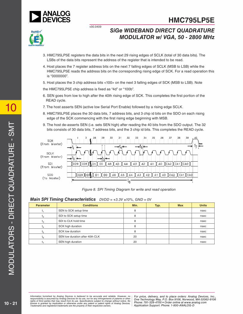
3. HMC795lP5e registers the data bits in the next 29 rising edges of sClK (total of 30 data bits). the lsBs of the data bits represent the address of the register that is intended to be read.
4. Host places the 7 register address bits on the next 7 falling edges of sClK (MsB to lsB) while the HMC795lP5e reads the address bits on the corresponding rising edge of sCK. For a read operation this is “0000000”.
5. Host places the 3 chip address bits <100> on the next 3 falling edges of sCK (MsB to lsB). Note
the HMC795lP5e chip address is fixed as “4d” or “100b”.
6. seN goes from low to high after the 40th rising edge of sCK. this completes the first portion of the ReAd cycle.
7. the host asserts seN (active low serial Port enable) followed by a rising edge sClK.
8. HMC795lP5e places the 30 data bits, 7 address bits, and 3 chip id bits on the sdO on each rising edge of the sCK commencing with the first rising edge beginning with MsB.
9. the host de-asserts seN (i.e. sets seN high) after reading the 40 bits from the sdO output. the 32 bits consists of 30 data bits, 7 address bits, and the 3 chip id bits. this completes the ReAd cycle.
Figure 8. SPI Timing Diagram for write and read operation
Main SPi timing characteristics DVDD = +3.3V ±10%, GND = 0V
Parameter Conditions Min. Typ. Max Units
t1 seN to sCK setup time 8 nsec
t2 sdi to sCK setup time 8 nsec
t3 sdi to ClK hold time 8 nsec
t4 sCK high duration 8 nsec
t5 sCK low duration 8 nsec
t6 seN low duration after 40th ClK 20 nsec
t7 seN high duration 20 nsec
Information furnished by Analog Devices is believed to be accurate and reliable. However, no responsibility is assumed by Analog Devices for its use, nor for any infringements of patents or other rights of third parties that may result from its use. Specifications subject to change without notice. No license is granted by implication or otherwise under any patent or patent rights of Analog Devices. Trademarks and registered trademarks are the property of their respective owners.
For price, delivery, and to place orders: Analog Devices, Inc., One Technology Way, P.O. Box 9106, Norwood, MA 02062-9106 Phone: 781-329-4700 • Order online at www.analog.com Application Support: Phone: 1-800-ANALOG-D

For price, delivery, and to place orders, please contact Hittite Microwave Corporation:20 Alpha Road, Chelmsford, MA 01824 Phone: 978-250-3343 Fax: 978-250-3373
Order On-line at www.hittite.com
MO
du
lAt
OR
s -
diR
eC
t q
uA
dR
Atu
Re
- s
Mt
10
10 - 22
HMC795LP5Ev00.0409
SiGe Wideband direct QuadratureModulator w/ vGa, 50 - 2800 MHz
output Matching
the output ports of the VGA are differential open collectors that require pull up inductors to the positive supply and external matching components. the evaluation board uses a 2:1 impedance transformer to convert the differential output to single ended for evaluation purposes. three options are available for the evaluation board, each with different matching components, one for 850 MHz, one for 1950 MHz, and another for 2690 MHz. When requesting an evaluation board, please reference the appropriate PCB number listed in the table “Components for the selected Frequencies”
there are a number of ways to match the RF output of the HMC795lP5e for optimum performance. the most basic method is to use a 50 Ω resistor to Vcc and a 1 nF dc bypass capacitor connected in series as shown Figure 9(a). this option provides a good broadband match, see Figure 10, but limits the maximum output power, compared to a narrow band match, see Figure 11. single-ended operation is possible by using a transformer, which can limit the bandwidth, as seen in the output power plot, or by using only one side of the differential output. However, biasing for the unused side is still required. For best performance it is recommended to terminate the unused side with the same matching and load impedance as the used side, see Figure 9(b). Output power is generally reduced by 2 to 3 dB for single-ended operation, as shown in Figure 11.
Figure 9. Simple output matching network
-40
-35
-30
-25
-20
-15
-10
-5
0
0 500 1000 1500 2000 2500 3000
FREQUENCY (MHz)
RE
TU
RN
LO
SS
(dB
)
NARROW BANDDIFFERENTIAL
WIDE BANDSINGLE ENDED
WIDE BAND
DIFFERENTIAL [1]
WIDE BAND
DIFFERENTIAL [2]
-10
-5
0
5
10
0 500 1000 1500 2000 2500 3000 3500
FREQUENCY (MHz)
OU
TP
UT
PO
WE
R (
dBm
)
NARROW BANDDIFFERENTIAL
WIDE BANDSINGLE ENDED
WIDE BAND
DIFFERENTIAL [1]
WIDE BAND
DIFFERENTIAL [2]
Figure 10. Output Return Loss for Various Matching Options [1] With tCN2-14 transformer
[2] With tCN2-26 transformer
Figure 11. Output Power for Various Matching Options [1] With tCN2-14 transformer
[2] With tCN2-26 transformer
A narrow band solution, with higher output power, is possible by using a simple l-match network, as shown in Figure 12. A shunt resistor is included to control the q of the matching network and sets the output power of the HMC795lP5e. Consequently a low value resistor will result in a broadband match but lower output power than a high value resistor. the table below provides recommend component values for various output frequencies with a bandwidth of approximately 5-10%. it is also possible to use an lC matching network where l2 is removed and the dC blocking capacitor is used as a matching component. experiments show that the output power is reduced approximately 1 -2 dB though and that values for the capacitors become unrealistic (< 500 fF) above 2 GHz.
Information furnished by Analog Devices is believed to be accurate and reliable. However, no responsibility is assumed by Analog Devices for its use, nor for any infringements of patents or other rights of third parties that may result from its use. Specifications subject to change without notice. No license is granted by implication or otherwise under any patent or patent rights of Analog Devices. Trademarks and registered trademarks are the property of their respective owners.
For price, delivery, and to place orders: Analog Devices, Inc., One Technology Way, P.O. Box 9106, Norwood, MA 02062-9106 Phone: 781-329-4700 • Order online at www.analog.com Application Support: Phone: 1-800-ANALOG-D

For price, delivery, and to place orders, please contact Hittite Microwave Corporation:20 Alpha Road, Chelmsford, MA 01824 Phone: 978-250-3343 Fax: 978-250-3373
Order On-line at www.hittite.com
MO
du
lAt
OR
s -
diR
eC
t q
uA
dR
Atu
Re
- s
Mt
10
10 - 23
HMC795LP5Ev00.0409
SiGe Wideband direct QuadratureModulator w/ vGa, 50 - 2800 MHz
Figure 12. Simple output matching network
recommending Matching components450 MHz 850 MHz 1450 MHz 1850 MHz 1950 MHz 2400 MHz 2500 MHz 2690
l1 270 nH 47 nH 12 nH 5.6 nH 4.7 nH 2.7 nH 2.2 nH 1.8 nH
l2 82 nH 27 nh 12 nH 12 nH 10 nH 6.8 nH 5.6 nH 5.6 nH
R1 - 2.4K 2.4K - - - - -
t1 Bypassed tCN2-14 tCN2-14 tCN2-26 tCN2-26 tCN2-26 tCN2-26 tCN2-26
dac Modulator interface network
the HMC795lP5eis capable of interfacing with a variety of popular d/A Convertors. Most dAC have differential outputs with a source or sink current of 0 mA to 20 mA. However, most dACs require a different output compliance voltage than that of the dC input bias level for the HMC795lP5e. A passive interface network can be used to transform the common-mode voltage of the dAC to the desired dC input bias of the modulator of 1.3V. Figures 13 and 14 show the interface network for two different topologies.
1. topology 1. dAC Vcm > HMC795lP5e Vcm. this topology is used shift the dAC output common mode voltage down to the required dC level at the modulator input.
2. topology 2. dAC Vcm < HMC795lP5e Vcm. this topology is used shift the dAC output common mode voltage up to the required dC level at the modulator input.
the resistive level-shifting network is not frequency sensitive but the resistive divider network inherent in the network attenuates the baseband signal. the bypass capacitors shown Figures 13 and 14 will eliminate the attenuation for frequencies greater than 3 kHz. either topology can be used on the HMC795lP5e evaluation board.
Figure 13. DAC Interface network topology 1
Information furnished by Analog Devices is believed to be accurate and reliable. However, no responsibility is assumed by Analog Devices for its use, nor for any infringements of patents or other rights of third parties that may result from its use. Specifications subject to change without notice. No license is granted by implication or otherwise under any patent or patent rights of Analog Devices. Trademarks and registered trademarks are the property of their respective owners.
For price, delivery, and to place orders: Analog Devices, Inc., One Technology Way, P.O. Box 9106, Norwood, MA 02062-9106 Phone: 781-329-4700 • Order online at www.analog.com Application Support: Phone: 1-800-ANALOG-D

For price, delivery, and to place orders, please contact Hittite Microwave Corporation:20 Alpha Road, Chelmsford, MA 01824 Phone: 978-250-3343 Fax: 978-250-3373
Order On-line at www.hittite.com
MO
du
lAt
OR
s -
diR
eC
t q
uA
dR
Atu
Re
- s
Mt
10
10 - 24
HMC795LP5Ev00.0409
SiGe Wideband direct QuadratureModulator w/ vGa, 50 - 2800 MHz
Figure 14. DAC Interface network topology 2
dac interface network valuesTopology 1 Topology 2
dAC Vcm 3.3 0.5
R1 62 Ω 36 Ω
R2 130 Ω 200 Ω
R3 82 Ω 910 Ω
Register Map
reg 01h - enable / control registerBit Name Width Default Description
[0] enlO 1 1 enables lO path
[1] enMix 1 1enables Mixer lO bias- see i/q modulator section for more detail
[2] endrvr 1 1 enables output driver
[3] endAC 1 1 enables gain control dAC
[4] enBias 1 1 enables bandgap and bias
reg 02h - Function registerBit Name Width Default Description
[1:0} Reserved 2 00 Reserved
[3:2] Reserved 2 00 Reserved
[4] lut Bypass 1 0Allows direct control of the gain control dAC via the dAC word in Reg03
[6:5] Reserved 2 00 Reserved
[7] lO Buffer Bias 1 0increases the lO buffer bias current by approximately 7.5mA
[9:8] mult_0 2 00
Multiplication factor for correction to attenuation settings 0 to 7.5dB00: x1 (default)01: x210: x311: x4
Information furnished by Analog Devices is believed to be accurate and reliable. However, no responsibility is assumed by Analog Devices for its use, nor for any infringements of patents or other rights of third parties that may result from its use. Specifications subject to change without notice. No license is granted by implication or otherwise under any patent or patent rights of Analog Devices. Trademarks and registered trademarks are the property of their respective owners.
For price, delivery, and to place orders: Analog Devices, Inc., One Technology Way, P.O. Box 9106, Norwood, MA 02062-9106 Phone: 781-329-4700 • Order online at www.analog.com Application Support: Phone: 1-800-ANALOG-D

For price, delivery, and to place orders, please contact Hittite Microwave Corporation:20 Alpha Road, Chelmsford, MA 01824 Phone: 978-250-3343 Fax: 978-250-3373
Order On-line at www.hittite.com
MO
du
lAt
OR
s -
diR
eC
t q
uA
dR
Atu
Re
- s
Mt
10
10 - 25
HMC795LP5Ev00.0409
SiGe Wideband direct QuadratureModulator w/ vGa, 50 - 2800 MHz
reg 02h - Function registerBit Name Width Default Description
[11:10] mult_1 2 00
Multiplication factor for lines 16 - 31 of lut (2nd quadrant)00: x1 (nom)01: x210: x311: x4
[13:12] mult_2 2 00
Multiplication factor for correction to attenuation settings 16 to 23.5dB00: x1 (default)01: x210: x311: x4
[15:13] mult_3 2 00
Multiplication factor for correction to attenuation settings 24 - 31.5dB00: x1 (default)01: x210: x311: x4
[17:16] Reserved 2 00 Reserved
[21:18] Reserved 4 0000 Reserved
reg 03h - Gain controlBit Name Width Default Description
[10:0] idac 11 000h
Gain control dAC input word. lut bypass bit in register 2h must be enabled.
Gain control dAC word consists of an 11bit input word where 7FFh is maximum gain and 36h corresponds to minimum gain.
Neglecting dAC error, the input word can be determined from the desired gain (in dB) as follows:
idac<10:0>=dec2bin(round((2^(11) 1)*10^(gain/20)))
reg 04h - lut correction 0 - 3
LUT correction values below can also be multiplied by 1,2,3, or 4 if more correction is needed. Multiplication factor for LUT lines 0 -15 (attenuation 0 to 7.5 dB) is set in Reg2 by bits mult_0 [9:8]
Bit Name Width Default Description
[3:0] lut_0 4 0000 2’s complement 4bit correction to lut line 0 (attenuation 0 dB)
[7:4] lut_1 4 0000 2’s complement 4-bit correction to lut line 1 (attenuation 0.5 dB)
[11:8] lut_2 4 0000 2’s complement 4-bit correction to lut line 2 (attenuation 1 dB)
[15:12] lut_3 4 0000 2’s complement 4-bit correction to lut line 3 (attenuation 1.5 dB)
Information furnished by Analog Devices is believed to be accurate and reliable. However, no responsibility is assumed by Analog Devices for its use, nor for any infringements of patents or other rights of third parties that may result from its use. Specifications subject to change without notice. No license is granted by implication or otherwise under any patent or patent rights of Analog Devices. Trademarks and registered trademarks are the property of their respective owners.
For price, delivery, and to place orders: Analog Devices, Inc., One Technology Way, P.O. Box 9106, Norwood, MA 02062-9106 Phone: 781-329-4700 • Order online at www.analog.com Application Support: Phone: 1-800-ANALOG-D

For price, delivery, and to place orders, please contact Hittite Microwave Corporation:20 Alpha Road, Chelmsford, MA 01824 Phone: 978-250-3343 Fax: 978-250-3373
Order On-line at www.hittite.com
MO
du
lAt
OR
s -
diR
eC
t q
uA
dR
Atu
Re
- s
Mt
10
10 - 26
HMC795LP5Ev00.0409
SiGe Wideband direct QuadratureModulator w/ vGa, 50 - 2800 MHz
reg 05h - lut correction 4 - 7
LUT correction values below can also be multiplied by 1,2,3, or 4 if more correction is needed. Multiplication factor for LUT lines 0 -15 (attenuation 0 to 7.5 dB) is set in Reg2 by bits mult_0 [9:8]
Bit Name Width Default Description
[3:0] lut_4 4 0000 2’s complement 4-bit correction to lut line 4 (attenuation 2 dB)
[7:4] lut_5 4 0000 2’s complement 4-bit correction to lut line 5 (attenuation 2.5 dB)
[11:8] lut_6 4 0000 2’s complement 4-bit correction to lut line 6 (attenuation 3 dB)
[15:12] lut_7 4 0000 2’s complement 4-bit correction to lut line 7 (attenuation 3.5 dB)
reg 06h - lut correction 8 - 11
LUT correction values below can also be multiplied by 1,2,3, or 4 if more correction is needed. Multiplication factor for LUT lines 0 -15 (attenuation 0 to 7.5 dB) is set in Reg2 by bits mult_0 [9:8]
Bit Name Width Default Description
[3:0] lut_8 4 0000 2’s complement 4-bit correction to lut line 8 (attenuation 4 dB)
[7:4] lut_9 4 0000 2’s complement 4-bit correction to lut line 9 (attenuation 4.5 dB)
[11:8] lut_10 4 0000 2’s complement 4-bit correction to lut line 10 (attenuation 5 dB)
[15:12] lut_11 4 0000 2’s complement 4-bit correction to lut line 11 (attenuation 5.5 dB)
reg 07h - lut correction 12 - 15
LUT correction values below can also be multiplied by 1,2,3, or 4 if more correction is needed. Multiplication factor for LUT lines 0 -15 (attenuation 0 to 7.5 dB) is set in Reg2 by bits mult_0 [9:8]
Bit Name Width Default Description
[3:0] lut_12 4 0000 2’s complement 4-bit correction to lut line 12 (attenuation 6 dB)
[7:4] lut_13 4 0000 2’s complement 4-bit correction to lut line 13 (attenuation 6.5 dB)
[11:8] lut_14 4 0000 2’s complement 4-bit correction to lut line 14 (attenuation 7 dB)
[15:12] lut_15 4 0000 2’s complement 4-bit correction to lut line 15 (attenuation 7.5 dB)
reg 08h - lut correction 16 - 19
LUT correction values below can also be multiplied by 1,2,3, or 4 if more correction is needed. Multiplication factor for LUT lines 16 - 31 (attenuation 8 to 15.5 dB) is set in Reg2 by bits mult_0 [11:10]
Bit Name Width Default Description
[3:0] lut_16 4 0000 2’s complement 4-bit correction to lut line 16 (attenuation 8 dB)
[7:4] lut_17 4 0000 2’s complement 4-bit correction to lut line 17 (attenuation 8.5 dB)
[11:8] lut_18 4 0000 2’s complement 4-bit correction to lut line 18 (attenuation 9 dB)
[15:12] lut_19 4 0000 2’s complement 4-bit correction to lut line 19 (attenuation 9.5 dB)
Information furnished by Analog Devices is believed to be accurate and reliable. However, no responsibility is assumed by Analog Devices for its use, nor for any infringements of patents or other rights of third parties that may result from its use. Specifications subject to change without notice. No license is granted by implication or otherwise under any patent or patent rights of Analog Devices. Trademarks and registered trademarks are the property of their respective owners.
For price, delivery, and to place orders: Analog Devices, Inc., One Technology Way, P.O. Box 9106, Norwood, MA 02062-9106 Phone: 781-329-4700 • Order online at www.analog.com Application Support: Phone: 1-800-ANALOG-D

For price, delivery, and to place orders, please contact Hittite Microwave Corporation:20 Alpha Road, Chelmsford, MA 01824 Phone: 978-250-3343 Fax: 978-250-3373
Order On-line at www.hittite.com
MO
du
lAt
OR
s -
diR
eC
t q
uA
dR
Atu
Re
- s
Mt
10
10 - 27
HMC795LP5Ev00.0409
SiGe Wideband direct QuadratureModulator w/ vGa, 50 - 2800 MHz
reg 09h - lut correction 20 - 23
LUT correction values below can also be multiplied by 1,2,3, or 4 if more correction is needed. Multiplication factor for LUT lines 16 - 31 (attenuation 8 to 15.5 dB) is set in Reg2 by bits mult_0 [11:10]
Bit Name Width Default Description
[3:0] lut_20 4 0000 2’s complement 4-bit correction to lut line 20 (attenuation 10 dB)
[7:4] lut_21 4 0000 2’s complement 4-bit correction to lut line 21 (attenuation 10.5 dB)
[11:8] lut_22 4 0000 2’s complement 4-bit correction to lut line 22 (attenuation 11 dB)
[15:12] lut_23 4 0000 2’s complement 4-bit correction to lut line 23 (attenuation 11.5 dB)
reg 0ah - lut correction 24 - 27
LUT correction values below can also be multiplied by 1,2,3, or 4 if more correction is needed. Multiplication factor for LUT lines 16 - 31 (attenuation 8 to 15.5 dB) is set in Reg2 by bits mult_0 [11:10]
Bit Name Width Default Description
[3:0] lut_24 4 0000 2’s complement 4-bit correction to lut line 24 (attenuation 12 dB)
[7:4] lut_25 4 0000 2’s complement 4-bit correction to lut line 25 (attenuation 12.5 dB)
[11:8] lut_26 4 0000 2’s complement 4-bit correction to lut line 26 (attenuation 13 dB)
[15:12] lut_27 4 0000 2’s complement 4-bit correction to lut line 27 (attenuation 13.5 dB)
reg 0bh - lut correction 28 - 31
LUT correction values below can also be multiplied by 1,2,3, or 4 if more correction is needed. Multiplication factor for LUT lines 16 - 31 (attenuation 8 to 15.5 dB) is set in Reg2 by bits mult_0 [11:10]
Bit Name Width Default Description
[3:0] lut_28 4 0000 2’s complement 4-bit correction to lut line 28 (attenuation 14 dB)
[7:4] lut_29 4 0000 2’s complement 4-bit correction to lut line 29 (attenuation 14.5 dB)
[11:8] lut_30 4 0000 2’s complement 4-bit correction to lut line 30 (attenuation 15 dB)
[15:12] lut_31 4 0000 2’s complement 4-bit correction to lut line 31 (attenuation 15.5 dB)
reg 0ch - lut correction 32 - 35
LUT correction values below can also be multiplied by 1,2,3, or 4 if more correction is needed. Multiplication factor for LUT lines 32 - 47 (attenuation 15 to 23.5 dB) is set in Reg2 by bits mult_0 [13:12]
Bit Name Width Default Description
[3:0] lut_32 4 0000 2’s complement 4-bit correction to lut line 32 (attenuation 16 dB)
[7:4] lut_33 4 0000 2’s complement 4-bit correction to lut line 33 (attenuation 16.5 dB)
[11:8] lut_34 4 0000 2’s complement 4-bit correction to lut line 34 (attenuation 17 dB)
[15:12] lut_35 4 0000 2’s complement 4-bit correction to lut line 35 (attenuation 17.5 dB)
Information furnished by Analog Devices is believed to be accurate and reliable. However, no responsibility is assumed by Analog Devices for its use, nor for any infringements of patents or other rights of third parties that may result from its use. Specifications subject to change without notice. No license is granted by implication or otherwise under any patent or patent rights of Analog Devices. Trademarks and registered trademarks are the property of their respective owners.
For price, delivery, and to place orders: Analog Devices, Inc., One Technology Way, P.O. Box 9106, Norwood, MA 02062-9106 Phone: 781-329-4700 • Order online at www.analog.com Application Support: Phone: 1-800-ANALOG-D

For price, delivery, and to place orders, please contact Hittite Microwave Corporation:20 Alpha Road, Chelmsford, MA 01824 Phone: 978-250-3343 Fax: 978-250-3373
Order On-line at www.hittite.com
MO
du
lAt
OR
s -
diR
eC
t q
uA
dR
Atu
Re
- s
Mt
10
10 - 28
HMC795LP5Ev00.0409
SiGe Wideband direct QuadratureModulator w/ vGa, 50 - 2800 MHz
reg 0dh - lut correction 36 - 39
LUT correction values below can also be multiplied by 1,2,3, or 4 if more correction is needed. Multiplication factor for LUT lines 32 - 47 (attenuation 15 to 23.5 dB) is set in Reg2 by bits mult_0 [13:12]
Bit Name Width Default Description
[3:0] lut_36 4 0000 2’s complement 4-bit correction to lut line 36 (attenuation 18 dB)
[7:4] lut_37 4 0000 2’s complement 4-bit correction to lut line 37 (attenuation 18.5 dB)
[11:8] lut_38 4 0000 2’s complement 4-bit correction to lut line 38 (attenuation 19 dB)
[15:12] lut_39 4 0000 2’s complement 4-bit correction to lut line 39 (attenuation 19.5 dB)
reg 0eh - lut correction 40 - 43
LUT correction values below can also be multiplied by 1,2,3, or 4 if more correction is needed. Multiplication factor for LUT lines 32 - 47 (attenuation 15 to 23.5 dB) is set in Reg2 by bits mult_0 [13:12]
Bit Name Width Default Description
[3:0] lut_40 4 0000 2’s complement 4-bit correction to lut line 40 (attenuation 20 dB)
[7:4] lut_41 4 0000 2’s complement 4-bit correction to lut line 41 (attenuation 20.5 dB)
[11:8] lut_42 4 0000 2’s complement 4-bit correction to lut line 42 (attenuation 21 dB)
[15:12] lut_43 4 0000 2’s complement 4-bit correction to lut line 43 (attenuation 21.5 dB)
reg 0Fh - lut correction 44 - 47
LUT correction values below can also be multiplied by 1,2,3, or 4 if more correction is needed. Multiplication factor for LUT lines 32 - 47 (attenuation 15 to 23.5 dB) is set in Reg2 by bits mult_0 [13:12]
Bit Name Width Default Description
[3:0] lut_44 4 0000 2’s complement 4-bit correction to lut line 44 (attenuation 22 dB)
[7:4] lut_45 4 0000 2’s complement 4-bit correction to lut line 45 (attenuation 22.5 dB)
[11:8] lut_46 4 0000 2’s complement 4-bit correction to lut line 46 (attenuation 23 dB)
[15:12] lut_47 4 0000 2’s complement 4-bit correction to lut line 47 (attenuation 23.5 dB)
reg 10h - lut correction 48 - 51
LUT correction values below can also be multiplied by 1,2,3, or 4 if more correction is needed. Multiplication factor for LUT lines 48 - 63 (attenuation 24 to 31.5 dB) is set in Reg2 by bits mult_0 [15:14]
Bit Name Width Default Description
[3:0] lut_48 4 0000 2’s complement 4-bit correction to lut line 48 (attenuation 24 dB)
[7:4] lut_49 4 0000 2’s complement 4-bit correction to lut line 49 (attenuation 24.5 dB)
[11:8] lut_50 4 0000 2’s complement 4-bit correction to lut line 50 (attenuation 25 dB)
[15:12] lut_51 4 0000 2’s complement 4-bit correction to lut line 51 (attenuation 25.5 dB)
Information furnished by Analog Devices is believed to be accurate and reliable. However, no responsibility is assumed by Analog Devices for its use, nor for any infringements of patents or other rights of third parties that may result from its use. Specifications subject to change without notice. No license is granted by implication or otherwise under any patent or patent rights of Analog Devices. Trademarks and registered trademarks are the property of their respective owners.
For price, delivery, and to place orders: Analog Devices, Inc., One Technology Way, P.O. Box 9106, Norwood, MA 02062-9106 Phone: 781-329-4700 • Order online at www.analog.com Application Support: Phone: 1-800-ANALOG-D

For price, delivery, and to place orders, please contact Hittite Microwave Corporation:20 Alpha Road, Chelmsford, MA 01824 Phone: 978-250-3343 Fax: 978-250-3373
Order On-line at www.hittite.com
MO
du
lAt
OR
s -
diR
eC
t q
uA
dR
Atu
Re
- s
Mt
10
10 - 29
HMC795LP5Ev00.0409
SiGe Wideband direct QuadratureModulator w/ vGa, 50 - 2800 MHz
reg 11h - lut correction 52 - 55
LUT correction values below can also be multiplied by 1,2,3, or 4 if more correction is needed. Multiplication factor for LUT lines 48 - 63 (attenuation 24 to 31.5 dB) is set in Reg2 by bits mult_0 [15:14]
Bit Name Width Default Description
[3:0] lut_52 4 0000 2’s complement 4-bit correction to lut line 52 (attenuation 26 dB)
[7:4] lut_53 4 0000 2’s complement 4-bit correction to lut line 53 (attenuation 26.5 dB)
[11:8] lut_54 4 0000 2’s complement 4-bit correction to lut line 54 (attenuation 27 dB)
[15:12] lut_55 4 0000 2’s complement 4-bit correction to lut line 55 (attenuation 27.5 dB)
reg 12h - lut correction 56 - 59
LUT correction values below can also be multiplied by 1,2,3, or 4 if more correction is needed. Multiplication factor for LUT lines 48 - 63 (attenuation 24 to 31.5 dB) is set in Reg2 by bits mult_0 [15:14]
Bit Name Width Default Description
[3:0] lut_56 4 0000 2’s complement 4-bit correction to lut line 56 (attenuation 28 dB)
[7:4] lut_57 4 0000 2’s complement 4-bit correction to lut line 57 (attenuation 28.5 dB)
[11:8] lut_58 4 0000 2’s complement 4-bit correction to lut line 58 (attenuation 29 dB)
[15:12] lut_59 4 0000 2’s complement 4-bit correction to lut line 59 (attenuation 29.5 dB)
reg 13h - lut correction 60 - 63
LUT correction values below can also be multiplied by 1,2,3, or 4 if more correction is needed. Multiplication factor for LUT lines 48 - 63 (attenuation 24 to 31.5 dB) is set in Reg2 by bits mult_0 [15:14]
Bit Name Width Default Description
[3:0] lut_60 4 0000 2’s complement 4-bit correction to lut line 60 (attenuation 30 dB)
[7:4] lut_61 4 0000 2’s complement 4-bit correction to lut line 61 (attenuation 30.5 dB)
[11:8] lut_62 4 0000 2’s complement 4-bit correction to lut line 62 (attenuation 31 dB)
[15:12] lut_63 4 0000 2’s complement 4-bit correction to lut line 63 (attenuation 31.5 dB)
Information furnished by Analog Devices is believed to be accurate and reliable. However, no responsibility is assumed by Analog Devices for its use, nor for any infringements of patents or other rights of third parties that may result from its use. Specifications subject to change without notice. No license is granted by implication or otherwise under any patent or patent rights of Analog Devices. Trademarks and registered trademarks are the property of their respective owners.
For price, delivery, and to place orders: Analog Devices, Inc., One Technology Way, P.O. Box 9106, Norwood, MA 02062-9106 Phone: 781-329-4700 • Order online at www.analog.com Application Support: Phone: 1-800-ANALOG-D

For price, delivery, and to place orders, please contact Hittite Microwave Corporation:20 Alpha Road, Chelmsford, MA 01824 Phone: 978-250-3343 Fax: 978-250-3373
Order On-line at www.hittite.com
MO
du
lAt
OR
s -
diR
eC
t q
uA
dR
Atu
Re
- s
Mt
10
10 - 30
characterization Set-up
HMC795LP5Ev00.0409
SiGe Wideband direct QuadratureModulator w/ vGa, 50 - 2800 MHz
Information furnished by Analog Devices is believed to be accurate and reliable. However, no responsibility is assumed by Analog Devices for its use, nor for any infringements of patents or other rights of third parties that may result from its use. Specifications subject to change without notice. No license is granted by implication or otherwise under any patent or patent rights of Analog Devices. Trademarks and registered trademarks are the property of their respective owners.
For price, delivery, and to place orders: Analog Devices, Inc., One Technology Way, P.O. Box 9106, Norwood, MA 02062-9106 Phone: 781-329-4700 • Order online at www.analog.com Application Support: Phone: 1-800-ANALOG-D