Embed Size (px)
Citation preview
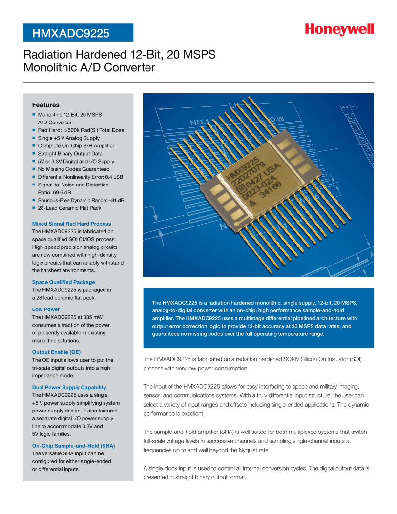
HMXADC9225
Radiation Hardened 12-Bit, 20 MSPS Monolithic A/D Converter
The HMXADC9225 is a radiation hardened monolithic, single supply, 12-bit, 20 MSPS,
analog-to-digital converter with an on-chip, high performance sample-and-hold
amplifier. The HMXADC9225 uses a multistage differential pipelined architecture with
output error correction logic to provide 12-bit accuracy at 20 MSPS data rates, and
guarantees no missing codes over the full operating temperature range.
Featuresn Monolithic 12-Bit, 20 MSPS
A/D Convertern Rad Hard: >500k Rad(Si) Total Dosen Single +5 V Analog Supplyn Complete On-Chip S/H Amplifier n Straight Binary Output Datan 5V or 3.3V Digital and I/O Supplyn No Missing Codes Guaranteedn Differential Nonlinearity Error: 0.4 LSBn Signal-to-Noise and Distortion
Ratio: 69.6 dBn Spurious-Free Dynamic Range: –81 dBn 28-Lead Ceramic Flat Pack
Mixed Signal Rad Hard Process
The HMXADC9225 is fabricated on
space qualified SOI CMOS process.
High-speed precision analog circuits
are now combined with high-density
logic circuits that can reliably withstand
the harshest environments.
Space Qualified Package
The HMXADC9225 is packaged in
a 28 lead ceramic flat pack.
Low Power
The HMXADC9225 at 335 mW
consumes a fraction of the power
of presently available in existing
monolithic solutions.
Output Enable (OE)
The OE input allows user to put the
tri-state digital outputs into a high
impedance mode.
Dual Power Supply Capability
The HMXADC9225 uses a single
+5 V power supply simplifying system
power supply design. It also features
a separate digital I/O power supply
line to accommodate 3.3V and
5V logic families.
On-Chip Sample-and-Hold (SHA)
The versatile SHA input can be
configured for either single-ended
or differential inputs.
The HMXADC9225 is fabricated on a radiation hardened SOI-IV Silicon On Insulator (SOI)
process with very low power consumption.
The input of the HMXADC9225 allows for easy interfacing to space and military imaging,
sensor, and communications systems. With a truly differential input structure, the user can
select a variety of input ranges and offsets including single-ended applications. The dynamic
performance is excellent.
The sample-and-hold amplifier (SHA) is well suited for both multiplexed systems that switch
full-scale voltage levels in successive channels and sampling single-channel inputs at
frequencies up to and well beyond the Nyquist rate.
A single clock input is used to control all internal conversion cycles. The digital output data is
presented in straight binary output format.
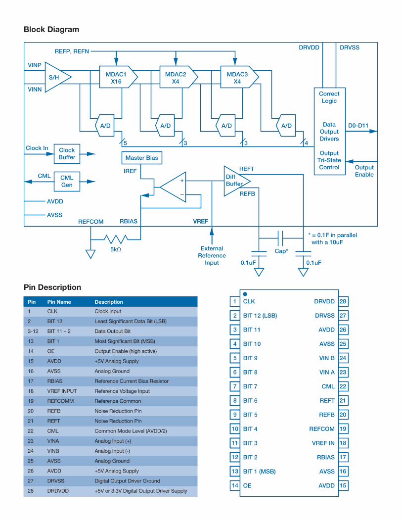
Pin Pin Name Description 1 CLK Clock Input
2 BIT 12 Least Significant Data Bit (LSB)
3-12 BIT 11 – 2 Data Output Bit
13 BIT 1 Most Significant Bit (MSB)
14 OE Output Enable (high active)
15 AVDD +5V Analog Supply
16 AVSS Analog Ground
17 RBIAS Reference Current Bias Resistor
18 VREF INPUT Reference Voltage Input
19 REFCOMM Reference Common
20 REFB Noise Reduction Pin
21 REFT Noise Reduction Pin
22 CML Common Mode Level (AVDD/2)
23 VINA Analog Input (+)
24 VINB Analog Input (-)
25 AVSS Analog Ground
26 AVDD +5V Analog Supply
27 DRVSS Digital Output Driver Ground
28 DRDVDD +5V or 3.3V Digital Output Driver Supply
Pin Description
Block Diagram
S/H MDAC1X16
MDAC2X4
MDAC3X4
A/D A/D A/D A/D
REFP, REFN
VINP
VINN
Clock In
CML
ClockBuffer
CMLGen
AVDD
AVSSREFCOM RBIAS VREFVREF
IREF
Master Bias
CorrectLogic
DataOutputDrivers
OutputTri-StateControl
DRVDD DRVSS
D0-D11
OutputEnable
REFT
REFB
ExternalReference
Input
5 3 3 4
+
–
DiffBuffer
Cap*
0.1uF 0.1uF
* = 0.1F in parallel with a 10uF
5kΩ
28
27
26
25
24
23
22
21
20
19
18
17
16
15
1
2
3
4
5
6
7
8
9
10
11
12
13
14
CLK
BIT 12 (LSB)
BIT 11
BIT 10
BIT 9
BIT 8
BIT 7
BIT 6
BIT 5
BIT 4
BIT 3
BIT 2
BIT 1 (MSB)
OE
DRVDD
DRVSS
AVDD
AVSS
VIN B
VIN A
CML
REFT
REFB
REFCOM
VREF IN
RBIAS
AVSS
AVDD
Signal Definition
DRVDD
The Digital Output Power Supply (DRVDD) can operate at either 5.0V
or 3.3V. The DRVDD voltage defines the interface voltage level for
all the digital I/O signals including Clock input, Output Enable, and all
data output signals.
Output Enable (OE)
This signal controls the electrical state of the digital output drivers.
A high logic level will enable the outputs and a low logic level will put
the output drivers into a high impedance state.
RBIAS
R-Bias is required to create the internal bias currents. An external
resistor with a value of 5kΩ shall be connected between pin 17 and
ground.
The R-Bias resistor can also be used to change the power
consumption. By changing the resistor value, the current
consumption can be changed. The range of this feature not yet
characterized.
Voltage Reference Input
The HMXADC9225 requires the user to provide an external voltage
reference as an INPUT to the device. The device is designed to
operate using a 1.0V to 2.0V external voltage reference. The input
range will then be defined by the VREF.
The full scale signal input = 2 x VREF. Signals outside this range will
be considered “out of range”.
CML (Common Mode Level)
This signal is an analog output at a value of AVDD/2. It can be used
as a reference for biasing external circuits to a “mid-rail” value. This
signal should be decoupled with a 0.1uF capacitor.
Total Ionizing Radiation Dose
The HMXADC9225 will meet all stated functional and electrical
specifications over the entire operating temperature range after
the specified total ionizing radiation dose. All electrical and timing
performance parameters will remain within specifications after
rebound at VDD = 5.0 V extrapolated to ten years of operation. Total
dose hardness is assured by wafer level testing of process monitor
transistors using 10 KeV X-ray and Co60 radiation sources. Transistor
gate threshold shift correlations have been made between 10 KeV
X-rays applied at a dose rate of 1x10⁵ rad(SiO2)/min at T=25°C and
gamma rays (Cobalt 60 source) to ensure that wafer level X-ray
testing is consistent with standard military radiation test environments.
Transient Pulse Ionizing Radiation
The HMXADC9225 will meet any functional or electrical specification
after exposure to a radiation pulse up to the transient dose rate
survivability specification, when applied under recommended
operating conditions. Note that the current conducted during the
pulse by the ADC inputs, outputs, and power supply may significantly
exceed the normal operating levels. The application design must
accommodate these effects.
Soft Error Rate
The HMXADC9225 is not guaranteed to operate through an SEU
or dose rate event, but it will recover and continue to meet all
specifications over the full temperature range after an event.
Latchup and Snapback
The HMXADC9225 will not latch up due to any of the above radiation
exposure conditions when applied under recommended operating
conditions. Fabrication with the SIMOX substrate material provides
oxide isolation between adjacent PMOS and NMOS transistors and
eliminates any potential SCR latchup structures. Sufficient transistor
body tie connections to the p- and n-channel substrates are made to
ensure no source/drain snapback occurs.
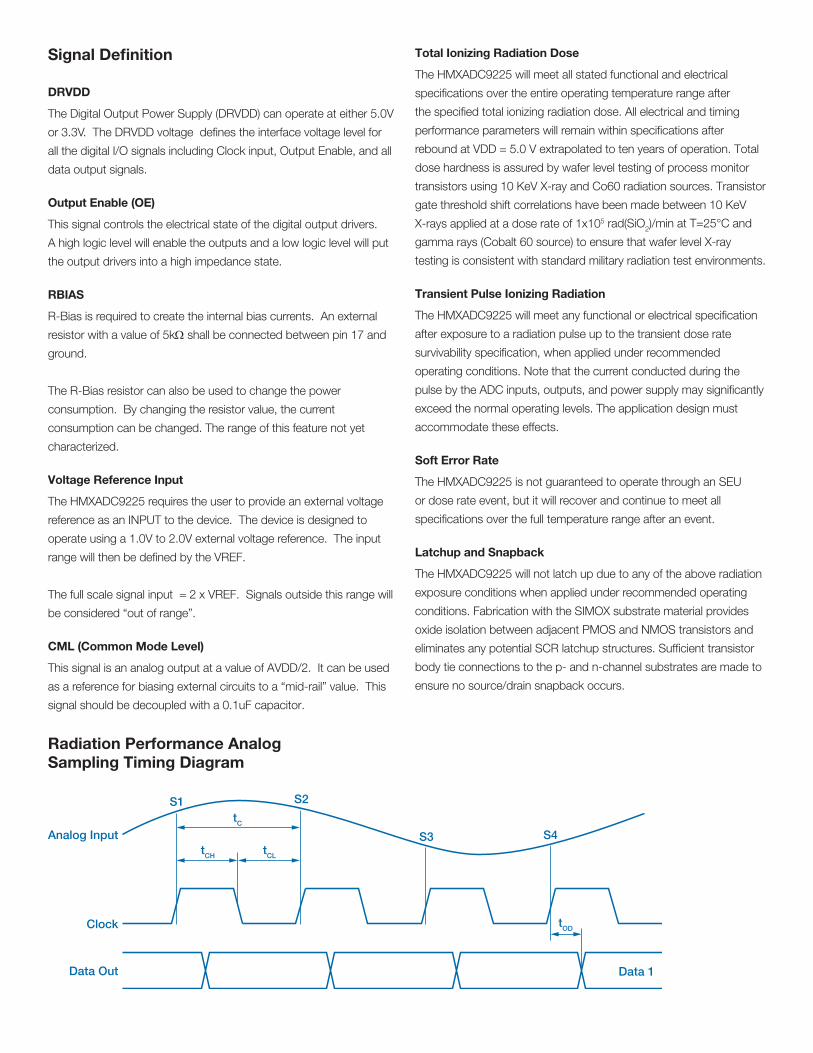
Radiation Performance Analog Sampling Timing Diagram
S1 S2
S3 S4tC
tCH tCL
tOD
Data 1
Analog Input
Clock
Data Out
Parameters Min Max Units Total Dose Hardness >5 x 10⁵ Rad (Si)
Dose Rate Upset Hardness >2.5 x 10¹² Rad(Si)/sec
Dose Rate Survivability >2.5 x 10¹² Rad(Si)/sec
Soft Error Rate LET (1) 120 MeV cm2/mg
Soft Error Rate (2) <1x10⁻¹⁰ Upsets/bit-day
Latch Up Immune
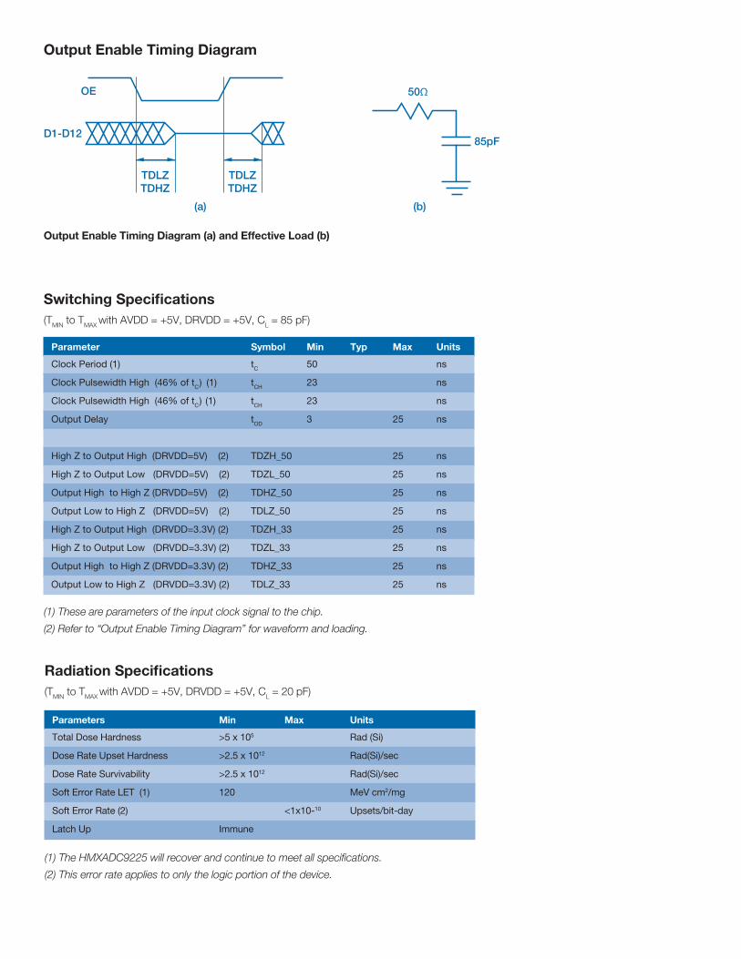
Output Enable Timing Diagram
Switching Specifications(TMIN to TMAX with AVDD = +5V, DRVDD = +5V, CL = 85 pF)
Parameter Symbol Min Typ Max Units Clock Period (1) tC 50 ns
Clock Pulsewidth High (46% of tC) (1) tCH 23 ns
Clock Pulsewidth High (46% of tC) (1) tCH 23 ns
Output Delay tOD 3 25 ns
High Z to Output High (DRVDD=5V) (2) TDZH_50 25 ns
High Z to Output Low (DRVDD=5V) (2) TDZL_50 25 ns
Output High to High Z (DRVDD=5V) (2) TDHZ_50 25 ns
Output Low to High Z (DRVDD=5V) (2) TDLZ_50 25 ns
High Z to Output High (DRVDD=3.3V) (2) TDZH_33 25 ns
High Z to Output Low (DRVDD=3.3V) (2) TDZL_33 25 ns
Output High to High Z (DRVDD=3.3V) (2) TDHZ_33 25 ns
Output Low to High Z (DRVDD=3.3V) (2) TDLZ_33 25 ns
Radiation Specifications(TMIN to TMAX with AVDD = +5V, DRVDD = +5V, CL = 20 pF)
(1) These are parameters of the input clock signal to the chip.
(2) Refer to “Output Enable Timing Diagram” for waveform and loading.
(1) The HMXADC9225 will recover and continue to meet all specifications.
(2) This error rate applies to only the logic portion of the device.
OE 50Ω
D1-D12
TDLZTDHZ
TDLZTDHZ
85pF
(a) (b)
Output Enable Timing Diagram (a) and Effective Load (b)
Absolute Maximum Ratings(AVDD = +5V, DRVDD = +5V, unless otherwise noted)
Parameters Min Max Units AVDD 6.5 Volts
DRVDD 6.5 Volts
AVSS -0.3 Volts
DRVSS -0.3 Volts
REFGND -0.3 Volts
CLK, OE 6.5 Volts
D1-D12 6.5 Volts
VINA, VINB 6.5 Volts
VREF 6.5 Volts
REFT, REFB 6.5 Volts
Package Thermal Resistance (θJC) 2.0 °C/W
Junction Temperature +175 °C
(1) All voltages are with respect to VSS = 0V.
Parameters Min Type Max Units AVDD 4.75 5 5.25 Volts
DRVDD (for 5V I/O operation) 4.75 5 5.25 Volts
DRVDD (for 3.3V I/O operation) 3.0 3.3 3.6 Volts
AVSS -0.3 0 Volts
DRVSS -0.3 0 Volts
REFGND -0.3 0 Volts
CLK, OE DRVDD + 0.5 Volts
D1-D12 5.5 Volts
VINA, VINB 0.5 4.5 Volts
VREF 1.0 2.0 Volts
REFT, REFB 5.5 Volts
Operating Temperature (case) -55 +125 °C
Recommended Operating Conditions
(1) All voltages are with respect to VSS = 0V.
ESD (Electrostatic Discharge) SensitiveThe HMXADC9225 is rated as Class 1B ESD. Proper ESD precautions should be taken to
avoid degradation or damage to the device.
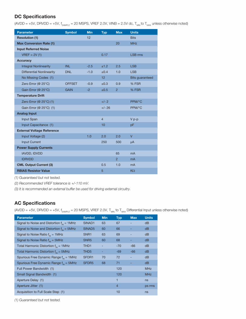
DC Specifications(AVDD = +5V, DRVDD = +5V, fSAMPLE = 20 MSPS, VREF 2.0V, VINB = 2.5V dc, TMIN to TMAX unless otherwise noted)
Parameter Symbol Min Typ Max Units Resolution (1) 12 Bits Max Conversion Rate (1) 20 MHz Input Referred Noise VREF = 2V (1) 0.17 LSB rms Accuracy Integral Nonlinearity INL -2.5 ±1.2 2.5 LSB Differential Nonlinearity DNL -1.0 ±0.4 1.0 LSB No Missing Codes (1) 12 Bits guaranteed
Zero Error (@ 25°C) OFFSET -0.9 ±0.3 0.9 % FSR
Gain Error (@ 25°C) GAIN -2 ±0.5 2 % FSR Temperature Drift
Zero Error (@ 25°C) (1) +/- 2 PPM/°C
Gain Error (@ 25°C) (1) +/- 26 PPM/°C Analog Input Input Span 4 V p-p Input Capacitance (1) 10 pF External Voltage Reference Input Voltage (2) 1.0 2.0 2.0 V Input Current 250 500 μA Power Supply Currents IAVDD, IDVDD 65 mA
IDRVDD 2 mA CML Output Current (3) 0.5 1.0 mA
RBIAS Resistor Value 5 KΩ
(1) Guaranteed but not tested.
(2) Recommended VREF tolerance is +/-110 mV.
(3) It is recommended an external buffer be used for driving external circuitry.
Parameter Symbol Min Typ Max Units Signal to Noise and Distortion fIN = 1MHz SINAD1 63 67 - dB Signal to Noise and Distortion fIN = 5MHz SINAD5 60 66 - dB Signal to Noise Ratio fIN = 1MHz SNR1 63 69 - dB Signal to Noise Ratio fIN = 5MHz SNR5 60 68 - dB Total Harmonic Distortion fIN = 1MHz THD1 - -70 -66 dB Total Harmonic Distortion fIN = 5MHz THD5 - -69 -66 dB Spurious Free Dynamic Range fIN = 1MHz SFDR1 70 72 - dB Spurious Free Dynamic Range fIN = 5MHz SFDR5 68 71 - dB Full Power Bandwidth (1) 120 MHz Small Signal Bandwidth (1) 120 MHz Aperture Delay (1) 1 ns Aperture Jitter (1) 4 ps rms
Acquisition to Full Scale Step (1) 10 ns
AC Specifications(AVDD = +5V, DRVDD = +5V, fSAMPLE = 20 MSPS, VREF 2.0V, TMIN to TMAX Differential Input unless otherwise noted)
(1) Guaranteed but not tested.
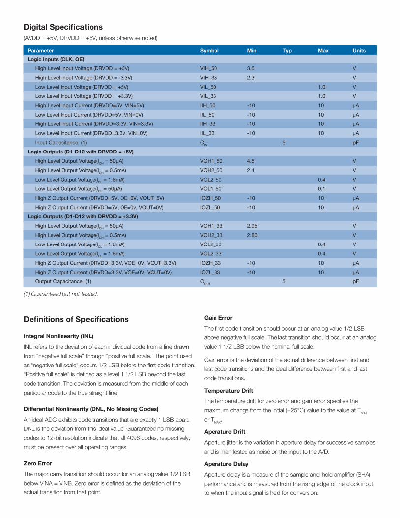
Digital Specifications(AVDD = +5V, DRVDD = +5V, unless otherwise noted)
Parameter Symbol Min Typ Max Units Logic Inputs (CLK, OE) High Level Input Voltage (DRVDD = +5V) VIH_50 3.5 V High Level Input Voltage (DRVDD =+3.3V) VIH_33 2.3 V Low Level Input Voltage (DRVDD = +5V) VIL_50 1.0 V Low Level Input Voltage (DRVDD = +3.3V) VIL_33 1.0 V High Level Input Current (DRVDD=5V, VIN=5V) IIH_50 -10 10 μA Low Level Input Current (DRVDD=5V, VIN=0V) IIL_50 -10 10 μA High Level Input Current (DRVDD=3.3V, VIN=3.3V) IIH_33 -10 10 μA Low Level Input Current (DRVDD=3.3V, VIN=0V) IIL_33 -10 10 μA Input Capacitance (1) CIN 5 pF
Logic Outputs (D1-D12 with DRVDD = +5V) High Level Output Voltage(IOH = 50μA) VOH1_50 4.5 V High Level Output Voltage(IOH = 0.5mA) VOH2_50 2.4 V Low Level Output Voltage(IOL = 1.6mA) VOL2_50 0.4 V Low Level Output Voltage(IOL = 50μA) VOL1_50 0.1 V High Z Output Current (DRVDD=5V, OE=0V, VOUT=5V) IOZH_50 -10 10 μA High Z Output Current (DRVDD=5V, OE=0v, VOUT=0V) IOZL_50 -10 10 μA Logic Outputs (D1-D12 with DRVDD = +3.3V) High Level Output Voltage(IOH = 50μA) VOH1_33 2.95 V High Level Output Voltage(IOH = 0.5mA) VOH2_33 2.80 V Low Level Output Voltage(IOL = 1.6mA) VOL2_33 0.4 V Low Level Output Voltage(IOL = 1.6mA) VOL2_33 0.4 V High Z Output Current (DRVDD=3.3V, VOE=0V, VOUT=3.3V) IOZH_33 -10 10 μA High Z Output Current (DRVDD=3.3V, VOE=0V, VOUT=0V) IOZL_33 -10 10 μA Output Capacitance (1) COUT 5 pF
(1) Guaranteed but not tested.
Definitions of Specifications
Integral Nonlinearity (INL)
INL refers to the deviation of each individual code from a line drawn
from “negative full scale” through “positive full scale.” The point used
as “negative full scale” occurs 1/2 LSB before the first code transition.
“Positive full scale” is defined as a level 1 1/2 LSB beyond the last
code transition. The deviation is measured from the middle of each
particular code to the true straight line.
Differential Nonlinearity (DNL, No Missing Codes)
An ideal ADC exhibits code transitions that are exactly 1 LSB apart.
DNL is the deviation from this ideal value. Guaranteed no missing
codes to 12-bit resolution indicate that all 4096 codes, respectively,
must be present over all operating ranges.
Zero Error
The major carry transition should occur for an analog value 1/2 LSB
below VINA = VINB. Zero error is defined as the deviation of the
actual transition from that point.
Gain Error
The first code transition should occur at an analog value 1/2 LSB
above negative full scale. The last transition should occur at an analog
value 1 1/2 LSB below the nominal full scale.
Gain error is the deviation of the actual difference between first and
last code transitions and the ideal difference between first and last
code transitions.
Temperature Drift
The temperature drift for zero error and gain error specifies the
maximum change from the initial (+25°C) value to the value at TMIN
or TMAX.
Aperature Drift
Aperture jitter is the variation in aperture delay for successive samples
and is manifested as noise on the input to the A/D.
Aperature Delay
Aperture delay is a measure of the sample-and-hold amplifier (SHA)
performance and is measured from the rising edge of the clock input
to when the input signal is held for conversion.
Signal-to-Noise and Distortion (S/N+D, SINAD) Ratio
S/N+D is the ratio of the rms value of the measured input signal to
the rms sum of all other spectral components below the Nyquist
frequency, including harmonics but excluding dc. The value for S/
N+D is expressed in decibels.
Effective Number of Bits (ENOB)
For a sine wave, SINAD can be expressed in terms of the number of
bits. Using the following formula,
N = (SINAD – 1.76)/6.02
it is possible to get a measure of performance expressed as N, the
effective number of bits. Thus, effective number of bits for a device for
sine wave inputs at a given input frequency can be calculated directly
from its measured SINAD.
Total Harmonic Distortion (THD)
THD is the ratio of the rms sum of the first six harmonic components
to the rms value of the measured input signal and is expressed as a
percentage or in decibels.
Signal-to-Noise Ratio (SNR)
SNR is the ratio of the rms value of the measured input signal to
the rms sum of all other spectral components below the Nyquist
frequency, excluding the first six harmonics and dc. The value for
SNR is expressed in decibels.
Spurious Free Dynamic Range (SFDR)
SFDR is the difference in dB between the rms amplitude of the input
signal and the peak spurious signal.
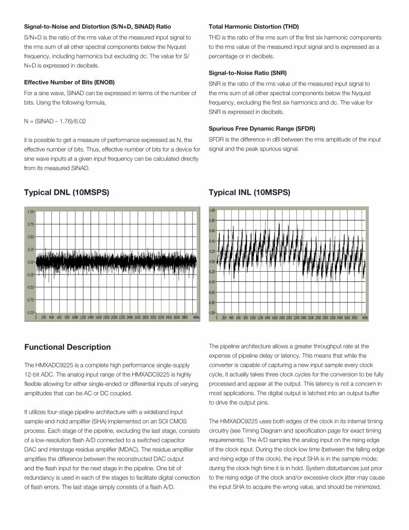
Typical DNL (10MSPS) Typical INL (10MSPS)
Functional Description
The HMXADC9225 is a complete high performance single-supply
12-bit ADC. The analog input range of the HMXADC9225 is highly
flexible allowing for either single-ended or differential inputs of varying
amplitudes that can be AC or DC coupled.
It utilizes four-stage pipeline architecture with a wideband input
sample-and-hold amplifier (SHA) implemented on an SOI CMOS
process. Each stage of the pipeline, excluding the last stage, consists
of a low-resolution flash A/D connected to a switched capacitor
DAC and interstage residue amplifier (MDAC). The residue amplifier
amplifies the difference between the reconstructed DAC output
and the flash input for the next stage in the pipeline. One bit of
redundancy is used in each of the stages to facilitate digital correction
of flash errors. The last stage simply consists of a flash A/D.
The pipeline architecture allows a greater throughput rate at the
expense of pipeline delay or latency. This means that while the
converter is capable of capturing a new input sample every clock
cycle, it actually takes three clock cycles for the conversion to be fully
processed and appear at the output. This latency is not a concern in
most applications. The digital output is latched into an output buffer
to drive the output pins.
The HMXADC9225 uses both edges of the clock in its internal timing
circuitry (see Timing Diagram and specification page for exact timing
requirements). The A/D samples the analog input on the rising edge
of the clock input. During the clock low time (between the falling edge
and rising edge of the clock), the input SHA is in the sample mode;
during the clock high time it is in hold. System disturbances just prior
to the rising edge of the clock and/or excessive clock jitter may cause
the input SHA to acquire the wrong value, and should be minimized.
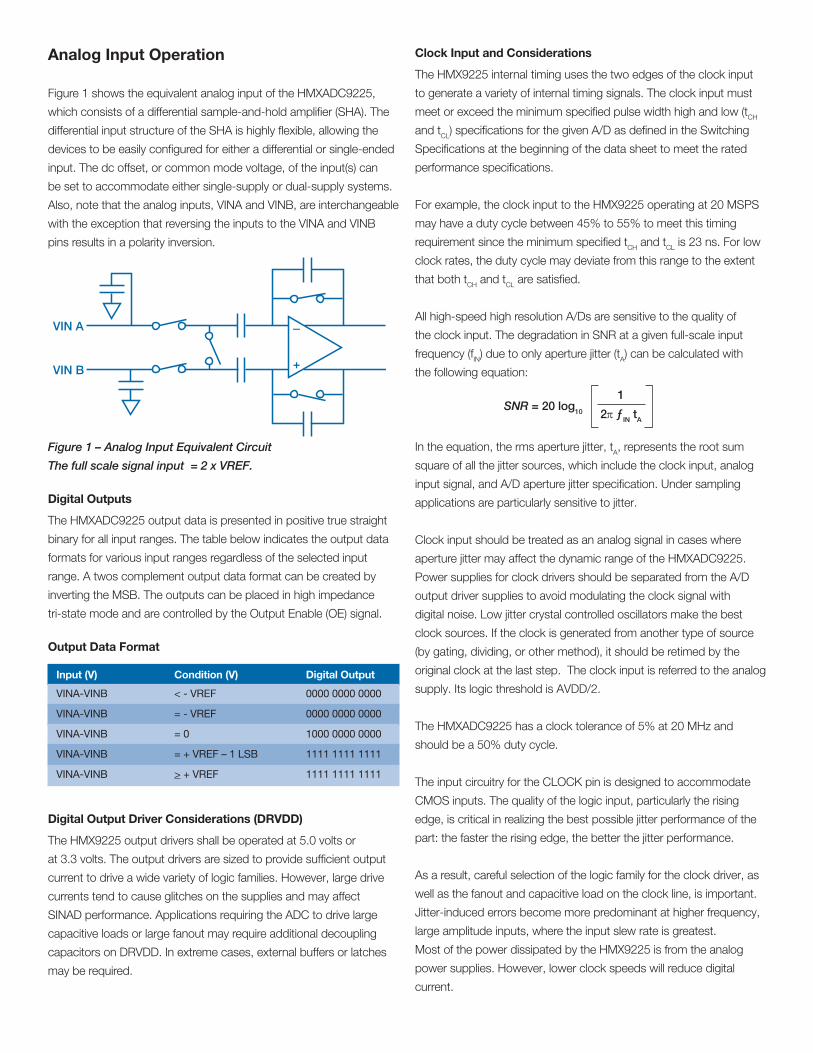
Analog Input Operation
Figure 1 shows the equivalent analog input of the HMXADC9225,
which consists of a differential sample-and-hold amplifier (SHA). The
differential input structure of the SHA is highly flexible, allowing the
devices to be easily configured for either a differential or single-ended
input. The dc offset, or common mode voltage, of the input(s) can
be set to accommodate either single-supply or dual-supply systems.
Also, note that the analog inputs, VINA and VINB, are interchangeable
with the exception that reversing the inputs to the VINA and VINB
pins results in a polarity inversion.
Figure 1 – Analog Input Equivalent Circuit
The full scale signal input = 2 x VREF.
Digital Outputs
The HMXADC9225 output data is presented in positive true straight
binary for all input ranges. The table below indicates the output data
formats for various input ranges regardless of the selected input
range. A twos complement output data format can be created by
inverting the MSB. The outputs can be placed in high impedance
tri-state mode and are controlled by the Output Enable (OE) signal.
Output Data Format
Clock Input and Considerations
The HMX9225 internal timing uses the two edges of the clock input
to generate a variety of internal timing signals. The clock input must
meet or exceed the minimum specified pulse width high and low (tCH
and tCL) specifications for the given A/D as defined in the Switching
Specifications at the beginning of the data sheet to meet the rated
performance specifications.
For example, the clock input to the HMX9225 operating at 20 MSPS
may have a duty cycle between 45% to 55% to meet this timing
requirement since the minimum specified tCH and tCL is 23 ns. For low
clock rates, the duty cycle may deviate from this range to the extent
that both tCH and tCL are satisfied.
All high-speed high resolution A/Ds are sensitive to the quality of
the clock input. The degradation in SNR at a given full-scale input
frequency (fIN) due to only aperture jitter (tA) can be calculated with
the following equation:
In the equation, the rms aperture jitter, tA, represents the root sum
square of all the jitter sources, which include the clock input, analog
input signal, and A/D aperture jitter specification. Under sampling
applications are particularly sensitive to jitter.
Clock input should be treated as an analog signal in cases where
aperture jitter may affect the dynamic range of the HMXADC9225.
Power supplies for clock drivers should be separated from the A/D
output driver supplies to avoid modulating the clock signal with
digital noise. Low jitter crystal controlled oscillators make the best
clock sources. If the clock is generated from another type of source
(by gating, dividing, or other method), it should be retimed by the
original clock at the last step. The clock input is referred to the analog
supply. Its logic threshold is AVDD/2.
The HMXADC9225 has a clock tolerance of 5% at 20 MHz and
should be a 50% duty cycle.
The input circuitry for the CLOCK pin is designed to accommodate
CMOS inputs. The quality of the logic input, particularly the rising
edge, is critical in realizing the best possible jitter performance of the
part: the faster the rising edge, the better the jitter performance.
As a result, careful selection of the logic family for the clock driver, as
well as the fanout and capacitive load on the clock line, is important.
Jitter-induced errors become more predominant at higher frequency,
large amplitude inputs, where the input slew rate is greatest.
Most of the power dissipated by the HMX9225 is from the analog
power supplies. However, lower clock speeds will reduce digital
current.
Input (V) Condition (V) Digital Output VINA-VINB < - VREF 0000 0000 0000
VINA-VINB = - VREF 0000 0000 0000
VINA-VINB = 0 1000 0000 0000
VINA-VINB = + VREF – 1 LSB 1111 1111 1111
VINA-VINB > + VREF 1111 1111 1111
Digital Output Driver Considerations (DRVDD)
The HMX9225 output drivers shall be operated at 5.0 volts or
at 3.3 volts. The output drivers are sized to provide sufficient output
current to drive a wide variety of logic families. However, large drive
currents tend to cause glitches on the supplies and may affect
SINAD performance. Applications requiring the ADC to drive large
capacitive loads or large fanout may require additional decoupling
capacitors on DRVDD. In extreme cases, external buffers or latches
may be required.
VIN A
VIN B
+
–
SNR = 20 log10
1
2p ƒIN tA
Grounding and Decoupling
Analog and Digital Grounding
Proper grounding is essential in any high speed, high-resolution
system. Multilayer printed circuit boards (PCBs) are recommended to
provide optimal grounding and power schemes. The use of ground
and power planes offers distinct advantages:
1. The minimization of the loop area encompassed by a signal
and its return path.
2. The minimization of the impedance associated with ground
and power paths.
3. The inherent distributed capacitor formed by the power plane,
PCB insulation and ground plane.
These characteristics result in both a reduction of electromagnetic
interference (EMI) and an overall improvement in performance.
It is important to design a layout that prevents noise from coupling
onto the input signal. Digital signals should not be run in parallel
with input signal traces and should be routed away from the input
circuitry. While the HMXADC9225 features separate analog and
driver ground pins, it should be treated as an analog component.
The AVSS and DRVSS pins must be joined together directly under
the HMXADC9225. A solid ground plane under the A/D is acceptable
if the power and ground return currents are carefully managed.
Alternatively, the ground plane under the A/D may contain serrations
to steer currents in predictable directions where cross coupling
between analog and digital would otherwise be unavoidable.
Analog and Digital Driver Supply Decoupling
The HMXADC9225 features separate analog and driver supply
and ground pins, helping to minimize digital corruption of sensitive
analog signals.
In general, AVDD, the analog supply, should be decoupled to AVSS,
the analog common, as close to the chip as physically possible.
It is recommended to use 0.1 uF ceramic chip and 10 uF tantalum
capacitors for the AVDD and DRVDD power inputs. A 0.1 uF ceramic
chip capacitor is adequate on the CML pin.
Quality and Radiation Hardness Assurance
Honeywell maintains a high level of product integrity through process
control, utilizing statistical process and six sigma controls. It is part of
a “Total Quality Assurance Program”, the computer based process
performance tracking system and a radiation hardness assurance
strategy.
Screening Levels
Honeywell offers several levels of device screening to meet your
needs. “Engineering Devices” are available with limited performance
and screening for prototype development and evaluation testing.
Hi-Rel Level B based and S based devices undergo additional
screening per the requirements of MIL-STD-883.
Reliability
Honeywell understands the stringent reliability requirements that
space and defense systems requires and has extensive experience
in reliability testing on programs of this nature. Reliability attributes
of the SOI process were characterized by testing specially designed
structures to evaluate failure mechanisms including hot carriers,
electro-migration, and time-dependent dielectric breakdown. The
results are fed back to improve the process to ensure the highest
reliability products.
In addition, our products are subjected to dynamic, accelerated life
tests. The packages used are qualified through MIL-STD-883,
TM 5005 Class S. The product screening flow can be modified to
meet the customer’s specific requirements. Quality conformance
testing is performed as an option on all production lots to ensure
on-going reliability.
D1
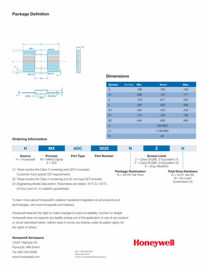
E2E1
L1
e
bNO.14 NO.15
NO.1 NO.28
(.300)(0.55) .026 MIN
A1
c
A
Honeywell Aerospace
12001 Highway 55
Plymouth, MN 55441
Tel: 800-323-8295
www.honeywell.com
N61-1063-000-000December 2010© 2010 Honeywell International Inc.
To learn more about Honeywell’s radiation hardened integrated circuit products and
technologies, visit www.honeywell.com/radhard.
Honeywell reserves the right to make changes to improve reliability, function or design.
Honeywell does not assume any liability arising out of the application or use of any product
or circuit described herein; neither does it convey any license under its patent rights nor
the rights of others.
Ordering Information
ProcessM = Mixed Signal
X = SOI
Screen LevelZ = Class S\QML V Equivalent (1)Y = Class B\QML Q Equivalent (2)
E = Eng. Model(3)
SourceH = Honeywell
Part Number
Package DestinationN = 28 Pin Flat Pack
Part Type
NAND00
H MX ADC 9225 N Z H
Total Dose HardnessG = 5x10⁵ rad (Si)
N = No Level Guaranteed (3)
(1) These receive the Class V screening and QCI is included.
Customer must specify QCI requirements.
(2) These receive the Class V screening but do not have QCI included.
(3) Engineering Model Description: Parameters are tested -55°C to 125°C,
24 hour burn-in, no radiation guaranteed
Package Definition
Dimensions
Symbol (Inches) Min. Norm Max. A .108 .120 .133
A1 .098 .107 .117
b .015 .017 .019
c .004 .005 .006
D1 .404 .410 .416
E1 .712 .720 .728
E2 .645 .650 .655
e .050 BSC
L1 1.150 BSC
N 28