Embed Size (px)
Citation preview

Holographically formed three-dimensional Penrose-type photonic quasicrystal through a
lab-made single diffractive optical element
Ahmad Harb,1,2
Faraon Torres,1,2
Kris Ohlinger,1,2
Yuankun Lin,1,4*
Karen Lozano,2
Di Xu,3 and Kevin P. Chen
3
1Department of Physics and Geology, University of Texas-Pan American, Edinburg, Texas 78541, USA 2Department of Mechanical Engineering, University of Texas-Pan American, Edinburg, Texas 78541, USA
3Department of Electrical and Computer Engineering, University of Pittsburgh, Pittsburgh, PA 15261, USA 4Current address: Department of Physics, University of North Texas, Denton, Texas 76203, USA
Abstract: Large-area three-dimensional Penrose-type photonic quasicrystals are fabricated through a holographic lithography method using a lab-made diffractive optical element and a single laser exposure. The diffractive optical element consists of five polymer gratings symmetrically orientated around a central opening. The fabricated Penrose-type photonic quasicrystal shows ten-fold rotational symmetry. The Laue diffraction pattern from the photonic quasi-crystal is observed to be similar to that of the traditional alloy quasi-crystal. A golden ratio of 1.618 is also observed for the radii of diffraction rings, which has not been observed before in artificial photonic quasicrystals.
© 2010 Optical Society of American
OCIS codes: (260.3160) Interference; (050.1970) Diffractive optics; (220.4000) Microstructure fabrication; (090.0090) Holography.
References and links
1. E. Yablonovitch, “Inhibited spontaneous emission in solid-state physics and electronics,” Phys. Rev. Lett. 58(20), 2059–2062 (1987).
2. S. John, “Strong localization of photons in certain disordered dielectric superlattices,” Phys. Rev. Lett. 58(23), 2486–2489 (1987).
3. M. E. Zoorob, M. D. B. Charlton, G. J. Parker, J. J. Baumberg, and M. C. Netti, “Complete photonic bandgaps in 12-fold symmetric quasicrystals,” Nature 404(6779), 740–743 (2000).
4. W. Man, M. Megens, P. J. Steinhardt, and P. M. Chaikin, “Experimental measurement of the photonic properties of icosahedral quasicrystals,” Nature 436(7053), 993–996 (2005).
5. S. Y. Lin, J. G. Fleming, D. L. Hetherington, B. K. Smith, R. Biswas, K. M. Ho, M. M. Sigalas, W. Zubrzycki, S. R. Kurtz, and J. Bur, “Three-dimensional photonic crystal operating at infrared wavelengths,” Nature 394(6690), 251–253 (1998).
6. J. E. G. J. Wijnhoven, and W. L. Vos, “Preparation of photonic crystals made of air spheres in titania,” Science 281(5378), 802–804 (1998).
7. M. Deubel, G. von Freymann, M. Wegener, S. Pereira, K. Busch, and C. M. Soukoulis, “Direct laser writing of three-dimensional photonic-crystal templates for telecommunications,” Nat. Mater. 3(7), 444–447 (2004).
8. M. Campbell, D. N. Sharp, M. T. Harrison, R. G. Denning, and A. J. Turberfield, “Fabrication of photonic crystals for the visible spectrum by holographic lithography,” Nature 404(6773), 53–56 (2000).
9. A. Ledermann, L. Cademartiri, M. Hermatschweiler, C. Toninelli, G. A. Ozin, D. S. Wiersma, M. Wegener, and G. von Freymann, “Three-dimensional silicon inverse photonic quasicrystals for infrared wavelengths,” Nat. Mater. 5(12), 942–945 (2006).
10. S. P. Gorkhali, J. Qi, and G. P. Grawford, “Electrically switchable mesoscale Penrose quasicrystal structure,” Appl. Phys. Lett. 86(1), 011110 (2005).
11. X. Wang, C. Y. Ng, W. Y. Tam, C. T. Chan, and P. Sheng, “Large-area two-dimensional mesoscale quasi-crystals,” Adv. Mater. 15(18), 1526–1528 (2003).
12. X. Wang, J. Xu, J. C. W. Lee, Y. K. Pang, W. Y. Tam, C. T. Chan, and P. Sheng, “Realization of optical periodic quasicrystals using holographic lithography,” Appl. Phys. Lett. 88(5), 051901 (2006).
13. W. Y. Tam, “Icosahedral quasicrystals by optical interference holography,” Appl. Phys. Lett. 89(25), 251111 (2006).
14. J. Xu, R. Ma, X. Wang, and W. Y. Tam, “Icosahedral quasicrystals for visible wavelengths by optical interference holography,” Opt. Express 15(7), 4287–4295 (2007), http://www.opticsinfobase.org/oe/abstract.cfm?URI=oe-15-7-4287.
#132195 - $15.00 USD Received 26 Jul 2010; revised 29 Aug 2010; accepted 30 Aug 2010; published 10 Sep 2010(C) 2010 OSA 13 September 2010 / Vol. 18, No. 19 / OPTICS EXPRESS 20512

15. Y. Lin, P. R. Herman, and K. Darmawikarta, “Design and holographic fabrication of tetragonal and cubic photonic crystals with phase mask: toward the mass-production of three-dimensional photonic crystals,” Appl. Phys. Lett. 86, 071117/1–3 (2005).
16. Y. Lin, A. Harb, D. Rodriguez, K. Lozano, D. Xu, and K. P. Chen, “Fabrication of two-layer integrated phase mask for single-beam and single-exposure fabrication of three-dimensional photonic crystal,” Opt. Express 16(12), 9165–9172 (2008), http://www.opticsinfobase.org/oe/abstract.cfm?URI=oe-16-12-9165.
17. N. Tereault, G. von Freymann, M. Deubel, M. Hermatschweiler, F. Perez-Willard, S. John, M. Wegener, and G. A. Ozin, “New route to three-dimensional photonic bandgap materials: silicon double inversion of polymer templates,” Adv. Mater. 18(4), 457–460 (2006).
18. D. Shechtman, I. Blech, D. Gratias, and J. W. Cahn, “Metallic phase with long range orientataional order and no translational symmetry,” Phys. Rev. Lett. 53(20), 1951–1953 (1984).
19. D. Levine, and P. J. Steinhardt, “Quasicrystal: a new class of ordered structures,” Phys. Rev. Lett. 53(26), 2477–2480 (1984).
1. Introduction
Photonic crystals have been intensively studied due to the existence of photonic bandgaps in the crystal. Their periodically varying refractive indices can prevent the propagation of electromagnetic waves with certain wavelengths [1,2]. The anisotropy of a photonic bandgap depends on the symmetry of the photonic crystal lattice. With high lattice symmetries, the first Brillouin zone becomes more circular and the stop-band in all directions overlaps to form a complete photonic bandgap [3,4]. In traditional photonic crystals, two-, three-, four- and six-fold rotational symmetries are allowed, however, five-, seven- and higher-fold rotational symmetries are forbidden. It has been shown that photonic quasi-periodic crystals (or called quasi-crystals) have higher rotational symmetries (five, seven, and all high-fold symmetry) and thus more isotropic bandgaps leading to more interesting wave propagation properties than traditional photonic crystals [3,4]. It has been demonstrated experimentally that a complete photonic bandgap can be realized in quasi-periodic lattices of small air holes in materials of low refractive index such as silicon nitride and even glass. This property can enable coupling of light from quasi-crystal device to optical fiber with low optical coupling loss [3].
In the last decade, several elegant techniques have succeeded in fabricating three-dimensional (3D) photonic crystals, such as conventional multilayer stacking of woodpile structures using semiconductor fabrication processes [5], colloidal self-assembly [6], multi-photon direct laser writing [7], and holographic lithography [8]. However, some traditional fabrication techniques, such as self-assembly of microspheres and layer-by-layer fabrication, are prohibitive for the fabrication of photonic quasi-crystals. Multi-photon lithography and stereolithography have demonstrated capabilities in the fabrication of 3D icosahedral quasicrystal but are limited by the large processing time required [4,9]. Holographic lithography has been very successful in fabricating photonic crystal templates through multi-beam interference controlled by the number of interfering laser beams, their interfering angle and relative phases [8]. Holographic lithography has also been used for the fabrication of photonic quasi-crystals [10–14]. 3D icosahedral photonic quasicrystals are formed via seven-beam interference with five beams five-fold-symmetrically surrounding two oppositely-propagating beams [13,14]. The single optical element (such as prism [14] or phase mask [15,16]) based holographic lithography has greatly reduced the optics setup complexity and improved the mechanical stability for the micro/nano-fabrication of photonic structures. Through the holographic lithography, the interference pattern is usually recorded in a photo-sensitive resist which has a low index of refraction. The photonic quasicrystal template in polymer can be converted into high refractive index materials such as silicon to have a photonic band gap in crystal. The template can be infiltrated at room temperature with SiO2 and burned away, leaving behind a daughter “inverse” template [17]. Then, the daughter template is inverted by infiltration with silicon and selective etching of the SiO2 [17].
In this paper, we demonstrate the laser holographic fabrication of 3D Penrose-type photonic quasicrystal templates using a lab-made diffractive optical element (DOE) with five gratings orientated five-fold symmetrically. The adaptation of a single DOE to holographic lithography drastically reduces the fabrication complexity. The Laue diffraction pattern from
#132195 - $15.00 USD Received 26 Jul 2010; revised 29 Aug 2010; accepted 30 Aug 2010; published 10 Sep 2010(C) 2010 OSA 13 September 2010 / Vol. 18, No. 19 / OPTICS EXPRESS 20513

the fabricated photonic crystal shows a pentagon-shaped ghost-face like pattern and a golden ratio of 1.618, which have not been observed before in 3D artificial photonic quasi-crystals.
Fig. 1. (a) The scheme for the lab fabricated diffractive optical element. Each of the five oriented gratings has the structure as imaged by AFM in (b) with a periodicity of 0.781 μm as measured by the section analysis (c).
Fig. 2. (a) Laser experimental setup for the holographic lithography; (b) Enlarged view of the lab-made DOE and beam propagation for generating the six-beam interference for the holographic fabrication of photonic quasi-crystals.
2. Lab-made diffractive optical element and theoretic description of holography
Figure 1(a) shows a scheme of a single DOE consisting of five gratings produced by recording gratings in a photosensitive mixture. A low power laser (Coherent Compass, 532 nm, 60 mW) was used in order to control the exposure condition and thus to obtain high diffraction efficiency. The laser beam was expanded to a size of 5 mm and separated into two by using a 50:50 beam splitter. Two laser beams overlap and form grating in the mixture. The photoresist mixture consists of dipentaerythritol penta/hexaacrylate monomer (88.5%), photo initiator rose bengal (0.2%), co-initiator N-phenyl glycine (0.8%) and chain extender N-vinyl pyrrolidinone (10.5%). The mixture was spin-coated on a microscope glass slide with a speed of 3000 rpm for 2 minutes to produce a thin film. The glass slide was mounted on a rotation stage. The rotation stage was mounted such that the overlapped beams that make up the exposure spot were 5 mm away from the rotation center. The glass slide was rotated by 72 degrees for each successive exposure until a total five gratings were produced. The exposure time was 2 seconds for each exposure. After exposure, the photoresist mixture was developed directly in propylene glycol methyl ether acetate (PGMEA) for 20 s, followed by rinsing in isopropanol for 10 s and air drying. The size of single fabricated grating is approximately 5 mm in diameter and the grating shows uniform colors under a white light.
Figure 1(b) shows Atomic Force Microscope (AFM) of the fabricated grating in the thin polymer. Figure 1(c) shows the section analysis of the measured AFM topography. From the Figs. 1(b) and 1(c), the period of the grating is measured to be 0.781 μm. Thus the fabricated DOE consists of the central opening surrounded by five diffraction gratings orientated five-
#132195 - $15.00 USD Received 26 Jul 2010; revised 29 Aug 2010; accepted 30 Aug 2010; published 10 Sep 2010(C) 2010 OSA 13 September 2010 / Vol. 18, No. 19 / OPTICS EXPRESS 20514

fold symmetrically. The DOE is mounted in the expanded laser beam and five beams are diffracted by the DOE as shown in Fig. 2.
The central beam and five first-order diffracted beams overlap and form 3D interference patterns. The intensity profile of the 6-beam interference pattern can be calculated as
6 6
2
1
cos i i j i j ij
i i j
I E E E k k r
(1)
Where E and δ are the electric field and initial phase for wave vector k. The wave vector in the Eq. (1) can be described by Eqs. (2), (3) [11],
0 (0, 0,1) k K (2)
(4 1) (4 1)
(sin cos ,sin sin ,cos ), for n 1-510 10
n
n nk K
(3)
The wave vector difference Δk can be considered as reciprocal vectors of holographically formed structures [10,11]. The Δk between the five side beams can be described in Eq. (4) as
1 2
3 2 22 sin cos( )(cos ,sin ,0)
10 5 5n n n
n nk k k K
(4)
This Δkn is the reciprocal vector for the Penrose quasi-crystal in the x-y plane. After considering k0, these six beams form 3D structures while the periodicity in z-direction is determined by k0-kn.
3. Experimental results and discussion
As shown in Fig. 2(a), the 514.5nm laser beam from an Innova Sabre Ar ion laser (Coherent Inc.) was circularly polarized by a quarter wave-plate, spatially filtered, expanded and collimated. The DOE was mounted before the sample. The DOE produced six-beam interference for the holographic fabrication of the quasi-crystal as shown in Fig. 2(b). The five gratings have a first-order diffraction efficiency of 34.9%, 36.9%, 35.1%, 37.1% and 35.0%, respectively. The same photosensitive mixture as the one in previous section was used. The spin-coating speed was 1000 rpm and the sample thickness was around 10 μm. A laser power of 500 mW was used with an exposure time of several seconds. After the exposure, the sample was developed in PGMEA for six minutes, typically. A magnetic bar with a speed of 60 rpm was used to stir the PGMEA developer. Finally the sample was washed with iso-propanol for 20 seconds and left to dry in ambient air. The developed sample had a size of approximately 4.5 mm in diameter. The edge of the sample was thinner than the central area as observed under an optical microscope. The central area with a size of around 3.5 mm in diameter was homogeneous as determined by scanning the 532 nm laser cross the sample and observing the diffraction pattern from the sample. The diffraction pattern from the central area of the sample showed not only high rotation symmetry but also detailed fine structures as discussed later in the section. The diffraction from the edge part of the sample did show the high rotational symmetry however detailed fine structure disappeared.
Figure 3(a) shows an SEM of photonic quasi-crystal fabricated by exposing the photosensitive mixture to the six-beam interference. A simulation is overlaid in the SEM for comparison and fits the SEM very well. Local five-fold symmetry is clearly observed as there are many pentagons in the SEM. For eye guidance, four pentagons were drawn in the figure with two of them around a common vertex. This five-fold symmetry is incompatible with translational crystallography. Surface undulations are apparent in Fig. 3(a), which might be caused by uneven laser beam intensities diffracted from gratings with different heights in Fig. 1(c). Figure 3(b) shows an enlarged SEM view of the photonic quasi-crystal fabricated through the six-beam interference. Three-dimensional structures and ten-fold symmetry are obvious. The large-area SEM structures can be constructed 10-fold symmetrically by a small
#132195 - $15.00 USD Received 26 Jul 2010; revised 29 Aug 2010; accepted 30 Aug 2010; published 10 Sep 2010(C) 2010 OSA 13 September 2010 / Vol. 18, No. 19 / OPTICS EXPRESS 20515
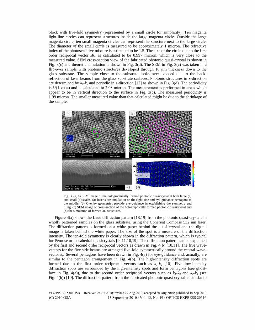
block with five-fold symmetry (represented by a small circle for simplicity). Ten magenta light-line circles can represent structures inside the large magenta circle. Outside the large magenta circle, ten small magenta circles can represent the structure next to the large circle. The diameter of the small circle is measured to be approximately 1 micron. The refractive index of the photosensitive mixture is estimated to be 1.5. The size of the circle due to the first order reciprocal vector Δkn is calculated to be 0.997 micron, which is very close to the measured value. SEM cross-section view of the fabricated photonic quasi-crystal is shown in Fig. 3(c) and theoretic simulation is shown in Fig. 3(d). The SEM in Fig. 3(c) was taken in a flip-over sample with photonic structures developed through 10 μm thickness down to the glass substrate. The sample close to the substrate looks over-exposed due to the back-reflection of laser beams from the glass substrate surfaces. Photonic structures in z-direction are determined by k0-kn and periodic in z-direction [12] as shown in Fig. 3(d). The periodicity is λ/(1-cosα) and is calculated to 2.08 micron. The measurement is performed in areas which appear to be in vertical direction to the surface in Fig. 3(c). The measured periodicity is 1.99 micron. The smaller measured value than that calculated might be due to the shrinkage of the sample.
Fig. 3. (a, b) SEM image of the holographically formed photonic quasicrystal at both large (a) and small (b) scales. (a) Inserts are simulation on the right side and eye-guidance pentagons in the middle. (b) Overlay geometries provide eye-guidance in establishing the symmetry and tiling. (c) SEM image of cross-section of the holographically formed photonic quasicrystal and (d) the simulation of formed 3D structures.
Figure 4(a) shows the Laue diffraction pattern [18,19] from the photonic quasi-crystals in wholly patterned samples on the glass substrate, using the Coherent Compass 532 nm laser. The diffraction pattern is formed on a white paper behind the quasi-crystal and the digital image is taken behind the white paper. The size of the spot is a measure of the diffraction intensity. The ten-fold symmetry is clearly shown in the diffraction pattern, which is typical for Penrose or icosahedral quasicrystals [9–11,18,19]. The diffraction pattern can be explained by the first and second order reciprocal vectors as drawn in Fig. 4(b) [10,11]. The five wave-vectors for the five side beams are arranged five-fold symmetrically around the central wave-vector k0. Several pentagons have been drawn in Fig. 4(a) for eye-guidance and, actually, are similar to the pentagon arrangement in Fig. 4(b). The high-intensity diffraction spots are formed due to the first order reciprocal vectors such as k1-k2 [10]. Five low-intensity diffraction spots are surrounded by the high-intensity spots and form pentagons (see ghost-face in Fig. 4(a)), due to the second order reciprocal vectors such as k1-k3 and k2-k4 (see Fig. 4(b)) [10]. The diffraction pattern from the fabricated photonic quasi-crystal is similar to
#132195 - $15.00 USD Received 26 Jul 2010; revised 29 Aug 2010; accepted 30 Aug 2010; published 10 Sep 2010(C) 2010 OSA 13 September 2010 / Vol. 18, No. 19 / OPTICS EXPRESS 20516
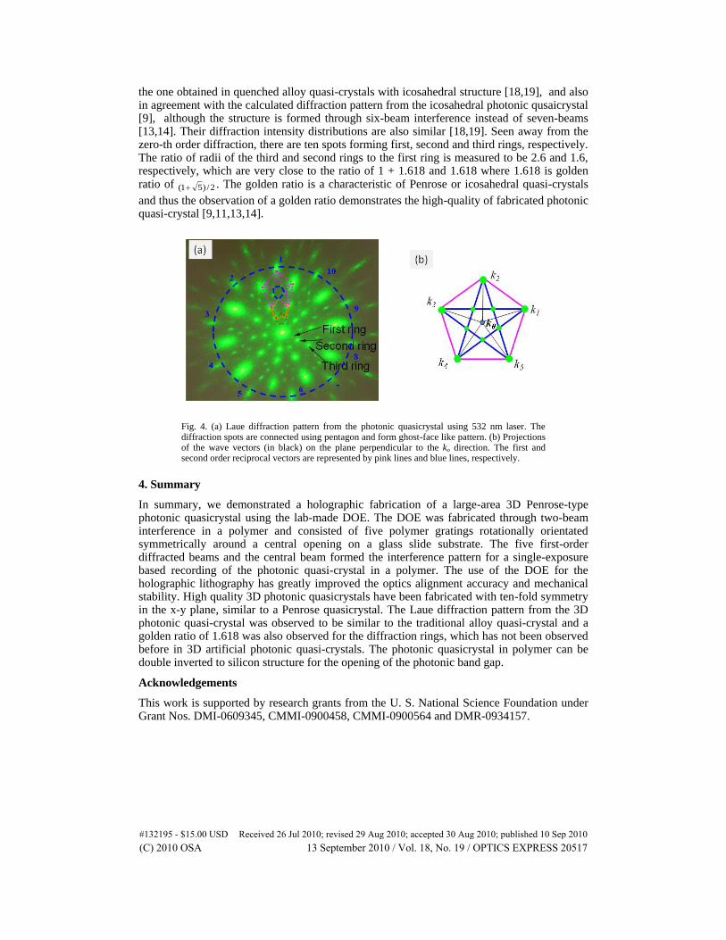
the one obtained in quenched alloy quasi-crystals with icosahedral structure [18,19], and also in agreement with the calculated diffraction pattern from the icosahedral photonic qusaicrystal [9], although the structure is formed through six-beam interference instead of seven-beams [13,14]. Their diffraction intensity distributions are also similar [18,19]. Seen away from the zero-th order diffraction, there are ten spots forming first, second and third rings, respectively. The ratio of radii of the third and second rings to the first ring is measured to be 2.6 and 1.6, respectively, which are very close to the ratio of 1 + 1.618 and 1.618 where 1.618 is golden ratio of 2/)51( . The golden ratio is a characteristic of Penrose or icosahedral quasi-crystals
and thus the observation of a golden ratio demonstrates the high-quality of fabricated photonic quasi-crystal [9,11,13,14].
Fig. 4. (a) Laue diffraction pattern from the photonic quasicrystal using 532 nm laser. The diffraction spots are connected using pentagon and form ghost-face like pattern. (b) Projections of the wave vectors (in black) on the plane perpendicular to the ko direction. The first and second order reciprocal vectors are represented by pink lines and blue lines, respectively.
4. Summary
In summary, we demonstrated a holographic fabrication of a large-area 3D Penrose-type photonic quasicrystal using the lab-made DOE. The DOE was fabricated through two-beam interference in a polymer and consisted of five polymer gratings rotationally orientated symmetrically around a central opening on a glass slide substrate. The five first-order diffracted beams and the central beam formed the interference pattern for a single-exposure based recording of the photonic quasi-crystal in a polymer. The use of the DOE for the holographic lithography has greatly improved the optics alignment accuracy and mechanical stability. High quality 3D photonic quasicrystals have been fabricated with ten-fold symmetry in the x-y plane, similar to a Penrose quasicrystal. The Laue diffraction pattern from the 3D photonic quasi-crystal was observed to be similar to the traditional alloy quasi-crystal and a golden ratio of 1.618 was also observed for the diffraction rings, which has not been observed before in 3D artificial photonic quasi-crystals. The photonic quasicrystal in polymer can be double inverted to silicon structure for the opening of the photonic band gap.
Acknowledgements
This work is supported by research grants from the U. S. National Science Foundation under Grant Nos. DMI-0609345, CMMI-0900458, CMMI-0900564 and DMR-0934157.
#132195 - $15.00 USD Received 26 Jul 2010; revised 29 Aug 2010; accepted 30 Aug 2010; published 10 Sep 2010(C) 2010 OSA 13 September 2010 / Vol. 18, No. 19 / OPTICS EXPRESS 20517