Embed Size (px)
Citation preview
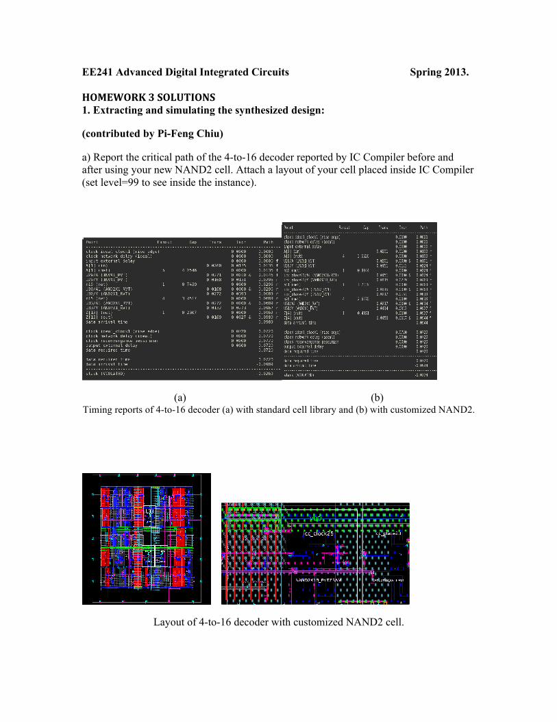
EE241 Advanced Digital Integrated Circuits Spring 2013. HOMEWORK 3 SOLUTIONS 1. Extracting and simulating the synthesized design:
(contributed by Pi-Feng Chiu)
a) Report the critical path of the 4-to-16 decoder reported by IC Compiler before and after using your new NAND2 cell. Attach a layout of your cell placed inside IC Compiler (set level=99 to see inside the instance).
(a) (b) Timing reports of 4-to-16 decoder (a) with standard cell library and (b) with customized NAND2.
Layout of 4-to-16 decoder with customized NAND2 cell.
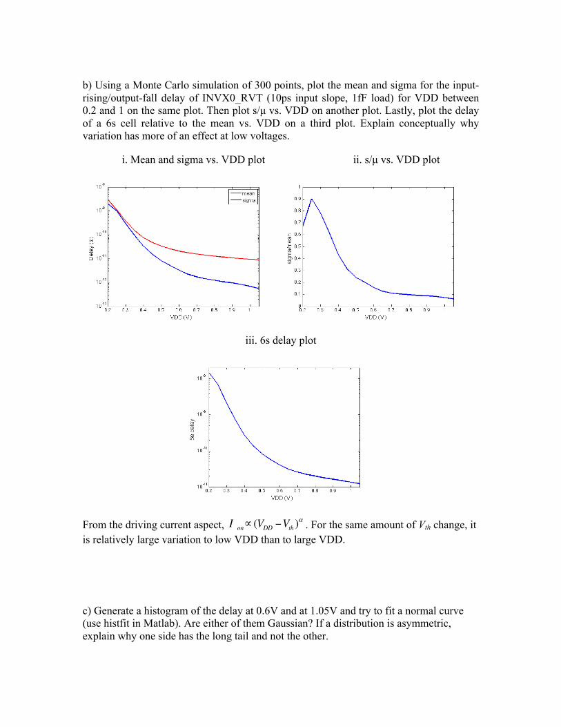
b) Using a Monte Carlo simulation of 300 points, plot the mean and sigma for the input- rising/output-fall delay of INVX0_RVT (10ps input slope, 1fF load) for VDD between 0.2 and 1 on the same plot. Then plot s/µ vs. VDD on another plot. Lastly, plot the delay of a 6s cell relative to the mean vs. VDD on a third plot. Explain conceptually why variation has more of an effect at low voltages.
i. Mean and sigma vs. VDD plot ii. s/µ vs. VDD plot
iii. 6s delay plot
From the driving current aspect, I on∝ (VDD −Vth )α . For the same amount of Vth change, it
is relatively large variation to low VDD than to large VDD.
c) Generate a histogram of the delay at 0.6V and at 1.05V and try to fit a normal curve (use histfit in Matlab). Are either of them Gaussian? If a distribution is asymmetric, explain why one side has the long tail and not the other.
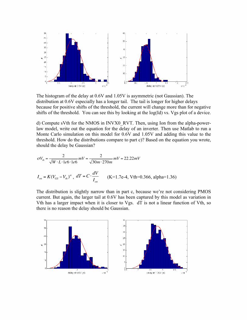
The histogram of the delay at 0.6V and 1.05V is asymmetric (not Gaussian). The distribution at 0.6V especially has a longer tail. The tail is longer for higher delays because for positive shifts of the threshold, the current will change more than for negative shifts of the threshold. You can see this by looking at the log(Id) vs. Vgs plot of a device.
d) Compute sVth for the NMOS in INVX0_RVT. Then, using Ion from the alpha-power-law model, write out the equation for the delay of an inverter. Then use Matlab to run a Monte Carlo simulation on this model for 0.6V and 1.05V and adding this value to the threshold. How do the distributions compare to part c)? Based on the equation you wrote, should the delay be Gaussian?
σVth =2
W ⋅L ⋅1e6 ⋅1e6mV =
230m ⋅270m
mV = 22.22mV
Ion = K(VGS −Vth )α , dT =C ⋅
dVIon
(K=1.7e-4, Vth=0.366, alpha=1.36)
The distribution is slightly narrow than in part c, because we’re not considering PMOS current. But again, the larger tail at 0.6V has been captured by this model as variation in Vth has a larger impact when it is closer to Vgs. dT is not a linear function of Vth, so there is no reason the delay should be Gaussian.
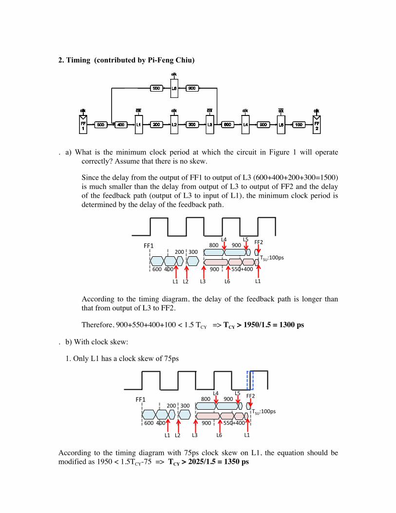
2. Timing (contributed by Pi-Feng Chiu)
. a) What is the minimum clock period at which the circuit in Figure 1 will operate correctly? Assume that there is no skew.
Since the delay from the output of FF1 to output of L3 (600+400+200+300=1500) is much smaller than the delay from output of L3 to output of FF2 and the delay of the feedback path (output of L3 to input of L1), the minimum clock period is determined by the delay of the feedback path.
600# 400#
200#FF1#
L1# L2#
300#
L3#
800# 900#
900#
L6# L1#
550+400#
L4# L5# FF2#
TSU:100ps#
According to the timing diagram, the delay of the feedback path is longer than that from output of L3 to FF2.
Therefore, 900+550+400+100 < 1.5 TCY => TCY > 1950/1.5 = 1300 ps
. b) With clock skew:
1. Only L1 has a clock skew of 75ps
600# 400#
200#FF1#
L1# L2#
300#
L3#
800# 900#
900#
L6# L1#
550+400#
L4# L5# FF2#
TSU:100ps#
According to the timing diagram with 75ps clock skew on L1, the equation should be modified as 1950 < 1.5TCY-75 => TCY > 2025/1.5 = 1350 ps
2. Only L2 has a clock skew of 75ps
600# 400#
200#FF1#
L1# L2#
300#
L3#
800# 900#
900#
L6# L1#
550+400#
L4# L5# FF2#
TSU:100ps#
According to the timing diagram, the delays before and after L2 are short compared to cycle time. Therefore, 75ps clock skew on L2 will not change the cycle time.
ð TCY > 1950/1.5 = 1300 ps
3. Flip-flops (contributed by Stevo Bailey)
Traditional FF:
l Clock to Q delay: 4tinv l Setup time: ttrans + tinv l Hold time: tinv l Switching energy: 4 diffusion pairs and 6 gate pairs (signal), 6 gate pairs (clock)
Because the flip-flop features two inverters to buffer the clock signal and generate an inverter clock signal, the timing of the FF suffers. To reach the output, the clock signal must first pass through both inverters, opening the second transmission gate. For simplicity, I assume that the data passes through this transmission gate at the same time as the clock passes through its second inverter. In this case, the transmission gate is only half on, but it should be enough time. Thus, the transmission gate delay is not included, and the data just has to pass through the next two inverters to reach the output.
To properly latch the data, the first latch (master) must grab the data completely. This means the correct input must pass through the first transmission gate and the next inverter to ensure no metastability ensues. Again assuming the data can pass through the input transmission gate while it is only half open, the setup time is one transmission gate plus two inverters minus the first clock inverter.
Pessimistically, a fast path preceding the FF may send incorrect data through the transmission gate even if it is half open. Thus, to ensure the proper data is latched, the clock must pass through both inverters before the data reaches the input transmission gate. The hold time is then two inverters minus the input inverter.
Switching energy is proportional to capacitance, so a rough estimate can easily be obtained by estimating the total capacitance. Clock nodes are separated from signal nodes because they always switch twice per cycle, while signal nodes may switch once per cycle or less. Transmission gates present diffusion capacitance, and inverters present gate capacitance.
Improved FF:
l Clock to Q delay: tpass + tinv + tfight l Setup time: 3tinv + tpass l Hold time: -tinv l Switching energy: 8 diffusion pairs and 9 gate pairs (signal), 2 gate pairs (clock)
To reach the output, data must pass through the NMOS pass gates, overcome the positive feedback of the two output cross-coupled inverters, and pass through the final output buffering inverter. I added a term, tfight, to represent the additional delay associated with switching nodes H and HN, overcoming the positive feedback. It should be relatively small.
Data must reach nodes G and GN to avoid metastability issues, so the setup time involves three inverters (input inverter, BN-to-B inverter, and the G and GN inverters) plus a PMOS pass gate. The two sets of parallel pass gates cross coupling the G and GN inverters are assumed to contribute negligible delay since they mostly remove the positive feedback during switching yet ensure F and FN remain well-defined.
Since this FF requires only one clock edge, data from a fast path can reach BN as the clock edge shuts off the PMOS pass gates. Thus the hold time is actually negative due to the input inverter.
Separating the clock and signal loads yields the above capacitance totals for the signal and clock paths. Comparison: The improved FF design has several benefits. First, it presents a smaller clock load, and we know the clock switches twice per cycle. Second, it has a reduced clock-to-Q delay. The differential nature of the FF allows it to reach the output quickly. Third, it has a negative hold time, although this may be a poor comparison as described later.
Pitfalls of the improved FF design include its higher setup time and higher signal switching energy. This design trades some setup time for clock-to-Q delay. It also has more complicated timing and sizing, since there exists cross-coupled inverter fights to overcome.
Finally, a note on the clock loading. Figure (a) presented a traditional FF with clock buffering inside the FF, while Figure (b) shows no clock buffering. To get a more accurate picture, clock loading and buffering should either be included in both designs or excluded in both designs. With excluding it, both designs would have the same hold time (-tinv), and the clock-to-Q delays would be comparable. Still, the improved design presents a smaller load to the clock network.