Embed Size (px)
Citation preview

© 2016 Freescale Semiconductor, Inc. All rights reserved.
How to Increase the Analog-to-Digital
Converter Accuracy in an Application
1. Overview
This document explains the analog-to-digital converter
(ADC) basics and the key parameters. The document
also lists the ADC errors sources and how to increase
ADC accuracy from system point of view.
This application note uses the ADC embedded in the
Kinetis microcontroller as an example. However the
same principles are applied to other ADCs too. The
accuracy of analog to digital conversion has an impact
on overall system quality and efficiency.
To be able to improve ADC accuracy, understand which
factors affect errors. The ADC itself, can’t fully ensure
the accuracy of results, it depends on the overall system
design.
For this reason, carefully prepare before starting your
development. Many factors including voltage reference,
PCB layout, I/O switching, and analog source
impedance and so on can affect the ADC accuracy
depending on the application.
2. ADC basics
2.1. Defining ADC
An analog-to-digital converter, or ADC, is a device or
peripheral that converts analog signals into digital
signals.
Freescale Semiconductor, Inc. Document Number: AN5250
Application Note Rev. 0 , 01/2016
Contents
1. Overview ............................................................................ 1 2. ADC basics ........................................................................ 1
2.1. Defining ADC ......................................................... 1 2.2. ADC block description ........................................... 2 2.3. ADC terminology ................................................... 4
3. ADC errors ......................................................................... 6 3.1. ADC errors related to itself ..................................... 6 3.2. ADC errors related to the whole system ................. 9
4. How to increase the ADC accuracy ................................. 12 4.1. Reduce the effects of the ADC-related errors ....... 12 4.2. Minimize the ADC errors related to the external
environment ........................................................................ 13 5. References ........................................................................ 19 6. Revision history ............................................................... 19

ADC basics
How to Increase the Analog-to-Digital Converter Accuracy in an Application, Application Note, Rev. 0, 01/2016
2 Freescale Semiconductor, Inc.
In the real world, signals mostly exist in analog form. You can use the ADC of the microcontroller to
sample such signals, so that the signals can be converted to the digital values. The application software
can then process the digital outputs and make decisions depending on the actual requirements.
The limitation imposed by the finite number of digital outputs decides how close the output is to the
analog input. In order to get closer between digital result and analog signal, the higher resolution of
ADC is needed.
2.2. ADC block description
There are several types of popular ADC blocks like SAR (successive approximation Register) ADC,
successive ADC, and SD (Sigma-Delta) ADC, and so on.
SAR ADC is used commonly in NXP Kinetis series products, and includes voltage reference,
conversion trigger control, SAR controller, calibration block, and conversion result processing. This
application note explains NXP SAR ADC.
The A/D conversion of SAR starts by forcing the MSB (Most Significant Bit) high. For example, in an
8-bit ADC it becomes 1000 0000, and the DAC converts it to VAREF/2. The analog comparator
compares the input voltage with VAREF/2. If the input voltage is greater than the voltage corresponding
to the MSB, the bit is left set, otherwise it is reset.
VAREF is the reference voltage used by ADC for conversions. After this comparison is done, the next
significant bit is set (=VAREF/4) and a comparison is done again with the input voltage. The procedure
is followed until all the bit positions are compared. The SAR ADC illustration is depicted as below
Figure 1.
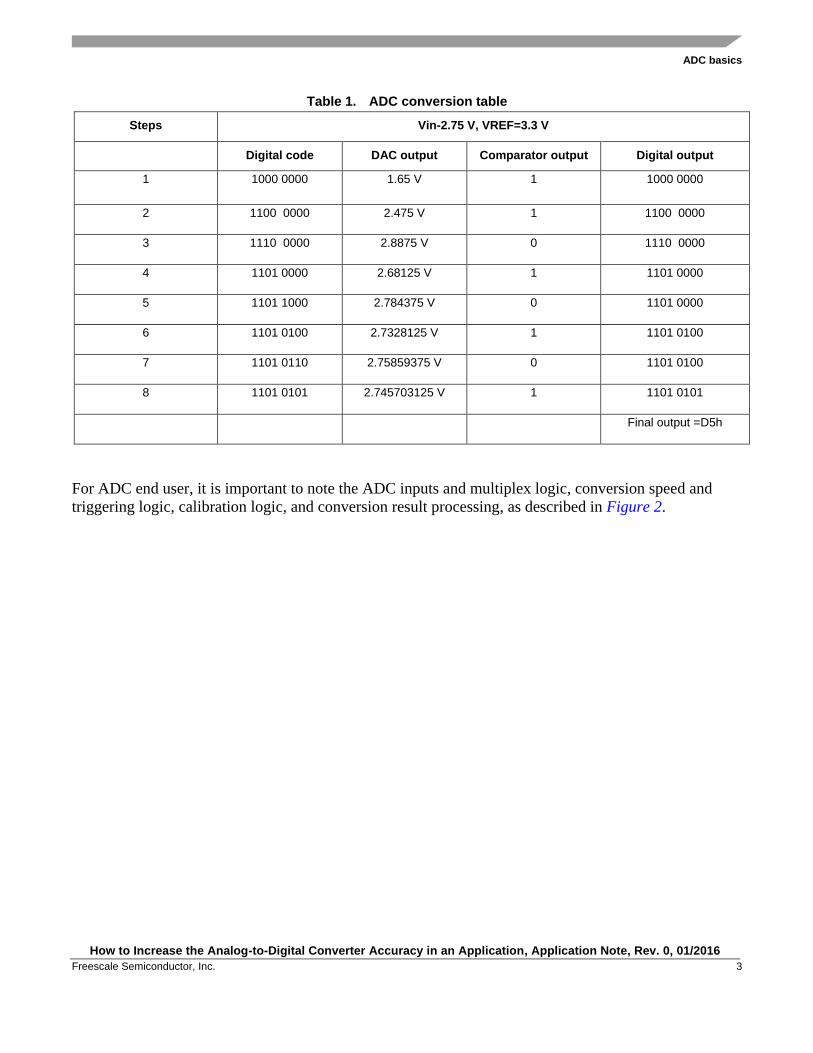
Figure 1. SAR ADC illustration
At the end of all the comparisons you get the corresponding digital output for the analog input. The
successive approximation steps are shown in Table 1. The digital output obtained from the ADC is D5h
when the analog input is 2.75 V.
ADC basics
How to Increase the Analog-to-Digital Converter Accuracy in an Application, Application Note, Rev. 0, 01/2016
Freescale Semiconductor, Inc. 3
Table 1. ADC conversion table
Steps Vin-2.75 V, VREF=3.3 V
Digital code DAC output Comparator output Digital output
1 1000 0000 1.65 V 1 1000 0000
2 1100 0000 2.475 V 1 1100 0000
3 1110 0000 2.8875 V 0 1110 0000
4 1101 0000 2.68125 V 1 1101 0000
5 1101 1000 2.784375 V 0 1101 0000
6 1101 0100 2.7328125 V 1 1101 0100
7 1101 0110 2.75859375 V 0 1101 0100
8 1101 0101 2.745703125 V 1 1101 0101
Final output =D5h
For ADC end user, it is important to note the ADC inputs and multiplex logic, conversion speed and
triggering logic, calibration logic, and conversion result processing, as described in Figure 2.

ADC basics
How to Increase the Analog-to-Digital Converter Accuracy in an Application, Application Note, Rev. 0, 01/2016
4 Freescale Semiconductor, Inc.
Figure 2. Kinetis SAR ADC block
2.3. ADC terminology
This section explains reference voltage, resolution, quantization, and sampling frequency.
2.3.1. Reference voltage
The ADC requires a reference voltage to which the analog input is compared to produce the digital
output. The digital output is the ratio of the analog input with respect to this reference voltage.

ADC basics
How to Increase the Analog-to-Digital Converter Accuracy in an Application, Application Note, Rev. 0, 01/2016
Freescale Semiconductor, Inc. 5
Digital value = (Analog input voltage)/ VAREF) * (2n-1)
Where n = number of bits of ADC digital output.
For example, for 12-bit ADC, VIN=1V, VAREF=3.3 V
Digital value = (1 V/3.3 V) *4095 = 1240d = 4D8h
2.3.2. Resolution
The ADC resolution is defined as the smallest incremental voltage that can be recognized and thus
causes a change in the digital output. It is expressed as the number of bits output by the ADC. Therefore,
an ADC which converts the analog signal to a 12-bit digital value has a resolution of 12 bits.
The smallest incremental voltage that can be recognized is expressed in terms of LSB.
1 LSB = (VAREF - VSS)/2n
Where LSB = Least-significant bit
n = Number of digital bits output by the ADC
VAREF = Reference voltage
VSS = Analog ground
An ADC which has ‘n’ bit digital output provides 2n digital values. It includes both 0 and 2
n-1.
With a 3.3 V reference voltage, the resolution is 3.3/212 = 3.3/4096 = 0.805 (mV).
2.3.3. Quantization
The quantization of an analog signal by the ADC can be processed only in the finite number of steps
which can be produced by the ADC.
The quantization error is the error introduced by the process of quantization. Ideally, any analog input
voltage can be maximum of 1/2 LSB away from its nearest digital code. Therefore, the quantization
error is 0.5 LSB for the ADC.
2.3.4. Sampling Frequency
The sampling frequency stand outs the speed to convert the analog signal to digital result. Therefore, the
ADC sampling frequency must be at least twice the analog signal frequency.
Sampling the signal at twice the analog signal frequency will not result in a loss of information.
If sampling frequency is less, then the information will be lost. This is a standard theorem that applies to
ADCs in general.
For example, an ADC with a conversion time of 10 μs can be used to sample an analog signal with a
time period of 20μs, i.e., 50 kHz.

ADC errors
How to Increase the Analog-to-Digital Converter Accuracy in an Application, Application Note, Rev. 0, 01/2016
6 Freescale Semiconductor, Inc.
3. ADC errors
This section lists the ADC errors related to itself and the whole system.
3.1. ADC errors related to itself
The ADC errors related to itself include: offset error, gain error, differential linearity error, integral
linearity error, and total unadjusted error.
3.1.1. Offset error
Offset error represented as EO is the difference between the actual and ideal first transition voltages as
described in Figure 3. This is the same definition as Zero-Scale Error.
Ideally, when the analog input is between 0.5 LSB and 1.5 LSB, the digital output should be ideally still
until the first transition occurs at 0.5 LSB. Offset error can easily be calibrated by the application
firmware.
Digital Output
VAIN
Ideal transfer curve
Actual transfer curve1
2
0.5LSB
Eo > 0
Figure 3. Offset error
3.1.2. Gain error
Gain error represented as EG is defined as the deviation between the last actual transition and the last
ideal transition described in Figure 4. The last actual transition is the transition from FFEh to FFFh.
Ideally, there should be a transition from FFEh to FFFh, when the analog input is equal to VAREF – 0.5
LSB. For VAREF = 3.3 V, the last ideal transition should be at 3.299597 V. If the ADC provides the
FFFh reading for VAIN < VAREF – 0.5LSB, then there is a negative gain error.
ADC errors
How to Increase the Analog-to-Digital Converter Accuracy in an Application, Application Note, Rev. 0, 01/2016
Freescale Semiconductor, Inc. 7
0.5LSB
EG > 0
Ideal transfer curve
Actual transfer curve
4094.5LSB
Digital Output
VAIN
4095
Figure 4. Gain error
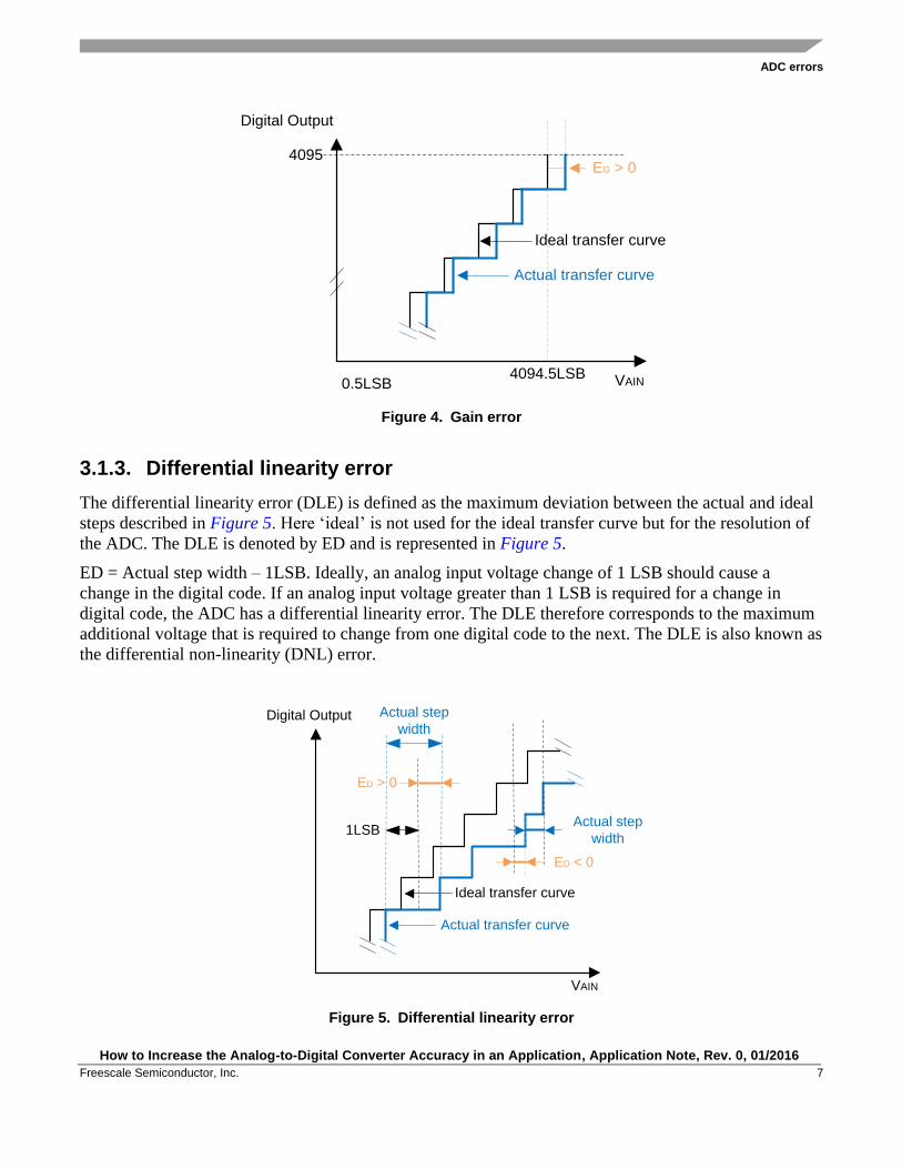
3.1.3. Differential linearity error
The differential linearity error (DLE) is defined as the maximum deviation between the actual and ideal
steps described in Figure 5. Here ‘ideal’ is not used for the ideal transfer curve but for the resolution of
the ADC. The DLE is denoted by ED and is represented in Figure 5.
ED = Actual step width – 1LSB. Ideally, an analog input voltage change of 1 LSB should cause a
change in the digital code. If an analog input voltage greater than 1 LSB is required for a change in
digital code, the ADC has a differential linearity error. The DLE therefore corresponds to the maximum
additional voltage that is required to change from one digital code to the next. The DLE is also known as
the differential non-linearity (DNL) error.
Ideal transfer curve
Actual transfer curve
Digital Output
VAIN
Actual step
width
ED < 0
Actual step
width
ED > 0
1LSB
Figure 5. Differential linearity error

ADC errors
How to Increase the Analog-to-Digital Converter Accuracy in an Application, Application Note, Rev. 0, 01/2016
8 Freescale Semiconductor, Inc.
3.1.4. Integral linearity error
The integral linearity error (ILE) is the maximum deviation between any actual transition and the
endpoint correlation line as described in Figure 6. The ILE is denoted by EL and is represented in
Figure 6. The endpoint correlation line can be defined as the line on the A/D transfer curve that connects
the first actual transition with the last actual transition. EL is the deviation from this line for each
transition. The endpoint correlation line thus corresponds to the actual transfer curve and has no relation
to the ideal transfer curve. The ILE is also known as the integral non linearity error (INL). The ILE is
the integral of the DLE over the whole range.
550 uV
EL
Actual transfer curve
3.298435V
Digital Output
VAIN
4095
1
2
Figure 6. Integral linearity error
3.1.5. Total unadjusted error
The total unadjusted error (TUE) is defined as the maximum deviation between the actual and the ideal
transfer curves described in Figure 7. It is a parameter that specifies the total errors that may occur,
causing maximum deviation between the ideal digital output and the actual digital output. It is the
maximum deviation recorded between the ideal expected value and the actual value obtained from the
ADC for any input voltage. The TUE is not the sum of EO, EG, EL, ED. The offset error affects the
digital result at lower voltages whereas the gain error affects the digital output for higher voltages.

ADC errors
How to Increase the Analog-to-Digital Converter Accuracy in an Application, Application Note, Rev. 0, 01/2016
Freescale Semiconductor, Inc. 9
Ideal transfer curve
Actual transfer curve
Digital Output
VAIN
ET
Figure 7. Total unadjusted error
3.2. ADC errors related to the whole system
The ADC errors related to the whole system includes: reference-voltage noise, analog-input signal noise,
ADC dynamic range, analog-signal source resistance, and temperature influence.
3.2.1. Reference-voltage noise
The ADC output is the ratio between the analog-signal voltage and the reference voltage. Any noise on
the analog reference causes a change in the converted digital value. For example, with an analog
reference of 3.3 V (VAREF = VDDA) and a 1 V signal input, the converted result is (1/3.3) × 4095 =
4D9h.
With a 40 mV peak-to-peak ripple in the analog reference, the converted value becomes (1/3.34) × 4095
= 4CAh (with VAREF at its peak).
Error = 4D9 – 4CA = 15 LSB. The SMPS (switch-mode power supply) normally has internal fast-
switching power transistors.
This introduces high-frequency noise in the output. The switching noise is in the range of 15 kHz to 1
MHz
3.2.2. Analog-input signal noise
Small but high-frequency signal variation can result in big conversion errors during sampling time. This
noise is generated by electrical devices. For example, power lines and the transformers affect the source
signal (for example a sensor) by adding an unwanted signal. As a consequence, the conversion results of
the ADC are not accurate.
From below Figure 8, you can see the actual analog input signal have some inducted 5mV Vpp noise,
which loses 2 LSB for 10-bit resolution ADC.

ADC errors
How to Increase the Analog-to-Digital Converter Accuracy in an Application, Application Note, Rev. 0, 01/2016
10 Freescale Semiconductor, Inc.
Figure 8. Analog input signal
3.2.3. ADC dynamic range
To have the maximum ADC conversion precision, it is preferable that the ADC dynamic range matches
the maximum amplitude of the signal. Assume that the signal to be converted varies between 0 V to 2.5
V and that VAREF is equal to 3.3 V. The maximum signal value converted by the ADC is 3102 (2.5 V)
as shown in Figure 9. In this case, there are 993 unused transitions (4095 – 3102 = 993). This implies a
loss in the converted signal accuracy especially if the ADC lineaty performance is not ideal.
V
t
Unused ADC translation range
2.5V
(3102h)
Vref = 3.3V
(4095h)
Figure 9. ADC dynamic range
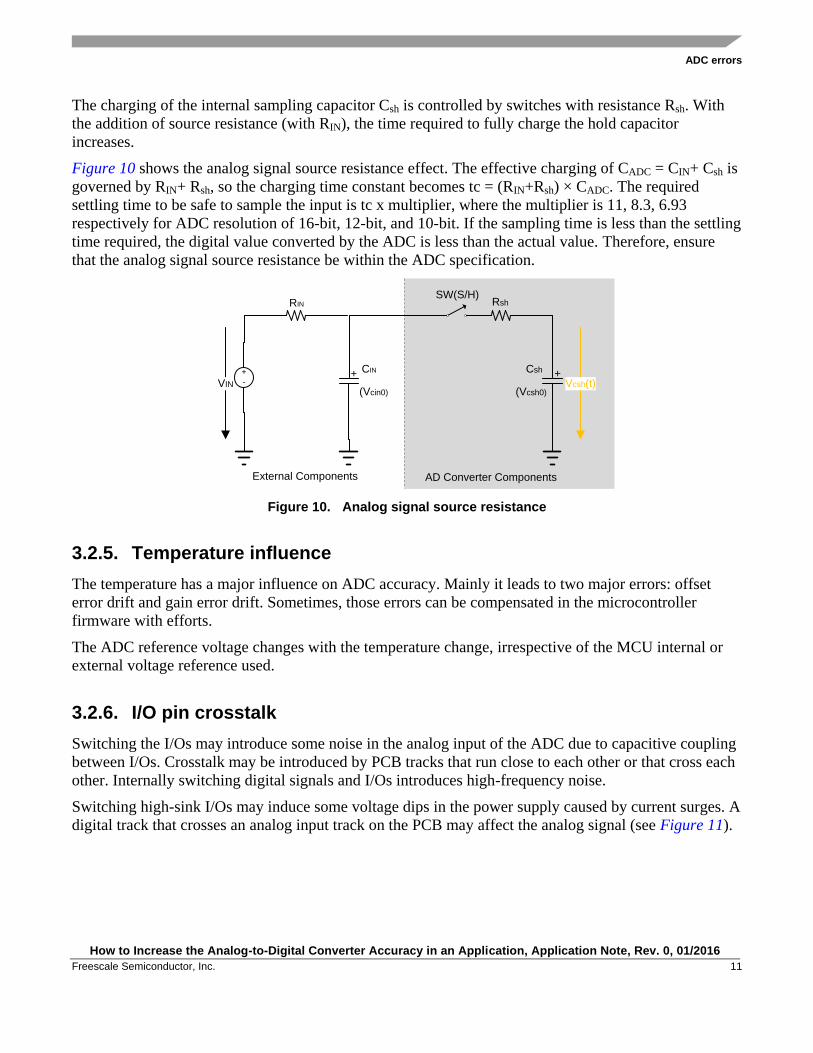
3.2.4. Analog-signal source resistance
The impedance of the analog-signal source or series resistance (RIN) between the source and the pin
causes a voltage drop across it because of the current flowing into the pin.
ADC errors
How to Increase the Analog-to-Digital Converter Accuracy in an Application, Application Note, Rev. 0, 01/2016
Freescale Semiconductor, Inc. 11
The charging of the internal sampling capacitor Csh is controlled by switches with resistance Rsh. With
the addition of source resistance (with RIN), the time required to fully charge the hold capacitor
increases.
Figure 10 shows the analog signal source resistance effect. The effective charging of CADC = CIN+ Csh is
governed by RIN+ Rsh, so the charging time constant becomes tc = (RIN+Rsh) × CADC. The required
settling time to be safe to sample the input is tc x multiplier, where the multiplier is 11, 8.3, 6.93
respectively for ADC resolution of 16-bit, 12-bit, and 10-bit. If the sampling time is less than the settling
time required, the digital value converted by the ADC is less than the actual value. Therefore, ensure
that the analog signal source resistance be within the ADC specification.
+
-+ +
RIN RshSW(S/H)
CIN Csh
(Vcin0) (Vcsh0)VIN Vcsh(t)
External Components AD Converter Components
Figure 10. Analog signal source resistance
3.2.5. Temperature influence
The temperature has a major influence on ADC accuracy. Mainly it leads to two major errors: offset
error drift and gain error drift. Sometimes, those errors can be compensated in the microcontroller
firmware with efforts.
The ADC reference voltage changes with the temperature change, irrespective of the MCU internal or
external voltage reference used.
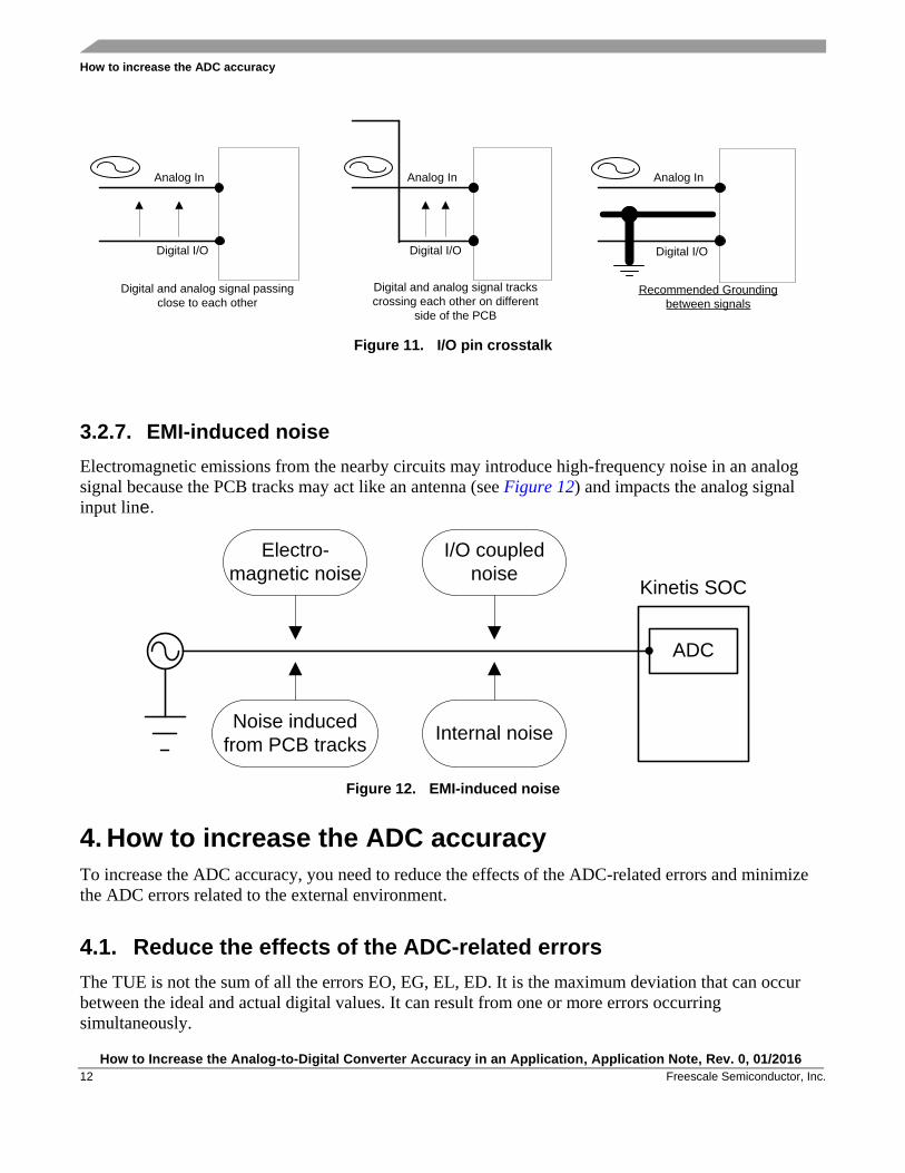
3.2.6. I/O pin crosstalk
Switching the I/Os may introduce some noise in the analog input of the ADC due to capacitive coupling
between I/Os. Crosstalk may be introduced by PCB tracks that run close to each other or that cross each
other. Internally switching digital signals and I/Os introduces high-frequency noise.
Switching high-sink I/Os may induce some voltage dips in the power supply caused by current surges. A
digital track that crosses an analog input track on the PCB may affect the analog signal (see Figure 11).
How to increase the ADC accuracy
How to Increase the Analog-to-Digital Converter Accuracy in an Application, Application Note, Rev. 0, 01/2016
12 Freescale Semiconductor, Inc.
Digital and analog signal passing
close to each other
Digital I/O
Analog In
Recommended Grounding
between signals
Analog In
Digital I/O
Digital and analog signal tracks
crossing each other on different
side of the PCB
Analog In
Digital I/O
Figure 11. I/O pin crosstalk
3.2.7. EMI-induced noise
Electromagnetic emissions from the nearby circuits may introduce high-frequency noise in an analog
signal because the PCB tracks may act like an antenna (see Figure 12) and impacts the analog signal
input line.
Electro-
magnetic noise
I/O coupled
noise
Internal noiseNoise induced
from PCB tracks
Kinetis SOC
ADC
Figure 12. EMI-induced noise
4. How to increase the ADC accuracy
To increase the ADC accuracy, you need to reduce the effects of the ADC-related errors and minimize
the ADC errors related to the external environment.
4.1. Reduce the effects of the ADC-related errors
The TUE is not the sum of all the errors EO, EG, EL, ED. It is the maximum deviation that can occur
between the ideal and actual digital values. It can result from one or more errors occurring
simultaneously.

How to increase the ADC accuracy
How to Increase the Analog-to-Digital Converter Accuracy in an Application, Application Note, Rev. 0, 01/2016
Freescale Semiconductor, Inc. 13
As the ILE is the integral of the DLE, it can be considered as the indicator of the maximum error. Do not
add the DLE and ILE together to calculate the maximum error that may occur at any digital step.
The maximum error values specified in the datasheet are the worst error values measured in laboratory
test environment over the given voltage and temperature range.
The ILE and DLE are dependent on the ADC design. It is difficult to calibrate them. They can be
calibrated by the measured ADC curve stored in the microcontroller memory but this needs calibration
of each individual device in final application.
Offset and gain errors can be compensated using the Kinetis ADC self-calibration feature or by
microcontroller firmware.
4.2. Minimize the ADC errors related to the external environment
To minimize the ADC errors related to the external environment, take care of the reference voltage and
power supply, eliminate the analog-input signal noise, match the ADC dynamic range to the maximum
signal amplitude, and match analog-source resistance. Additionally, minimize the I/O pin crosstalk,
check temperature effect compensation, reduce EMI-induced noise, make recommended PCB layout
changes, and use software methods to improve precision.
4.2.1. Reference voltage and Power supply
The power supply should have a good line, load regulation, and temperature drift since the ADC uses
VAREF or VDDA as the analog reference. Also, the digital value is the ratio of the analog input signal
to this voltage reference.
Thus, it is essential for VAREF to remain stable at different loads. Whenever, the load is increased by
switching on a part of the circuit, the increase in current should not cause the voltage to decrease.
If the voltage remains stable over a wide current range, the power supply has good load regulation. For
example, for the SPX3819 voltage regulator, the line regulation is 0.04 % typical when VIN varies from
VOUT + 1 V to 16 V , and the load regulation is 0.05 % when the load varies from 0.1 mA to 500 mA.
The lower the line regulation value, the better the regulation.
Similarly, the lower the load regulation value, the better the regulation and the stability of the voltage
output. It is also possible to use a reference voltage for VAREF , for instance the AD780, which is a
high precision voltage reference of 2.5 V.
Temperature drift is another important factor to consider voltage reference, especially in some
application, the ADC accuracy is specified within full temp range.
4.2.2. Analog-input signal noise elimination
Eliminate the analog-input signal noise by using the averaging method or by adding an external filter.

How to increase the ADC accuracy
How to Increase the Analog-to-Digital Converter Accuracy in an Application, Application Note, Rev. 0, 01/2016
14 Freescale Semiconductor, Inc.
4.2.2.1. Averaging method
Averaging is a simple technique where you sample an analog input several times and take the average of
the results by software. This technique is helpful to eliminate the effect of noise on the analog input in
case of an analog voltage that does not change frequently.
The average is made on several readings that correspond to the same analog-input voltage. Ensure that
the analog input remains at the same voltage during the time period until the conversions are done.
Otherwise, you add up digital values corresponding to different analog inputs and can introduce errors.
4.2.2.2. Adding an external filter
Adding an external RC filter eliminates the high frequency noise. An expensive filter is not needed to
deal with a signal that has frequency components above the frequency range of interest. In this case, a
relatively low cost low pass filter with a cutoff frequency fC just above the frequency range of interest
will be sufficient to limit the noise. A sampling rate consistent with the highest frequency of interest will
suffice, typically 2 to 5 times fC.
4.2.3. Matching the ADC dynamic range to the maximum signal amplitude
This method improves accuracy by a proper selection of the reference voltage or by using a preamplifier
stage to obtain the maximum possible resolution using the full ADC output range.
The reference voltage is selected in the expected range of the signal to be measured. If the measured
signal has an offset, then the reference voltage should also have a similar offset. If the measured signal
has defined maximum amplitude, then the reference voltage should also have a similar maximum value.
By matching this reference voltage to the measurement signal range, we obtain the maximum possible
resolution using the full ADC output range.
In Kinetis device, the ADC reference voltage is connected to the external VREFH and VREFL pins that
should be tied to ground. This makes it possible to match the reference voltage and the measured signal
range. For example, if the measured signal varies between 0 V and 2.5 V, it is recommended to choose
VREFH = 2.5 V, possibly using a reference voltage like AD780.
4.2.4. Analog source resistance match
The impedance of the analog signal source or series resistance (RAIN), between the source and pin
causes a voltage drop across it because of the current flowing into the pin. The charging of the internal
sampling capacitor CADC is controlled by switches with resistance RADC. With the addition of source
resistance (with RADC), the time required to fully charge the hold capacitor increases.
Figure 13 shows the analog signal source resistance effect. The effective charging of CADC is governed
by RADC + RAIN, so the charging time constant becomes tc = (RADC+RAIN) × CADC. The required settling
time to be safe to sample the input is tc x multiplier, where the multiplier is 11, 8.3, 6.93 respectively for
the ADC resolution of 16-bit, 12-bit, and 10-bit. If the sampling time is less than the settling time
required, the digital value converted by the ADC is less than the actual value. The software configures

How to increase the ADC accuracy
How to Increase the Analog-to-Digital Converter Accuracy in an Application, Application Note, Rev. 0, 01/2016
Freescale Semiconductor, Inc. 15
the sampling time to be longer than the settle time. For more information on settling time, see the
AN4373. Always ensure that the analog signal source resistance be within the ADC specification.
Kinetis MCU
12-bit ADC
+
RADC
+- VSSA
RAIN
AINx+
-
VAIN
Vc
ttc
VAIN
Figure 13. Analog source resistance match
4.2.5. Minimizing I/O pin crosstalk
The noise produced by crosstalk can be reduced by shielding the analog signal by placing ground tracks
across it. Figure 14 shows the recommended grounding between signals.
Digital and analog signal passing
close to each other
Digital I/O
Analog In
Recommended Grounding
between signals
Analog In
Digital I/O
Digital and analog signal tracks
crossing each other on different
side of the PCB
Analog In
Digital I/O
Figure 14. I/O pin crosstalk

How to increase the ADC accuracy
How to Increase the Analog-to-Digital Converter Accuracy in an Application, Application Note, Rev. 0, 01/2016
16 Freescale Semiconductor, Inc.
4.2.6. Temperature effect compensation
One method is to fully characterize the offset, gain drift, and provide a lookup table in memory to
correct the measurements according to temperature change. This calibration involves additional cost and
takes time.
So in some cases such as metering, it is very important to provide low temperature drift voltage
reference, if temperature drift coefficient is too high, to full temp error will be higher accordingly.
4.2.7. EMI-induced noise reduction
Reduce EMI-noise by using proper shielding and layout techniques. The possible sources of emission
must be physically separated from the receptors. They can be separated electrically by proper grounding
and shielding.
Shielding technique placing ground tracks alongside sensitive analog signals provides shielding on the
PCB. The other side of the two-layer PCB should also have a ground plane. This prevents interference
and I/O crosstalk affecting the signal. See Figure 15. Signals coming from distant locations (like sensors,
etc.) should be connected to the PCB using shielded cable.
The shield should not be used to carry the ground reference from the sensor or analog source to the
microcontroller. A separate wire should be used as ground and the shield should be grounded at only one
place near the receiver such as the analog ground of the microcontroller.
Grounding the shield at both ends (source and receiver) might lead to the creation of ground loops, with
the result of current flowing through the shield. In this case, the shield acts like an antenna and the
purpose of the shielding is lost.
The shielding concept also applies to grounding the chassis of the application if it is metallic. And it also
helps remove EMI and EMC interference. In this case the mains earth ground is used to shield the
chassis. Similarly DC ground can be used for shielding in case of the earth ground not being available.
ADC ADC
Sensor Sensor
Shield cableNot recommended Recommended
Ground Loop
Do not ground the shield at both ends Ground the shield at the receiver end only
Figure 15. EMI-induced noise

How to increase the ADC accuracy
How to Increase the Analog-to-Digital Converter Accuracy in an Application, Application Note, Rev. 0, 01/2016
Freescale Semiconductor, Inc. 17
4.2.8. PCB layout recommendations
The PCB layout recommendations include separating the analog and digital layouts, separating the
power supplies for the analog and digital circuits, and component placement and routing.
4.2.8.1. Separating the analog and digital layouts
It is recommended to separate the analog and digital circuitry on the PCB (see Figure 16). This also
avoids tracks crossing each other. The tracks carrying digital signals may introduce high-frequency
noise in analog signals because of coupling.
The digital signals produce high-frequency noise because of fast switching. Coupling of a capacitive
nature is formed due to the metal connections (tracks) separated by the dielectric provided by the PCB
base (glass, ceramic or plastic).
It is recommended to use different planes for analog and digital grounds. If there is a lot of analog
circuitry then an analog ground plane is recommended. The analog ground must be placed below the
analog circuitry.
BA
CD
A1 B1
C1D1
Digital
Ground
Analog
Ground
Analog circuitry
(Affected by noise)
Digital circuitry
(Noise and noise
generating)
Power supply
Micro
controller
Figure 16. Separate layout
4.2.8.2. Separating the power supplies for the analog and digital circuits
It is desirable to have separate analog and digital power supplies in cases where there is a lot of analog
and digital circuits external to the microcontroller (see Figure 17).
If you use a switching-type power supply for the digital circuitry, you should use a separate linear
supply for the analog circuit. Also, if you expect a lot of noise on the DC power supply due to I/O
switching etc., it is preferable to use a separate supply for the analog circuit.
Also it is recommended to use star typology to supply power for analog and digital circuits to avoid
interference between each other.
How to increase the ADC accuracy
How to Increase the Analog-to-Digital Converter Accuracy in an Application, Application Note, Rev. 0, 01/2016
18 Freescale Semiconductor, Inc.
Figure 17. Separate power supply
4.2.8.3. Component placement and routing
Place the components and route the signal traces on the PCB so as to shield analog inputs. Components
like resistors and capacitors must be connected with very short leads. You can use surface-mounted
device (SMD) resistors and capacitors. You can place SMD capacitors close to the microcontroller for
decoupling purposes.
Use wide tracks for power; otherwise the series resistance of the tracks would cause a voltage drop.
Indeed, narrow power tracks have a non-negligible finite resistance, so that high load currents through
them would cause a voltage drop across them.
Quartz crystals must be surrounded by ground/guard ring. The other side of the two-layer PCB below
the crystal should preferably be covered by the ground plane or even cut off. Most crystals have a
metallic body that should be grounded. You should also place the crystal close to the microcontroller.
4.2.9. Software methods to improve precision
The precision of sampling depends on both software and hardware modules. It is not possible to get an
ideal precision with only one of them.
4.2.9.1. Averaging samples
This averaging decreases speed but can give improved accuracy.
SAR-ADC provides register settings to do hardware averaging.
The hardware averaging and software averaging are similar. Hardware averaging is faster, but it does
not provide more precision than software averaging.
Digital filtering (50/60 Hz suppression from DC value) – set proper sampling frequency (the trigger
from timer is useful in this case) – perform software post-processing on sampled data (for example,
comb filter - for 50 Hz noise and its harmonics suppression).

Revision history
How to Increase the Analog-to-Digital Converter Accuracy in an Application, Application Note, Rev. 0, 01/2016
Freescale Semiconductor, Inc. 19
4.2.9.2. Increase over-sampling-rate
Increase OSR (over-sampling-rate) can improve the precision.
The OSR can be adjusted in register settings.
4.2.9.3. Fast Fourier Transform (FFT) for AC measurements
This is to show harmonic parts in measured signal, which become slower, due to the use of more
computation power.
4.2.9.4. Calibration of ADC
The offset, the gain, and the bit weight calibration decreases the internal ADC errors. However, the
internal ADC structure must be known.
4.2.9.5. Minimizing internal noise generated by CPU
Design firmware to use minimum disturbance from microcontroller during ADC conversion - digital
silence. Use of ADC internal asynchronous clock as ADC clock will greatly reduce the digital noise
coupled to the ADC. If possible, let ADC convert samples in low power mode.
5. References
Following references are available on www.nxp.com:
1. MPC57xx SAR ADC Implementation and Use (Document: AN4881)
2. Filter-Based Algorithm for Metering Applications (Document: AN4265)
3. FFT-Based Algorithm for Metering Applications (Document: AN4255)
4. Using the FFT on the Sigma-Delta ADCs (Document: AN4847)
5. Cookbook for SAR ADC Measurements (Document: AN4373)
6. Revision history
Table 2 is the revision history table.
Table 2. Revision history
Revision number Date Substantive changes
0 01/2016 Initial release

Document Number: AN5250 Rev. 0
01/2016
How to Reach Us:
Home Page:
freescale.com
Web Support:
freescale.com/support
Information in this document is provided solely to enable system and software implementers to
use Freescale products. There are no express or implied copyright licenses granted hereunder to
design or fabricate any integrated circuits based on the information in this document.
Freescale reserves the right to make changes without further notice to any products herein.
Freescale makes no warranty, representation, or guarantee regarding the suitability of its
products for any particular purpose, nor does Freescale assume any liability arising out of the
application or use of any product or circuit, and specifically disclaims any and all liability,
including without limitation consequential or incidental damages. “Typical” parameters that may
be provided in Freescale data sheets and/or specifications can and do vary in different
applications, and actual performance may vary over time. All operating parameters, including
“typicals,” must be validated for each customer application by customer's technical experts.
Freescale does not convey any license under its patent rights nor the rights of others. Freescale
sells products pursuant to standard terms and conditions of sale, which can be found at the
following address: freescale.com/SalesTermsandConditions.
Freescale, the Freescale logo, and Kinetis are trademarks of Freescale Semiconductor, Inc., Reg.
U.S. Pat. & Tm. Off. All other product or service names are the property of their respective
owners. ARM, the ARM Powered logo, and Cortex are registered trademarks of ARM Limited
(or its subsidiaries) in the EU and/or elsewhere. All rights reserved.
© 2016 Freescale Semiconductor, Inc.
.