Embed Size (px)
Citation preview

Application ReportSLVA278–September 2007
How to use TI’s Set of Power RulersJuergen Schneider ......................................................................................... High Performance Analog
ABSTRACTWhile many experienced designers know all there is to know about power design, agrowing number of designers are confronted daily with unfamiliar power topics that areeither completely new to them, or last encountered years before.
The Power Rulers and this application note provide important rules of thumb and manyapproximated values. While they are sufficient for a first estimate, the use of moreaccurate numbers and equations should be considered when exact results arerequired.
This document describes how to use the four Power Rulers, and gives additionalbackground information for the topics covered on the rulers.
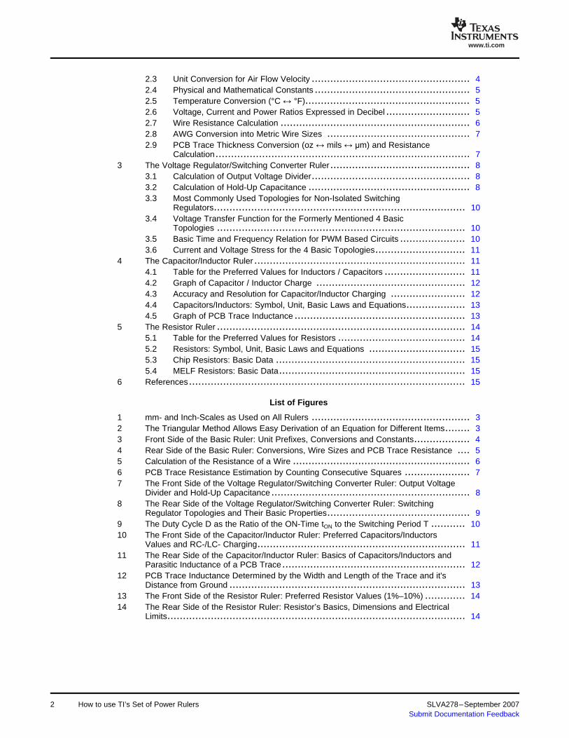
Contents1 General Information ................................................................................ 2
1.1 Separation of Dedicated Rulers ......................................................... 31.2 Scales ....................................................................................... 31.3 Triangle Method to Derive Formula Variations ........................................ 3
2 The Basic Ruler..................................................................................... 42.1 SI Prefixes .................................................................................. 42.2 Unit Conversions: Length, Volume, Speed, Power, Energy, Weight, Area ........ 4
SLVA278–September 2007 How to use TI’s Set of Power Rulers 1Submit Documentation Feedback
www.ti.com
2.3 Unit Conversion for Air Flow Velocity ................................................... 42.4 Physical and Mathematical Constants .................................................. 52.5 Temperature Conversion (°C ↔ °F)..................................................... 52.6 Voltage, Current and Power Ratios Expressed in Decibel ........................... 52.7 Wire Resistance Calculation ............................................................. 62.8 AWG Conversion into Metric Wire Sizes .............................................. 72.9 PCB Trace Thickness Conversion (oz ↔ mils ↔ μm) and Resistance
Calculation.................................................................................. 73 The Voltage Regulator/Switching Converter Ruler............................................. 8
3.1 Calculation of Output Voltage Divider................................................... 83.2 Calculation of Hold-Up Capacitance .................................................... 83.3 Most Commonly Used Topologies for Non-Isolated Switching
Regulators................................................................................. 103.4 Voltage Transfer Function for the Formerly Mentioned 4 Basic
Topologies ................................................................................ 103.5 Basic Time and Frequency Relation for PWM Based Circuits ..................... 103.6 Current and Voltage Stress for the 4 Basic Topologies............................. 11
4 The Capacitor/Inductor Ruler .................................................................... 114.1 Table for the Preferred Values for Inductors / Capacitors .......................... 114.2 Graph of Capacitor / Inductor Charge ................................................ 124.3 Accuracy and Resolution for Capacitor/Inductor Charging ........................ 124.4 Capacitors/Inductors: Symbol, Unit, Basic Laws and Equations................... 134.5 Graph of PCB Trace Inductance ....................................................... 13
5 The Resistor Ruler ................................................................................ 145.1 Table for the Preferred Values for Resistors ......................................... 145.2 Resistors: Symbol, Unit, Basic Laws and Equations ............................... 155.3 Chip Resistors: Basic Data ............................................................. 155.4 MELF Resistors: Basic Data............................................................ 15
6 References......................................................................................... 15
List of Figures
1 mm- and Inch-Scales as Used on All Rulers ................................................... 32 The Triangular Method Allows Easy Derivation of an Equation for Different Items........ 33 Front Side of the Basic Ruler: Unit Prefixes, Conversions and Constants.................. 44 Rear Side of the Basic Ruler: Conversions, Wire Sizes and PCB Trace Resistance .... 55 Calculation of the Resistance of a Wire ......................................................... 66 PCB Trace Resistance Estimation by Counting Consecutive Squares ..................... 77 The Front Side of the Voltage Regulator/Switching Converter Ruler: Output Voltage
Divider and Hold-Up Capacitance ................................................................ 88 The Rear Side of the Voltage Regulator/Switching Converter Ruler: Switching
Regulator Topologies and Their Basic Properties.............................................. 99 The Duty Cycle D as the Ratio of the ON-Time tON to the Switching Period T ........... 1010 The Front Side of the Capacitor/Inductor Ruler: Preferred Capacitors/Inductors
Values and RC-/LC- Charging................................................................... 1111 The Rear Side of the Capacitor/Inductor Ruler: Basics of Capacitors/Inductors and
Parasitic Inductance of a PCB Trace........................................................... 1212 PCB Trace Inductance Determined by the Width and Length of the Trace and it's
Distance from Ground ............................................................................ 1313 The Front Side of the Resistor Ruler: Preferred Resistor Values (1%–10%) ............. 1414 The Rear Side of the Resistor Ruler: Resistor’s Basics, Dimensions and Electrical
Limits................................................................................................ 14
2 How to use TI’s Set of Power Rulers SLVA278–September 2007Submit Documentation Feedback
www.ti.com
1 General Information
1.1 Separation of Dedicated Rulers
1.2 Scales
1.3 Triangle Method to Derive Formula Variations
General Information
The 4 rulers are supplied on a plastic ring that may be opened to separate them from each other.
Each ruler has a 15-cm metric scale and a 6-inch scale to allow easy measurement of length in the Metricas well as in the Imperial, or English system.
Figure 1. mm- and Inch-Scales as Used on All Rulers
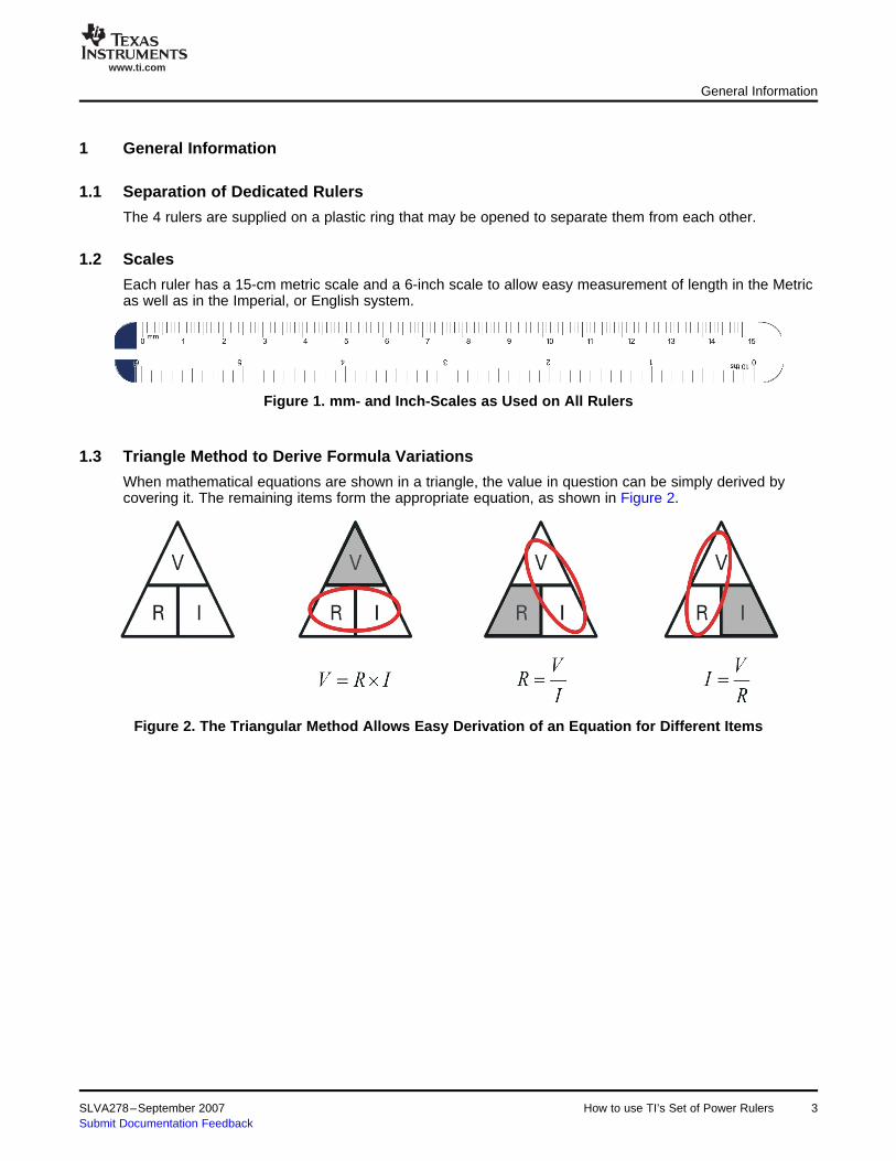
When mathematical equations are shown in a triangle, the value in question can be simply derived bycovering it. The remaining items form the appropriate equation, as shown in Figure 2.
Figure 2. The Triangular Method Allows Easy Derivation of an Equation for Different Items
SLVA278–September 2007 How to use TI’s Set of Power Rulers 3Submit Documentation Feedback

www.ti.com
2 The Basic Ruler
2.1 SI Prefixes
2.2 Unit Conversions: Length, Volume, Speed, Power, Energy, Weight, Area
2.3 Unit Conversion for Air Flow Velocity
The Basic Ruler
Figure 3. Front Side of the Basic Ruler: Unit Prefixes, Conversions and Constants
This table lists all the SI prefixes from femto to tera.
Conversions are given in this section for length, volume, speed, power, energy, weight/mass and area. Inaddition to these conversions, the following conversions are also useful:
• Length:– 1 foot (ft, ‘) = 1/3 yd = 12 in = 0.3048 m– 1 micron (μm, μ) = 1 micrometer (μm, μ)
Sometimes the symbol "um" is used instead of "μm".• Area:
– 1 square foot (sq ft, ft2) = 144 in2 = 929.03 cm2
Air-flow velocity units are often encountered when dealing with SOA (safe operating area) graphs forDC/DC converters. LFM stands for Linear Feet per Minute.
How to use TI’s Set of Power Rulers4 SLVA278–September 2007Submit Documentation Feedback

www.ti.com
2.4 Physical and Mathematical Constants
2.5 Temperature Conversion (°C ↔ °F)
( )32T9
5T FC -= °°
(1)
2.6 Voltage, Current and Power Ratios Expressed in Decibel
XdB 20 log10 XX0
(2)
XdB 10 log10 XX0
(3)
The Basic Ruler
• Permittivity and permeability of free space• Pi and Euler’s number
Figure 4. Rear Side of the Basic Ruler: Conversions, Wire Sizes and PCB Trace Resistance
This diagram relates the 0° and the 100° points for each scale to each other as well as some exemplaryvalues. To convert other values, Equation 1 (also printed above the temperature diagram on the ruler) canbe used. The term 5/9 in this equation comes from the fact that the freezing and the boiling points of waterare 100° apart on Celsius scale, and 180° apart on the Fahrenheit scale.
Ratios such as amplifier gain or filter attenuation are often expressed in decibels (dB). The table on theruler lists example values calculated using these equations:
for voltage and current ratios, and
for power ratios.
SLVA278–September 2007 How to use TI’s Set of Power Rulers 5Submit Documentation Feedback
www.ti.com
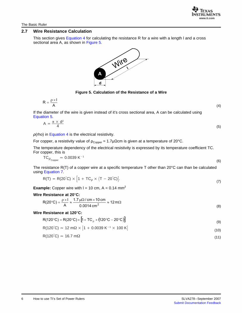
2.7 Wire Resistance Calculation
Wire
l
A
d
A
lR
´r=
(4)
A d2
4 (5)
TCCopper 0.0039 K1
(6)
R(T) R(20°C) 1 TC T 20°C).(7)
W»´Wm
»´r
=° m12cm0014.0
cm10cm/7.1
A
l)C20(R
2 (8)
( )[ ]C20C120TC1)C20(R)C120(R °-°´+´°=° r (9)
R(120°C) 12 m 1 0.0039 K1 100 K(10)
R(120°C) 16.7 m (11)
The Basic Ruler
This section gives Equation 4 for calculating the resistance R for a wire with a length l and a crosssectional area A, as shown in Figure 5.
Figure 5. Calculation of the Resistance of a Wire
If the diameter of the wire is given instead of it’s cross sectional area, A can be calculated usingEquation 5.
ρ(rho) in Equation 4 is the electrical resistivity.
For copper, a resistivity value of ρCopper ≈ 1.7μΩcm is given at a temperature of 20°C.
The temperature dependency of the electrical resistivity is expressed by its temperature coefficient TC.For copper, this is
The resistance R(T) of a copper wire at a specific temperature T other than 20°C can than be calculatedusing Equation 7.
Example: Copper wire with l = 10 cm, A = 0.14 mm2
Wire Resistance at 20°C:
Wire Resistance at 120°C:
How to use TI’s Set of Power Rulers6 SLVA278–September 2007Submit Documentation Feedback
www.ti.com
2.8 AWG Conversion into Metric Wire Sizes
d(n) 0.005 inch 9236 n
39(12)
d(AWG26) 0.005 inch 9236 26
39 0.005 inch 3.19 0.016 inch 0, 4 mm (13)
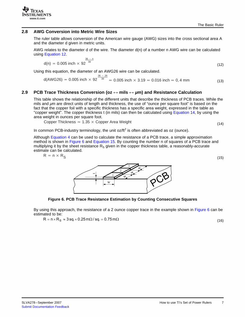
2.9 PCB Trace Thickness Conversion (oz ↔ mils ↔ μm) and Resistance Calculation
Copper Thickness 1.35 Copper Area Weight (14)
R n RS (15)
t
w
w
w
w
1
3
2
PCB
W=W´»´= m75.0.sq/m25.0.sq3RnR S (16)
The Basic Ruler
The ruler table allows conversion of the American wire gauge (AWG) sizes into the cross sectional area Aand the diameter d given in metric units.
AWG relates to the diameter d of the wire. The diameter d(n) of a number n AWG wire can be calculatedusing Equation 12.
Using this equation, the diameter of an AWG26 wire can be calculated.
This table shows the relationship of the different units that describe the thickness of PCB traces. While themils and μm are direct units of length and thickness, the use of “ounce per square foot” is based on thefact that the copper foil with a specific thickness has a specific area weight, expressed in the table as"copper weight". The copper thickness t (in mils) can then be calculated using Equation 14, by using thearea weight in ounces per square foot.
In common PCB-industry terminology, the unit oz/ft2 is often abbreviated as oz (ounce).
Although Equation 4 can be used to calculate the resistance of a PCB trace, a simple approximationmethod is shown in Figure 6 and Equation 15. By counting the number n of squares of a PCB trace andmultiplying it by the sheet resistance RS given in the copper thickness table, a reasonably-accurateestimate can be calculated.
Figure 6. PCB Trace Resistance Estimation by Counting Consecutive Squares
By using this approach, the resistance of a 2 ounce copper trace in the example shown in Figure 6 can beestimated to be:
SLVA278–September 2007 How to use TI’s Set of Power Rulers 7Submit Documentation Feedback
www.ti.com
3 The Voltage Regulator/Switching Converter Ruler
3.1 Calculation of Output Voltage Divider
R1R2
VOUTVREF
1 5 V1.25 V
1 3.(17)
W=W´-
=´-
= 800k1V8.0V8.1
V8.0R
VV
VR 1
REFOUT
REF
2
(18)
3.2 Calculation of Hold-Up Capacitance
The Voltage Regulator/Switching Converter Ruler
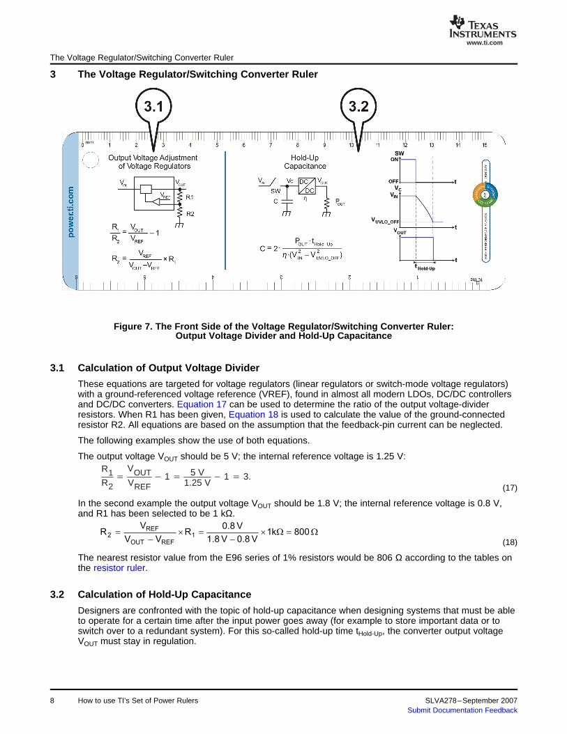
Figure 7. The Front Side of the Voltage Regulator/Switching Converter Ruler:Output Voltage Divider and Hold-Up Capacitance
These equations are targeted for voltage regulators (linear regulators or switch-mode voltage regulators)with a ground-referenced voltage reference (VREF), found in almost all modern LDOs, DC/DC controllersand DC/DC converters. Equation 17 can be used to determine the ratio of the output voltage-dividerresistors. When R1 has been given, Equation 18 is used to calculate the value of the ground-connectedresistor R2. All equations are based on the assumption that the feedback-pin current can be neglected.
The following examples show the use of both equations.
The output voltage VOUT should be 5 V; the internal reference voltage is 1.25 V:
In the second example the output voltage VOUT should be 1.8 V; the internal reference voltage is 0.8 V,and R1 has been selected to be 1 kΩ.
The nearest resistor value from the E96 series of 1% resistors would be 806 Ω according to the tables onthe resistor ruler.
Designers are confronted with the topic of hold-up capacitance when designing systems that must be ableto operate for a certain time after the input power goes away (for example to store important data or toswitch over to a redundant system). For this so-called hold-up time tHold-Up, the converter output voltageVOUT must stay in regulation.
8 How to use TI’s Set of Power Rulers SLVA278–September 2007Submit Documentation Feedback
www.ti.com
( ) [ ]F120
)V280()V370(%85
ms15W2002
VV
tP2C
222OFF_UVLO
2IN
UpHoldOUT
min m»-´
´´=
-´h
´´=
-
(19)
CMin_tol CMin
1 tolInitial 1 tolAging
120 F
(1 0.2) (1 0.2) 188 F.
(20)
The Voltage Regulator/Switching Converter Ruler
Off-line power supplies, applications of DC/DC converters in telecom/datacom, and embedded computersoften have this requirement. To operate the application during tHold-Up, the energy is taken from the inputbulk capacitor C of the converter. To be used in that way, a converter must be able to operate with amuch lower voltage at it’s input than the nominal input voltage VIN. This lower voltage is defined by theundervoltage lockout level; the point where the converter switches off (VUVLO_OFF).
The example shown in Equation 19 calculates the minimum required hold-up capacitance CMin for anoff-line power supply with a boost PFC in front of the DC/DC converter. The output capacitor of the boostPFC acts as the hold-up capacitor for the DC/DC converter in this case. When the mains voltage isavailable the capacitor voltage is regulated by the boost PFC to be within a range of 370 V–410 V. Itshould be furthermore assumed, that the DC/DC converter has an efficiency η of 85% and is required tooperate over a given hold-up time tHold-Up of 15 ms with an output power POUT of 200W. VUVLO_OFF of theDC/DC converter is set to 280 V.
Including the effects of initial tolerance tolInitial and aging tolAging, the final minimum required capacitanceCMin_tol can be calculated according to Equation 20 based on 20% initial tolerance and tolerance for agingof 20% too.
The table of preferred values for capacitors (section 4.1 on the capacitor / inductor ruler) gives 220 μF asthe next fitting capacitance value out of the E12 series.
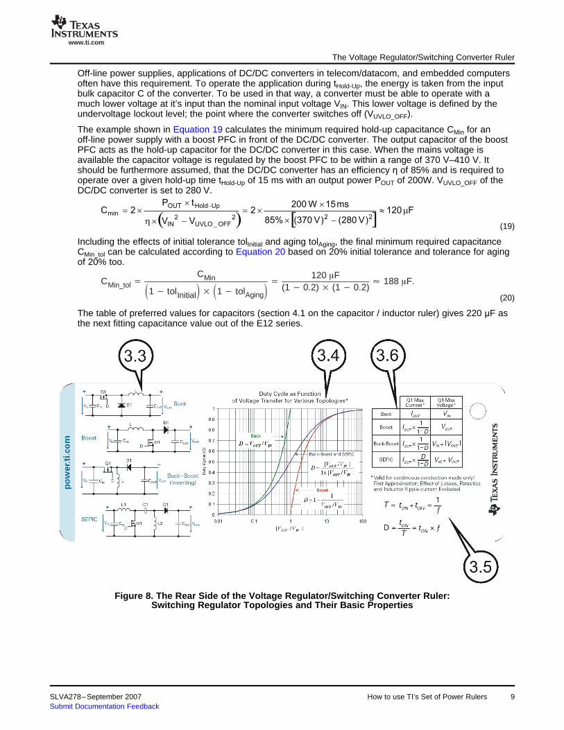
Figure 8. The Rear Side of the Voltage Regulator/Switching Converter Ruler:Switching Regulator Topologies and Their Basic Properties
SLVA278–September 2007 How to use TI’s Set of Power Rulers 9Submit Documentation Feedback

www.ti.com
3.3 Most Commonly Used Topologies for Non-Isolated Switching Regulators
3.4 Voltage Transfer Function for the Formerly Mentioned 4 Basic Topologies
3.5 Basic Time and Frequency Relation for PWM Based Circuits
T
tON
tOFF
T tON tOFF1ƒ (21)
DtONT tON ƒ
(22)
D1'D -= (23) TDtON ´= (24)
T'DT)D1(tOFF ´=´-= (25)
The Voltage Regulator/Switching Converter Ruler
The four figures show the basic topologies for the power stage of the following types of converters:
– Buck Converter (Step-Down) VOUT < VIN
– Boost Converter (Step-Up) VOUT > VIN
– Buck-Boost Converter (Inverting Step-Up/Down) VIN ≥ – VOUT ≥ VIN
– SEPIC Converter (Step-Up/Down) VIN ≥ VOUT ≥ VIN
All topologies are shown in a non-synchronous mode configuration, for their synchronous-modecounterparts the diode D1 is replaced by a second active switch.
The term Buck-Boost is inconsistently used in current technical literature. The initial meaning in reference[1] (See References) followed in this document is that VOUT can be higher (boost) or lower (buck) inmagnitude than VIN and that the polarity of VOUT is inverted with respect to the polarity of VIN. In contrast,the use of Buck-Boost is also found in relation to circuits not inverting the polarity. Reference [2] inReferences is an example. In addition to this, a SEPIC can do the same voltage conversion withoutchanging the polarity. SEPIC stands for Single-Ended Primary Inductance Converter.
This graph allows to convert a VOUT/VIN ratio directly into the required duty cycle of the DC/DC controlleror converter. This is especially helpful, when limits like maximum duty cycle DMax or minimum controllableON-time tON comes into place and in cases where the usability of a dedicated DC/DC controller/converterfor the application needs to be verified. The knowledge of the duty cycle is furthermore required forestimating the maximum drain current of Q1 as outlined in section 3.6.
The curves and the equations for the duty cycle are valid for the ideal and therefore loss-less case and forthe continuous conduction mode only! Especially under the condition of full output load, the practicalrequired duty cycle will be larger than that given for the ideal case.
This section shows how the duty cycle D, the switching frequency f, the switching period T and the timesduring which the switch Q1 (see section 3.3) is switched ON (ON-time tON) respectively OFF (OFF-timetOFF ) are related to each other.
Figure 9. The Duty Cycle D as the Ratio of the ON-Time tON to the Switching Period T
The basic relations are:
In addition to that, the following relations should be kept in mind:
How to use TI’s Set of Power Rulers10 SLVA278–September 2007Submit Documentation Feedback
www.ti.com
3.6 Current and Voltage Stress for the 4 Basic Topologies
4 The Capacitor/Inductor Ruler
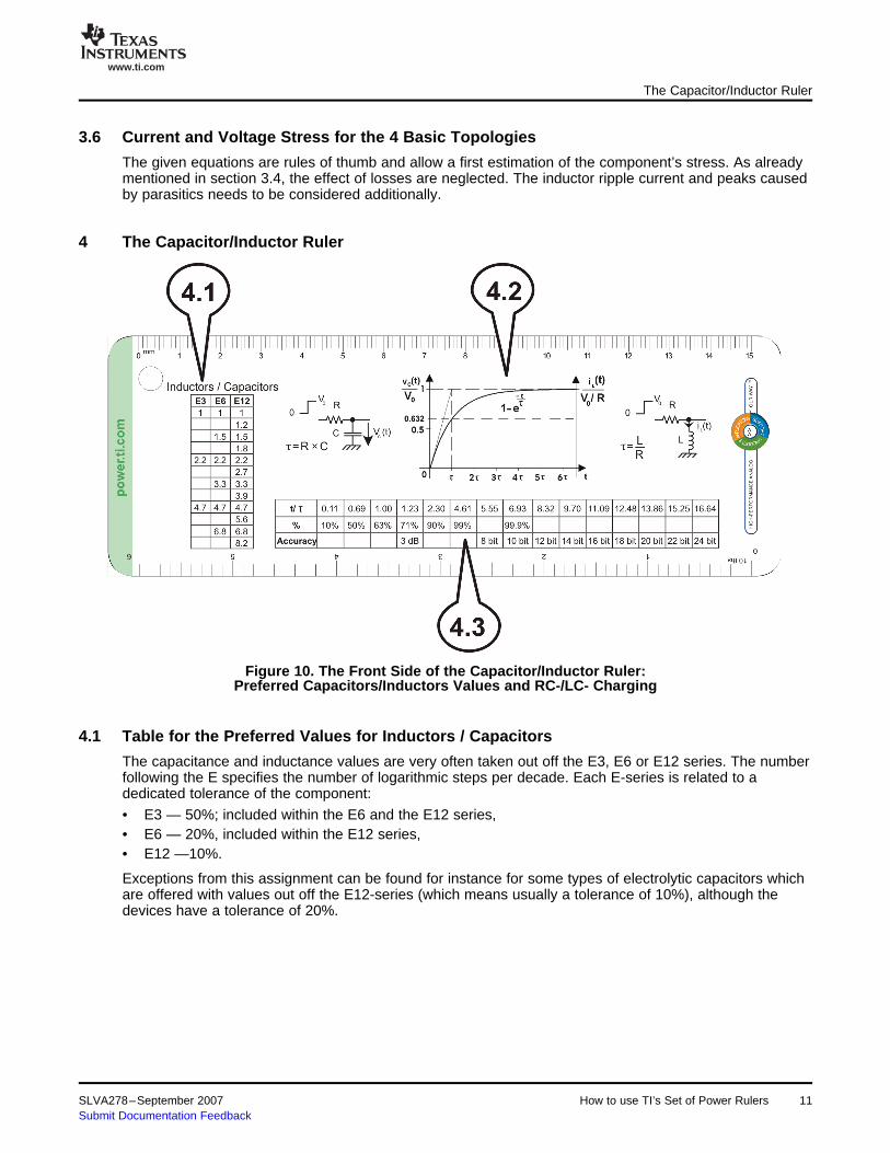
4.1 Table for the Preferred Values for Inductors / Capacitors
The Capacitor/Inductor Ruler
The given equations are rules of thumb and allow a first estimation of the component’s stress. As alreadymentioned in section 3.4, the effect of losses are neglected. The inductor ripple current and peaks causedby parasitics needs to be considered additionally.
Figure 10. The Front Side of the Capacitor/Inductor Ruler:Preferred Capacitors/Inductors Values and RC-/LC- Charging
The capacitance and inductance values are very often taken out off the E3, E6 or E12 series. The numberfollowing the E specifies the number of logarithmic steps per decade. Each E-series is related to adedicated tolerance of the component:
• E3 — 50%; included within the E6 and the E12 series,• E6 — 20%, included within the E12 series,• E12 —10%.
Exceptions from this assignment can be found for instance for some types of electrolytic capacitors whichare offered with values out off the E12-series (which means usually a tolerance of 10%), although thedevices have a tolerance of 20%.
SLVA278–September 2007 How to use TI’s Set of Power Rulers 11Submit Documentation Feedback
www.ti.com
4.2 Graph of Capacitor / Inductor Charge
•V0 for the capacitor charging, respectively to
•
V0R for the inductor charging.
4.3 Accuracy and Resolution for Capacitor/Inductor Charging
The Capacitor/Inductor Ruler
The graph represents the charging curves when applying a unit step function (from 0 to V0) to an RC-respectively an RL- circuit.
The maximum rate of change for the capacitor voltage vC(t) respectively for the inductor current IL(t)happens at the beginning of the charging cycle at t = 0 and equals to
The table lists the:
• Ratio (%) between the capacitor voltage vC(t) or inductor current IL(t) at a dedicated time t and theirmaximum achievable value at t = ∞.
• Accuracy (dB or bit) of vC(t) or IL(t) at a dedicated time t referred to their maximum achievable value att = ∞.
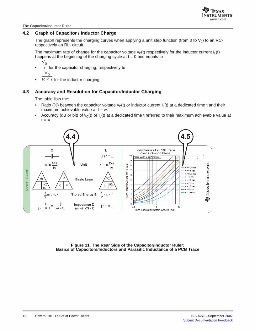
Figure 11. The Rear Side of the Capacitor/Inductor Ruler:Basics of Capacitors/Inductors and Parasitic Inductance of a PCB Trace
How to use TI’s Set of Power Rulers12 SLVA278–September 2007Submit Documentation Feedback

www.ti.com
4.4 Capacitors/Inductors: Symbol, Unit, Basic Laws and Equations
1 F 1 As1 V (26)
1 F 1 A s
1 V,
(27)
1 H 1 Vs1 A (28)
1 H1 V s
1 A (29)
4.5 Graph of PCB Trace Inductance
h
w
PCB
The Capacitor/Inductor Ruler
Especially the given units and basic laws help to remember the basic behavior of a capacitor and aninductor.
Equation 26 and Equation 27 allows for example to derive easily, how much the capacitor voltagechanges during a given time:
means simply that a constant current of 1 A applied to a capacitor with 1 F changes the capacitor voltageby 1 V in 1 s. Because this seems to be kind of unrealistic case, a better example can be achieved bymultiplying the left and the right side of the equation with μ:
representing now the same 1-V change, but based on applying 1 A to a capacitor of 1 μF for a time of 1μs.
The same way of using the unit of a device can be applied for inductors.
where Equation 29 can be translated into the fact that applying a constant voltage of 1V across aninductor of 1 μH over a time of 1 μs causes the inductor current to change by 1 A.
This graph should remind all designers dealing with fast changing voltages or currents, that each PCBtrace has a parasitic inductance associated to it. Switching regulators are a good example for this. While itis clear, that the power path where the large currents flow needs to be designed by keeping the rules ofminimizing parasitics, this is very often overlooked for parts of the circuit where no fast currents changesor no high currents are (expected). The connection of a MOSFET driver output to the gate of a MOSFETis a good example for this. Unwanted inductance can cause significant ringing and can slow-down theswitching of the MOSFET. The curves for the trace inductance per cm of trace length show, that thedifferences between thin and wide traces (w) as well as between ground planes placed near of far away(h) from the trace are significant.
Figure 12. PCB Trace Inductance Determined by the Width and Length of the Trace and it's Distance fromGround
There are a number of different methods for estimating/calculating trace inductance as outlined inreferences [3] and [4] (See References). They all are suffering from the fact that they are valid undercertain conditions only.
For the purpose of this document the 2D Field Solver software Si8000m/Si9000e from Polar Instruments(www.polarinstruments.com) was therefore used. The Si8000m provides an additional EXCEL-Interfacefor integration into an EXCEL Spreadsheet to simulate various geometry scenarios. Further backgroundinformation can be found in [5].
SLVA278–September 2007 How to use TI’s Set of Power Rulers 13Submit Documentation Feedback

www.ti.com
5 The Resistor Ruler
5.1 Table for the Preferred Values for Resistors
The Resistor Ruler
Figure 13. The Front Side of the Resistor Ruler: Preferred Resistor Values (1%–10%)
Standard resistor values are often taken from the E12, E24, E48 and E96 series. The number followingthe "E" specifies the number of logarithmic steps per decade. Each E-series is related to a dedicatedtolerance of the resistor:
• E12 — 10%; included within the E24 series,• E24 — 5%• E48 — 2%; included within the E96 series,• E96 — 1%
Figure 14. The Rear Side of the Resistor Ruler: Resistor’s Basics, Dimensions and Electrical Limits
14 How to use TI’s Set of Power Rulers SLVA278–September 2007Submit Documentation Feedback
www.ti.com
5.2 Resistors: Symbol, Unit, Basic Laws and Equations
5.3 Chip Resistors: Basic Data
5.4 MELF Resistors: Basic Data
6 References
References
The well-known basic Ohm’s Law and its derivatives are used to calculate the power P, when theresistance R and the voltage V respectively the current I are known.
The table lists the basic specification found for chip resistors as a starting point for design activities. Datasheets needs to be used for ultimate values.
• Type: related to inch-size
– The first two digits represent the length– The remaining digits stand for the width– 2-digit numbers are measured in hundredths of inch– 3-digit numbers are measured in thousands of inch (theoretical value)
• Dimensions: length and width given in mm
– Values are based on the maximum values found in Data sheets from different manufacturers• Power P: maximum power dissipation at an ambient temperature of 70°C
– Given values in the Data sheets of the manufacturers differ from case to case.• Max RCWV: maximum rated continuous working voltage
– Different values are found in different data sheets
• Type• Dimensions: length and diameter given in mm
– Values are based on the maximum values found in data sheets• Power and Max RCWV (See Section 5.3
1. Everett Rogers; Understanding Buck-Boost Power Stages in Switch Mode Power Supplies, TexasInstruments Application Report (SLVA059A) – November 2002
2. TPS63000/01/02 High Efficient Single Inductor BUCK-BOOST Converter with 1.8-A Switches, TexasInstruments Data sheet (SLVS520A) – April 2006
3. Robert Kollman, Constructing Your Power Supply – Layout Considerations, 2004-5 TI Unitrode DesignSeminar Series - SEM1600; Topic 4 (SLUP230)
4. Howard Johnson, Martin Graham, High-Speed Digital Design – A Handbook of Black Magic, PrenticeHall
5. http://www.polarinstruments.com/support/cits/cits_index.html
SLVA278–September 2007 How to use TI’s Set of Power Rulers 15Submit Documentation Feedback
IMPORTANT NOTICE
Texas Instruments Incorporated and its subsidiaries (TI) reserve the right to make corrections, modifications, enhancements,improvements, and other changes to its products and services at any time and to discontinue any product or service without notice.Customers should obtain the latest relevant information before placing orders and should verify that such information is current andcomplete. All products are sold subject to TI’s terms and conditions of sale supplied at the time of order acknowledgment.
TI warrants performance of its hardware products to the specifications applicable at the time of sale in accordance with TI’sstandard warranty. Testing and other quality control techniques are used to the extent TI deems necessary to support thiswarranty. Except where mandated by government requirements, testing of all parameters of each product is not necessarilyperformed.
TI assumes no liability for applications assistance or customer product design. Customers are responsible for their products andapplications using TI components. To minimize the risks associated with customer products and applications, customers shouldprovide adequate design and operating safeguards.
TI does not warrant or represent that any license, either express or implied, is granted under any TI patent right, copyright, maskwork right, or other TI intellectual property right relating to any combination, machine, or process in which TI products or servicesare used. Information published by TI regarding third-party products or services does not constitute a license from TI to use suchproducts or services or a warranty or endorsement thereof. Use of such information may require a license from a third party underthe patents or other intellectual property of the third party, or a license from TI under the patents or other intellectual property of TI.
Reproduction of TI information in TI data books or data sheets is permissible only if reproduction is without alteration and isaccompanied by all associated warranties, conditions, limitations, and notices. Reproduction of this information with alteration is anunfair and deceptive business practice. TI is not responsible or liable for such altered documentation. Information of third partiesmay be subject to additional restrictions.
Resale of TI products or services with statements different from or beyond the parameters stated by TI for that product or servicevoids all express and any implied warranties for the associated TI product or service and is an unfair and deceptive businesspractice. TI is not responsible or liable for any such statements.
TI products are not authorized for use in safety-critical applications (such as life support) where a failure of the TI product wouldreasonably be expected to cause severe personal injury or death, unless officers of the parties have executed an agreementspecifically governing such use. Buyers represent that they have all necessary expertise in the safety and regulatory ramificationsof their applications, and acknowledge and agree that they are solely responsible for all legal, regulatory and safety-relatedrequirements concerning their products and any use of TI products in such safety-critical applications, notwithstanding anyapplications-related information or support that may be provided by TI. Further, Buyers must fully indemnify TI and itsrepresentatives against any damages arising out of the use of TI products in such safety-critical applications.
TI products are neither designed nor intended for use in military/aerospace applications or environments unless the TI products arespecifically designated by TI as military-grade or "enhanced plastic." Only products designated by TI as military-grade meet militaryspecifications. Buyers acknowledge and agree that any such use of TI products which TI has not designated as military-grade issolely at the Buyer's risk, and that they are solely responsible for compliance with all legal and regulatory requirements inconnection with such use.
TI products are neither designed nor intended for use in automotive applications or environments unless the specific TI productsare designated by TI as compliant with ISO/TS 16949 requirements. Buyers acknowledge and agree that, if they use anynon-designated products in automotive applications, TI will not be responsible for any failure to meet such requirements.
Following are URLs where you can obtain information on other Texas Instruments products and application solutions:
Products Applications
Amplifiers amplifier.ti.com Audio www.ti.com/audio
Data Converters dataconverter.ti.com Automotive www.ti.com/automotive
DSP dsp.ti.com Broadband www.ti.com/broadband
Interface interface.ti.com Digital Control www.ti.com/digitalcontrol
Logic logic.ti.com Military www.ti.com/military
Power Mgmt power.ti.com Optical Networking www.ti.com/opticalnetwork
Microcontrollers microcontroller.ti.com Security www.ti.com/security
RFID www.ti-rfid.com Telephony www.ti.com/telephony
Low Power www.ti.com/lpw Video & Imaging www.ti.com/videoWireless
Wireless www.ti.com/wireless
Mailing Address: Texas Instruments, Post Office Box 655303, Dallas, Texas 75265Copyright © 2007, Texas Instruments Incorporated