Embed Size (px)
Citation preview
HTEE25608
High Temperature EEPROM 256Kb
The HTEE25608 is a 256 kbit asynchronous non-volatile memory for high temperature
applications. The HTEE25608 is configured as 512 x 64 page memory that has both an
8-bit parallel and a serial interface for ease of use. Utilizing Honeywell’s High Temperature
0.8 µm SOI CMOS process, it is designed for continuous operation at 225°C.
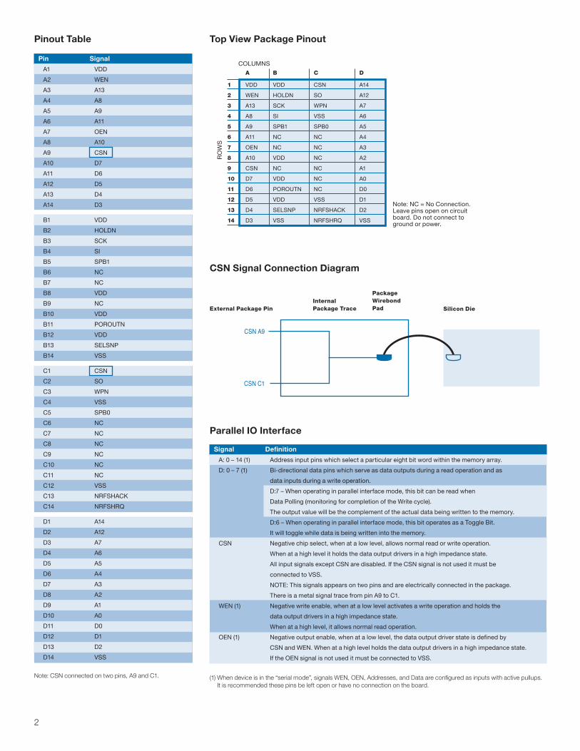
The HTEE25608 contains a 64 byte page write buffer for efficient data transfer. The page write operation allows 1 to 64 bytes to be written, providing the flexibility needed for any application. The write operation is simplified by on- chip latches and a self-timed write cycle, and status bits are provided to externally monitor the operation. An autonomous memory refresh capability is provided to extend data retention at extreme high-temperatures.
The memory contains integrated Error Coding Correction consisting of 56 Error-Correction Coding bits per page (64 bytes). The ECC corrects up to 8 bit errors per 64-byte page. Write protection control is provided to secure EEPROM data. This device is ideal for use as program and/or data memory in deep earth, avionics, nuclear and other extreme environment applications.
Functional Block Diagram
Features
n 256kb EEPROM
n Operating temperature range of -55°C to +225°C
n Single +5 V analog supply
n Serial and Parallel interface
n SPI serial communications
n Integrated high voltage supply
n Page and Byte write capability
n 64 byte Page Write Buffer
n Up to 10,000 program/erase cycle for each data bit
n Functionally similar to industry EEPROMs
n Hardware and Software Write Data Protection
n Fast Read Access: - At new page address: < 200 ns at 225°C
High Temp and Ruggedized Package The HTEE25608 is packaged in
a 56 lead ceramic Pin -grid Array (PGA) package.
ADDR [14:0]NRFSHRQ
NRFSHACKCSN
WENOEN
SELSNP
SBP1 SBP0 WPN HOLDN SCK
POROUTN
DATA [7:0]
SI SO
Status Registers
Digital Logic / Control
IO ControlBlock Protect SPI Control Logic
SPI
15
8
Address Decode ECCMemory Refresh and ControlTimerControl Logic
Data Buffer / 64 Byte Page Register
Data Polling and Toggle Bit
Data IO Buffer High Voltage SupplyMemory Array
512 x (512 + 56)POR
Pinout Table
2
Top View Package Pinout
Parallel IO Interface
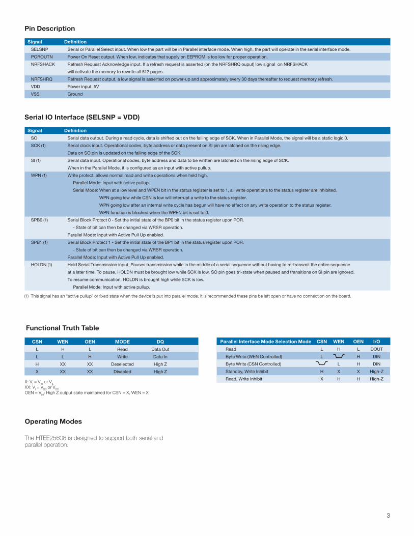
CSN Signal Connection Diagram
Signal DefinitionA: 0 – 14 (1) Address input pins which select a particular eight bit word within the memory array.D: 0 – 7 (1) Bi-directional data pins which serve as data outputs during a read operation and as data inputs during a write operation. D:7 – When operating in parallel interface mode, this bit can be read when Data Polling (monitoring for completion of the Write cycle). The output value will be the complement of the actual data being written to the memory. D:6 – When operating in parallel interface mode, this bit operates as a Toggle Bit. It will toggle while data is being written into the memory. CSN Negative chip select, when at a low level, allows normal read or write operation. When at a high level it holds the data output drivers in a high impedance state. All input signals except CSN are disabled. If the CSN signal is not used it must be connected to VSS. NOTE: This signals appears on two pins and are electrically connected in the package. There is a metal signal trace from pin A9 to C1. WEN (1) Negative write enable, when at a low level activates a write operation and holds the data output drivers in a high impedance state. When at a high level, it allows normal read operation. OEN (1) Negative output enable, when at a low level, the data output driver state is defined by CSN and WEN. When at a high level holds the data output drivers in a high impedance state. If the OEN signal is not used it must be connected to VSS.
Pin SignalA1 VDD A2 WEN A3 A13 A4 A8 A5 A9 A6 A11 A7 OEN A8 A10 A9 CSN A10 D7 A11 D6 A12 D5 A13 D4 A14 D3
B1 VDD B2 HOLDN B3 SCK B4 SI B5 SPB1 B6 NC B7 NC B8 VDD B9 NC B10 VDD B11 POROUTN B12 VDD B13 SELSNP B14 VSS
C1 CSN C2 SO C3 WPN C4 VSS C5 SPB0 C6 NC C7 NC C8 NC C9 NC C10 NC C11 NC C12 VSS C13 NRFSHACK C14 NRFSHRQ
D1 A14 D2 A12 D3 A7 D4 A6 D5 A5 D6 A4 D7 A3 D8 A2 D9 A1 D10 A0 D11 D0 D12 D1 D13 D2 D14 VSS
1 VDD VDD CSN A14
2 WEN HOLDN SO A12
3 A13 SCK WPN A7
4 A8 SI VSS A6
5 A9 SPB1 SPB0 A5
6 A11 NC NC A4
7 OEN NC NC A3
8 A10 VDD NC A2
9 CSN NC NC A1
10 D7 VDD NC A0
11 D6 POROUTN NC D0
12 D5 VDD VSS D1
13 D4 SELSNP NRFSHACK D2
14 D3 VSS NRFSHRQ VSS
A B C D
External Package PinInternalPackage Trace
PackageWirebondPad Silicon Die
Note: CSN connected on two pins, A9 and C1.
COLUMNS
Note: NC = No Connection. Leave pins open on circuit board. Do not connect to ground or power.
ROW
S
(1) When device is in the “serial mode”, signals WEN, OEN, Addresses, and Data are configured as inputs with active pullups. It is recommended these pins be left open or have no connection on the board.
CSN A9
CSN C1
Parallel Interface Mode Selection Mode CSN WEN OEN I/O Read L H L DOUT Byte Write (WEN Controlled) L H DIN Byte Write (CSN Controlled) L H DIN Standby, Write Inhibit H X X High-Z Read, Write Inhibit X H H High-Z
3
Pin Description
Serial IO Interface (SELSNP = VDD)
Signal DefinitionSELSNP Serial or Parallel Select input. When low the part will be in Parallel interface mode. When high, the part will operate in the serial interface mode. POROUTN Power On Reset output. When low, indicates that supply on EEPROM is too low for proper operation. NRFSHACK Refresh Request Acknowledge input. If a refresh request is asserted (on the NRFSHRQ ouput) low signal on NRFSHACK will activate the memory to rewrite all 512 pages. NRFSHRQ Refresh Request output, a low signal is asserted on power-up and approximately every 30 days thereafter to request memory refresh. VDD Power input, 5V VSS Ground
Signal DefinitionSO Serial data output. During a read cycle, data is shifted out on the falling edge of SCK. When in Parallel Mode, the signal will be a static logic 0. SCK (1) Serial clock input. Operational codes, byte address or data present on SI pin are latched on the rising edge. Data on SO pin is updated on the falling edge of the SCK. SI (1) Serial data input. Operational codes, byte address and data to be written are latched on the rising edge of SCK. When in the Parallel Mode, it is configured as an input with active pullup. WPN (1) Write protect, allows normal read and write operations when held high. Parallel Mode: Input with active pullup. Serial Mode: When at a low level and WPEN bit in the status register is set to 1, all write operations to the status register are inhibited.
WPN going low while CSN is low will interrupt a write to the status register. WPN going low after an internal write cycle has begun will have no effect on any write operation to the status register. WPN function is blocked when the WPEN bit is set to 0.
SPB0 (1) Serial Block Protect 0 - Set the initial state of the BP0 bit in the status register upon POR. - State of bit can then be changed via WRSR operation. Parallel Mode: Input with Active Pull Up enabled. SPB1 (1) Serial Block Protect 1 - Set the initial state of the BP1 bit in the status register upon POR. - State of bit can then be changed via WRSR operation. Parallel Mode: Input with Active Pull Up enabled. HOLDN (1) Hold Serial Transmission input, Pauses transmission while in the middle of a serial sequence without having to re-transmit the entire sequence
at a later time. To pause, HOLDN must be brought low while SCK is low. SO pin goes tri-state when paused and transitions on SI pin are ignored. To resume communication, HOLDN is brought high while SCK is low. Parallel Mode: Input with active pullup.
(1) This signal has an “active pullup” or fixed state when the device is put into parallel mode. It is recommended these pins be left open or have no connection on the board.
Functional Truth Table
CSN WEN OEN MODE DQ L H L Read Data Out L L H Write Data In H XX XX Deselected High Z X XX XX Disabled High Z
X: VI = VIH or VIL XX: VI = VSS or VDD OEN = VIH: High Z output state maintained for CSN = X, WEN = X
Operating Modes
The HTEE25608 is designed to support both serial and parallel operation.
Special Functions
Memory RefreshA memory-refresh function is employed to enable long-term data storage at 250°C. A memory refresh-request pin (NRFSHRQ) is asserted on power-up and approximately every 30 days thereafter to request memory refresh. If this signal is acknowledged via a refresh-acknowledge input signal (NRFSHACK), then the memory will re-write itself in 512 sequential page-write operations. The
refresh requires approximately 45 seconds to be completed. Note that this refresh is optional and may be ignored by the system. The initial power-on refresh request “expires” after approximately 20 seconds if it is not acknowledged. In addition, due to the page-mode writing scheme, writing to any byte within a page effectively refreshes the entire page.
4
(1) Stresses in excess of those listed above may result in immediate permanent damage to the device. These are stress ratings only, and operation at these levels is not implied. Frequent or extended exposure to absolute maximum conditions may affect device reliability.
(2) Voltage referenced to VSS. (3) EEPROM power dissipation internally and external driving of loads must not exceed this specification (4) Class 1 electrostatic discharge (ESD) input protection voltage per MIL-STD-883, Method 3015 (5) A write operation occurs anytime the high voltage circuitry is engaged in order to write or refresh the memory. A full refresh of the memory counts as 512 write cycles towards this limit. (6) A bit toggle is written state change on any memory bit. Any time a value is written to memory, in which that value already is resident does not count towards this limit (i.e. REFRESH).
Absolute Maximum Ratings (1) RatingsSymbol Parameter Min Max Units VDD Supply Voltage (2) -0.5 6.0 Volts VPIN Voltage on Any Pin (2) -0.5 VDD+0.5 Volts TSTORE Storage Temperature -65 250 °C IOUT Average Output Current 25 mA TSOLDER Soldering Temperature 270•5 °C•sec PD Package Power Dissipation (3) 2.5 W ØJC Package Thermal Resistance (56 PGA) (Junction to Case) 10.0 °C/W VPROT Electrostatic Discharge Protection Voltage 2000 V TJ Junction Temperature 250 °C Write Operations (5) 120E6 Operations Bit Toggles (6) 10E3 State changes
Recommended Operating Conditions (1)
(1) Voltage referenced to VSS.
DescriptionSymbol Parameter Min Typ Max Units
VDD Supply Voltage 4.75 5.0 5.25 Volts TC External Package Temperature -55 225 °C Temp Op Operating Temperature -55 225 °C VPIN Voltage on Any Pin -0.3 VDD+0.3 Volts
(1) Unless otherwise specified, specifications apply over the full VDD-VSS range from -55°C to 225°C, VDDA externally connected to VDD, VSSA externally connected to VSS.
DC Electrical Characteristics LimitsSymbol Parameter Conditions (1) Min Typ Max Units IDDSB VDD Standby Current Parallel 2 mA Serial 10 mA IDDOPW Dynamic Current, Write Parallel and Serial 50 mA IDDOPR Dynamic Current, Read Parallel 125 mA Serial 75 mA IOZ Output Tri-State Leakage Output High Impedance -10 +10 µA IIL Input Leakage Current Low Standard Input, Vin=0V -10 µA Pull Up Input, Vin=0V -300 µA IIH Input Leakage Current High Standard Input, Vin=5V +10 µA Pull Up Input, Vin=5V +10 µA VIH High Level Input Voltage Applies to digital I/O signals, VDD = 5.0V 3.375 Volts VIL Low Level Input Voltage Applies to digital I/O signals, VDD = 5.0V 1.375 Volts VOH High Level Output Voltage Sourcing 6mA 4.2 Volts VOL Low Level Output Voltage Sinking 6mA 0.45 Volts
5
(1) This parameter is tested during initial qualification only.(2) This signal appears on two pins that are electrically connected in the package.
(1) Retention based on allowing refresh to occur when requested. (2) Without memory refresh
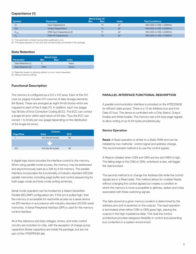
Capacitance (1) Worst Case (1)Symbol Parameter Min Max Units Test Conditions
CI Input Capacitance 14 pF VIN=VDD or VSS, f=500KHz CO Output Capacitance 14 pF VIN=VDD or VSS, f=500KHzCCSN CSN Input Capacitance (2) 17 pF VIN=VDD or VSS, f=500KHzCD Data I/O Capacitance 15 pF VIN=VDD or VSS, f=500KHz
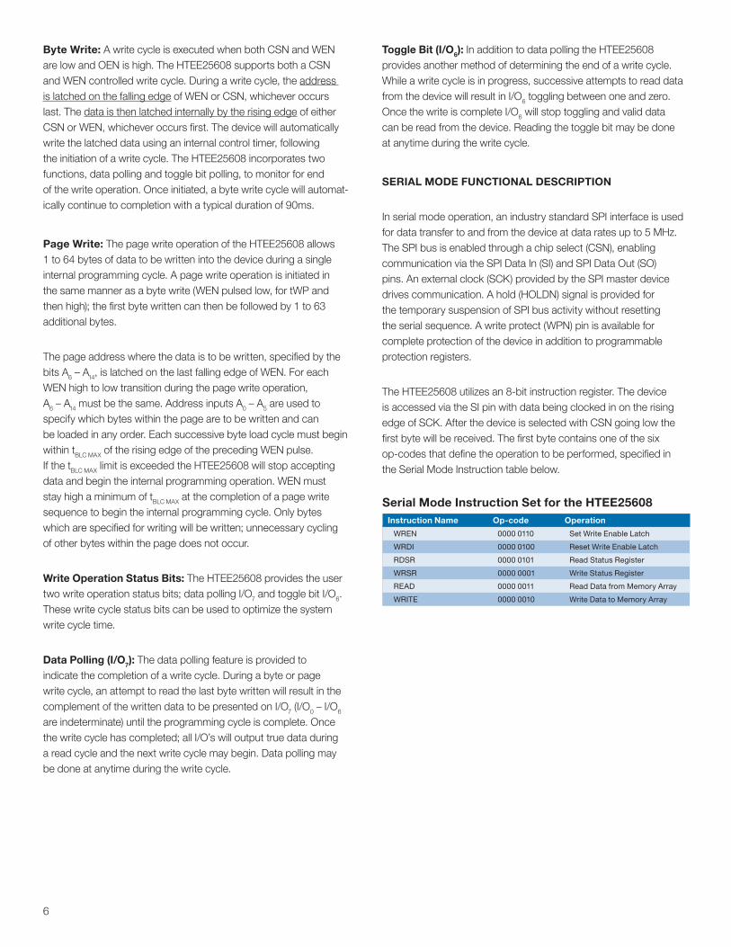
Data Retention Worst CaseParameter Min Max Units
Data Retention (1) 5 YearsData Retention (2) 1000 Hours
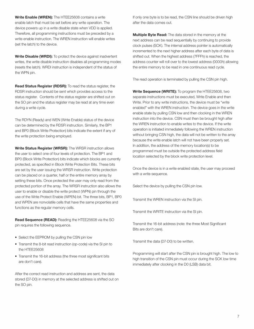
The memory is configured as a 512 x 512 array. Each of the 512 rows (or pages) includes 512 columns of data storage elements (64 Bytes). These are arranged as eight 64-bit blocks which are mapped to each of the 8 data I/O. In addition, each row (page) has 56 bits of Error Correction Coding (ECC). The ECC can correct a single-bit error within each block of 64-bits. Thus the ECC can correct 1 to 8 bits per row (page) depending on the distribution of the single-bit errors.
A digital logic block provides the interface control to the memory. When using parallel mode access, the memory may be addressed and asynchronously read as a 32K by 8-bit memory. The parallel interface incorporates the functionality of industry standard 28C256 parallel memories, including page buffer and control sequencing for both page-mode and byte-mode writing schemes.
Serial-mode operation can be invoked by a Select Serial/Not- Parallel (SELSNP) configuration pin. If this pin is pulled high, then the memory is accessible for read/write access as a serial device via SPI interface in accordance with industry standard 25C256 serial memories. A Serial Peripheral Interface (SPI) is used for the memory control interface.
All of the reference and bias voltages, timers, and write-control circuitry are included on-chip, with the exception of charge-pump capacitors (these capacitors are inside the package, but are not part of the HTEEPROM die).
PARALLEL INTERFACE FUNCTIONAL DESCRIPTION
A parallel communication interface is provided on the HTEE25608 for efficient data access. There is a 15 bit Address bus and 8 bit Data I/O bus. The device is controlled with a Chip Select, Output Enable and Write Enable. The memory has a 64-byte page register to allow writing of up to 64 bytes simultaneously.
Device Operation
Read: A Read operation is similar to a Static RAM and can be initiated by two methods; control signal and address change. The recommended method is to use the control signals.
A Read is initiated when CSN and OEN are low and WEN is high. The falling edge of the CSN or OEN, whichever is last, will trigger the read process.
The second method is to change the Address bits while the control signals are in a Read state. This method allows for multiple Reads without changing the control signals but creates a condition in which the memory is more susceptible to glitches, spikes and noise associated with these switching signals.
The data stored at a given memory location is determined by the address pins and is asserted on the outputs. The read operation is terminated when either CSN or OEN goes high, placing the outputs in the high impedance state. This dual line control architecture provides designers flexibility in control and preventing bus contention in a system environment.
Functional Description
ColumnPage/Row Data ECC
1 512 bits (64 bytes) 56
512 512 bits (64 bytes) 56
6
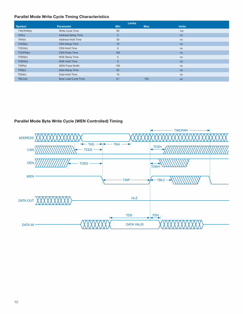
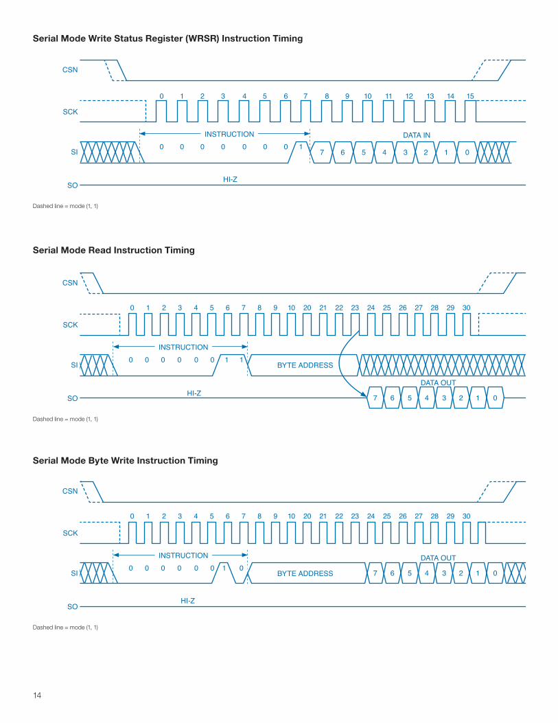
Byte Write: A write cycle is executed when both CSN and WEN are low and OEN is high. The HTEE25608 supports both a CSN and WEN controlled write cycle. During a write cycle, the address is latched on the falling edge of WEN or CSN, whichever occurs last. The data is then latched internally by the rising edge of either CSN or WEN, whichever occurs first. The device will automatically write the latched data using an internal control timer, following the initiation of a write cycle. The HTEE25608 incorporates two functions, data polling and toggle bit polling, to monitor for end of the write operation. Once initiated, a byte write cycle will automat-ically continue to completion with a typical duration of 90ms.
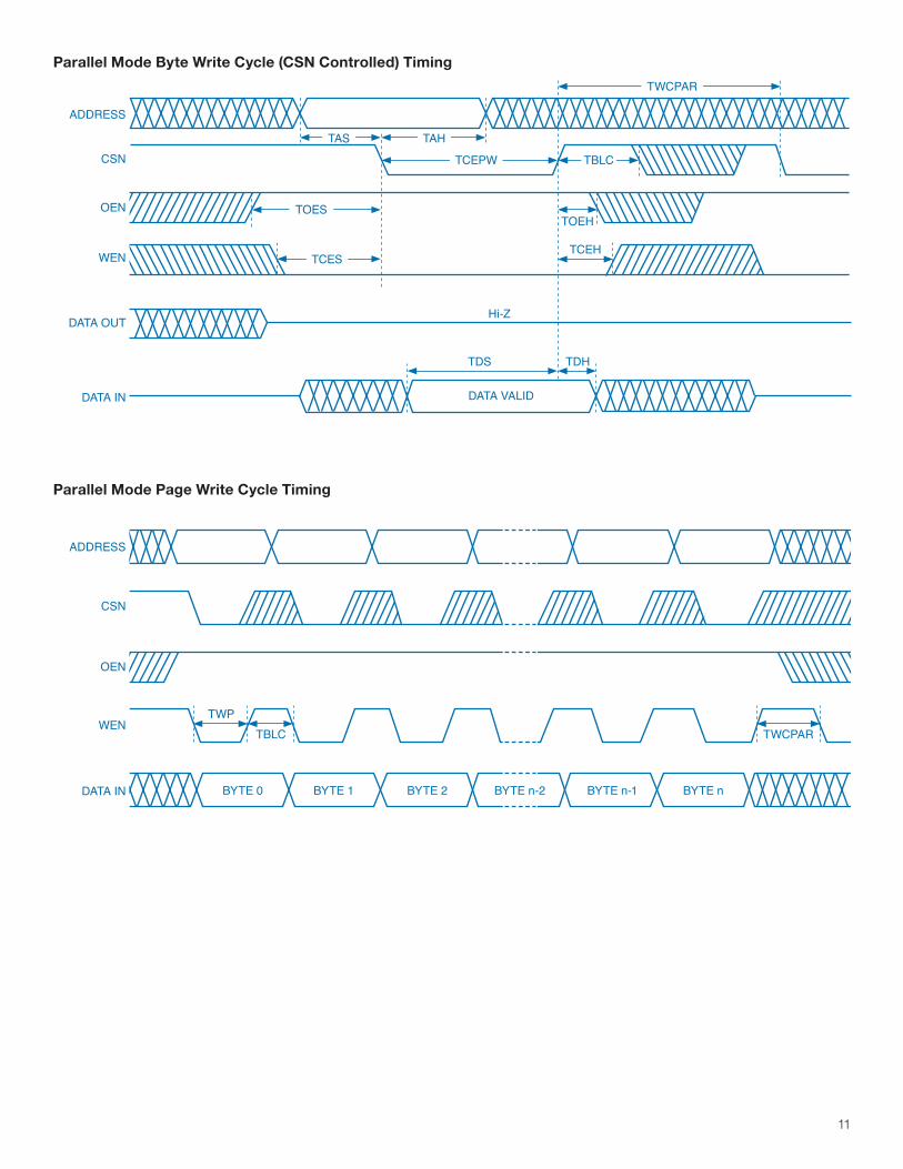
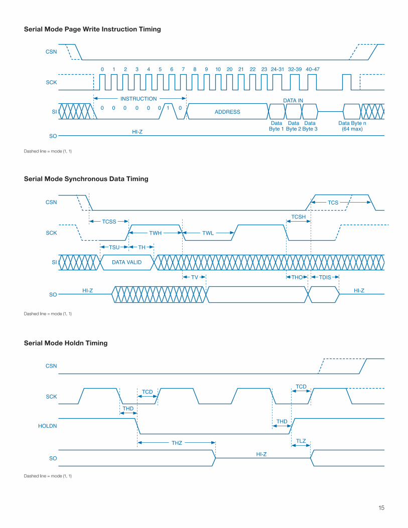
Page Write: The page write operation of the HTEE25608 allows 1 to 64 bytes of data to be written into the device during a single internal programming cycle. A page write operation is initiated in the same manner as a byte write (WEN pulsed low, for tWP and then high); the first byte written can then be followed by 1 to 63 additional bytes.
The page address where the data is to be written, specified by the bits A6 – A14, is latched on the last falling edge of WEN. For each WEN high to low transition during the page write operation, A6 – A14 must be the same. Address inputs A0 – A5 are used to specify which bytes within the page are to be written and can be loaded in any order. Each successive byte load cycle must begin within tBLC MAX of the rising edge of the preceding WEN pulse. If the tBLC MAX limit is exceeded the HTEE25608 will stop accepting data and begin the internal programming operation. WEN must stay high a minimum of tBLC MAX at the completion of a page write sequence to begin the internal programming cycle. Only bytes which are specified for writing will be written; unnecessary cycling of other bytes within the page does not occur.
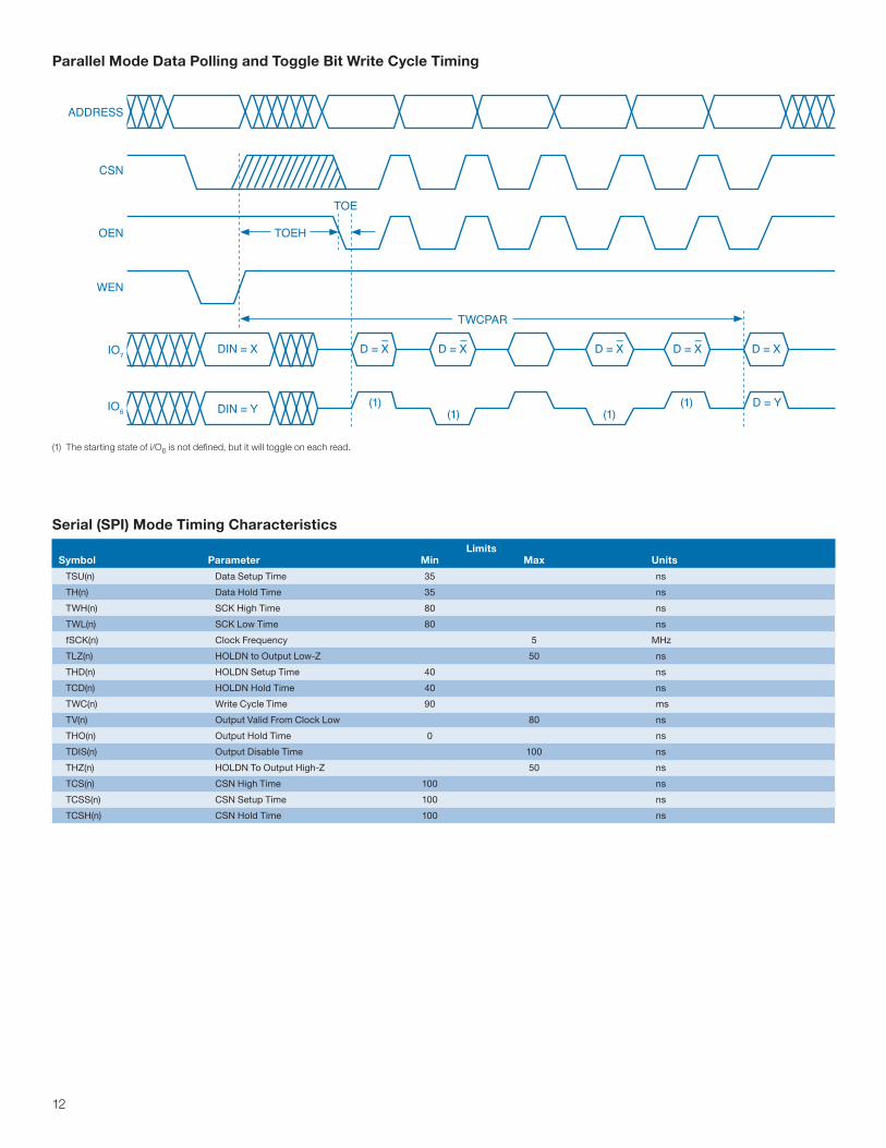
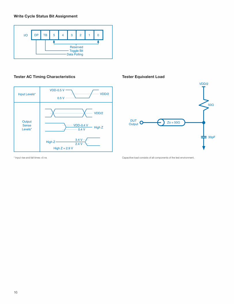
Write Operation Status Bits: The HTEE25608 provides the user two write operation status bits; data polling I/O7 and toggle bit I/O6. These write cycle status bits can be used to optimize the system write cycle time.
Data Polling (I/O7): The data polling feature is provided to indicate the completion of a write cycle. During a byte or page write cycle, an attempt to read the last byte written will result in the complement of the written data to be presented on I/O7 (I/O0 – I/O6 are indeterminate) until the programming cycle is complete. Once the write cycle has completed; all I/O’s will output true data during a read cycle and the next write cycle may begin. Data polling may be done at anytime during the write cycle.
Toggle Bit (I/O6): In addition to data polling the HTEE25608 provides another method of determining the end of a write cycle. While a write cycle is in progress, successive attempts to read data from the device will result in I/O6 toggling between one and zero. Once the write is complete I/O6 will stop toggling and valid data can be read from the device. Reading the toggle bit may be done at anytime during the write cycle.
SERIAL MODE FUNCTIONAL DESCRIPTION
In serial mode operation, an industry standard SPI interface is used for data transfer to and from the device at data rates up to 5 MHz. The SPI bus is enabled through a chip select (CSN), enabling communication via the SPI Data In (SI) and SPI Data Out (SO) pins. An external clock (SCK) provided by the SPI master device drives communication. A hold (HOLDN) signal is provided for the temporary suspension of SPI bus activity without resetting the serial sequence. A write protect (WPN) pin is available for complete protection of the device in addition to programmable protection registers.
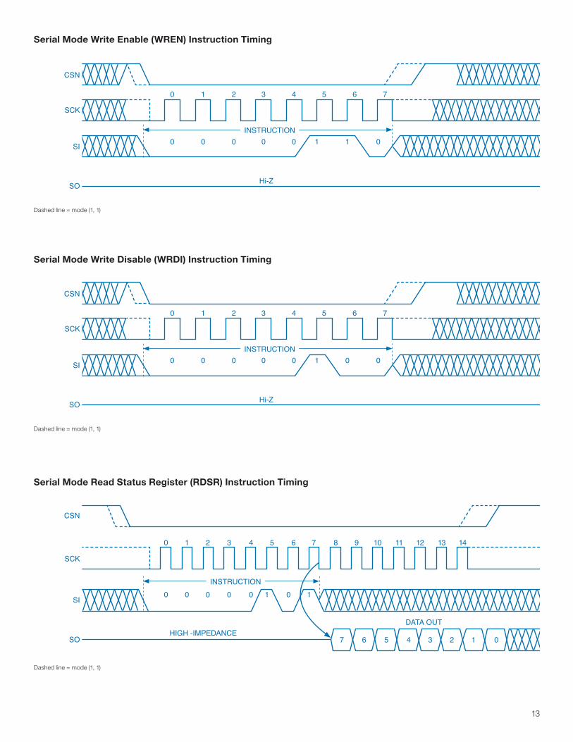
The HTEE25608 utilizes an 8-bit instruction register. The device is accessed via the SI pin with data being clocked in on the rising edge of SCK. After the device is selected with CSN going low the first byte will be received. The first byte contains one of the six op-codes that define the operation to be performed, specified in the Serial Mode Instruction table below.
Serial Mode Instruction Set for the HTEE25608Instruction Name Op-code Operation
WREN 0000 0110 Set Write Enable Latch WRDI 0000 0100 Reset Write Enable Latch RDSR 0000 0101 Read Status Register WRSR 0000 0001 Write Status RegisterREAD 0000 0011 Read Data from Memory Array WRITE 0000 0010 Write Data to Memory Array
7
Write Enable (WREN): The HTEE25608 contains a write enable latch that must be set before any write operation. The device powers up in a write disable state when VDD is applied. Therefore, all programming instructions must be preceded by a write enable instruction. The WREN instruction will enable writes (set the latch) to the device.
Write Disable (WRDI): To protect the device against inadvertent writes, the write disable instruction disables all programming modes (resets the latch). WRDI instruction is independent of the status of the WPN pin.
Read Status Register (RDSR): To read the status register, the RDSR instruction should be sent which provides access to the status register. Contents of the status register are shifted out on the SO pin and the status register may be read at any time even during a write cycle.
The RDYN (Ready) and WEN (Write Enable) status of the device can be determined by the RDSR instruction. Similarly, the BP1 and BP0 (Block Write Protection) bits indicate the extent if any of the write protection being employed.
Write Status Register (WRSR): The WRSR instruction allows the user to select one of four levels of protection. The BP1 and BP0 (Block Write Protection) bits indicate which blocks are currently protected, as specified in Block Write Protection Bits. These bits are set by the user issuing the WRSR instruction. Write protection can be placed on a quarter, half or the entire memory array by setting these bits. Once protected the user may only read from the protected portion of the array. The WRSR instruction also allows the user to enable or disable the write protect (WPN) pin through the use of the Write Protect Enable (WPEN) bit. The three bits, BP1, BP0 and WPEN are nonvolatile cells that have the same properties and functions as the regular memory cells.
Read Sequence (READ): Reading the HTEE25608 via the SO pin requires the following sequence.
• Select the EEPROM by pulling the CSN pin low
• Transmit the 8-bit read instruction (op-code) via the SI pin to the HTEE25608
• Transmit the 16-bit address (the three most significant bits are don’t care).
After the correct read instruction and address are sent, the data stored (D7-D0) in memory at the selected address is shifted out on the SO pin.
If only one byte is to be read, the CSN line should be driven high after the data comes out.
Multiple Byte Read: The data stored in the memory at the next address can be read sequentially by continuing to provide clock pulses (SCK). The internal address pointer is automatically incremented to the next higher address after each byte of data is shifted out. When the highest address (7FFFh) is reached, the address counter will roll over to the lowest address (0000h) allowing the entire memory to be read in one continuous read cycle.
The read operation is terminated by pulling the CSN pin high.
Write Sequence (WRITE): To program the HTEE25608, two separate instructions must be executed, Write Enable and then Write. Prior to any write instructions, the device must be “write enabled” with the WREN instruction. The device goes in the write enable state by pulling CSN low and then clocking in the WREN instruction into the device. CSN must then be brought high after the WREN instruction to enable writes to the device. If the write operation is initiated immediately following the WREN instruction without bringing CSN high, the data will not be written to the array because the write enable latch will not have been properly set. In addition, the address of the memory location(s) to be programmed must be outside the protected address field location selected by the block write protection level.
Once the device is in a write enabled state, the user may proceed with a write sequence.
Select the device by pulling the CSN pin low.
Transmit the WREN instruction via the SI pin.
Transmit the WRITE instruction via the SI pin.
Transmit the 16-bit address (note: the three Most Significant Bits are don’t care).
Transmit the data (D7-D0) to be written.
Programming will start after the CSN pin is brought high. The low to high transition of the CSN pin must occur during the SCK low time immediately after clocking in the D0 (LSB) data bit.
During an internal write cycle, all commands will be ignored except the RDSR instruction. The user can execute the RDSR instruction and read the status register to determine if the write cycle is still in progress. If Bit 0 (RDYN) = 1, the write cycle is still in progress. If RDYN = 0, the write cycle has ended and the device is ready for the next instruction.
64-byte Page Write: The HTEE25608 is capable of a 64-byte page write operation. After the first byte is written, the host may continue to write up to 64 bytes of data to the device. After each byte of data is received, the six lower order address bits are inter-nally incremented by one; the high order bits of the address will remain constant (the 64 bytes must reside on the same page). If more than 64 bytes of data are transmitted, the address counter will roll over and the previously written data will be overwritten. More specifically, if the address counter reaches the end of the page and the clock continues, the counter will roll over to the first address of the page and overwrite any data that may have been written. The HTEE25608 is automatically returned to the write dis-able state at the completion of the write cycle.
STATUS REGISTER
The Status Register indicates the status of the device; see Status Register Format for details on the status register format and Read Status Register Bit Definition for read status register bit definitions.
The RDYN (Ready): The bit indicates whether the HTEE25608 is busy with a write operation or is ready for new instructions. When set to 1 a write cycle is in progress and when set to 0 the device indicates it is ready for new instructions.
WEL (Write Enable Latch) - This bit indicates the status of the write enable latch and is read-only. When set to a 1, the latch allows writes to the array (write enable state), when set to a 0, the latch prohibits writes to the array (write disable state). The WEL bit can only be set by the WREN instruction and can be reset by the WRDI instruction.
WPEN (Write Protect Enable): This bit is an enable bit for the WPN pin. The WPN pin and WPEN bit in the status register control the programmable hardware write protect feature, see Write Protect Enable (WPEN) Operation.
Hardware write protection is enabled when the WPN pin is low and the WPEN bit is 1.
Hardware write protection is disabled when either the WPN pin is high or the WPEN bit is 0.
When the device is hardware write protected; writes to the status register including the block protect bits (BP1 and BP0), WPEN bit and the block protected sections in the memory array are disabled. Only the sections of the memory array that are not block protected can be written.
Block Protection (BP1 and BP0): These bits indicate which blocks are currently write-protected. These bits are set by the user issuing the WRSR instruction. The user is allowed to protect quarter of the memory, half of the memory or the entire memory by setting these bits. Once protected the user may only read from the protected portion of the array.
8
Status Register Format
Write Protect Enable (WPEN) Operation
Block Write Protection Bits
ReadStatusRegisterBitDefinition
BIT 7 BIT 6 BIT 5 BIT 4 BIT 3 BIT 2 BIT 1 BIT 0 WPEN X X X BP1 BP0 WEL RDYN
WPN WEL Protected Unprotected StatusWPEN Blocks Blocks Register 0 X 0 Protected Protected Protected 0 X 1 Protected Writable Writable 1 Low 0 Protected Protected Protected 1 Low 1 Protected Writable Protected X High 0 Protected Protected Protected X High 1 Protected Writable Writable
Array Protection Status Register Bits Array Address Level BP1 BP0 Protected No Protection 0 0 None Quarter 0 1 6000-7FFF Half 1 0 4000-7FFF Full 1 1 0000-7FFF
Bit Definition Bit 0 (RDYN) Set to 0 (RDYN) indicates the device is ready. Set to 1 indicates a write cycle is in progress. Bit 1 (WEL) Set to 0 indicates the device is not write enabled. Set to 1 indicates the device is write enabled. Bit 2 (BP0) See Block Write Protection Bits table Bit 3 (BP1) See Block Write Protection Bits table Bits 4 – 6 Are 0s when the device is not in an internal write cycle. Bit 7 (WPEN) See Write Protect Enable (WPEN) Operation table Bits 1 - 7 Are 0s during an internal write cycle
• Required every 1000 hours to retain data at maximum operating temperature
• Refresh request (NRFSHREQ) indicator is asserted every 30 days +/- 30% of continuous powered operation
• Refresh request (NRFSHREQ) indicator is also asserted on Power Up, and stays active for 20 +/- 30% seconds.
• Approximately 45 seconds is required to refresh the entire memory.
Memory Refresh
9
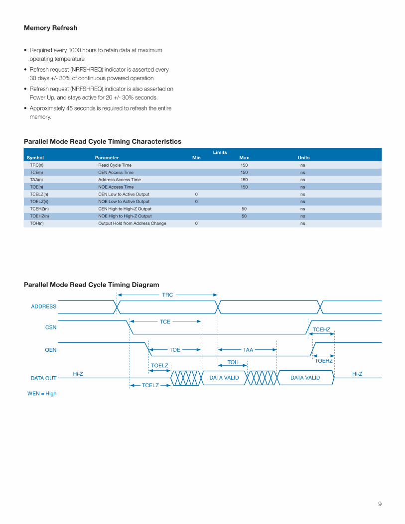
Parallel Mode Read Cycle Timing Diagram
Parallel Mode Read Cycle Timing Characteristics LimitsSymbol Parameter Min Max Units
TRC(n) Read Cycle Time 150 ns TCE(n) CEN Access Time 150 ns TAA(n) Address Access Time 150 ns TOE(n) NOE Access Time 150 ns TCELZ(n) CEN Low to Active Output 0 ns TOELZ(n) NOE Low to Active Output 0 ns TCEHZ(n) CEN High to High-Z Output 50 ns TOEHZ(n) NOE High to High-Z Output 50 ns TOH(n) Output Hold from Address Change 0 ns
WEN = High
DATA OUTHi-Z Hi-Z
OEN
CSN
ADDRESS
DATA VALID DATA VALIDTCELZ
TOELZ
TOE
TCE
TRC
TOH
TAA
TCEHZ
TOEHZ
10
Parallel Mode Write Cycle Timing Characteristics
Parallel Mode Byte Write Cycle (WEN Controlled) Timing
LimitsSymbol Parameter Min Max Units
TWCPAR(n) Write Cycle Time 90 ms TASn) Address Setup Time 0 ns TAH(n) Address Hold Time 50 ns TCES(n) CEN Setup Time 10 ns TCEH(n) CEN Hold Time 0 ns TCEPW(n) CEN Pulse Time 100 ns TOES(n) NOE Setup Time 5 ns TOEH(n) NOE Hold Time 0 ns TWP(n) WEN Pulse Width 100 ns TDS(n) Data Setup Time 50 ns TDH(n) Data Hold Time 10 ns TBLC(n) Byte Load Cycle Time 0.1 100 µs
Hi-Z
TOES
TWP TBLC
TASTCES
TAH
TWCPAR
TDS TDH
TCEH
TOEH
DATA VALID
WEN
DATA OUT
DATA IN
OEN
CSN
ADDRESS
11
Parallel Mode Byte Write Cycle (CSN Controlled) Timing
Parallel Mode Page Write Cycle Timing
OEN
CSN
ADDRESS
Hi-Z
TOES
TBLCTCEPW
TAS
TCES
TAH
TWCPAR
TDS
TWP
TDH
TBLC TWCPAR
BYTE 0 BYTE 1 BYTE 2 BYTE n-1 BYTE n
TCEH
TOEH
DATA VALID
WEN
DATA OUT
DATA IN
DATA IN
OEN
CSN
ADDRESS
WEN
BYTE n-2
12
Serial (SPI) Mode Timing Characteristics LimitsSymbol Parameter Min Max Units
TSU(n) Data Setup Time 35 ns TH(n) Data Hold Time 35 ns TWH(n) SCK High Time 80 ns TWL(n) SCK Low Time 80 ns fSCK(n) Clock Frequency 5 MHz TLZ(n) HOLDN to Output Low-Z 50 ns THD(n) HOLDN Setup Time 40 ns TCD(n) HOLDN Hold Time 40 ns TWC(n) Write Cycle Time 90 ms TV(n) Output Valid From Clock Low 80 ns THO(n) Output Hold Time 0 ns TDIS(n) Output Disable Time 100 ns THZ(n) HOLDN To Output High-Z 50 ns TCS(n) CSN High Time 100 ns TCSS(n) CSN Setup Time 100 ns TCSH(n) CSN Hold Time 100 ns
Parallel Mode Data Polling and Toggle Bit Write Cycle Timing
(1) The starting state of i/O6 is not defined, but it will toggle on each read.
TOEH
TWCPAR
DIN = X D = X– – – –
D = X D = X D = X D = X
DIN = Y (1) (1) D = Y(1) (1)
TOE
IO7
IO6
OEN
CSN
ADDRESS
WEN
13
Serial Mode Read Status Register (RDSR) Instruction Timing
Serial Mode Write Disable (WRDI) Instruction Timing
Serial Mode Write Enable (WREN) Instruction Timing
Dashed line = mode (1, 1)
Dashed line = mode (1, 1)
Dashed line = mode (1, 1)
INSTRUCTION
INSTRUCTION
INSTRUCTION
0
0
1
1
2
2
3
3
4
4
5
5
6
6
7
7
0
0
0
0
01234567
0
0
1
0
0
0
2
0
3
0
4
0
5
1 1
6
0
7 8 9 10 11 12 13 14
0
0
0
0
1
1
1
0
0
0
SCK
SCK
SI
SI
CSN
CSN
SO
SO Hi-Z
HIGH -IMPEDANCEDATA OUT
SCK
SI
SO
CSN
Hi-Z
14
Serial Mode Byte Write Instruction Timing
Serial Mode Write Status Register (WRSR) Instruction Timing
Serial Mode Read Instruction Timing
Dashed line = mode (1, 1)
Dashed line = mode (1, 1)
Dashed line = mode (1, 1)
INSTRUCTION
INSTRUCTION
INSTRUCTION
BYTE ADDRESS
BYTE ADDRESS
0
001234567
0
0
1
1
2
2
3
3
4
4
5
5
6
6
7
7
1
0
2
0
3
0
4
0
5
0 1
6
0
7
0
0
0
0
0
0
0
0
0
0
0
0
1
1
1
0
8 9 10 11 12 13 14 15
HI-Z
HI-Z
HI-Z
DATA IN
DATA OUT
DATA OUT
SCK
SI
SO
CSN
SCK
SCK
SI
SI
SO
SO
CSN
CSN
2 3 4 5 6 7 8 9 10 20 21 22 23 24 25 26 27 28 29 30 0 1
2 3 4 5 6 7 8 9 10 20 21 22 23 24 25 26 27 28 29 30 0 1
15
Serial Mode Page Write Instruction Timing
Serial Mode Holdn Timing
Serial Mode Synchronous Data Timing
Dashed line = mode (1, 1)
INSTRUCTION
ADDRESS0 0 0 0 0 0 1 0
HI-Z
DATA IN
24-31 32-39 40-47
DataByte 1
Data Byte n(64 max)
DataByte 2
DataByte 3
SCK
SI
SO
CSN
Dashed line = mode (1, 1)
Dashed line = mode (1, 1)
TWLTWH
THZ
TSU TH
TV THO TDIS
TCSSTCSH
TLZ
THD
THD
TCDTCD
TCS
HI-Z
HI-Z
HI-Z
DATA VALID
SCK
SI
CSN
SO
SCK
HOLDN
CSN
SO
0 1 2 3 4 5 6 7 8 9 10 20 21 22 23
16
Write Cycle Status Bit Assignment
Tester AC Timing Characteristics Tester Equivalent Load
* Input rise and fall times <5 ns Capacitive load consists of all components of the test environment.
DP TB 5 4 3 2 1 0I/O
ReservedToggle Bit
Data Polling
Input Levels*
Output Sense Levels*
VDD-0.5 V
VDD-0.4 V
VDD/2
VDD/2
High Z
High Z
High Z = 2.9 V
0.5 V
0.4 V
3.4 V2.4 V
DUT Output
VDD/2
30pF
50Ω
Zo = 50Ω
Reliability
Honeywell understands the stringent reliability requirements that high temperature systems require and has extensive experience in reliability testing on programs of this nature. Reliability attributes of the SOI process were characterized by testing specially designed
structures to evaluate failure mechanisms including hot carriers, electro-migration, and time-dependent dielectric breakdown. The results are fed back to improve the process to ensure the highest reliability products.
17
e1
Øb x561.27±.13 x4
A
B
C
14 13 12 11 10 9 8 7 6 5 4 3 2 1
D
D D1
E1
e2
AA2
.15A1
Q
(.20) x4
17.86Lid Flange
E 14.07Lid Step
36.91Lid Flange
33.63Lid Step
A-1 Indicator
Ø1.90 x56(C.30) x4
3
22
Millimeters InchesDimensions Min Nom Max Min Nom Max
A 9.69 10.28 10.86 .381 .405 .428A1 2.74 3.04 3.34 .108 .120 .131A2 4.49 4.95 5.40 .177 .195 .213b 0.41 0.46 0.51 .016 .018 .020D 37.72 38.10 38.48 1.485 1.500 1.515E 18.86 19.05 19.24 .743 .750 .757D1 32.69 33.02 33.35 1.287 1.300 1.313E1 15.09 15.24 15.39 .594 .600 .606e1 2.41 2.54 2.67 .095 .100 .105e2 4.95 5.08 5.21 .195 .200 .205Q 1.14 1.27 1.40 .045 .050 .055N 56
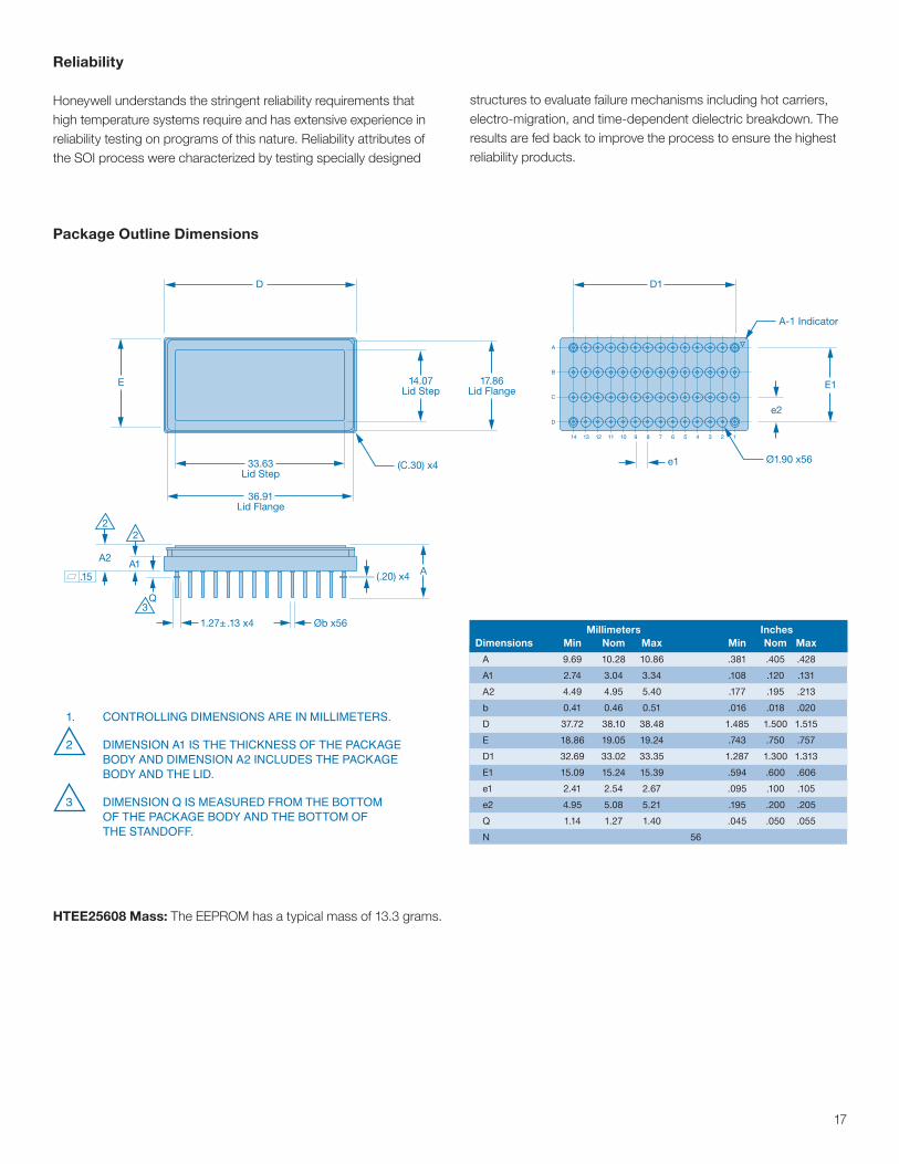
1. CONTROLLING DIMENSIONS ARE IN MILLIMETERS.
2 DIMENSION A1 IS THE THICKNESS OF THE PACKAGE BODY AND DIMENSION A2 INCLUDES THE PACKAGE BODY AND THE LID.
3 DIMENSION Q IS MEASURED FROM THE BOTTOM OF THE PACKAGE BODY AND THE BOTTOM OF THE STANDOFF.
Package Outline Dimensions
HTEE25608 Mass: The EEPROM has a typical mass of 13.3 grams.

Ordering Information
ProcessT = Hi Temp SOI
Description25608 = 256k,8bit wide bus
SourceH = Honeywell
PackageD = 56 Lead PGA
Honeywell AerospaceHoneywell12001 Highway 55Plymouth, MN 55441Telephone: 1.800.323.8295www.hightempsolutions.com
Form # ADS-14232May 2013© 2013 Honeywell International Inc.
Find out moreFor more information on Honeywell’s High Temperature Electronics visit us online at http://www.hightempsolutions.com/, or contact us at 800-323-8295 or 763-954-2474. Customer Service Email: [email protected].
Honeywell reserves the right to make changes to any products or technology herein to improve reliability, function or design. Honeywell does not assume any liability arising out of the application or use of any product or circuit described herein; neither does it convey any license under its patent rights nor the rights of others.
H T EE 25608 DPart Type
EE = Electrically Erasable PROM


![Motorola Eeprom[1]](https://img.pdfslide.net/doc/110x75/557201314979599169a0fa23/motorola-eeprom1.jpg)