Embed Size (px)
Citation preview
HUAWEI MU609 HSPA Mini PCIe Module
Hardware Guide
Issue 05
Date 2016-12-12
Copyright © Huawei Technologies Co., Ltd. 2016. All rights reserved.
No part of this manual may be reproduced or transmitted in any form or by any means without prior written
consent of Huawei Technologies Co., Ltd. and its affiliates ("Huawei").
The product described in this manual may include copyrighted software of Huawei and possible licensors.
Customers shall not in any manner reproduce, distribute, modify, decompile, disassemble, decrypt, extract,
reverse engineer, lease, assign, or sublicense the said software, unless such restrictions are prohibited by
applicable laws or such actions are approved by respective copyright holders.
Trademarks and Permissions
, , and are trademarks or registered trademarks of Huawei Technologies Co., Ltd.
Other trademarks, product, service and company names mentioned may be the property of their respective
owners.
Notice
Some features of the product and its accessories described herein rely on the software installed, capacities
and settings of local network, and therefore may not be activated or may be limited by local network operators
or network service providers.
Thus, the descriptions herein may not exactly match the product or its accessories which you purchase.
Huawei reserves the right to change or modify any information or specifications contained in this manual
without prior notice and without any liability.
DISCLAIMER
ALL CONTENTS OF THIS MANUAL ARE PROVIDED “AS IS”. EXCEPT AS REQUIRED BY APPLICABLE
LAWS, NO WARRANTIES OF ANY KIND, EITHER EXPRESS OR IMPLIED, INCLUDING BUT NOT
LIMITED TO, THE IMPLIED WARRANTIES OF MERCHANTABILITY AND FITNESS FOR A PARTICULAR
PURPOSE, ARE MADE IN RELATION TO THE ACCURACY, RELIABILITY OR CONTENTS OF THIS
MANUAL.
TO THE MAXIMUM EXTENT PERMITTED BY APPLICABLE LAW, IN NO EVENT SHALL HUAWEI BE
LIABLE FOR ANY SPECIAL, INCIDENTAL, INDIRECT, OR CONSEQUENTIAL DAMAGES, OR LOSS OF
PROFITS, BUSINESS, REVENUE, DATA, GOODWILL SAVINGS OR ANTICIPATED SAVINGS
REGARDLESS OF WHETHER SUCH LOSSES ARE FORSEEABLE OR NOT.
THE MAXIMUM LIABILITY (THIS LIMITATION SHALL NOT APPLY TO LIABILITY FOR PERSONAL
INJURY TO THE EXTENT APPLICABLE LAW PROHIBITS SUCH A LIMITATION) OF HUAWEI ARISING
FROM THE USE OF THE PRODUCT DESCRIBED IN THIS MANUAL SHALL BE LIMITED TO THE
AMOUNT PAID BY CUSTOMERS FOR THE PURCHASE OF THIS PRODUCT.
Import and Export Regulations
Customers shall comply with all applicable export or import laws and regulations and be responsible to obtain
all necessary governmental permits and licenses in order to export, re-export or import the product mentioned
in this manual including the software and technical data therein.
Privacy Policy
To better understand how we protect your personal information, please see the privacy policy at
http://consumer.huawei.com/privacy-policy.
HUAWEI MU609 HSPA Mini PCIe Module
Hardware Guide About This Document
Issue 05 (2016-12-12)
Huawei Proprietary and Confidential
Copyright © Huawei Technologies Co., Ltd. 3
About This Document
Revision History
Document Version
Date Chapter Descriptions
01 2013-07-24 Creation
02 2014-01-06
3.10 Updated Figure3-9 Circuit of the USIM card interface
5.6.2 Updated 5.6.2 Power Consumption
5.7 Updated 5.7 Reliability Features
5.8 Updated 5.8 EMC and ESD Features
6.5 Added 6.5 Label
03 2014-12-04
1 Added two editions description of MU609 module
2 Updated Table 2-1 Features and Figure 2-1 Circuit block diagram of the MU609 module
3 Updated definitions of pins
4.4.2 Updated Table 4-4 MU609 module conducted Tx power
5.4.2 Updated Table 5-5 Averaged standby DC power consumption of MU609 module
5.5 Updated Table 5-9 Test conditions and results of the reliability of the MU609 module
6.2 Updated Figure 6-1 Dimensions of the MU609 module
6.4 Added packaging of MU609 module
6.6 Added Antenna Plug
6.7 Added Thermal Design Guide
7 Updated Table 7-1 product certifications
HUAWEI MU609 HSPA Mini PCIe Module
Hardware Guide About This Document
Issue 05 (2016-12-12)
Huawei Proprietary and Confidential
Copyright © Huawei Technologies Co., Ltd. 4
Document Version
Date Chapter Descriptions
9 Updated Appendix A Circuit of Typical Interface
04 2016-06-23 2.2 Updated Operating Temperature in Table 2-1 Features
5.3 Updated 5.3 Operating and Storage Temperatures
5.5 Updated Table 5-9 Test conditions and
results of the reliability of the MU609 module
05 2016-12-12 2.2 Updated Table 2-1 Features
2.3 Updated Figure 2-1 Circuit block diagram of the MU609 module
3.1 Updated the description of About This Chapter
3.2 Updated Table 3-1 Pin definitions of the Mini PCIe Interface
3.7 Deleted section 3.7 in issue 04:
Audio Interface
3.8 Updated Table 3-7 Reserved pins
9 Updated Appendix A Circuit of Typical Interface
HUAWEI MU609 HSPA Mini PCIe Module
Hardware Guide Contents
Issue 05 (2016-12-12)
Huawei Proprietary and Confidential
Copyright © Huawei Technologies Co., Ltd. 5
Contents
1 Introduction ........................................................................................................................... 8
2 Overall Description ............................................................................................................... 9
2.1 About This Chapter.......................................................................................................................... 9
2.2 Function Overview .......................................................................................................................... 9
2.3 Circuit Block Diagram .................................................................................................................... 10
3 Description of the Application Interfaces ......................................................................... 12
3.1 About This Chapter........................................................................................................................ 12
3.2 Mini PCIe Interface ........................................................................................................................ 12
3.3 Power Interface ............................................................................................................................. 17
3.3.1 Power Sources and Grounds................................................................................................ 17
3.3.2 Power Supply Time Sequence .............................................................................................. 17
3.4 Signal Control Interface ................................................................................................................. 18
3.4.1 WAKE# Signal ...................................................................................................................... 19
3.4.2 RESIN_N Signal ................................................................................................................... 20
3.4.3 W_DISABLE# Signal ............................................................................................................ 21
3.4.4 LED_WWAN# Signal ............................................................................................................ 21
3.5 USB Interface ................................................................................................................................ 22
3.6 USIM Card Interface ..................................................................................................................... 23
3.6.1 Overview............................................................................................................................... 23
3.6.2 Circuit Recommended for the USIM Card Interface.............................................................. 24
3.7 RF Antenna Connector .................................................................................................................. 25
3.8 Reserved Pins ............................................................................................................................... 26
3.9 NC Pins ......................................................................................................................................... 26
4 RF Specifications ................................................................................................................. 28
4.1 About This Chapter........................................................................................................................ 28
4.2 Operating Frequencies .................................................................................................................. 28
4.3 Conducted RF Measurement ........................................................................................................ 29
4.3.1 Test Environment .................................................................................................................. 29
4.3.2 Test Standards ...................................................................................................................... 29
4.4 Conducted Rx Sensitivity and Tx Power ....................................................................................... 29
4.4.1 Conducted Receive Sensitivity ............................................................................................. 29
4.4.2 Conducted Transmit Power .................................................................................................. 30
HUAWEI MU609 HSPA Mini PCIe Module
Hardware Guide Contents
Issue 05 (2016-12-12)
Huawei Proprietary and Confidential
Copyright © Huawei Technologies Co., Ltd. 6
4.5 Antenna Design Requirements ...................................................................................................... 31
4.5.1 Antenna Design Indicators .................................................................................................... 31
4.5.2 Interference .......................................................................................................................... 33
4.5.3 Antenna Requirements ......................................................................................................... 33
5 Electrical and Reliability Features ..................................................................................... 35
5.1 About This Chapter........................................................................................................................ 35
5.2 Absolute Ratings ........................................................................................................................... 35
5.3 Operating and Storage Temperatures ........................................................................................... 35
5.4 Power Supply Features ................................................................................................................. 36
5.4.1 Input Power Supply............................................................................................................... 36
5.4.2 Power Consumption ............................................................................................................. 37
5.5 Reliability Features ........................................................................................................................ 41
5.6 EMC and ESD Features ................................................................................................................ 44
6 Mechanical Specifications .................................................................................................. 46
6.1 About This Chapter........................................................................................................................ 46
6.2 Dimensions and Interfaces ............................................................................................................ 46
6.3 Dimensions of the Mini PCI Express Connector............................................................................ 47
6.4 Packaging ..................................................................................................................................... 48
6.5 Label ............................................................................................................................................. 49
6.6 Specification Selection for Fasteners ............................................................................................ 50
6.6.1 Installing the Mini PCIe Adapter on the Main Board.............................................................. 50
6.6.2 Romoving the Mini PCIe Adapter from the Main Board ........................................................ 52
6.7 Antenna Plug ................................................................................................................................. 53
6.8 Thermal Design Guide .................................................................................................................. 54
7 Certifications ........................................................................................................................ 56
7.1 About This Chapter........................................................................................................................ 56
7.2 Certifications ................................................................................................................................. 56
8 Safety Information .............................................................................................................. 57
8.1 Interference ................................................................................................................................... 57
8.2 Medical Device .............................................................................................................................. 57
8.3 Area with Inflammables and Explosives ........................................................................................ 57
8.4 Traffic Security .............................................................................................................................. 58
8.5 Airline Security .............................................................................................................................. 58
8.6 Safety of Children .......................................................................................................................... 58
8.7 Environment Protection ................................................................................................................. 58
8.8 WEEE Approval............................................................................................................................. 58
8.9 RoHS Approval.............................................................................................................................. 58
8.10 Laws and Regulations Observance ............................................................................................. 59
8.11 Care and Maintenance ................................................................................................................ 59
8.12 Emergency Call ........................................................................................................................... 59
HUAWEI MU609 HSPA Mini PCIe Module
Hardware Guide Contents
Issue 05 (2016-12-12)
Huawei Proprietary and Confidential
Copyright © Huawei Technologies Co., Ltd. 7
8.13 Regulatory Information ................................................................................................................ 59
8.13.1 CE Approval (European Union) .......................................................................................... 59
8.13.2 FCC Statement ................................................................................................................... 60
9 Appendix A Circuit of Typical Interface ........................................................................... 61
10 Appendix B Acronyms and Abbreviations ..................................................................... 62
HUAWEI MU609 HSPA Mini PCIe Module
Hardware Guide Introduction
Issue 05 (2016-12-12)
Huawei Proprietary and Confidential
Copyright © Huawei Technologies Co., Ltd. 8
1 Introduction
This document describes the hardware application interfaces and air interfaces provided by HUAWEI MU609 Mini PCIe module (hereinafter referred to as the MU609 module).
This document helps hardware engineer to understand the interface specifications, electrical features and related product information of the MU609 module.
MU609 module has two editions: GPS and No GPS.
HUAWEI MU609 HSPA Mini PCIe Module
Hardware Guide Overall Description
Issue 05 (2016-12-12)
Huawei Proprietary and Confidential
Copyright © Huawei Technologies Co., Ltd. 9
2 Overall Description
2.1 About This Chapter This chapter gives a general description of the MU609 module and provides:
Function Overview
Circuit Block Diagram
2.2 Function Overview
Table 2-1 Features
Feature Description
Physical
Dimensions
Dimensions (L × W × H): 51 mm × 30.4 mm × 3.3 mm
Weight: about 12 g
Operating Bands
WCDMA/HSDPA/HSUPA/HSPA: Band 1, Band 2, Band 5, Band 8
GSM/GPRS/EDGE: 850 MHz/900 MHz/1800 MHz/1900 MHz
GPS L1: 1575.42 MHz
Operating Temperature
Normal operating temperature: –20°C to +70°C
Extended operating temperature[1]
: –30°C to +70°C
Storage
Temperature
–40°C to +85°C
Power Voltage
DC 3.0 V–3.6 V (typical value is 3.3 V)
AT Commands
See the HUAWEI MU609 HSPA LGA Module AT Command Interface Specification.
Application Interface
(52-pin Mini
One standard USIM card (Class B and Class C)
USB 2.0 (High Speed)
HUAWEI MU609 HSPA Mini PCIe Module
Hardware Guide Overall Description
Issue 05 (2016-12-12)
Huawei Proprietary and Confidential
Copyright © Huawei Technologies Co., Ltd. 10
Feature Description
PCIe interface RESIN_N: Reset module
WAKE#: Wake up signal
W_DISABLE# Signal (The current firmware does not support this function.)
LED_WWAN#: Active-low LED signal indicating the state of the
module
Antenna connector
WWAN MAIN antenna connector x1
WWAN AUX antenna connector x1
GPS antenna connector x1
Data Services GPRS: UL 85.6 kbit/s; DL 85.6 kbit/s
EDGE: UL 236.8 kbit/s; DL 236.8 kbit/s
WCDMA PS: UL 384 kbit/s; DL 384 kbit/s
HSPA: UL 5.76 Mbit/s; DL 14.4 Mbit/s
[1]: When the module works at –30°C to –20°C, NOT all its RF performances comply with 3GPP specifications.
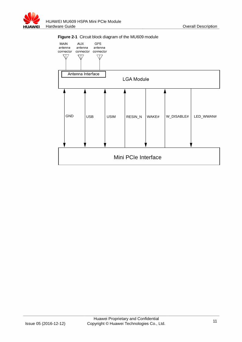
2.3 Circuit Block Diagram Figure 2-1 shows the circuit block diagram of the MU609 Mini PCIe Adapter. The
major functional unit of the Mini PCIe Adapter contains the following parts:
LGA Module
Control signals
Antenna Connectors
HUAWEI MU609 HSPA Mini PCIe Module
Hardware Guide Overall Description
Issue 05 (2016-12-12)
Huawei Proprietary and Confidential
Copyright © Huawei Technologies Co., Ltd. 11
Figure 2-1 Circuit block diagram of the MU609 module
RESIN_N WAKE# W_DISABLE#GND LED_WWAN#USB USIM
Mini PCIe Interface
HUAWEI MU609 HSPA Mini PCIe Module
Hardware Guide Description of the Application Interfaces
Issue 05 (2016-12-12)
Huawei Proprietary and Confidential
Copyright © Huawei Technologies Co., Ltd. 12
3 Description of the Application Interfaces
3.1 About This Chapter This chapter mainly describes the external application interfaces of the MU609 module, including:
Mini PCIe Interface
Power Interface
Signal Control Interface
USB Interface
USIM Card Interface
RF Antenna Connector
Reserved Pins
NC Pins
3.2 Mini PCIe Interface The MU609 module uses a Mini PCIe interface as its external interface. For details about the module and dimensions, see "Dimensions and Interfaces".
HUAWEI MU609 HSPA Mini PCIe Module
Hardware Guide Description of the Application Interfaces
Issue 05 (2016-12-12)
Huawei Proprietary and Confidential
Copyright © Huawei Technologies Co., Ltd. 13
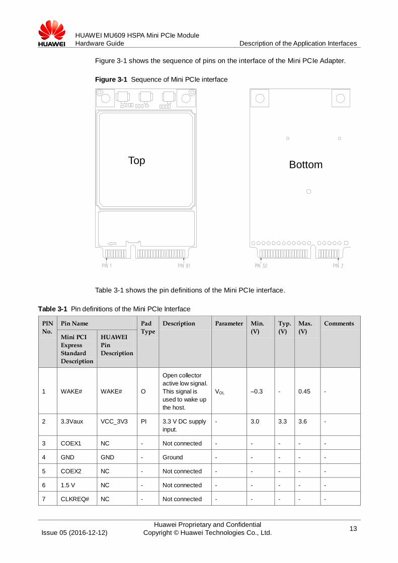
Figure 3-1 shows the sequence of pins on the interface of the Mini PCIe Adapter.
Figure 3-1 Sequence of Mini PCIe interface
Top Bottom
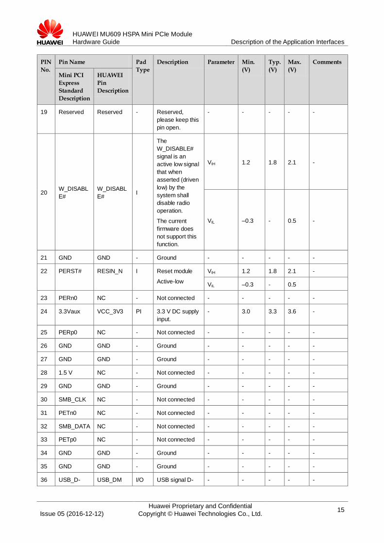
Table 3-1 shows the pin definitions of the Mini PCIe interface.
Table 3-1 Pin definitions of the Mini PCIe Interface
PIN
No.
Pin Name Pad
Type
Description Parameter Min.
(V)
Typ.
(V)
Max.
(V)
Comments
Mini PCI
Express
Standard
Description
HUAWEI
Pin
Description
1 WAKE# WAKE# O
Open collector
active low signal.
This signal is
used to wake up
the host.
VOL –0.3 - 0.45 -
2 3.3Vaux VCC_3V3 PI 3.3 V DC supply
input.
- 3.0 3.3 3.6 -
3 COEX1 NC - Not connected - - - - -
4 GND GND - Ground - - - - -
5 COEX2 NC - Not connected - - - - -
6 1.5 V NC - Not connected - - - - -
7 CLKREQ# NC - Not connected - - - - -
HUAWEI MU609 HSPA Mini PCIe Module
Hardware Guide Description of the Application Interfaces
Issue 05 (2016-12-12)
Huawei Proprietary and Confidential
Copyright © Huawei Technologies Co., Ltd. 14
PIN
No.
Pin Name Pad
Type
Description Parameter Min.
(V)
Typ.
(V)
Max.
(V)
Comments
Mini PCI
Express
Standard
Description
HUAWEI
Pin
Description
8 UIM_PWR USIM_PWR PO
Power source for
the external
USIM card
- 1.75 1.8 1.98 USIM_PWR
=1.8 V
- 2.75 2.85 3.3 USIM_PWR
=2.85 V
9 GND GND - Ground - - - - -
10 UIM_DATA USIM_DAT
A I/O
External USIM
data signal
VIH 0.7 x
USIM_
PWR
- 3.3
USIM_PWR
=1.8 V or
2.85 V
VIL 0 - 0.2 x
USIM_
PWR
VOH 0.7 x
USIM_
PWR
- 3.3
VOL 0 - 0.2 x
USIM_
PWR
11 REFCLK- NC - Not connected - - - - -
12 UIM_CLK USIM_CLK O External USIM
clock signal
VOH 0.7 x
USIM_
PWR
- 3.3 USIM_PWR
=1.8 V or
2.85 V
VOL 0 - 0.2 x
USIM_
PWR
13 REFCLK+ NC - Not connected - - - - -
14 UIM_RESE
T
USIM_RES
ET O
External USIM
reset signal
VOH 0.7 x
USIM_
PWR
- 3.3 USIM_PWR
=1.8 V or
2.85 V
VOL 0 - 0.2 x
USIM_
PWR
15 GND GND - Ground - - - - -
16 UIM_Vpp NC - Not connected - - - - -
17 Reserved Reserved - Reserved,
please keep this
pin open.
- - - - -
18 GND GND - Ground - - - - -
HUAWEI MU609 HSPA Mini PCIe Module
Hardware Guide Description of the Application Interfaces
Issue 05 (2016-12-12)
Huawei Proprietary and Confidential
Copyright © Huawei Technologies Co., Ltd. 15
PIN
No.
Pin Name Pad
Type
Description Parameter Min.
(V)
Typ.
(V)
Max.
(V)
Comments
Mini PCI
Express
Standard
Description
HUAWEI
Pin
Description
19 Reserved Reserved - Reserved,
please keep this
pin open.
- - - - -
20 W_DISABL
E#
W_DISABL
E# I
The
W_DISABLE#
signal is an
active low signal
that when
asserted (driven
low) by the
system shall
disable radio
operation.
The current
firmware does
not support this
function.
VIH 1.2 1.8 2.1 -
VIL –0.3 - 0.5 -
21 GND GND - Ground - - - - -
22 PERST# RESIN_N I Reset module
Active-low
VIH 1.2 1.8 2.1 -
VIL –0.3 - 0.5
23 PERn0 NC - Not connected - - - - -
24 3.3Vaux VCC_3V3 PI 3.3 V DC supply
input.
- 3.0 3.3 3.6 -
25 PERp0 NC - Not connected - - - - -
26 GND GND - Ground - - - - -
27 GND GND - Ground - - - - -
28 1.5 V NC - Not connected - - - - -
29 GND GND - Ground - - - - -
30 SMB_CLK NC - Not connected - - - - -
31 PETn0 NC - Not connected - - - - -
32 SMB_DATA NC - Not connected - - - - -
33 PETp0 NC - Not connected - - - - -
34 GND GND - Ground - - - - -
35 GND GND - Ground - - - - -
36 USB_D- USB_DM I/O USB signal D- - - - - -
HUAWEI MU609 HSPA Mini PCIe Module
Hardware Guide Description of the Application Interfaces
Issue 05 (2016-12-12)
Huawei Proprietary and Confidential
Copyright © Huawei Technologies Co., Ltd. 16
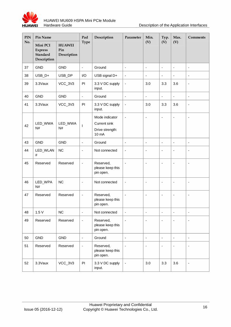
PIN
No.
Pin Name Pad
Type
Description Parameter Min.
(V)
Typ.
(V)
Max.
(V)
Comments
Mini PCI
Express
Standard
Description
HUAWEI
Pin
Description
37 GND GND - Ground - - - - -
38 USB_D+ USB_DP I/O USB signal D+ - - - - -
39 3.3Vaux VCC_3V3 PI 3.3 V DC supply
input.
- 3.0 3.3 3.6 -
40 GND GND - Ground - - - - -
41 3.3Vaux VCC_3V3 PI 3.3 V DC supply
input.
- 3.0 3.3 3.6 -
42 LED_WWA
N#
LED_WWA
N# I
Mode indicator
Current sink
Drive strength:
10 mA
- - - - -
43 GND GND - Ground - - - - -
44 LED_WLAN
#
NC - Not connected - - - - -
45 Reserved Reserved - Reserved,
please keep this
pin open.
- - - - -
46 LED_WPA
N#
NC - Not connected - - - - -
47 Reserved Reserved - Reserved,
please keep this
pin open.
- - - - -
48 1.5 V NC - Not connected - - - - -
49 Reserved Reserved - Reserved,
please keep this
pin open.
- - - - -
50 GND GND - Ground - - - - -
51 Reserved Reserved - Reserved,
please keep this
pin open.
- - - - -
52 3.3Vaux VCC_3V3 PI 3.3 V DC supply
input.
- 3.0 3.3 3.6 -
HUAWEI MU609 HSPA Mini PCIe Module
Hardware Guide Description of the Application Interfaces
Issue 05 (2016-12-12)
Huawei Proprietary and Confidential
Copyright © Huawei Technologies Co., Ltd. 17
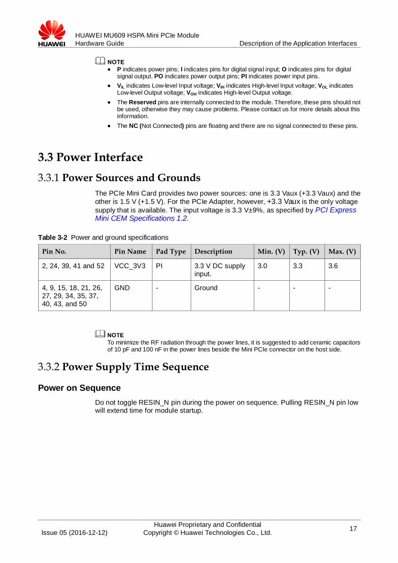
P indicates power pins; I indicates pins for digital signal input; O indicates pins for digital
signal output. PO indicates power output pins; PI indicates power input pins.
VIL indicates Low-level Input voltage; VIH indicates High-level Input voltage; VOL indicates Low-level Output voltage; VOH indicates High-level Output voltage.
The Reserved pins are internally connected to the module. Therefore, these pins should not be used, otherwise they may cause problems. Please contact us for more details about this information.
The NC (Not Connected) pins are floating and there are no signal connected to these pins.
3.3 Power Interface
3.3.1 Power Sources and Grounds
The PCIe Mini Card provides two power sources: one is 3.3 Vaux (+3.3 Vaux) and the
other is 1.5 V (+1.5 V). For the PCIe Adapter, however, +3.3 Vaux is the only voltage
supply that is available. The input voltage is 3.3 V±9%, as specified by PCI Express Mini CEM Specifications 1.2.
Table 3-2 Power and ground specifications
Pin No. Pin Name Pad Type Description Min. (V) Typ. (V) Max. (V)
2, 24, 39, 41 and 52 VCC_3V3 PI 3.3 V DC supply input.
3.0 3.3 3.6
4, 9, 15, 18, 21, 26, 27, 29, 34, 35, 37, 40, 43, and 50
GND - Ground - - -
To minimize the RF radiation through the power lines, it is suggested to add ceramic capacitors of 10 pF and 100 nF in the power lines beside the Mini PCIe connector on the host side.
3.3.2 Power Supply Time Sequence
Power on Sequence
Do not toggle RESIN_N pin during the power on sequence. Pulling RESIN_N pin low will extend time for module startup.
HUAWEI MU609 HSPA Mini PCIe Module
Hardware Guide Description of the Application Interfaces
Issue 05 (2016-12-12)
Huawei Proprietary and Confidential
Copyright © Huawei Technologies Co., Ltd. 18
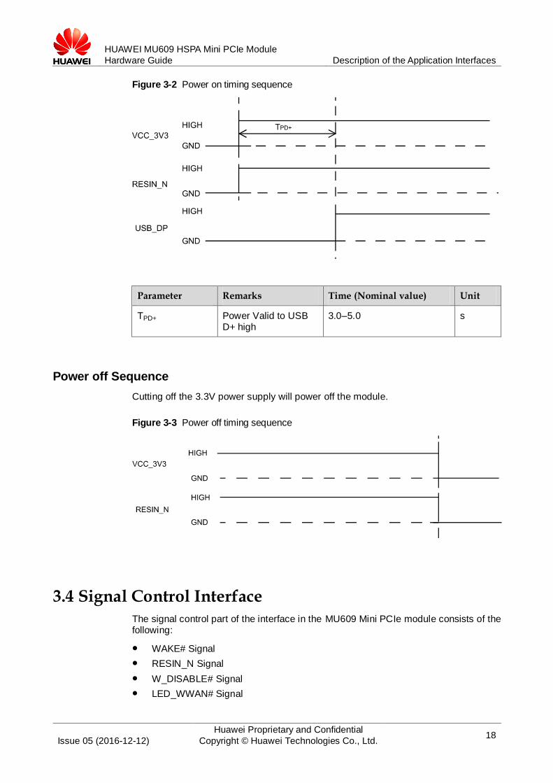
Figure 3-2 Power on timing sequence
Parameter Remarks Time (Nominal value) Unit
TPD+ Power Valid to USB D+ high
3.0–5.0 s
Power off Sequence
Cutting off the 3.3V power supply will power off the module.
Figure 3-3 Power off timing sequence
3.4 Signal Control Interface The signal control part of the interface in the MU609 Mini PCIe module consists of the following:
WAKE# Signal
RESIN_N Signal
W_DISABLE# Signal
LED_WWAN# Signal
HUAWEI MU609 HSPA Mini PCIe Module
Hardware Guide Description of the Application Interfaces
Issue 05 (2016-12-12)
Huawei Proprietary and Confidential
Copyright © Huawei Technologies Co., Ltd. 19
Table 3-3 lists the pins on the signal control interface.
Table 3-3 Definitions of the pins on the signal control interface
Pin No.
Pin Name Pad Type
Description Parameter Min. (V)
Typ. (V)
Max. (V)
1 WAKE# O Open collector active low signal. This signal is used to wake up the host.
VOL –0.3 - 0.45
22 RESIN_N I Reset module
Active-low
VIH 1.2 1.8 2.1
VIL –0.3 - 0.5
20 W_DISABLE# I
The W_DISABLE# signal is an active low signal that when asserted (driven low) by the system shall disable radio operation.
The current firmware does not support this function.
VIH 1.2 1.8 2.1
VIL –0.3 - 0.5
42 LED_WWAN# I
Mode indicator
Current sink
Drive strength: 10 mA
- - - -
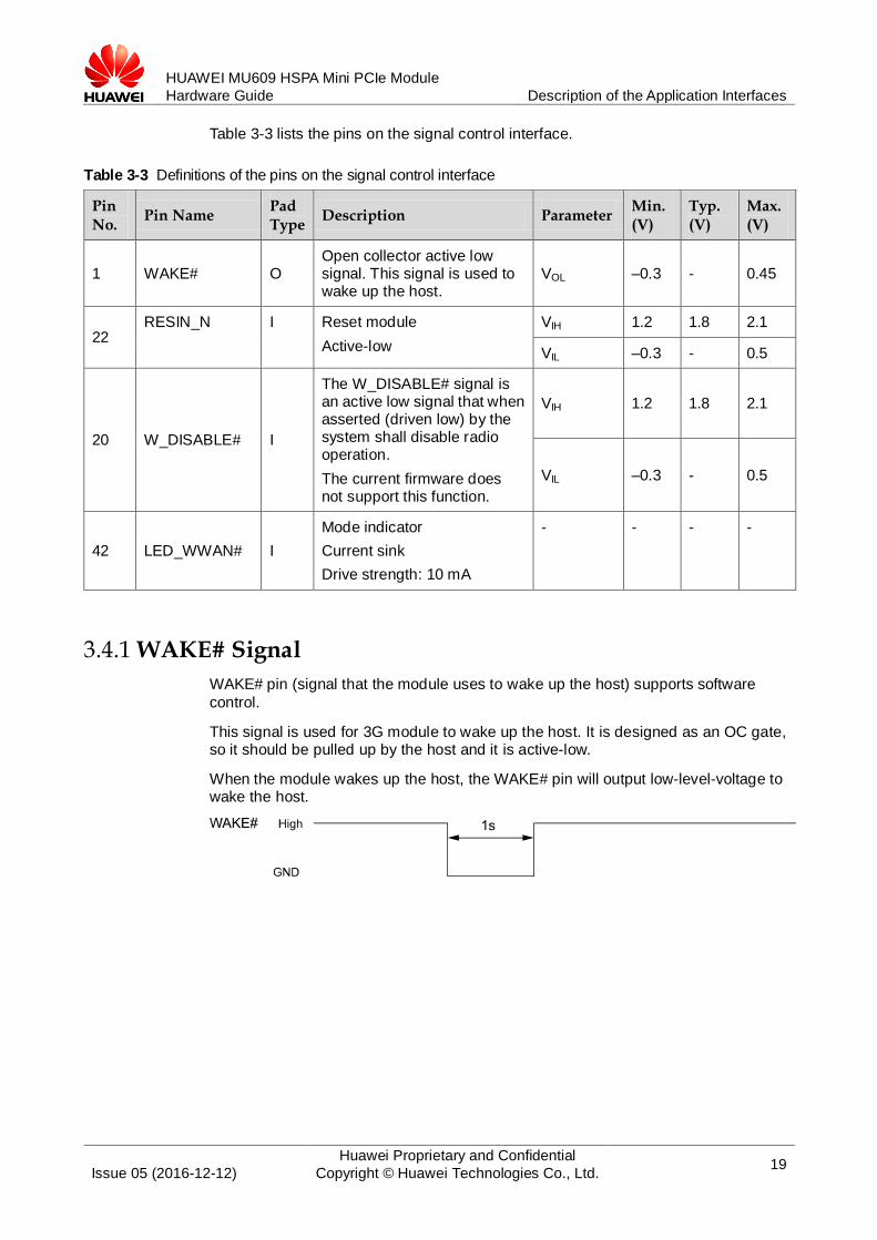
3.4.1 WAKE# Signal
WAKE# pin (signal that the module uses to wake up the host) supports software
control.
This signal is used for 3G module to wake up the host. It is designed as an OC gate, so it should be pulled up by the host and it is active-low.
When the module wakes up the host, the WAKE# pin will output low-level-voltage to wake the host.
HUAWEI MU609 HSPA Mini PCIe Module
Hardware Guide Description of the Application Interfaces
Issue 05 (2016-12-12)
Huawei Proprietary and Confidential
Copyright © Huawei Technologies Co., Ltd. 20
Figure 3-4 Connections of the WAKE# pin
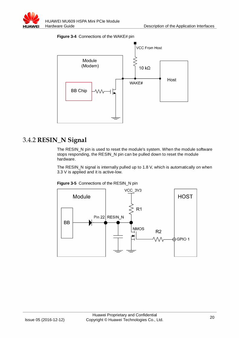
3.4.2 RESIN_N Signal
The RESIN_N pin is used to reset the module's system. When the module software
stops responding, the RESIN_N pin can be pulled down to reset the module hardware.
The RESIN_N signal is internally pulled up to 1.8 V, which is automatically on when 3.3 V is applied and it is active-low.
Figure 3-5 Connections of the RESIN_N pin
HUAWEI MU609 HSPA Mini PCIe Module
Hardware Guide Description of the Application Interfaces
Issue 05 (2016-12-12)
Huawei Proprietary and Confidential
Copyright © Huawei Technologies Co., Ltd. 21
As the RESIN_N signal is relatively sensitive, it is recommended that you install a 10 nF–0.1 µF capacitor near the RESIN_N pin of the interface for filtering. In addition, when you design a circuit on the PCB of the interface board, it is
recommended that the circuit length should not exceed 20 mm and that the circuit should be kept at a distance of 2.54 mm (100 mil) at least from the PCB edge. Furthermore, you need to wrap the area adjacent to the signal wire with a ground wire. Otherwise, the module may be reset due to interference.
The maximum Forward Voltage Drop of the diode used in the module is 0.6 V. So
when the host wants to reset the module, the low-level-voltage in the RESIN_N pin should below 50 mV.
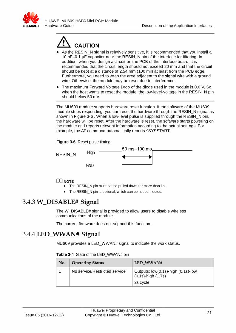
The MU609 module supports hardware reset function. If the software of the MU609 module stops responding, you can reset the hardware through the RESIN_N signal as shown in Figure 3-6 . When a low-level pulse is supplied through the RESIN_N pin, the hardware will be reset. After the hardware is reset, the software starts powering on the module and reports relevant information according to the actual settings. For
example, the AT command automatically reports ^SYSSTART.
Figure 3-6 Reset pulse timing
The RESIN_N pin must not be pulled down for more than 1s.
The RESIN_N pin is optional, which can be not connected.
3.4.3 W_DISABLE# Signal
The W_DISABLE# signal is provided to allow users to disable wireless communications of the module.
The current firmware does not support this function.
3.4.4 LED_WWAN# Signal
MU609 provides a LED_WWAN# signal to indicate the work status.
Table 3-4 State of the LED_WWAN# pin
No. Operating Status LED_WWAN#
1 No service/Restricted service Outputs: low(0.1s)-high (0.1s)-low (0.1s)-high (1.7s)
2s cycle
HUAWEI MU609 HSPA Mini PCIe Module
Hardware Guide Description of the Application Interfaces
Issue 05 (2016-12-12)
Huawei Proprietary and Confidential
Copyright © Huawei Technologies Co., Ltd. 22
No. Operating Status LED_WWAN#
2 Register to the network Outputs: low (0.1s)-high (1.9s)
2s cycle
3 Dial-up successfully Outputs: low
External Circuits
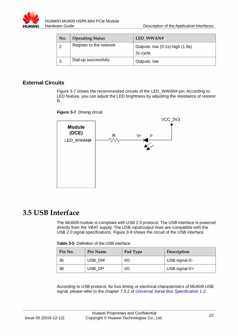
Figure 3-7 shows the recommended circuits of the LED_WWAN# pin. According to
LED feature, you can adjust the LED brightness by adjusting the resistance of resistor R.
Figure 3-7 Driving circuit
3.5 USB Interface
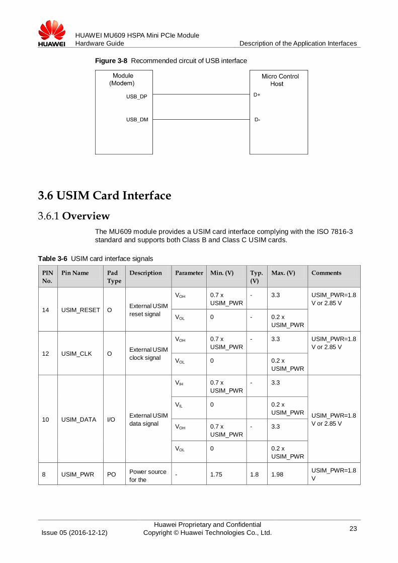
The MU609 module is compliant with USB 2.0 protocol. The USB interface is powered directly from the VBAT supply. The USB input/output lines are compatible with the USB 2.0 signal specifications. Figure 3-8 shows the circuit of the USB interface.
Table 3-5 Definition of the USB interface
Pin No. Pin Name Pad Type Description
36 USB_DM I/O USB signal D-
38 USB_DP I/O USB signal D+
According to USB protocol, for bus timing or electrical characteristics of MU609 USB signal, please refer to the chapter 7.3.2 of Universal Serial Bus Specification 1.2.
HUAWEI MU609 HSPA Mini PCIe Module
Hardware Guide Description of the Application Interfaces
Issue 05 (2016-12-12)
Huawei Proprietary and Confidential
Copyright © Huawei Technologies Co., Ltd. 23
Figure 3-8 Recommended circuit of USB interface
3.6 USIM Card Interface
3.6.1 Overview
The MU609 module provides a USIM card interface complying with the ISO 7816-3
standard and supports both Class B and Class C USIM cards.
Table 3-6 USIM card interface signals
PIN
No.
Pin Name Pad
Type
Description Parameter Min. (V) Typ.
(V)
Max. (V) Comments
14 USIM_RESET O External USIM
reset signal
VOH 0.7 x
USIM_PWR
- 3.3 USIM_PWR=1.8
V or 2.85 V
VOL 0 - 0.2 x
USIM_PWR
12 USIM_CLK O External USIM
clock signal
VOH 0.7 x
USIM_PWR
- 3.3 USIM_PWR=1.8
V or 2.85 V
VOL 0 0.2 x
USIM_PWR
10 USIM_DATA I/O External USIM
data signal
VIH 0.7 x
USIM_PWR
- 3.3
USIM_PWR=1.8
V or 2.85 V
VIL 0 0.2 x
USIM_PWR
VOH 0.7 x
USIM_PWR
- 3.3
VOL 0 0.2 x
USIM_PWR
8 USIM_PWR PO Power source
for the - 1.75 1.8 1.98
USIM_PWR=1.8
V
HUAWEI MU609 HSPA Mini PCIe Module
Hardware Guide Description of the Application Interfaces
Issue 05 (2016-12-12)
Huawei Proprietary and Confidential
Copyright © Huawei Technologies Co., Ltd. 24
PIN
No.
Pin Name Pad
Type
Description Parameter Min. (V) Typ.
(V)
Max. (V) Comments
external USIM
card - 2.75 2.85 3.3 USIM_PWR=2.8
5 V
3.6.2 Circuit Recommended for the USIM Card Interface
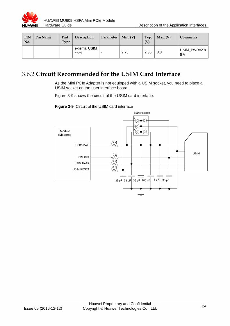
As the Mini PCIe Adapter is not equipped with a USIM socket, you need to place a
USIM socket on the user interface board.
Figure 3-9 shows the circuit of the USIM card interface.
Figure 3-9 Circuit of the USIM card interface
HUAWEI MU609 HSPA Mini PCIe Module
Hardware Guide Description of the Application Interfaces
Issue 05 (2016-12-12)
Huawei Proprietary and Confidential
Copyright © Huawei Technologies Co., Ltd. 25
To meet the requirements of 3GPP TS 51.010-1 protocols and electromagnetic compatibility (EMC) authentication, the USIM socket should be placed near the PCIe interface (it is recommended that the PCB circuit connects the PCIe interface
and the USIM socket does not exceed 100 mm), because a long circuit may lead to wave distortion, thus affecting signal quality.
It is recommended that you wrap the area adjacent to the USIM_CLK and USIM_DATA signal wires with ground. The Ground pin of the USIM socket and the Ground pin of the USIM card must be well connected to the power Ground pin supplying power to the PCIe Adapter.
A 100 nF capacitor and1 μF capacitor are placed between the USIM_PWR and GND pins in a parallel manner (If USIM_PWR circuit is too long, that the larger capacitance such as 4.7 μF can be employed if necessary). Three 33 pF capacitors are placed between the USIM_DATA and Ground pins, the USIM_RESET and Ground pins, and the USIM_CLK and Ground pins in parallel to
filter interference from RF signals.
It is recommended to take electrostatic discharge (ESD) protection measures near the USIM card socket. The TVS diode with Vrwm of 5 V and junction capacitance less than 10 pF must be placed as close as possible to the USIM socket, and the Ground pin of the ESD protection component is well connected to the power
Ground pin that supplies power to the PCIe Adapter.
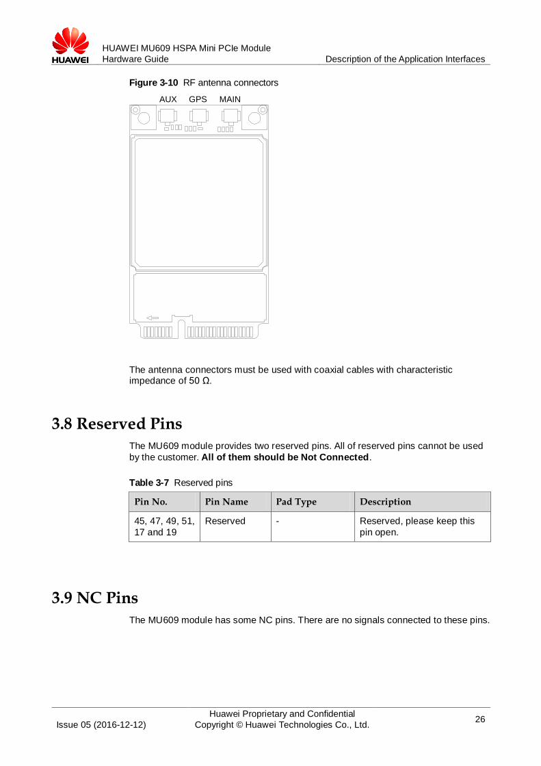
3.7 RF Antenna Connector
The MU609 module provides three antenna connectors (MAIN, GPS and AUX) for connecting the external antennas.
HUAWEI MU609 HSPA Mini PCIe Module
Hardware Guide Description of the Application Interfaces
Issue 05 (2016-12-12)
Huawei Proprietary and Confidential
Copyright © Huawei Technologies Co., Ltd. 26
Figure 3-10 RF antenna connectors
AUX GPS MAIN
The antenna connectors must be used with coaxial cables with characteristic impedance of 50 Ω.
3.8 Reserved Pins The MU609 module provides two reserved pins. All of reserved pins cannot be used
by the customer. All of them should be Not Connected.
Table 3-7 Reserved pins
Pin No. Pin Name Pad Type Description
45, 47, 49, 51,
17 and 19
Reserved - Reserved, please keep this
pin open.
3.9 NC Pins The MU609 module has some NC pins. There are no signals connected to these pins.
HUAWEI MU609 HSPA Mini PCIe Module
Hardware Guide Description of the Application Interfaces
Issue 05 (2016-12-12)
Huawei Proprietary and Confidential
Copyright © Huawei Technologies Co., Ltd. 27
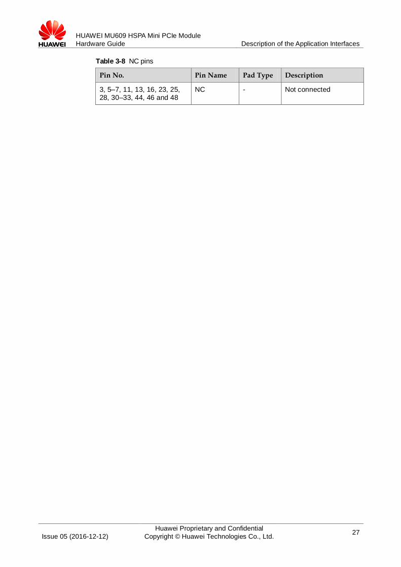
Table 3-8 NC pins
Pin No. Pin Name Pad Type Description
3, 5–7, 11, 13, 16, 23, 25, 28, 30–33, 44, 46 and 48
NC - Not connected
HUAWEI MU609 HSPA Mini PCIe Module
Hardware Guide RF Specifications
Issue 05 (2016-12-12)
Huawei Proprietary and Confidential
Copyright © Huawei Technologies Co., Ltd. 28
4 RF Specifications
4.1 About This Chapter This chapter describes the RF specifications of the MU609 module, including:
Operating Frequencies
Conducted RF Measurement
Conducted Rx Sensitivity and Tx Power
Antenna Design Requirements
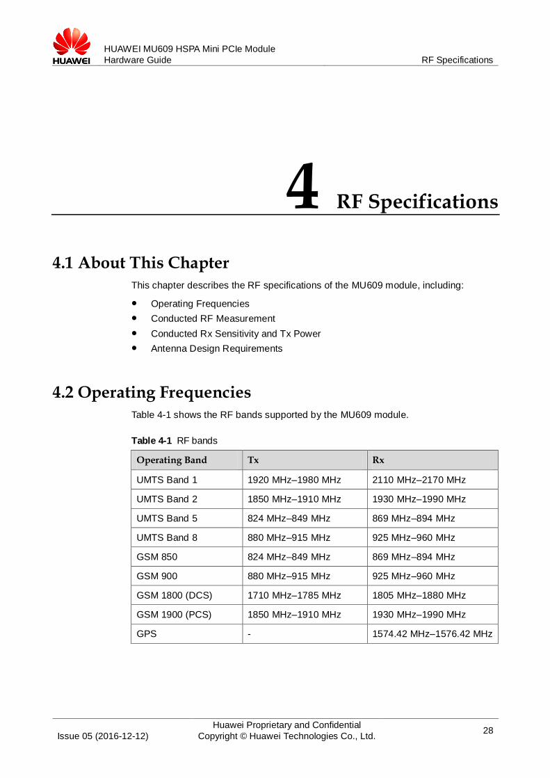
4.2 Operating Frequencies Table 4-1 shows the RF bands supported by the MU609 module.
Table 4-1 RF bands
Operating Band Tx Rx
UMTS Band 1 1920 MHz–1980 MHz 2110 MHz–2170 MHz
UMTS Band 2 1850 MHz–1910 MHz 1930 MHz–1990 MHz
UMTS Band 5 824 MHz–849 MHz 869 MHz–894 MHz
UMTS Band 8 880 MHz–915 MHz 925 MHz–960 MHz
GSM 850 824 MHz–849 MHz 869 MHz–894 MHz
GSM 900 880 MHz–915 MHz 925 MHz–960 MHz
GSM 1800 (DCS) 1710 MHz–1785 MHz 1805 MHz–1880 MHz
GSM 1900 (PCS) 1850 MHz–1910 MHz 1930 MHz–1990 MHz
GPS - 1574.42 MHz–1576.42 MHz
HUAWEI MU609 HSPA Mini PCIe Module
Hardware Guide RF Specifications
Issue 05 (2016-12-12)
Huawei Proprietary and Confidential
Copyright © Huawei Technologies Co., Ltd. 29
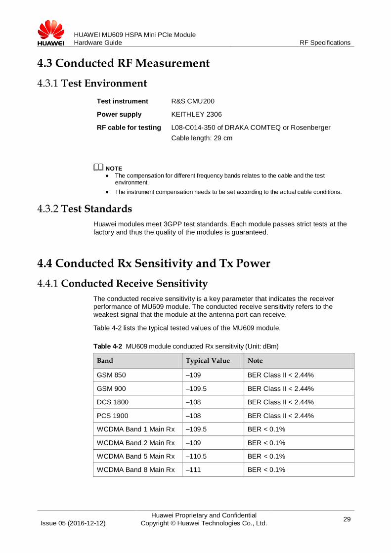
4.3 Conducted RF Measurement
4.3.1 Test Environment
Test instrument R&S CMU200
Power supply KEITHLEY 2306
RF cable for testing L08-C014-350 of DRAKA COMTEQ or Rosenberger
Cable length: 29 cm
The compensation for different frequency bands relates to the cable and the test
environment.
The instrument compensation needs to be set according to the actual cable conditions.
4.3.2 Test Standards
Huawei modules meet 3GPP test standards. Each module passes strict tests at the
factory and thus the quality of the modules is guaranteed.
4.4 Conducted Rx Sensitivity and Tx Power
4.4.1 Conducted Receive Sensitivity
The conducted receive sensitivity is a key parameter that indicates the receiver performance of MU609 module. The conducted receive sensitivity refers to the weakest signal that the module at the antenna port can receive.
Table 4-2 lists the typical tested values of the MU609 module.
Table 4-2 MU609 module conducted Rx sensitivity (Unit: dBm)
Band Typical Value Note
GSM 850 –109 BER Class II < 2.44%
GSM 900 –109.5 BER Class II < 2.44%
DCS 1800 –108 BER Class II < 2.44%
PCS 1900 –108 BER Class II < 2.44%
WCDMA Band 1 Main Rx –109.5 BER < 0.1%
WCDMA Band 2 Main Rx –109 BER < 0.1%
WCDMA Band 5 Main Rx –110.5 BER < 0.1%
WCDMA Band 8 Main Rx –111 BER < 0.1%
HUAWEI MU609 HSPA Mini PCIe Module
Hardware Guide RF Specifications
Issue 05 (2016-12-12)
Huawei Proprietary and Confidential
Copyright © Huawei Technologies Co., Ltd. 30
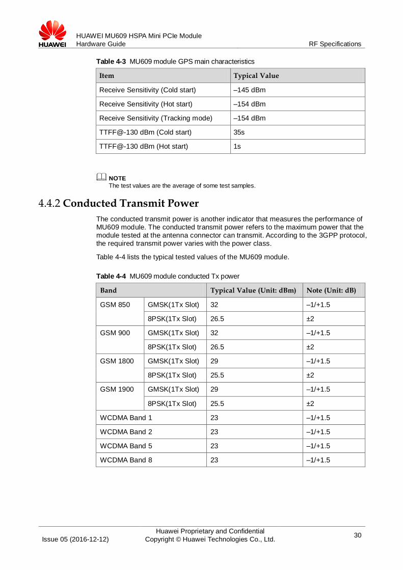
Table 4-3 MU609 module GPS main characteristics
Item Typical Value
Receive Sensitivity (Cold start) –145 dBm
Receive Sensitivity (Hot start) –154 dBm
Receive Sensitivity (Tracking mode) –154 dBm
TTFF@-130 dBm (Cold start) 35s
TTFF@-130 dBm (Hot start) 1s
The test values are the average of some test samples.
4.4.2 Conducted Transmit Power
The conducted transmit power is another indicator that measures the performance of MU609 module. The conducted transmit power refers to the maximum power that the module tested at the antenna connector can transmit. According to the 3GPP protocol, the required transmit power varies with the power class.
Table 4-4 lists the typical tested values of the MU609 module.
Table 4-4 MU609 module conducted Tx power
Band Typical Value (Unit: dBm) Note (Unit: dB)
GSM 850 GMSK(1Tx Slot) 32 –1/+1.5
8PSK(1Tx Slot) 26.5 ±2
GSM 900 GMSK(1Tx Slot) 32 –1/+1.5
8PSK(1Tx Slot) 26.5 ±2
GSM 1800 GMSK(1Tx Slot) 29 –1/+1.5
8PSK(1Tx Slot) 25.5 ±2
GSM 1900 GMSK(1Tx Slot) 29 –1/+1.5
8PSK(1Tx Slot) 25.5 ±2
WCDMA Band 1 23 –1/+1.5
WCDMA Band 2 23 –1/+1.5
WCDMA Band 5 23 –1/+1.5
WCDMA Band 8 23 –1/+1.5
HUAWEI MU609 HSPA Mini PCIe Module
Hardware Guide RF Specifications
Issue 05 (2016-12-12)
Huawei Proprietary and Confidential
Copyright © Huawei Technologies Co., Ltd. 31
4.5 Antenna Design Requirements
4.5.1 Antenna Design Indicators
Antenna Efficiency
Antenna efficiency is the ratio of the input power to the radiated or received power of an antenna. The radiated power of an antenna is always lower than the input power due to the following antenna losses: return loss, material loss, and coupling loss. The efficiency of an antenna relates to its electrical dimensions. To be specific, the
antenna efficiency increases with the electrical dimensions. In addition, the transmission cable from the antenna connector of PCIe Adapter to the antenna is also part of the antenna. The cable loss increases with the cable length and the frequency. It is recommended that the cable loss is as low as possible, for example, U.FL-LP-088 made by HRS.
The following antenna efficiency (free space) is recommended for MU609 module to
ensure high radio performance of the module:
Efficiency of the primary antenna: ≥ 40% (below 960 MHz); ≥ 50% (over 1710 MHz)
Efficiency of the diversity antenna: ≥ half of the efficiency of the primary antenna in receiving band
Efficiency of the GPS antenna: ≥ 50%
In addition, the efficiency should be tested with the transmission cable.
S11 (VSWR)
S11 indicates the degree to which the input impedance of an antenna matches the reference impedance (50 Ω). S11 shows the resonance feature and impedance bandwidth of an antenna. Voltage standing wave ratio (VSWR) is another expression of S11. S11 relates to the antenna efficiency. S11 can be measured with a vector
analyzer.
The following S11 value is recommended for the antenna of MU609 module:
S11 of the primary antenna: ≤ –6 dB
S11 of the diversity antenna: ≤ –6 dB
S11 of the GPS antenna: ≤ –10 dB
In addition, S11 is less important than the efficiency, and S11 has weak correlation to
wireless performance.
Isolation
For a wireless device with multiple antennas, the power of different antennas is coupled with each other. Antenna isolation is used to measure the power coupling. The power radiated by an antenna might be received by an adjacent antenna, which decreases the antenna radiation efficiency and affects the running of other devices. To avoid this problem, evaluate the antenna isolation as sufficiently as possible at the
early stage of antenna design.
Antenna isolation depends on the following factors:
HUAWEI MU609 HSPA Mini PCIe Module
Hardware Guide RF Specifications
Issue 05 (2016-12-12)
Huawei Proprietary and Confidential
Copyright © Huawei Technologies Co., Ltd. 32
Distance between antennas
Antenna type
Antenna direction
The primary antenna must be placed as near as possible to the MU609 module to
minimize the cable length. The diversity antenna needs to be installed
perpendicularly to the primary antenna. The diversity antenna can be placed farther away from the MU609 module. Antenna isolation can be measured with a two-port vector network analyzer.
The following antenna isolation is recommended for the antennas on laptops:
Isolation between the primary and diversity antennas: ≤ –12 dB
Isolation between the primary(diversity) antenna and the GPS antenna: ≤ –15 dB
Isolation between the primary antenna and the Wi-Fi antenna: ≤ –15 dB
Polarization
The polarization of an antenna is the orientation of the electric field vector that rotates
with time in the direction of maximum radiation.
The linear polarization is recommended for the antenna of MU609 module.
Radiation Pattern
The radiation pattern of an antenna reflects the radiation features of the antenna in the remote field region. The radiation pattern of an antenna commonly describes the power or field strength of the radiated electromagnetic waves in various directions from the antenna. The power or field strength varies with the angular coordinates (θ
and φ), but is independent of the radial coordinates.
The radiation pattern of half wave dipole antennas is omnidirectional in the horizontal plane, and the incident waves of base stations are often in the horizontal plane. For this reason, the receiving performance is optimal.
The following radiation patterns are recommended for the antenna of MU609 module.
Primary/Diversity/GPS antenna: omnidirectional
In addition, the diversity antenna's pattern should be complementary with the primary's.
Envelope Correlation Coefficient
The envelope correlation coefficient indicates the correlation between different antennas in a multi-antenna system (primary antenna, diversity antenna, and MIMO antenna). The correlation coefficient shows the similarity of radiation patterns, that is, amplitude and phase, of the antennas. The ideal correlation coefficient of a diversity
antenna system or a MIMO antenna system is 0. A small value of the envelope correlation coefficient between the primary antenna and the diversity antenna indicates a high diversity gain. The envelope correlation coefficient depends on the following factors:
Distance between antennas
Antenna type
HUAWEI MU609 HSPA Mini PCIe Module
Hardware Guide RF Specifications
Issue 05 (2016-12-12)
Huawei Proprietary and Confidential
Copyright © Huawei Technologies Co., Ltd. 33
Antenna direction
The antenna correlation coefficient differs from the antenna isolation. Sufficient antenna isolation does not represent a satisfactory correlation coefficient. For this reason, the two indicators need to be evaluated separately.
For the antennas on laptops, the recommended envelope correlation coefficient
between the primary antenna and the diversity antenna is smaller than 0.5.
Gain and Directivity
The radiation pattern of an antenna represents the field strength of the radiated electromagnetic waves in all directions, but not the power density that the antenna radiates in the specific direction. The directivity of an antenna, however, measures the power density that the antenna radiates.
Gain, as another important parameter of antennas, correlates closely to the directivity.
The gain of an antenna takes both the directivity and the efficiency of the antenna into account. The appropriate antenna gain prolongs the service life of relevant batteries.
The following antenna gain is recommended for MU609 module. Gain of the primary/diversity antenna ≤ 2.5 dBi
The antenna consists of the antenna body and the relevant RF transmission cable. Take the
RF transmission cable into account when measuring any of the preceding antenna indicators.
Huawei cooperates with various famous antenna suppliers who are able to make suggestions on antenna design, for example, Amphenol, Skycross, etc.
4.5.2 Interference
Besides the antenna performance, the interference on the user board also affects the radio performance (especially the TIS) of the module. To guarantee high performance of the module, the interference sources on the user board must be properly controlled.
On the user board, there are various interference sources, such as the LCD, CPU, audio circuits, and power supply. All the interference sources emit interference signals
that affect the normal operation of the module. For example, the module sensitivity can be decreased due to interference signals. Therefore, during the design, you need to consider how to reduce the effects of interference sources on the module. You can take the following measures: Use an LCD with optimized performance; shield the LCD interference signals; shield the signal cable of the board; or design filter circuits.
Huawei is able to make technical suggestions on radio performance improvement of the module.
4.5.3 Antenna Requirements
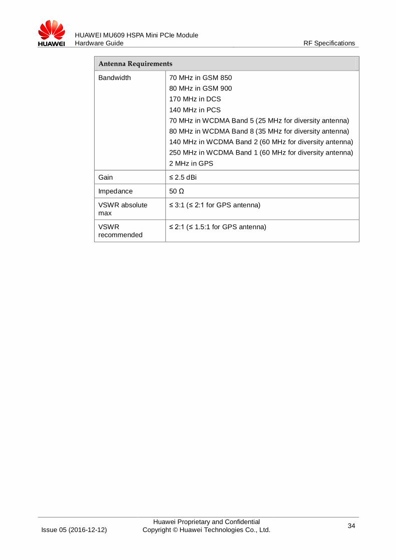
The antenna for MU609 module must fulfill the following requirements:
Antenna Requirements
Frequency range Depending on frequency band(s) provided by the network
operator, the customer must use the most suitable antenna for that/those band(s)
HUAWEI MU609 HSPA Mini PCIe Module
Hardware Guide RF Specifications
Issue 05 (2016-12-12)
Huawei Proprietary and Confidential
Copyright © Huawei Technologies Co., Ltd. 34
Antenna Requirements
Bandwidth 70 MHz in GSM 850
80 MHz in GSM 900
170 MHz in DCS
140 MHz in PCS
70 MHz in WCDMA Band 5 (25 MHz for diversity antenna)
80 MHz in WCDMA Band 8 (35 MHz for diversity antenna)
140 MHz in WCDMA Band 2 (60 MHz for diversity antenna)
250 MHz in WCDMA Band 1 (60 MHz for diversity antenna)
2 MHz in GPS
Gain ≤ 2.5 dBi
Impedance 50 Ω
VSWR absolute max
≤ 3:1 (≤ 2:1 for GPS antenna)
VSWR recommended
≤ 2:1 (≤ 1.5:1 for GPS antenna)
HUAWEI MU609 HSPA Mini PCIe Module
Hardware Guide Electrical and Reliability Features
Issue 05 (2016-12-12)
Huawei Proprietary and Confidential
Copyright © Huawei Technologies Co., Ltd. 35
5 Electrical and Reliability Features
5.1 About This Chapter This chapter describes the electrical and reliability features of the interfaces in the MU609 module, including:
Absolute Ratings
Operating and Storage Temperatures
Power Supply Features
Reliability Features
EMC and ESD Features
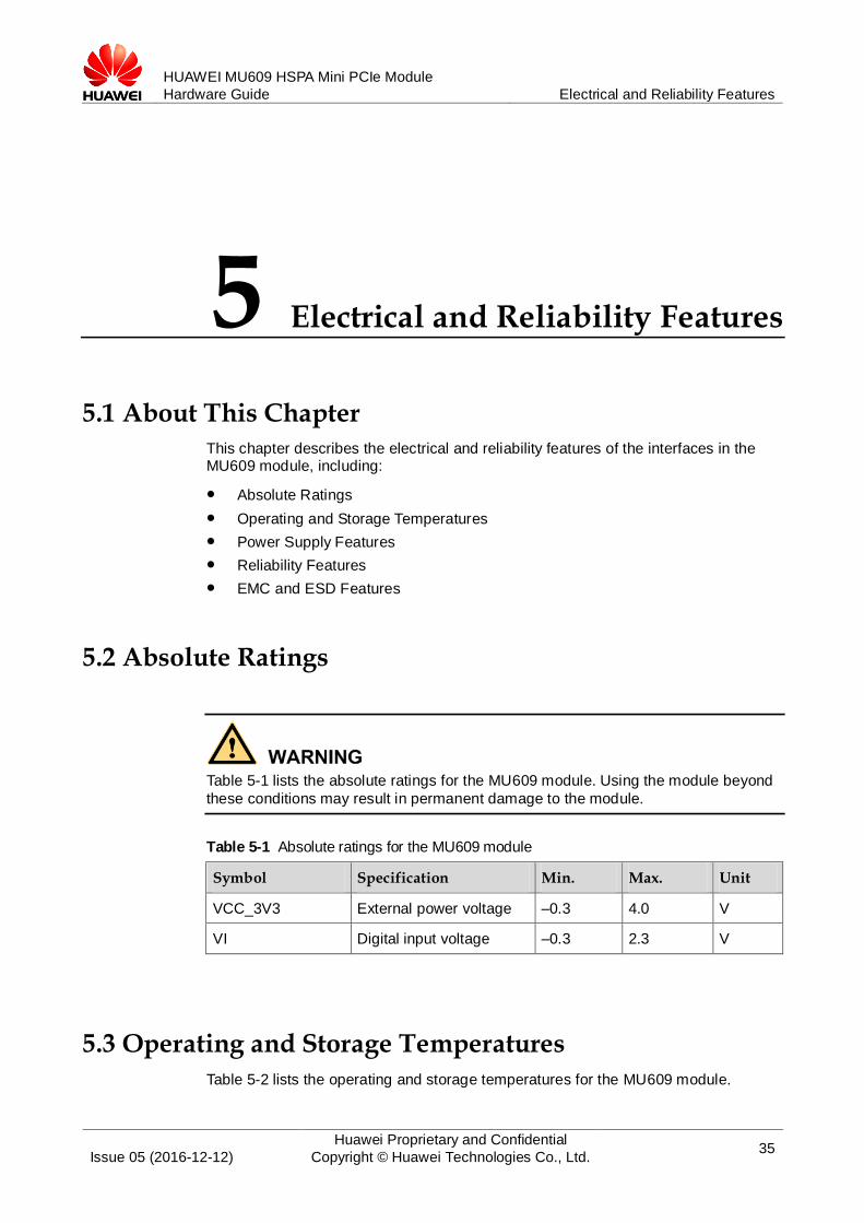
5.2 Absolute Ratings
Table 5-1 lists the absolute ratings for the MU609 module. Using the module beyond
these conditions may result in permanent damage to the module.
Table 5-1 Absolute ratings for the MU609 module
Symbol Specification Min. Max. Unit
VCC_3V3 External power voltage –0.3 4.0 V
VI Digital input voltage –0.3 2.3 V
5.3 Operating and Storage Temperatures
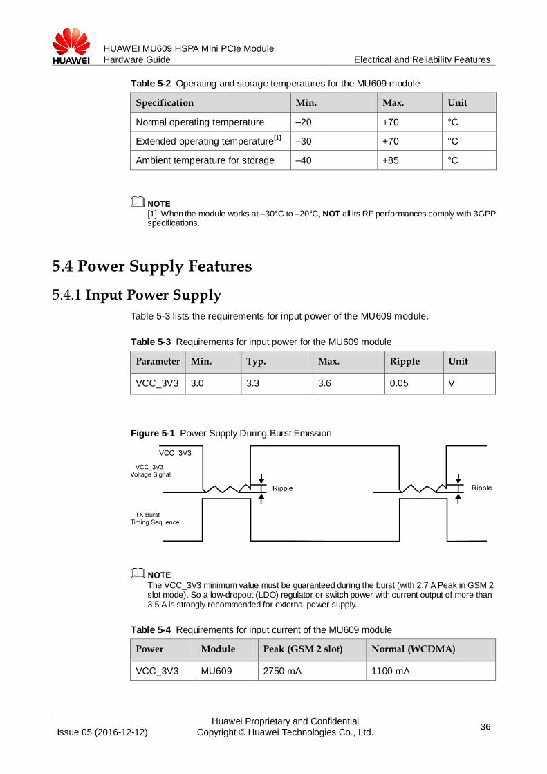
Table 5-2 lists the operating and storage temperatures for the MU609 module.
HUAWEI MU609 HSPA Mini PCIe Module
Hardware Guide Electrical and Reliability Features
Issue 05 (2016-12-12)
Huawei Proprietary and Confidential
Copyright © Huawei Technologies Co., Ltd. 36
Table 5-2 Operating and storage temperatures for the MU609 module
Specification Min. Max. Unit
Normal operating temperature –20 +70 °C
Extended operating temperature[1]
–30 +70 °C
Ambient temperature for storage –40 +85 °C
[1]: When the module works at –30°C to –20°C, NOT all its RF performances comply with 3GPP specifications.
5.4 Power Supply Features
5.4.1 Input Power Supply
Table 5-3 lists the requirements for input power of the MU609 module.
Table 5-3 Requirements for input power for the MU609 module
Parameter Min. Typ. Max. Ripple Unit
VCC_3V3 3.0 3.3 3.6 0.05 V
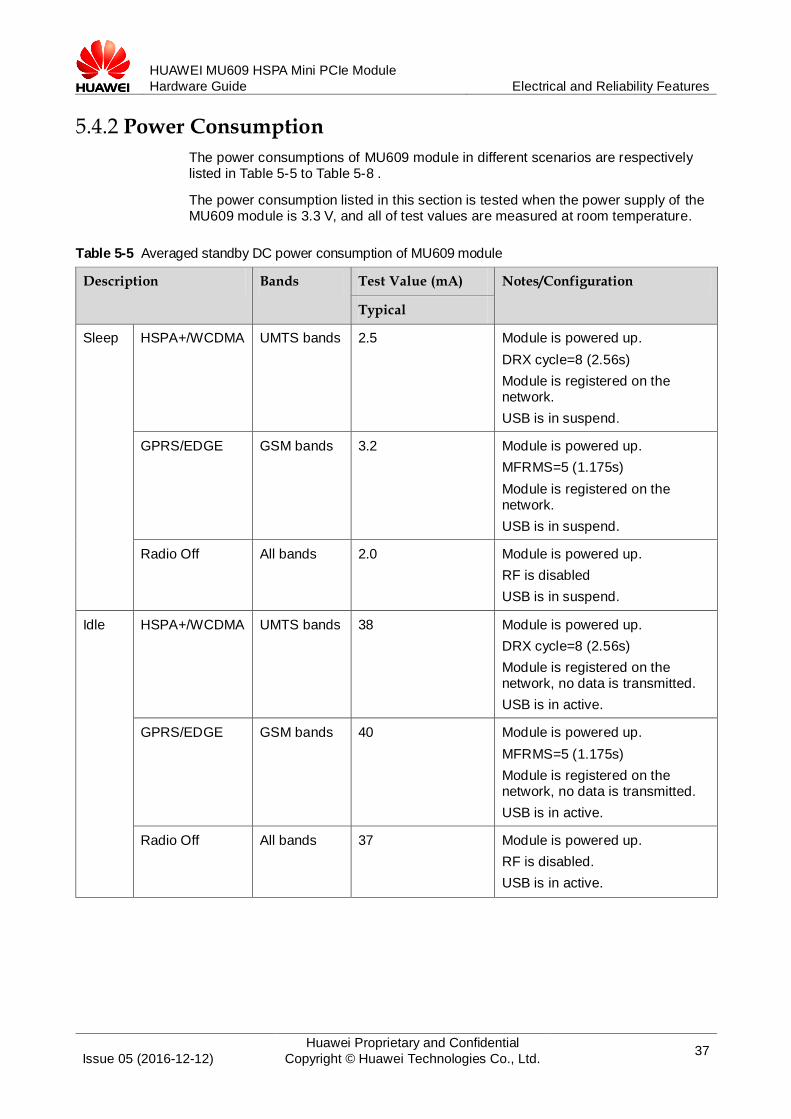
Figure 5-1 Power Supply During Burst Emission
The VCC_3V3 minimum value must be guaranteed during the burst (with 2.7 A Peak in GSM 2 slot mode). So a low-dropout (LDO) regulator or switch power with current output of more than 3.5 A is strongly recommended for external power supply.
Table 5-4 Requirements for input current of the MU609 module
Power Module Peak (GSM 2 slot) Normal (WCDMA)
VCC_3V3 MU609 2750 mA 1100 mA
HUAWEI MU609 HSPA Mini PCIe Module
Hardware Guide Electrical and Reliability Features
Issue 05 (2016-12-12)
Huawei Proprietary and Confidential
Copyright © Huawei Technologies Co., Ltd. 37
5.4.2 Power Consumption
The power consumptions of MU609 module in different scenarios are respectively listed in Table 5-5 to Table 5-8 .
The power consumption listed in this section is tested when the power supply of the MU609 module is 3.3 V, and all of test values are measured at room temperature.
Table 5-5 Averaged standby DC power consumption of MU609 module
Description Bands Test Value (mA) Notes/Configuration
Typical
Sleep HSPA+/WCDMA UMTS bands 2.5 Module is powered up.
DRX cycle=8 (2.56s)
Module is registered on the network.
USB is in suspend.
GPRS/EDGE GSM bands 3.2 Module is powered up.
MFRMS=5 (1.175s)
Module is registered on the network.
USB is in suspend.
Radio Off All bands 2.0 Module is powered up.
RF is disabled
USB is in suspend.
Idle HSPA+/WCDMA UMTS bands 38 Module is powered up.
DRX cycle=8 (2.56s)
Module is registered on the network, no data is transmitted.
USB is in active.
GPRS/EDGE GSM bands 40 Module is powered up.
MFRMS=5 (1.175s)
Module is registered on the network, no data is transmitted.
USB is in active.
Radio Off All bands 37 Module is powered up.
RF is disabled.
USB is in active.
HUAWEI MU609 HSPA Mini PCIe Module
Hardware Guide Electrical and Reliability Features
Issue 05 (2016-12-12)
Huawei Proprietary and Confidential
Copyright © Huawei Technologies Co., Ltd. 38
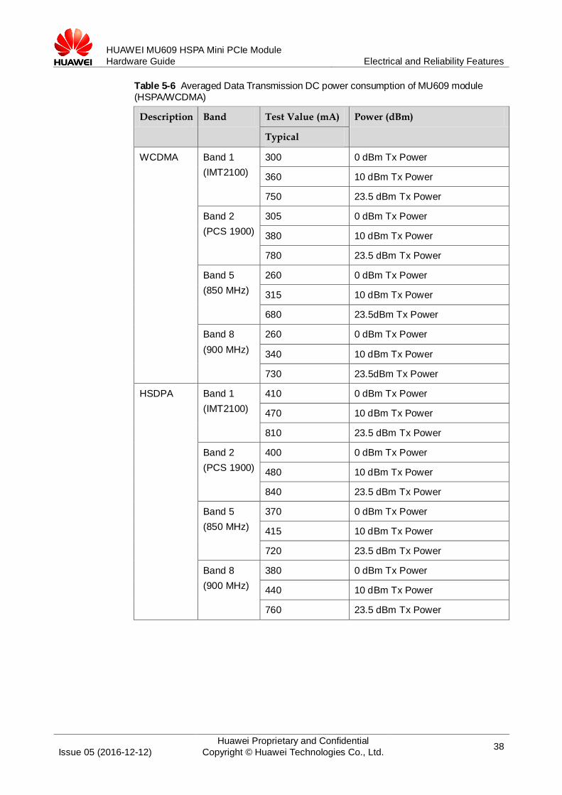
Table 5-6 Averaged Data Transmission DC power consumption of MU609 module (HSPA/WCDMA)
Description Band Test Value (mA) Power (dBm)
Typical
WCDMA Band 1
(IMT2100)
300 0 dBm Tx Power
360 10 dBm Tx Power
750 23.5 dBm Tx Power
Band 2
(PCS 1900)
305 0 dBm Tx Power
380 10 dBm Tx Power
780 23.5 dBm Tx Power
Band 5
(850 MHz)
260 0 dBm Tx Power
315 10 dBm Tx Power
680 23.5dBm Tx Power
Band 8
(900 MHz)
260 0 dBm Tx Power
340 10 dBm Tx Power
730 23.5dBm Tx Power
HSDPA Band 1
(IMT2100)
410 0 dBm Tx Power
470 10 dBm Tx Power
810 23.5 dBm Tx Power
Band 2
(PCS 1900)
400 0 dBm Tx Power
480 10 dBm Tx Power
840 23.5 dBm Tx Power
Band 5
(850 MHz)
370 0 dBm Tx Power
415 10 dBm Tx Power
720 23.5 dBm Tx Power
Band 8
(900 MHz)
380 0 dBm Tx Power
440 10 dBm Tx Power
760 23.5 dBm Tx Power
HUAWEI MU609 HSPA Mini PCIe Module
Hardware Guide Electrical and Reliability Features
Issue 05 (2016-12-12)
Huawei Proprietary and Confidential
Copyright © Huawei Technologies Co., Ltd. 39
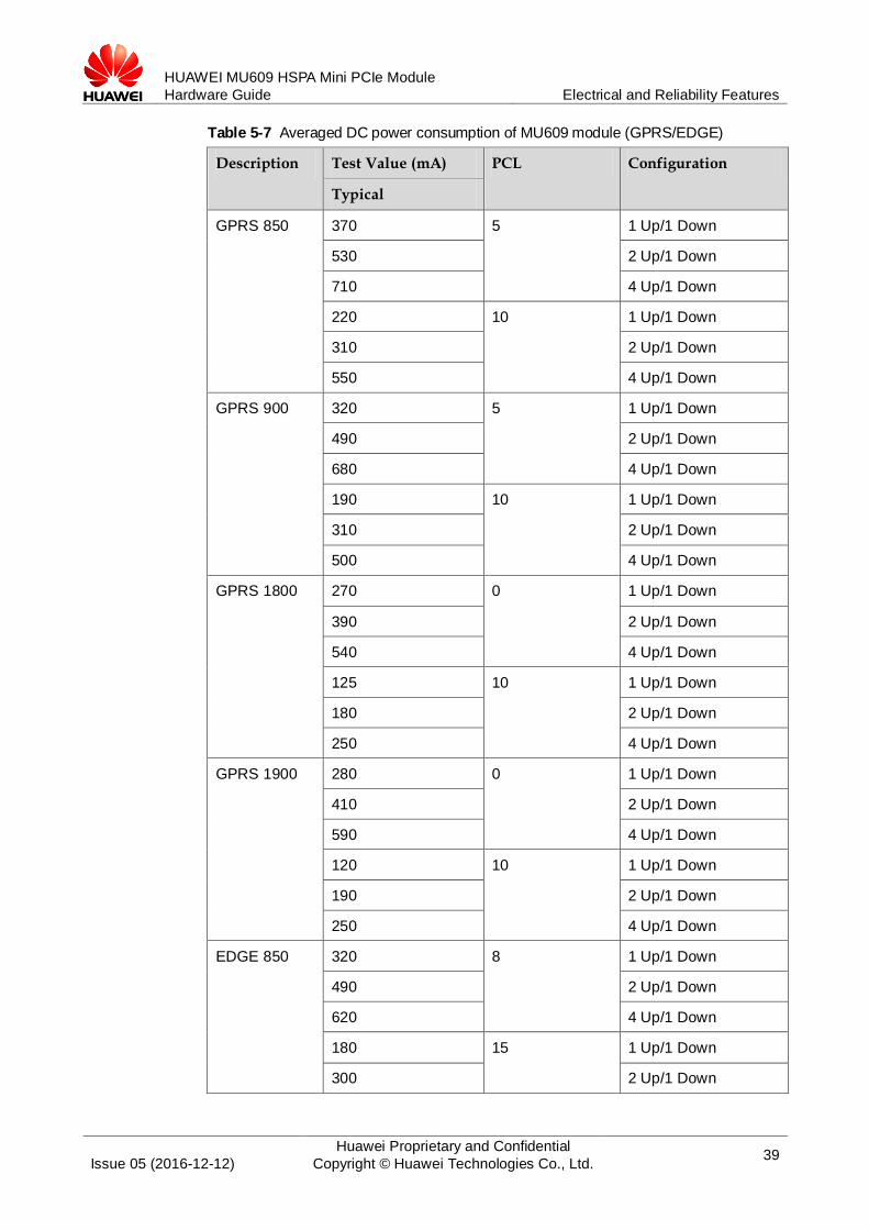
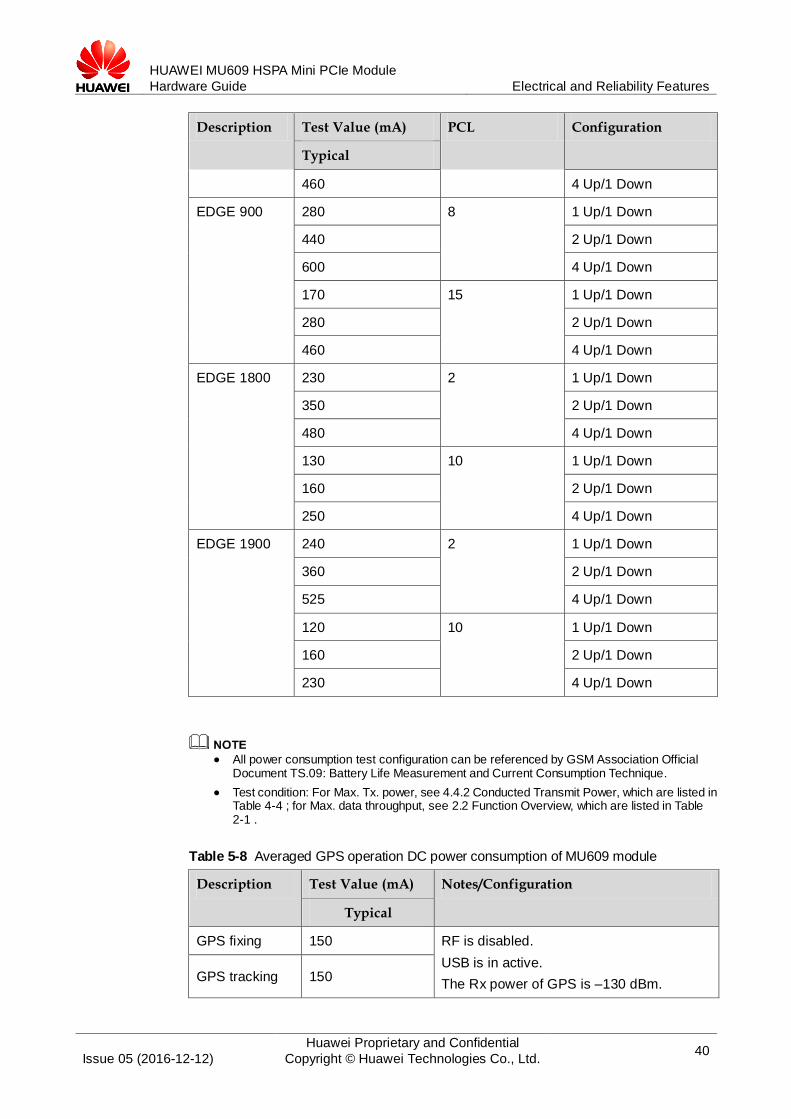
Table 5-7 Averaged DC power consumption of MU609 module (GPRS/EDGE)
Description Test Value (mA) PCL Configuration
Typical
GPRS 850 370 5 1 Up/1 Down
530 2 Up/1 Down
710 4 Up/1 Down
220 10 1 Up/1 Down
310 2 Up/1 Down
550 4 Up/1 Down
GPRS 900 320 5 1 Up/1 Down
490 2 Up/1 Down
680 4 Up/1 Down
190 10 1 Up/1 Down
310 2 Up/1 Down
500 4 Up/1 Down
GPRS 1800 270 0 1 Up/1 Down
390 2 Up/1 Down
540 4 Up/1 Down
125 10 1 Up/1 Down
180 2 Up/1 Down
250 4 Up/1 Down
GPRS 1900 280 0 1 Up/1 Down
410 2 Up/1 Down
590 4 Up/1 Down
120 10 1 Up/1 Down
190 2 Up/1 Down
250 4 Up/1 Down
EDGE 850 320 8 1 Up/1 Down
490 2 Up/1 Down
620 4 Up/1 Down
180 15 1 Up/1 Down
300 2 Up/1 Down
HUAWEI MU609 HSPA Mini PCIe Module
Hardware Guide Electrical and Reliability Features
Issue 05 (2016-12-12)
Huawei Proprietary and Confidential
Copyright © Huawei Technologies Co., Ltd. 40
Description Test Value (mA) PCL Configuration
Typical
460 4 Up/1 Down
EDGE 900 280 8 1 Up/1 Down
440 2 Up/1 Down
600 4 Up/1 Down
170 15 1 Up/1 Down
280 2 Up/1 Down
460 4 Up/1 Down
EDGE 1800 230 2 1 Up/1 Down
350 2 Up/1 Down
480 4 Up/1 Down
130 10 1 Up/1 Down
160 2 Up/1 Down
250 4 Up/1 Down
EDGE 1900 240 2 1 Up/1 Down
360 2 Up/1 Down
525 4 Up/1 Down
120 10 1 Up/1 Down
160 2 Up/1 Down
230 4 Up/1 Down
All power consumption test configuration can be referenced by GSM Association Official
Document TS.09: Battery Life Measurement and Current Consumption Technique.
Test condition: For Max. Tx. power, see 4.4.2 Conducted Transmit Power, which are listed in Table 4-4 ; for Max. data throughput, see 2.2 Function Overview, which are listed in Table 2-1 .
Table 5-8 Averaged GPS operation DC power consumption of MU609 module
Description Test Value (mA) Notes/Configuration
Typical
GPS fixing 150 RF is disabled.
USB is in active.
The Rx power of GPS is –130 dBm. GPS tracking 150
HUAWEI MU609 HSPA Mini PCIe Module
Hardware Guide Electrical and Reliability Features
Issue 05 (2016-12-12)
Huawei Proprietary and Confidential
Copyright © Huawei Technologies Co., Ltd. 41
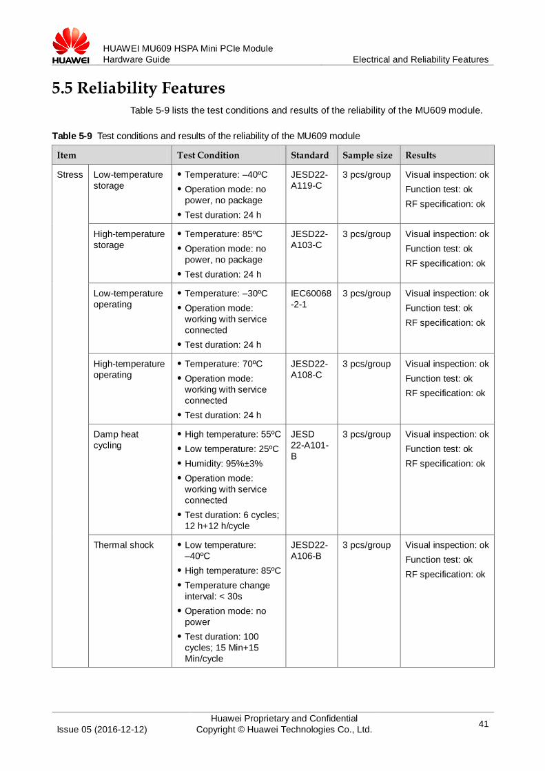
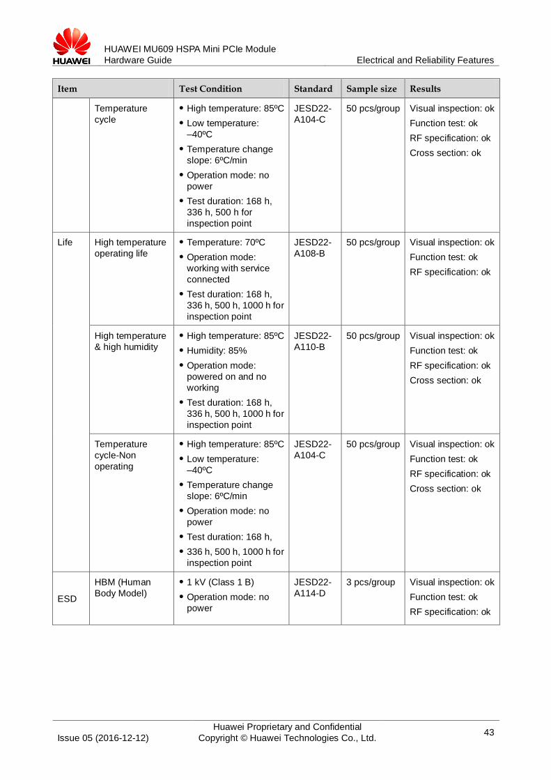
5.5 Reliability Features Table 5-9 lists the test conditions and results of the reliability of the MU609 module.
Table 5-9 Test conditions and results of the reliability of the MU609 module
Item Test Condition Standard Sample size Results
Stress Low-temperature
storage
Temperature: –40ºC
Operation mode: no
power, no package
Test duration: 24 h
JESD22-
A119-C
3 pcs/group Visual inspection: ok
Function test: ok
RF specification: ok
High-temperature
storage
Temperature: 85ºC
Operation mode: no
power, no package
Test duration: 24 h
JESD22-
A103-C
3 pcs/group Visual inspection: ok
Function test: ok
RF specification: ok
Low-temperature
operating
Temperature: –30ºC
Operation mode:
working with service
connected
Test duration: 24 h
IEC60068
-2-1
3 pcs/group Visual inspection: ok
Function test: ok
RF specification: ok
High-temperature
operating
Temperature: 70ºC
Operation mode:
working with service
connected
Test duration: 24 h
JESD22-
A108-C
3 pcs/group Visual inspection: ok
Function test: ok
RF specification: ok
Damp heat
cycling
High temperature: 55ºC
Low temperature: 25ºC
Humidity: 95%±3%
Operation mode:
working with service
connected
Test duration: 6 cycles;
12 h+12 h/cycle
JESD
22-A101-
B
3 pcs/group Visual inspection: ok
Function test: ok
RF specification: ok
Thermal shock Low temperature:
–40ºC
High temperature: 85ºC
Temperature change
interval: < 30s
Operation mode: no
power
Test duration: 100
cycles; 15 Min+15
Min/cycle
JESD22-
A106-B
3 pcs/group Visual inspection: ok
Function test: ok
RF specification: ok
HUAWEI MU609 HSPA Mini PCIe Module
Hardware Guide Electrical and Reliability Features
Issue 05 (2016-12-12)
Huawei Proprietary and Confidential
Copyright © Huawei Technologies Co., Ltd. 42
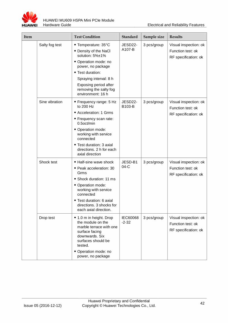
Item Test Condition Standard Sample size Results
Salty fog test Temperature: 35°C
Density of the NaCl
solution: 5%±1%
Operation mode: no
power, no package
Test duration:
Spraying interval: 8 h
Exposing period after
removing the salty fog
environment: 16 h
JESD22-
A107-B
3 pcs/group Visual inspection: ok
Function test: ok
RF specification: ok
Sine vibration Frequency range: 5 Hz
to 200 Hz
Acceleration: 1 Grms
Frequency scan rate:
0.5oct/min
Operation mode:
working with service
connected
Test duration: 3 axial
directions. 2 h for each
axial direction
JESD22-
B103-B
3 pcs/group Visual inspection: ok
Function test: ok
RF specification: ok
Shock test Half-sine wave shock
Peak acceleration: 30
Grms
Shock duration: 11 ms
Operation mode:
working with service
connected
Test duration: 6 axial
directions. 3 shocks for
each axial direction.
JESD-B1
04-C
3 pcs/group Visual inspection: ok
Function test: ok
RF specification: ok
Drop test 1.0 m in height. Drop
the module on the
marble terrace with one
surface facing
downwards. Six
surfaces should be
tested.
Operation mode: no
power, no package
IEC60068
-2-32
3 pcs/group Visual inspection: ok
Function test: ok
RF specification: ok
HUAWEI MU609 HSPA Mini PCIe Module
Hardware Guide Electrical and Reliability Features
Issue 05 (2016-12-12)
Huawei Proprietary and Confidential
Copyright © Huawei Technologies Co., Ltd. 43
Item Test Condition Standard Sample size Results
Temperature
cycle
High temperature: 85ºC
Low temperature:
–40ºC
Temperature change
slope: 6ºC/min
Operation mode: no
power
Test duration: 168 h,
336 h, 500 h for
inspection point
JESD22-
A104-C
50 pcs/group Visual inspection: ok
Function test: ok
RF specification: ok
Cross section: ok
Life High temperature
operating life
Temperature: 70ºC
Operation mode:
working with service
connected
Test duration: 168 h,
336 h, 500 h, 1000 h for
inspection point
JESD22-
A108-B
50 pcs/group Visual inspection: ok
Function test: ok
RF specification: ok
High temperature
& high humidity
High temperature: 85ºC
Humidity: 85%
Operation mode:
powered on and no
working
Test duration: 168 h,
336 h, 500 h, 1000 h for
inspection point
JESD22-
A110-B
50 pcs/group Visual inspection: ok
Function test: ok
RF specification: ok
Cross section: ok
Temperature
cycle-Non
operating
High temperature: 85ºC
Low temperature:
–40ºC
Temperature change
slope: 6ºC/min
Operation mode: no
power
Test duration: 168 h,
336 h, 500 h, 1000 h for
inspection point
JESD22-
A104-C
50 pcs/group Visual inspection: ok
Function test: ok
RF specification: ok
Cross section: ok
ESD
HBM (Human
Body Model)
1 kV (Class 1 B)
Operation mode: no
power
JESD22-
A114-D
3 pcs/group Visual inspection: ok
Function test: ok
RF specification: ok
HUAWEI MU609 HSPA Mini PCIe Module
Hardware Guide Electrical and Reliability Features
Issue 05 (2016-12-12)
Huawei Proprietary and Confidential
Copyright © Huawei Technologies Co., Ltd. 44
Item Test Condition Standard Sample size Results
ESD with DVK (or
embedded in the
host)
Contact and Air
discharges: 10 positive
and 10 negative
applied
Contact Voltage: ±2 kV,
±4 kV
Air Voltage : ±2 kV, ±4
kV, ±8 kV
Operation mode:
working with service
connected
IEC61000
-4-2
2 pcs Visual inspection: ok
Function test: ok
RF specification: ok
Groups ≥ 2
5.6 EMC and ESD Features The following are the EMC design comments:
Attention should be paid to static control in the manufacture, assembly, packaging, handling, storage process to reduce electrostatic damage to HUAWEI module.
RSE (Radiated Spurious Emission) may exceed the limit defined by EN301489 if the antenna port is protected by TVS (Transient Voltage Suppressor), which is resolved by making some adjustment on RF match circuit.
TVS should be added on the USB port for ESD protection, and the parasitic capacitance of TVS on D+/D- signal should be less than 2 pF. Common-mode inductor should be added in parallel on D+/D- signal.
TVS should be added on the USIM interface for ESD protection. The parasitic capacitance of TVS on USIM signal should be less than 10 pF.
Resistors in parallel and a 10 nF capacitor should be added on RESIN_N signal
to avoid shaking, and the distance between the capacitor and the related pin should be less than 100 mil.
PCB routing should be V-type rather than T-type for TVS.
An integrated ground plane is necessary for EMC design.
The following are the requirements of ESD environment control:
The electrostatic discharge protected area (EPA) must have an ESD floor whose surface resistance and system resistance are greater than 1 x 10
4 Ω while less
than 1 x 10⁹ Ω.
The EPA must have a sound ground system without loose ground wires, and the ground resistance must be less than 4 Ω.
The workbench for handling ESD sensitive components must be equipped with common ground points, the wrist strap jack, and ESD pad. The resistance between the jack and common ground point must be less than 4 Ω. The surface resistance and system resistance of the ESD pad must be less than 1 x 10
9 Ω.
HUAWEI MU609 HSPA Mini PCIe Module
Hardware Guide Electrical and Reliability Features
Issue 05 (2016-12-12)
Huawei Proprietary and Confidential
Copyright © Huawei Technologies Co., Ltd. 45
The EPA must use the ESD two-circuit wrist strap, and the wrist strap must be connected to the dedicated jack. The crocodile clip must not be connected to the ground.
The ESD sensitive components, the processing equipment, test equipment, tools, and devices must be connected to the ground properly. The indexes are as
follows:
− Hard ground resistance < 4 Ω
− 1 x 10⁵
Ω ≤ Soft ground resistance < 1 x 10⁹ Ω
− 1 x 10⁵ Ω ≤ ICT fixture soft ground resistance < 1 x 10
11 Ω
− The electronic screwdriver and electronic soldering iron can be easily oxidized. Their ground resistance must be less than 20 Ω.
The parts of the equipment, devices, and tools that touch the ESD sensitive components and moving parts that are close to the ESD sensitive components must be made of ESD materials and have sound ground connection. The parts that are not made of ESD materials must be handled with ESD treatment, such as painting the ESD coating or ionization treatment (check that the friction voltage
is less than 100 V).
Key parts in the production equipment (parts that touch the ESD sensitive components or parts that are within 30 cm away from the ESD sensitive components), including the conveyor belt, conveyor chain, guide wheel, and SMT nozzle, must all be made of ESD materials and be connected to the ground
properly (check that the friction voltage is less than 100 V).
Engineers that touch IC chips, boards, modules, and other ESD sensitive components and assemblies must wear ESD wrist straps, ESD gloves, or ESD finger cots properly. Engineers that sit when handling the components must all wear ESD wrist straps.
Noticeable ESD warning signs must be attached to the packages and placement
areas of ESD sensitive components and assemblies.
Boards and IC chips must not be stacked randomly or be placed with other ESD components.
Effective shielding measures must be taken on the ESD sensitive materials that are transported or stored outside the EPA.
HUAWEI MU609 Mini PCIe module does not include any protection against overvoltage.
HUAWEI MU609 HSPA Mini PCIe Module
Hardware Guide Mechanical Specifications
Issue 05 (2016-12-12)
Huawei Proprietary and Confidential
Copyright © Huawei Technologies Co., Ltd. 46
6 Mechanical Specifications
6.1 About This Chapter This chapter mainly describes mechanical specifications of MU609 module, including:
Dimensions and Interfaces
Dimensions of the Mini PCI Express Connector
Packaging
Label
Specification Selection for Fasteners
Antenna Plug
Thermal Design Guide
6.2 Dimensions and Interfaces
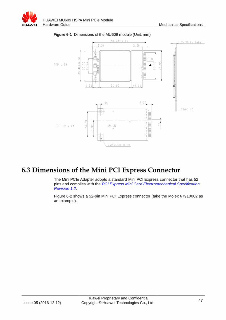
The dimensions of the MU609 module are 51 mm (length) × 30.4 mm (width) ×3.3 mm (height). Figure 6-1 shows the dimensions of MU609 module in detail.
Figure 6-1 shows the appearance of the interfaces on the MU609 module.
HUAWEI MU609 HSPA Mini PCIe Module
Hardware Guide Mechanical Specifications
Issue 05 (2016-12-12)
Huawei Proprietary and Confidential
Copyright © Huawei Technologies Co., Ltd. 47
Figure 6-1 Dimensions of the MU609 module (Unit: mm)
6.3 Dimensions of the Mini PCI Express Connector
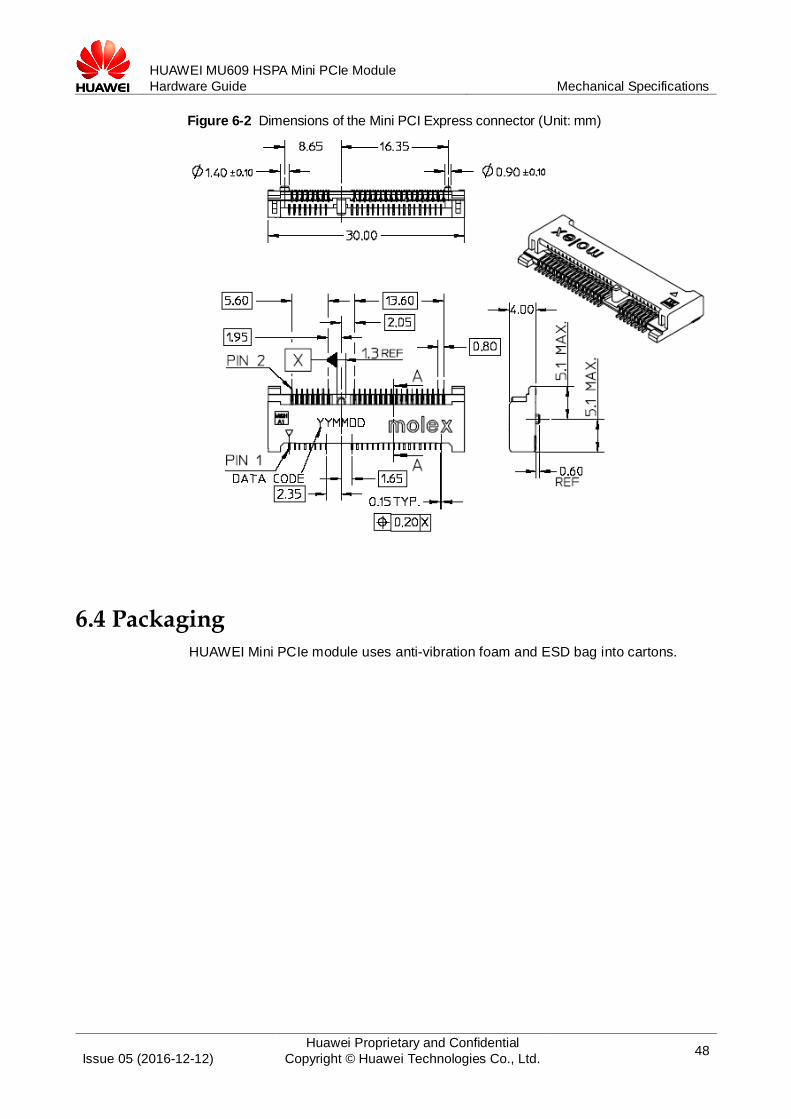
The Mini PCIe Adapter adopts a standard Mini PCI Express connector that has 52 pins and complies with the PCI Express Mini Card Electromechanical Specification Revision 1.2.
Figure 6-2 shows a 52-pin Mini PCI Express connector (take the Molex 67910002 as an example).
HUAWEI MU609 HSPA Mini PCIe Module
Hardware Guide Mechanical Specifications
Issue 05 (2016-12-12)
Huawei Proprietary and Confidential
Copyright © Huawei Technologies Co., Ltd. 48
Figure 6-2 Dimensions of the Mini PCI Express connector (Unit: mm)
6.4 Packaging
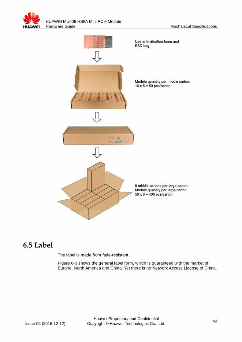
HUAWEI Mini PCIe module uses anti-vibration foam and ESD bag into cartons.
HUAWEI MU609 HSPA Mini PCIe Module
Hardware Guide Mechanical Specifications
Issue 05 (2016-12-12)
Huawei Proprietary and Confidential
Copyright © Huawei Technologies Co., Ltd. 49
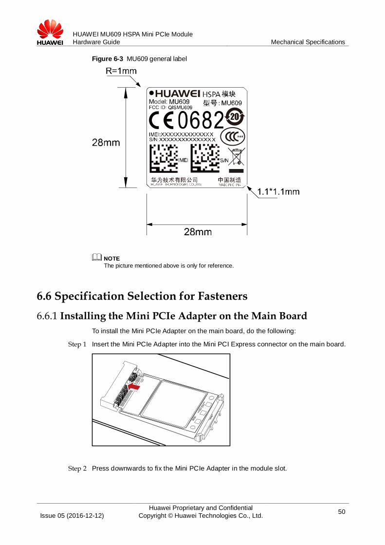
6.5 Label The label is made from fade-resistant.
Figure 6-3 shows the general label form, which is guaranteed with the market of Europe, North America and China. Yet there is no Network Access License of China.
HUAWEI MU609 HSPA Mini PCIe Module
Hardware Guide Mechanical Specifications
Issue 05 (2016-12-12)
Huawei Proprietary and Confidential
Copyright © Huawei Technologies Co., Ltd. 50
Figure 6-3 MU609 general label
The picture mentioned above is only for reference.
6.6 Specification Selection for Fasteners
6.6.1 Installing the Mini PCIe Adapter on the Main Board
To install the Mini PCIe Adapter on the main board, do the following:
Step 1 Insert the Mini PCIe Adapter into the Mini PCI Express connector on the main board.
Step 2 Press downwards to fix the Mini PCIe Adapter in the module slot.
HUAWEI MU609 HSPA Mini PCIe Module
Hardware Guide Mechanical Specifications
Issue 05 (2016-12-12)
Huawei Proprietary and Confidential
Copyright © Huawei Technologies Co., Ltd. 51
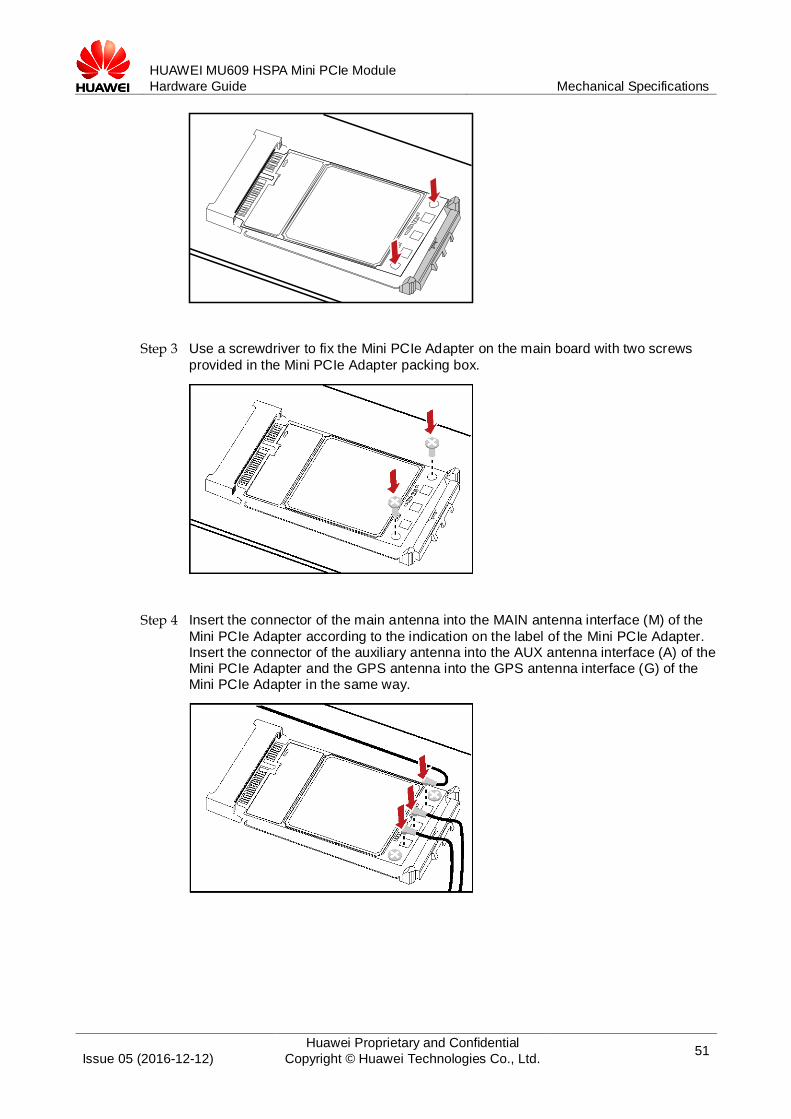
Step 3 Use a screwdriver to fix the Mini PCIe Adapter on the main board with two screws
provided in the Mini PCIe Adapter packing box.
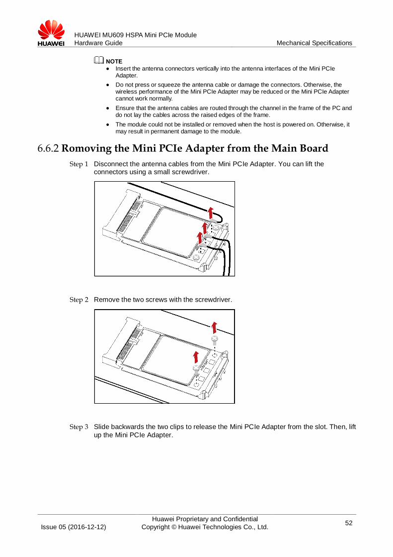
Step 4 Insert the connector of the main antenna into the MAIN antenna interface (M) of the
Mini PCIe Adapter according to the indication on the label of the Mini PCIe Adapter. Insert the connector of the auxiliary antenna into the AUX antenna interface (A) of the Mini PCIe Adapter and the GPS antenna into the GPS antenna interface (G) of the Mini PCIe Adapter in the same way.
HUAWEI MU609 HSPA Mini PCIe Module
Hardware Guide Mechanical Specifications
Issue 05 (2016-12-12)
Huawei Proprietary and Confidential
Copyright © Huawei Technologies Co., Ltd. 52
Insert the antenna connectors vertically into the antenna interfaces of the Mini PCIe
Adapter.
Do not press or squeeze the antenna cable or damage the connectors. Otherwise, the wireless performance of the Mini PCIe Adapter may be reduced or the Mini PCIe Adapter cannot work normally.
Ensure that the antenna cables are routed through the channel in the frame of the PC and do not lay the cables across the raised edges of the frame.
The module could not be installed or removed when the host is powered on. Otherwise, it may result in permanent damage to the module.
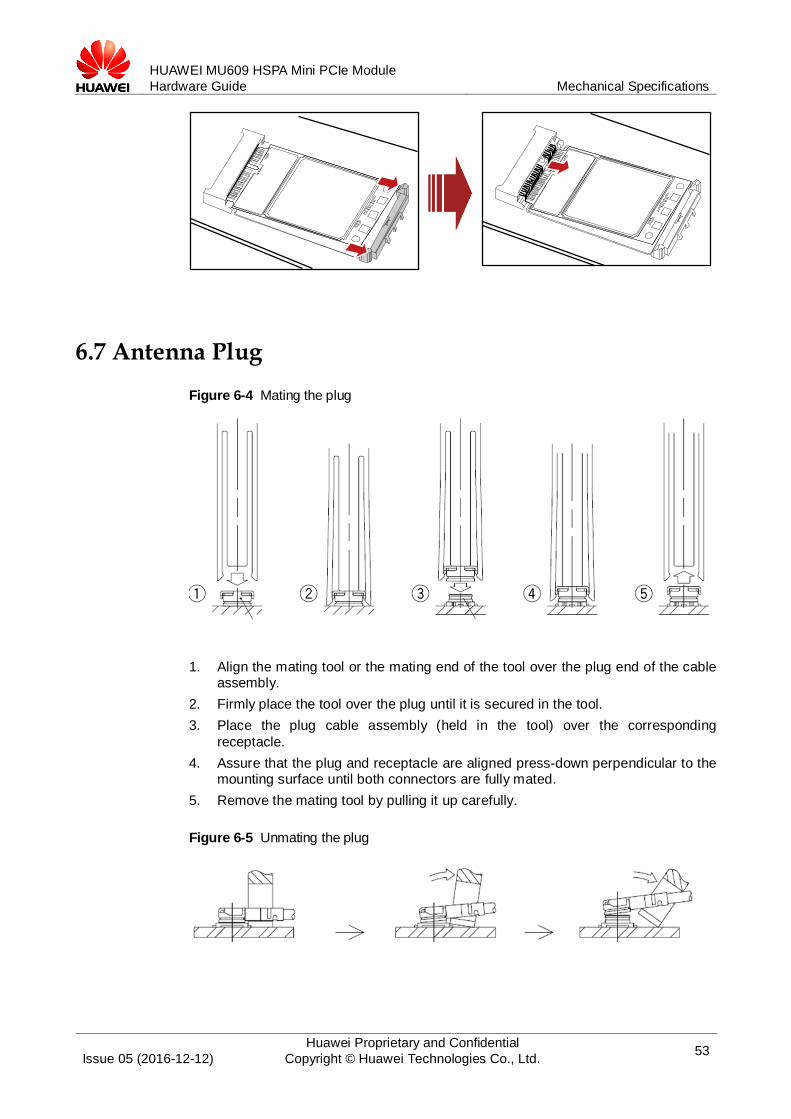
6.6.2 Romoving the Mini PCIe Adapter from the Main Board
Step 1 Disconnect the antenna cables from the Mini PCIe Adapter. You can lift the connectors using a small screwdriver.
Step 2 Remove the two screws with the screwdriver.
Step 3 Slide backwards the two clips to release the Mini PCIe Adapter from the slot. Then, lift
up the Mini PCIe Adapter.
HUAWEI MU609 HSPA Mini PCIe Module
Hardware Guide Mechanical Specifications
Issue 05 (2016-12-12)
Huawei Proprietary and Confidential
Copyright © Huawei Technologies Co., Ltd. 53
6.7 Antenna Plug
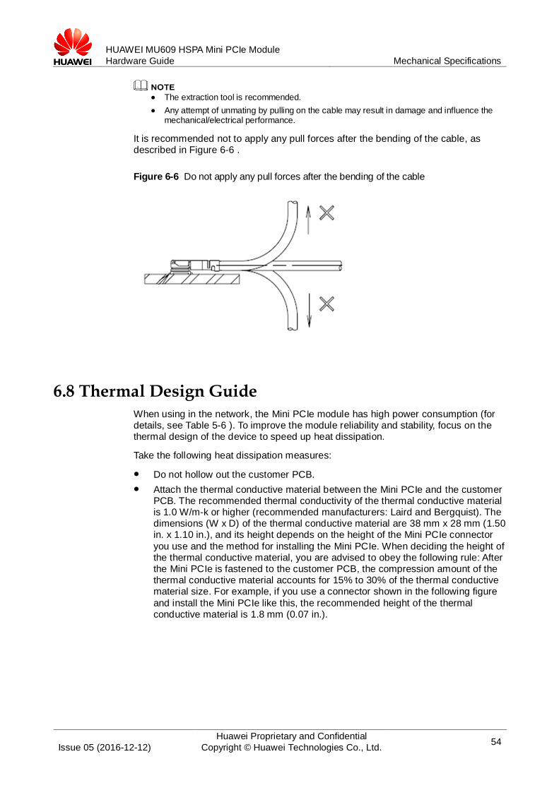
Figure 6-4 Mating the plug
1. Align the mating tool or the mating end of the tool over the plug end of the cable assembly.
2. Firmly place the tool over the plug until it is secured in the tool.
3. Place the plug cable assembly (held in the tool) over the corresponding
receptacle.
4. Assure that the plug and receptacle are aligned press-down perpendicular to the mounting surface until both connectors are fully mated.
5. Remove the mating tool by pulling it up carefully.
Figure 6-5 Unmating the plug
HUAWEI MU609 HSPA Mini PCIe Module
Hardware Guide Mechanical Specifications
Issue 05 (2016-12-12)
Huawei Proprietary and Confidential
Copyright © Huawei Technologies Co., Ltd. 54
The extraction tool is recommended.
Any attempt of unmating by pulling on the cable may result in damage and influence the mechanical/electrical performance.
It is recommended not to apply any pull forces after the bending of the cable, as described in Figure 6-6 .
Figure 6-6 Do not apply any pull forces after the bending of the cable
6.8 Thermal Design Guide When using in the network, the Mini PCIe module has high power consumption (for details, see Table 5-6 ). To improve the module reliability and stability, focus on the thermal design of the device to speed up heat dissipation.
Take the following heat dissipation measures:
Do not hollow out the customer PCB.
Attach the thermal conductive material between the Mini PCIe and the customer PCB. The recommended thermal conductivity of the thermal conductive material is 1.0 W/m-k or higher (recommended manufacturers: Laird and Bergquist). The dimensions (W x D) of the thermal conductive material are 38 mm x 28 mm (1.50 in. x 1.10 in.), and its height depends on the height of the Mini PCIe connector
you use and the method for installing the Mini PCIe. When deciding the height of the thermal conductive material, you are advised to obey the following rule: After the Mini PCIe is fastened to the customer PCB, the compression amount of the thermal conductive material accounts for 15% to 30% of the thermal conductive material size. For example, if you use a connector shown in the following figure
and install the Mini PCIe like this, the recommended height of the thermal conductive material is 1.8 mm (0.07 in.).
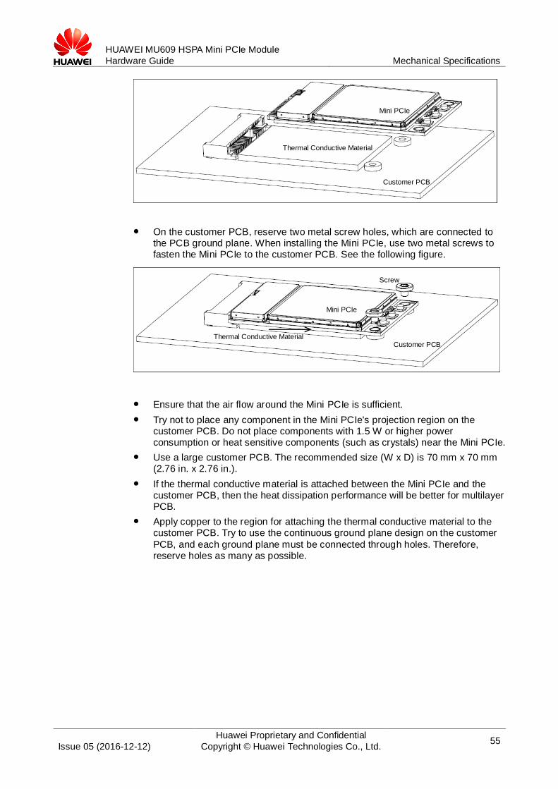
HUAWEI MU609 HSPA Mini PCIe Module
Hardware Guide Mechanical Specifications
Issue 05 (2016-12-12)
Huawei Proprietary and Confidential
Copyright © Huawei Technologies Co., Ltd. 55
On the customer PCB, reserve two metal screw holes, which are connected to the PCB ground plane. When installing the Mini PCIe, use two metal screws to fasten the Mini PCIe to the customer PCB. See the following figure.
Ensure that the air flow around the Mini PCIe is sufficient.
Try not to place any component in the Mini PCIe's projection region on the customer PCB. Do not place components with 1.5 W or higher power consumption or heat sensitive components (such as crystals) near the Mini PCIe.
Use a large customer PCB. The recommended size (W x D) is 70 mm x 70 mm (2.76 in. x 2.76 in.).
If the thermal conductive material is attached between the Mini PCIe and the customer PCB, then the heat dissipation performance will be better for multilayer PCB.
Apply copper to the region for attaching the thermal conductive material to the customer PCB. Try to use the continuous ground plane design on the customer
PCB, and each ground plane must be connected through holes. Therefore, reserve holes as many as possible.
Thermal Conductive Material
Thermal Conductive Material
Mini PCIe
Customer PCB
Screw
Mini PCIe
Customer PCB
HUAWEI MU609 HSPA Mini PCIe Module
Hardware Guide Certifications
Issue 05 (2016-12-12)
Huawei Proprietary and Confidential
Copyright © Huawei Technologies Co., Ltd. 56
7 Certifications
7.1 About This Chapter This chapter gives a general description of certifications of MU609 module.
7.2 Certifications
Table 7-1 shows certifications the MU609 module has been implemented. For more demands, please contact us for more details about this information.
Table 7-1 Product Certifications
Certification Model name
MU609
CE
FCC
CCC[1]
RoHS
WEEE
A-Tick
[1]: For CCC certification, the certification model is HUAWEI MU609.
HUAWEI MU609 HSPA Mini PCIe Module
Hardware Guide Safety Information
Issue 05 (2016-12-12)
Huawei Proprietary and Confidential
Copyright © Huawei Technologies Co., Ltd. 57
8 Safety Information
Read the safety information carefully to ensure the correct and safe use of your wireless device. Applicable safety information must be observed.
8.1 Interference Power off your wireless device if using the device is prohibited. Do not use the
wireless device when it causes danger or interference with electric devices.
8.2 Medical Device Power off your wireless device and follow the rules and regulations set forth by
the hospitals and health care facilities.
Some wireless devices may affect the performance of the hearing aids. For any
such problems, consult your service provider.
Pacemaker manufacturers recommend that a minimum distance of 15 cm be maintained between the wireless device and a pacemaker to prevent potential interference with the pacemaker. If you are using an electronic medical device, consult the doctor or device manufacturer to confirm whether the radio wave affects the operation of this device.
8.3 Area with Inflammables and Explosives To prevent explosions and fires in areas that are stored with inflammable and explosive devices, power off your wireless device and observe the rules. Areas stored with inflammables and explosives include but are not limited to the following:
Gas station
Fuel depot (such as the bunk below the deck of a ship)
Container/Vehicle for storing or transporting fuels or chemical products
Area where the air contains chemical substances and particles (such as granule, dust, or metal powder)
Area indicated with the "Explosives" sign
HUAWEI MU609 HSPA Mini PCIe Module
Hardware Guide Safety Information
Issue 05 (2016-12-12)
Huawei Proprietary and Confidential
Copyright © Huawei Technologies Co., Ltd. 58
Area indicated with the "Power off bi-direction wireless equipment" sign
Area where you are generally suggested to stop the engine of a vehicle
8.4 Traffic Security Observe local laws and regulations while using the wireless device. To prevent
accidents, do not use your wireless device while driving.
RF signals may affect electronic systems of motor vehicles. For more information, consult the vehicle manufacturer.
In a motor vehicle, do not place the wireless device over the air bag or in the air bag deployment area. Otherwise, the wireless device may hurt you owing to the strong force when the air bag inflates.
8.5 Airline Security Observe the rules and regulations of airline companies. When boarding or approaching a plane, power off your wireless device. Otherwise, the radio signal of the wireless device may interfere with the plane control signals.
8.6 Safety of Children
Do not allow children to use the wireless device without guidance. Small and sharp components of the wireless device may cause danger to children or cause suffocation if children swallow the components.
8.7 Environment Protection Observe the local regulations regarding the disposal of your packaging materials,
used wireless device and accessories, and promote their recycling.
8.8 WEEE Approval The wireless device is in compliance with the essential requirements and other relevant provisions of the Waste Electrical and Electronic Equipment Directive 2012/19/EU (WEEE Directive).
8.9 RoHS Approval The wireless device is in compliance with the restriction of the use of certain hazardous substances in electrical and electronic equipment Directive 2011/65/EU (RoHS Directive).
HUAWEI MU609 HSPA Mini PCIe Module
Hardware Guide Safety Information
Issue 05 (2016-12-12)
Huawei Proprietary and Confidential
Copyright © Huawei Technologies Co., Ltd. 59
8.10 Laws and Regulations Observance Observe laws and regulations when using your wireless device. Respect the privacy and legal rights of the others.
8.11 Care and Maintenance It is normal that your wireless device gets hot when you use or charge it. Before you
clean or maintain the wireless device, stop all applications and power off the wireless device.
Use your wireless device and accessories with care and in clean environment. Keep the wireless device from a fire or a lit cigarette.
Protect your wireless device and accessories from water and vapour and keep
them dry.
Do not drop, throw or bend your wireless device.
Clean your wireless device with a piece of damp and soft antistatic cloth. Do not use any chemical agents (such as alcohol and benzene), chemical detergent, or powder to clean it.
Do not leave your wireless device and accessories in a place with a considerably low or high temperature.
Use only accessories of the wireless device approved by the manufacture. Contact the authorized service center for any abnormity of the wireless device or accessories.
Do not dismantle the wireless device or accessories. Otherwise, the wireless
device and accessories are not covered by the warranty.
The device should be installed and operated with a minimum distance of 20 cm between the radiator and your body.
8.12 Emergency Call This wireless device functions through receiving and transmitting radio signals.
Therefore, the connection cannot be guaranteed in all conditions. In an emergency, you should not rely solely on the wireless device for essential communications.
8.13 Regulatory Information The following approvals and notices apply in specific regions as noted.
8.13.1 CE Approval (European Union)
The wireless device is approved to be used in the member states of the EU. The
wireless device is in compliance with the essential requirements and other relevant provisions of the Radio and Telecommunications Terminal Equipment Directive 1999/5/EC (R&TTE Directive).
HUAWEI MU609 HSPA Mini PCIe Module
Hardware Guide Safety Information
Issue 05 (2016-12-12)
Huawei Proprietary and Confidential
Copyright © Huawei Technologies Co., Ltd. 60
8.13.2 FCC Statement
Federal Communications Commission Notice (United States): Before a wireless device model is available for sale to the public, it must be tested and certified to the FCC that it does not exceed the limit established by the government-adopted requirement for safe exposure.
This device complies with Part 15 of the FCC Rules. Operation is subject to the
following two conditions: (1) this device may not cause harmful interference, and (2) this device must accept any interference received, including interference that may cause undesired operation.
Warning: Changes or modifications made to this equipment not expressly approved by HUAWEI may void the FCC authorization to operate this equipment.
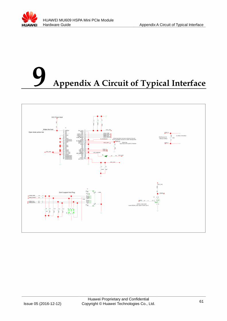
HUAWEI MU609 HSPA Mini PCIe Module
Hardware Guide Appendix A Circuit of Typical Interface
Issue 05 (2016-12-12)
Huawei Proprietary and Confidential
Copyright © Huawei Technologies Co., Ltd. 61
9 Appendix A Circuit of Typical Interface 150uF
C5
C6
33pF
R1
10K
D1 R2 470
J2
11
736
251
4
10
9
8S2
S3
M1
CD
VCCGNDRST
VPPCLKI/O
M2
R3 0
R4 0
R5 0R6 0
D2
61 3
4
25
1uF
C8
33pF
C9
150uF
C3
33pF
C10
33pF
C11
33pF
C12
Q1
2
3
1G
D
S
C1
100nF
R7 0
R8
100K
J1
24
13579
111315171921232527293133353739414345474951
246810121416182022
2628303234363840424446485052
VCC_3V3GND13
NCNCNC
LED_WWAN#GND12
USB_DPUSB_DM
GND9NCNCNC
GND6
RESIN_NW_DISABLE#
GND4NC
USIM_RESETUSIM_CLK
USIM_DATAUSIM_PWR
NCGND1
VCC_3V3
RESERVED6RESERVED5RESERVED4RESERVED3GND13VCC_3V3VCC_3V3GND11GND10NCNCGND8GND7NCNCGND5RESERVED2RESERVED1GND3NCNCGND2NCNCNCWAKE#
VCC_3V3
C2
10pF
C4
150uF
C7
1.8
pF
GND
GND
USB_D+
USB_D+
USIM_DATA
USIM_DATA
USIM_CLK
USIM_CLK
USIM_RESET
USIM_RESET
USIM_PWR
USIM_PWR
W_DISABLE#
LED_WWAN#
USB_D-
USB_D-
VCC_3V3
VCC_3V3
VCC_3V3
VCC_3V3
VCC_3V3
VCC_3V3
RESIN_N
RESIN_N
GPIO1
Wake the host
VCC From Host
Cap close to the pin22 of moduleActive low
Active low (Don't connect a diode to this pin) DNIDNI,Reserve for
USB eye debug
GPIO1 is from SOC
Leave RESIN_N pin open if donot use it.
to USB 2.0 interface
Open drain,active low
The W_DISABLE function is under development.
Don't support Hot Plug.
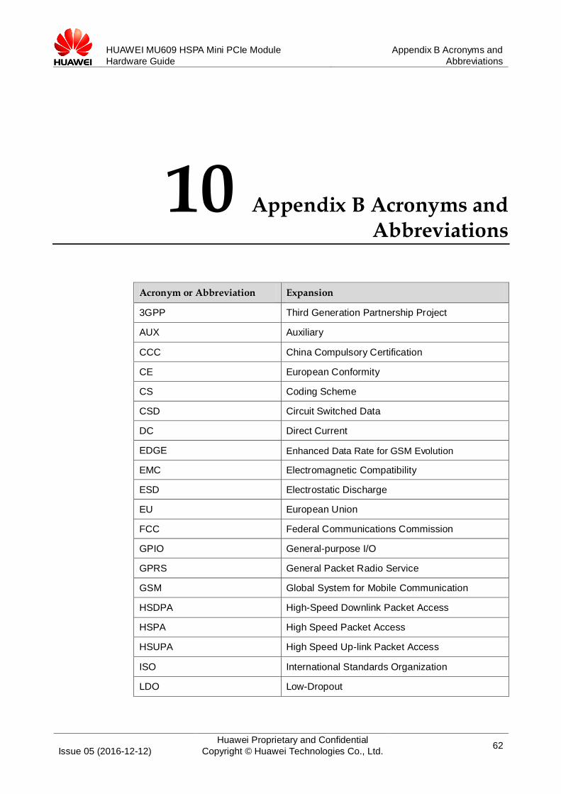
HUAWEI MU609 HSPA Mini PCIe Module
Hardware Guide
Appendix B Acronyms and
Abbreviations
Issue 05 (2016-12-12)
Huawei Proprietary and Confidential
Copyright © Huawei Technologies Co., Ltd. 62
10 Appendix B Acronyms and Abbreviations
Acronym or Abbreviation Expansion
3GPP Third Generation Partnership Project
AUX Auxiliary
CCC China Compulsory Certification
CE European Conformity
CS Coding Scheme
CSD Circuit Switched Data
DC Direct Current
EDGE Enhanced Data Rate for GSM Evolution
EMC Electromagnetic Compatibility
ESD Electrostatic Discharge
EU European Union
FCC Federal Communications Commission
GPIO General-purpose I/O
GPRS General Packet Radio Service
GSM Global System for Mobile Communication
HSDPA High-Speed Downlink Packet Access
HSPA High Speed Packet Access
HSUPA High Speed Up-link Packet Access
ISO International Standards Organization
LDO Low-Dropout
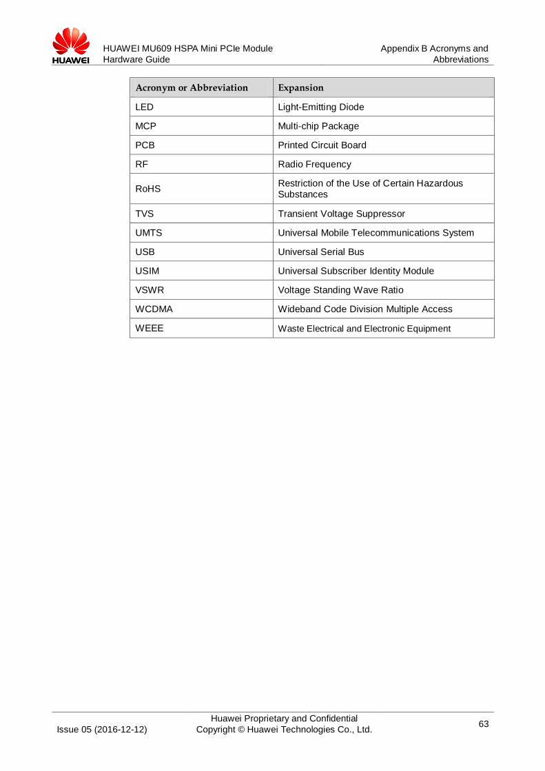
HUAWEI MU609 HSPA Mini PCIe Module
Hardware Guide
Appendix B Acronyms and
Abbreviations
Issue 05 (2016-12-12)
Huawei Proprietary and Confidential
Copyright © Huawei Technologies Co., Ltd. 63
Acronym or Abbreviation Expansion
LED Light-Emitting Diode
MCP Multi-chip Package
PCB Printed Circuit Board
RF Radio Frequency
RoHS Restriction of the Use of Certain Hazardous Substances
TVS Transient Voltage Suppressor
UMTS Universal Mobile Telecommunications System
USB Universal Serial Bus
USIM Universal Subscriber Identity Module
VSWR Voltage Standing Wave Ratio
WCDMA Wideband Code Division Multiple Access
WEEE Waste Electrical and Electronic Equipment