Embed Size (px)
Citation preview

HW-CLK-101-SCLK2 SuperClock-2 Module
User Guide
UG770 (v1.0) September 23, 2010

SuperClock-2 Module User Guide www.xilinx.com UG770 (v1.0) September 23, 2010
Xilinx is disclosing this user guide, manual, release note, and/or specification (the “Documentation”) to you solely for use in the development of designs to operate with Xilinx hardware devices. You may not reproduce, distribute, republish, download, display, post, or transmit the Documentation in any form or by any means including, but not limited to, electronic, mechanical, photocopying, recording, or otherwise, without the prior written consent of Xilinx. Xilinx expressly disclaims any liability arising out of your use of the Documentation. Xilinx reserves the right, at its sole discretion, to change the Documentation without notice at any time. Xilinx assumes no obligation to correct any errors contained in the Documentation, or to advise you of any corrections or updates. Xilinx expressly disclaims any liability in connection with technical support or assistance that may be provided to you in connection with the Information.
THE DOCUMENTATION IS DISCLOSED TO YOU “AS-IS” WITH NO WARRANTY OF ANY KIND. XILINX MAKES NO OTHER WARRANTIES, WHETHER EXPRESS, IMPLIED, OR STATUTORY, REGARDING THE DOCUMENTATION, INCLUDING ANY WARRANTIES OF MERCHANTABILITY, FITNESS FOR A PARTICULAR PURPOSE, OR NONINFRINGEMENT OF THIRD-PARTY RIGHTS. IN NO EVENT WILL XILINX BE LIABLE FOR ANY CONSEQUENTIAL, INDIRECT, EXEMPLARY, SPECIAL, OR INCIDENTAL DAMAGES, INCLUDING ANY LOSS OF DATA OR LOST PROFITS, ARISING FROM YOUR USE OF THE DOCUMENTATION.
© Copyright 2010 Xilinx, Inc. XILINX, the Xilinx logo, Virtex, Spartan, ISE, and other designated brands included herein are trademarks of Xilinx in the United States and other countries. All other trademarks are the property of their respective owners.
Revision HistoryThe following table shows the revision history for this document.
Date Version Revision
09/23/10 1.0 Initial Xilinx release.

SuperClock-2 Module User Guide www.xilinx.com 3UG770 (v1.0) September 23, 2010
Revision History . . . . . . . . . . . . . . . . . . . . . . . . . . . . . . . . . . . . . . . . . . . . . . . . . . . . . . . . . . . . . 2
Preface: About This GuideAdditional Resources . . . . . . . . . . . . . . . . . . . . . . . . . . . . . . . . . . . . . . . . . . . . . . . . . . . . . . . . 5Technical Support. . . . . . . . . . . . . . . . . . . . . . . . . . . . . . . . . . . . . . . . . . . . . . . . . . . . . . . . . . . . 5Conventions . . . . . . . . . . . . . . . . . . . . . . . . . . . . . . . . . . . . . . . . . . . . . . . . . . . . . . . . . . . . . . . . . 6
Typographical . . . . . . . . . . . . . . . . . . . . . . . . . . . . . . . . . . . . . . . . . . . . . . . . . . . . . . . . . . . . . 6Online Document . . . . . . . . . . . . . . . . . . . . . . . . . . . . . . . . . . . . . . . . . . . . . . . . . . . . . . . . . . 6
HW-CLK-101-SCLK2SuperClock-2 Module
SuperClock-2 Module Features . . . . . . . . . . . . . . . . . . . . . . . . . . . . . . . . . . . . . . . . . . . . . . . 8I2C Interface . . . . . . . . . . . . . . . . . . . . . . . . . . . . . . . . . . . . . . . . . . . . . . . . . . . . . . . . . . . . . . 8
Detailed Description . . . . . . . . . . . . . . . . . . . . . . . . . . . . . . . . . . . . . . . . . . . . . . . . . . . . . . . . . 8Host Interface Connector . . . . . . . . . . . . . . . . . . . . . . . . . . . . . . . . . . . . . . . . . . . . . . . . . . 10114.285 MHz Crystal . . . . . . . . . . . . . . . . . . . . . . . . . . . . . . . . . . . . . . . . . . . . . . . . . . . . . . 14External Input Clock SMA Pair . . . . . . . . . . . . . . . . . . . . . . . . . . . . . . . . . . . . . . . . . . . . . 14Si570 Clock Out SMA Pair . . . . . . . . . . . . . . . . . . . . . . . . . . . . . . . . . . . . . . . . . . . . . . . . . 14Si5368 Clock Out SMA Pairs . . . . . . . . . . . . . . . . . . . . . . . . . . . . . . . . . . . . . . . . . . . . . . . 14Si5368 Jitter Attenuator and Clock Multiplier . . . . . . . . . . . . . . . . . . . . . . . . . . . . . . . . . 15ST2378 Level Translators . . . . . . . . . . . . . . . . . . . . . . . . . . . . . . . . . . . . . . . . . . . . . . . . . . 17Status LEDS. . . . . . . . . . . . . . . . . . . . . . . . . . . . . . . . . . . . . . . . . . . . . . . . . . . . . . . . . . . . . . 18
Loss of Lock . . . . . . . . . . . . . . . . . . . . . . . . . . . . . . . . . . . . . . . . . . . . . . . . . . . . . . . . . . 18Alarm . . . . . . . . . . . . . . . . . . . . . . . . . . . . . . . . . . . . . . . . . . . . . . . . . . . . . . . . . . . . . . . 18
NB6L11 Differential Buffer . . . . . . . . . . . . . . . . . . . . . . . . . . . . . . . . . . . . . . . . . . . . . . . . . 18Si570 Programmable Oscillator . . . . . . . . . . . . . . . . . . . . . . . . . . . . . . . . . . . . . . . . . . . . . 18Oscillator Inhibit. . . . . . . . . . . . . . . . . . . . . . . . . . . . . . . . . . . . . . . . . . . . . . . . . . . . . . . . . . 19
Installing the SuperClock-2 Module . . . . . . . . . . . . . . . . . . . . . . . . . . . . . . . . . . . . . . . . . 19References . . . . . . . . . . . . . . . . . . . . . . . . . . . . . . . . . . . . . . . . . . . . . . . . . . . . . . . . . . . . . . . . . . 19
Table of Contents

4 www.xilinx.com SuperClock-2 Module User GuideUG770 (v1.0) September 23, 2010

SuperClock-2 Module User Guide www.xilinx.com 5UG770 (v1.0) September 23, 2010
Preface
About This Guide
This document describes the features and operation of the HW-CLK-101-SCLK2 SuperClock-2 module. The SuperClock-2 module is a plug-in board that provides a programmable, low-noise and low-jitter clock source for Xilinx® transceiver characterization boards including:
• ML628 Virtex®-6 FPGA GTX and GTH transceiver characterization board
• ML623 Virtex-6 FPGA GTX transceiver characterization board
• SP623 Spartan®-6 FPGA GTP transceiver characterization board
Additional ResourcesTo find additional documentation, see the Xilinx website at:
http://www.xilinx.com/support/documentation/index.htm.
To search the Answer Database of silicon, software, and IP questions and answers, or to create a technical support WebCase, see the Xilinx website at:
http://www.xilinx.com/support.
To find Information about the ISE® Design Suite, see the Xilinx website at:
www.xilinx.com/ise
To find Information about intellectual property, see the Xilinx website at:
www.xilinx.com/ipcenter
Characterization board documentation, schematics and PCB design files are available at
www.xilinx.com/support/documentation/board_and_kit_documentation.htm.
Technical SupportXilinx offers technical support for the SuperClock-2 module when used in conjunction with the characterization boards listed here:
• ML628 Virtex-6 FPGA GTX and GTH transceiver characterization board
• ML623 Virtex-6 FPGA GTX transceiver characterization board
• SP623 Spartan-6 FPGA GTP transceiver characterization board
For assistance, see the Xilinx website at:
www.xilinx.com/support.
6 www.xilinx.com SuperClock-2 Module User GuideUG770 (v1.0) September 23, 2010
Preface: About This Guide
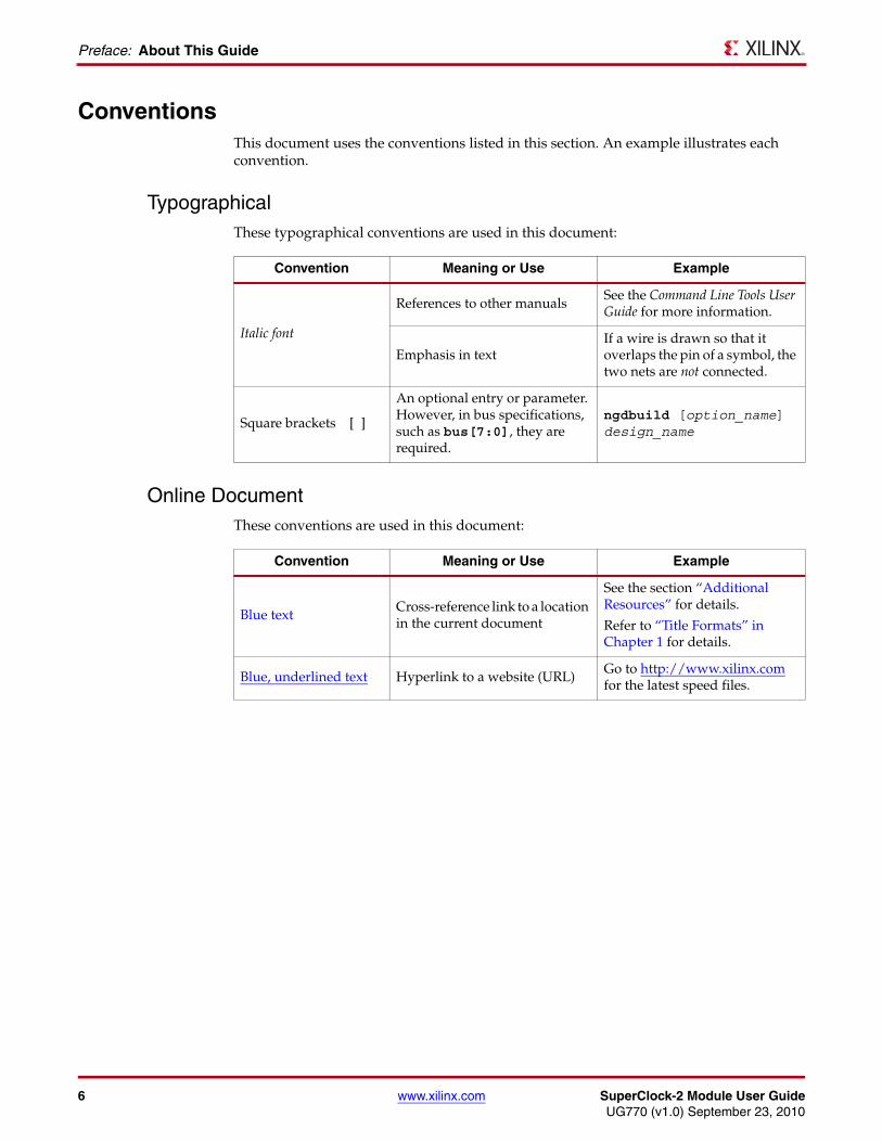
ConventionsThis document uses the conventions listed in this section. An example illustrates each convention.
TypographicalThese typographical conventions are used in this document:
Online DocumentThese conventions are used in this document:
Convention Meaning or Use Example
Italic font
References to other manualsSee the Command Line Tools User Guide for more information.
Emphasis in textIf a wire is drawn so that it overlaps the pin of a symbol, the two nets are not connected.
Square brackets [ ]
An optional entry or parameter. However, in bus specifications, such as bus[7:0], they are required.
ngdbuild [option_name] design_name
Convention Meaning or Use Example
Blue textCross-reference link to a location in the current document
See the section “Additional Resources” for details.
Refer to “Title Formats” in Chapter 1 for details.
Blue, underlined text Hyperlink to a website (URL) Go to http://www.xilinx.com for the latest speed files.

SuperClock-2 Module User Guide www.xilinx.com 7UG770 (v1.0) September 23, 2010
HW-CLK-101-SCLK2SuperClock-2 Module
The HW-CLK-101-SCLK2 SuperClock-2 module is a precision clock multiplier with sub- 1 ps rms jitter performance for use with Xilinx® transceiver characterization boards including:
• ML628 Virtex®-6 FPGA GTX and GTH transceiver characterization board
• ML623 Virtex-6 FPGA GTX transceiver characterization board
• SP623 Spartan®-6 FPGA GTP transceiver characterization board
The SuperClock-2 module (Figure 1) provides five independent clock outputs and can select any of three input clock sources as the reference for an internal digital clock oscillator (DCO). The output clocks can be programmed for any frequency in the range from 2 kHz to 808 MHz. TheSuperClock-2 module has no onboard voltage regulators. Power (3.3VDC) is provided through the host interface connector J1.
X-Ref Target - Figure 1-1
Figure 1: SuperClock-2 Module Block Diagram
UG770_C1_01_090810
Loss of LockAlarm
LEDs
NB6L111:2
Splitter
Crystal(114.285 MHz)
Si570Programmable
Oscillator(156.25 MHz
Default)
ST2378Level Translators
3V3
Si5368 Clock Multiplier/Jitter Attenuator
SMA
2
SMA
2
SMA
2
SMA
2
SMA
2
SMA
2
2
2
2
1313
3V3
3V3
3V3 3V3
SamtecQSH-060
Host InterfaceConnector
(J1)
VCC2V5
VCCO
VCC3V3
Digital Control
CLKOUT1
CLKOUT2
CLKOUT3
CLKOUT4
LOL/ALRM
XA/XB
SCL/SDA
CKIN1
CKIN3
CKOUT/FSOUT
VDD
CKIN4
VL
VCC
I2C Bus
CKIN2
Si570_CLK
CM_LVDS1_P/N
CM_LVDS2_P/N
CM_GCLK_P/N (Frame Sync Out)
EXT_CLK
1
2
J18

8 www.xilinx.com SuperClock-2 Module User GuideUG770 (v1.0) September 23, 2010
SuperClock-2 Module Features
SuperClock-2 Module Features• Compatible with Virtex-6 GTX and GTH characterization boards
• Compatible with Spartan-6 GTP characterization boards
• LEDs indicate loss of lock and programmable alarm conditions
• Programmable crystal oscillator (Silicon Laboratories Si570):
• I2C serial interface
• Programmable to any output frequency from 10 MHz to 810 MHz
• 156.25 MHz default frequency
• One LVDS output clock to SMA pair
• Jitter performance: less than 1 ps RMS
• Any-rate precision clock multiplier/jitter attenuator (Silicon Laboratories Si5368):
• I2C serial interface
• Programmable to any output frequency from 2 kHz to 808 MHz
• One LVDS input clock from SMA pair
• Two LVDS input clocks via host interface connector
• Four LVDS output clocks to SMA pairs
• One LVDS output clock to host interface connector
• Jitter performance: Less than 1 ps RMS
I2C InterfaceThe Si570 Programmable crystal oscillator and the Si5368 clock generator/jitter attenuator are slave devices sharing the same I2C bus. Pull-up resistors for the serial data a clock lines are located on the host characterization board only. Both devices support fast mode up to 400 kbps. The I2C idcodes for each device are listed in Table 1.
Detailed DescriptionFigure 2 shows the SuperClock-2 module. Each numbered feature that is referenced in the figure is described in the sections that follow.
Note: The image in Figure 2 is for reference and might not reflect the current revision of the module.
Table 1: I2C Device idcodes
DeviceI2C idcode
(Hex)I2C idcode(Decimal)
Si570 0x55 85
Si5368 0x68 104

SuperClock-2 Module User Guide www.xilinx.com 9UG770 (v1.0) September 23, 2010
Detailed Description
UG770_c1_02_090910
2
1
109
3 4 5 86 7 5
11
X-Ref Target - Figure 2
Figure 2: SuperClock-2 Module Features
1 SAMTEC 120-pin QSH host interface connector (J1): J1 provides power from host board, digital control signals and LVDS clocks.
2 114.285 MHz Crystal (X1): X1 is the fixed frequency reference for the Si5368 programmable crystal oscillator.
3 External clock SMA pair (J3/J4): J3 and J4 are connectors for an LVDS input clock. These signals are AC coupled and routed to the Si5368 clock multiplier/jitter attenuator.
4 Si570 programmable crystal oscillator clock out SMA pair (J13/J14): This output is a buffered copy of the Si570 programmable oscillator.
5 Si5368 clock output SMA pairs (J5/J6, J7/J8, J17/J12, J15/J18): CLK_OUT1 through CLK_OUT4 provide four LVDS clock output pairs from the Si5368 any-rate precision clock multiplier/jitter attenuator.
6 Si5368 any-rate precision clock multiplier/jitter attenuator (U5): Provides the clock for CLK_OUT1 through CLK_OUT4.
7 ST2378 level translators (U1, U2) and host voltage source selection header (J18): U1 and U2 convert the variable I/O control voltage from the host board to the 3.3V logic levels used by the SuperClock-2 module. The position of the jumper on J18 selects translation from either 2.5V or VCCO logic levels.
8 Status LEDS (DS1 and DS2): When illuminated, DS1 indicates loss of lock and DS2 indicates a programmable ALARM condition is active.
9 NB6L11 1:2 differential clock buffer/splitter (U4): U4 splits and buffers the Si570 clock output for the Si5368 CKIN2 input and the Si570_CLK SMA pair.
10 Si570 programmable crystal oscillator (U3): U3 is one of the clock sources for the Si5368.
11 Si570 programmable crystal oscillator clock output enable selection header (J11): Installing a jumper at J11 disables the oscillator.

10 www.xilinx.com SuperClock-2 Module User GuideUG770 (v1.0) September 23, 2010
Detailed Description
Host Interface Connector[Figure 2, callout 1]
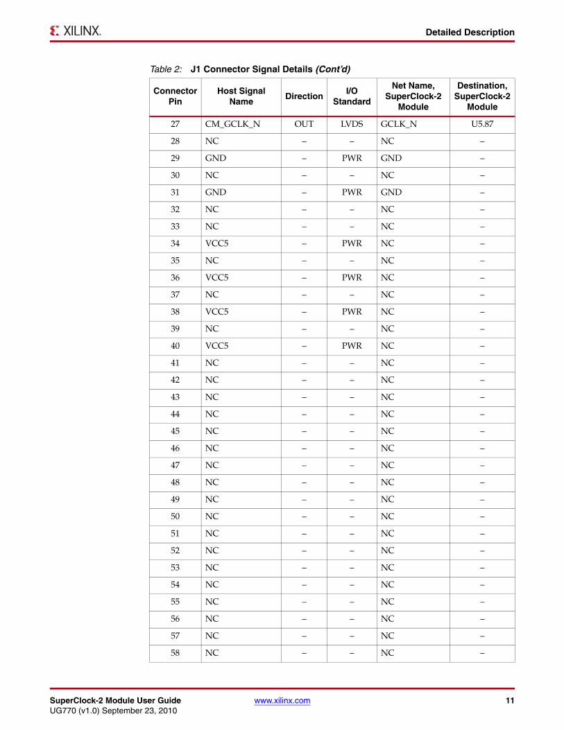
The SuperClock-2 module mates with the host transceiver board using a low profile, 120-pin, high-speed SAMTEC QTS connector. The connector has interior ground blades that are listed as pin 121 through pin 128 in Table 2. For flexibility, the host transceiver board provides three voltage rails on the connector: 2.5 VDC, 3.3 VDC and 5.0VDC.
Table 2: J1 Connector Signal Details
ConnectorPin
Host SignalName
DirectionI/O
Standard
Net Name,SuperClock-2
Module
Destination,SuperClock-2
Module
1 CM_LVDS1_P IN LVDS LVDS1_P(1) U5.44
2 VCC3V3 – PWR VCC3V3 –
3 CM_LVDS1_N IN LVDS LVDS1_N(1) U5.45
4 VCC3V3 – PWR VCC3V3 –
5 GND – PWR GND –
6 VCC3V3 – PWR VCC3V3 –
7 GND – PWR GND –
8 VCC3V3 – PWR VCC3V3 –
9 CM_LVDS2_P IN LVDS LVDS2_P(1) U5.39
10 NC – – NC –
11 CM_LVDS2_N IN LVDS LVDS2_N(1) U5.40
12 NC – – NC –
13 GND – PWR GND –
14 NC – – NC –
15 GND – PWR GND –
16 NC – – NC –
17 CM_LVDS3_P(2) IN LVDS NC –
18 VCC2V5 – PWR VCC2V5 –
19 CM_LVDS3_N(2) IN LVDS NC –
20 VCC2V5 – PWR VCC2V5 –
21 GND – PWR GND –
22 VCC2V5 – PWR VCC2V5 –
23 GND – PWR GND –
24 VCC2V5 – PWR VCC2V5 –
25 CM_GCLK_P OUT LVDS GCLK_P U5.88
26 NC – – NC –
SuperClock-2 Module User Guide www.xilinx.com 11UG770 (v1.0) September 23, 2010
Detailed Description
27 CM_GCLK_N OUT LVDS GCLK_N U5.87
28 NC – – NC –
29 GND – PWR GND –
30 NC – – NC –
31 GND – PWR GND –
32 NC – – NC –
33 NC – – NC –
34 VCC5 – PWR NC –
35 NC – – NC –
36 VCC5 – PWR NC –
37 NC – – NC –
38 VCC5 – PWR NC –
39 NC – – NC –
40 VCC5 – PWR NC –
41 NC – – NC –
42 NC – – NC –
43 NC – – NC –
44 NC – – NC –
45 NC – – NC –
46 NC – – NC –
47 NC – – NC –
48 NC – – NC –
49 NC – – NC –
50 NC – – NC –
51 NC – – NC –
52 NC – – NC –
53 NC – – NC –
54 NC – – NC –
55 NC – – NC –
56 NC – – NC –
57 NC – – NC –
58 NC – – NC –
Table 2: J1 Connector Signal Details (Cont’d)
ConnectorPin
Host SignalName
DirectionI/O
Standard
Net Name,SuperClock-2
Module
Destination,SuperClock-2
Module

12 www.xilinx.com SuperClock-2 Module User GuideUG770 (v1.0) September 23, 2010
Detailed Description
59 NC – – NC –
60 NC – – NC –
61 CM_CTRL_0 – LVCMOS NC –
62 CM_I2C_SCL IN LVCMOS I2C_SCL U3.8 / U5.60
63 CM_CTRL_1 – LVCMOS NC –
64 CM_I2C_SDA BI LVCMOS I2C_SDA U3.7 / U5.61
65 CM_CTRL_2 – LVCMOS NC –
66 CM_RST IN LVCMOS H_RESET_B U1.2
67 CM_CTRL_3 IN LVCMOS H_DEC U1.16
68 NC – – NC –
69 CM_CTRL_4 IN LVCMOS H_INC U1.6
70 NC – – NC –
71 CM_CTRL_5 IN LVCMOS H_FS_ALIGN U2.12
72 NC – – NC –
73 CM_CTRL_6 – LVCMOS NC –
74 NC – – NC –
75 CM_CTRL_7 – LVCMOS NC –
76 NC – – NC –
77 CM_CTRL_8 – LVCMOS NC –
78 NC – – NC –
79 CM_CTRL_9 OUT LVCMOS H_LOL U2.2
80 NC – – NC –
81 CM_CTRL_10 OUT LVCMOS H_INT_ALRM U2.18
82 NC – – NC –
83 CM_CTRL_11 OUT LVCMOS H_C1B U2.4
84 NC – – NC –
85 CM_CTRL_12 OUT LVCMOS H_C2B U2.16
86 NC – – NC –
87 CM_CTRL_13 OUT LVCMOS H_C3B U2.6
88 NC – – NC –
89 CM_CTRL_14 OUT LVCMOS H_C1A U2.14
90 NC – – NC –
Table 2: J1 Connector Signal Details (Cont’d)
ConnectorPin
Host SignalName
DirectionI/O
Standard
Net Name,SuperClock-2
Module
Destination,SuperClock-2
Module

SuperClock-2 Module User Guide www.xilinx.com 13UG770 (v1.0) September 23, 2010
Detailed Description
91 CM_CTRL_15 OUT LVCMOS H_C2A U2.8
92 NC – – NC –
93 CM_CTRL_16 – LVCMOS NC –
94 NC – – NC –
95 CM_CTRL_17 BI LVCMOS H_CS0_C3A U1.8
96 NC – – NC –
97 CM_CTRL_18 BI LVCMOS H_CS1_C4A U1.12
98 NC – – NC –
99 CM_CTRL_19 – LVCMOS NC –
100 NC – – NC –
101 CM_CTRL_20 – LVCMOS NC –
102 NC – – NC –
103 CM_CTRL_21 – LVCMOS NC –
104 NC – – NC –
105 CM_CTRL_22 – LVCMOS NC –
106 NC – – NC –
107 CM_CTRL_23 – LVCMOS NC –
108 NC – – NC –
109 NC – – NC –
110 NC – – NC –
111 NC – – NC –
112 NC – – NC –
113 NC – – NC –
114 NC – – NC –
115 NC – – NC –
116 NC – – NC –
117 NC – – NC –
118 NC – – NC –
119 NC – – NC –
120 NC – – NC –
121 GND(3) – PWR GND –
122 GND(3) – PWR GND –
Table 2: J1 Connector Signal Details (Cont’d)
ConnectorPin
Host SignalName
DirectionI/O
Standard
Net Name,SuperClock-2
Module
Destination,SuperClock-2
Module

14 www.xilinx.com SuperClock-2 Module User GuideUG770 (v1.0) September 23, 2010
Detailed Description
114.285 MHz Crystal[Figure 2, callout 2]
The Si5368 clock requires an external 114.285 MHz crystal for proper operation of the Si5368 clock multiplier. This source is selected as the primary input for CKIN2.
External Input Clock SMA Pair[Figure 2, callout 3]
J3 (EXT_CLK_P) and J4 (EXT_CLK_N) can be used to connect to an external differential function generator to CKIN4 of the Si5368 clock multiplier/jitter attenuator. This provides a simple method to establish a reference clock for test purposes.
Si570 Clock Out SMA Pair[Figure 2, callout 4]
J13 (SI570_CLK_P) and J14 (SI570_CLK_N) are a dedicated SMA clock output pair that connects through the NB6L11 differential buffer (U4) to the Si570 programmable crystal oscillator and bypasses the Si5368 clock multiplier/jitter attenuator.
Si5368 Clock Out SMA Pairs[Figure 2, callout 5]
Four SMA connector pairs (CLKOUT[4:1]_P/N) are available for connection to any characterization board reference clock. Table 3 lists the signal routing between each SMA connector and the pin on the Si5368 clock multiplier/jitter attenuator (U5).
123 GND(3) – PWR GND –
124 GND(3) – PWR GND –
125 GND(3) – PWR GND –
126 GND(3) – PWR GND –
127 GND(3) – PWR GND –
128 GND(3) – PWR GND –
Notes: 1. Signal is AC coupled with 100Ω termination.2. Optional pin. Not used by the SuperClock-2 module.3. Pin is an interior blade.
Table 2: J1 Connector Signal Details (Cont’d)
ConnectorPin
Host SignalName
DirectionI/O
Standard
Net Name,SuperClock-2
Module
Destination,SuperClock-2
Module

SuperClock-2 Module User Guide www.xilinx.com 15UG770 (v1.0) September 23, 2010
Detailed Description
Si5368 Jitter Attenuator and Clock Multiplier[Figure 2, callout 6]
Table 4 lists the four Si5368 input clock channels and shows where each channel is mapped to different resources. All clock inputs are AC coupled with 100Ω differential termination.
Table 3: SMA Clock Out Connector Signal Routing
SMAConnector
SuperClock-2 Module
Net Name
Si5368Connection
J5 CKOUT1_P U5.83
J6 CKOUT1_N U5.82
J7 CKOUT2_P U5.92
J8 CKOUT2_N U5.93
J17 CKOUT3_P U5.77
J12 CKOUT3_N U5.78
J15 CKOUT4_P U5.98
J16 CKOUT4_N U5.97
Table 4: Si5368 Input Clock Assignments
Logical Si5368Input Clock Channel
Clock SourceConnection
Notes
CKIN1 LVDS1CM_LVDS1 is a differential pair routed through connector J1 to the FPGA on the transceiver characterization board.
CKIN2Si570 or
114.285 MHz
The Si570 is embedded in the SuperClock-2 module and can be programmed via the I2C bus to any frequency in the range from 10 MHz to 810 MHz.
CKIN3 LVDS2CM_LVDS2 is a differential pair routed through connector J1 to the FPGA on the transceiver characterization board.
CKIN4 EXT_CLKEXT_CLK is an SMA connector pair intended for use with an external LVDS clock source.

16 www.xilinx.com SuperClock-2 Module User GuideUG770 (v1.0) September 23, 2010
Detailed Description
The signal routing for the Si5368 input clocks are listed in Table 5.
One of the four input clocks can be selected as the “active” clock that is routed to the internal PLL (Figure 3) for frequency synthesis and jitter attenuation. The output of the PLL is presented in parallel to independent dividers associated with output clocks CKOUT1-CKOUT5. Five different frequencies can be generated simultaneously from a single input clock.
CM_CTRL_17 and CM_CTRL_18 are level shifted through U1 and connected to multi-function Si5368 pins CS0_C3A and CS1_C4A respectively. When used as inputs, the pins function as CS0 and CS1. When used as outputs, the pins function as C3A and C4A.
Note: Net names having the CM_ prefix are the net names used by the host board schematics and documentation.
Table 5: Si5368 Input Clock Routing
Input ClockSource
SuperClock-2 ModuleNet Name
Si5368Connection
J1.1 LVDS1_P U5.44
J1.3 LVDS1_N U5.45
U4.3 570_B_P U5.34
U4.4 570_B_N U5.35
J1.9 LVDS2_P U5.39
J1.11 LVDS2_N U5.40
J3 EXT_CLK_P U5.29
J4 EXT_CLK_N U5.30
X-Ref Target - Figure 3
Figure 3: Si5368 PLL Block Diagram
UG770_c1_03_090910
Divide byN31
Divide byN34
Divide byN33
Divide byN32
DSPLL
Divide byN2
Divide byNC1_LS CKOUT1
Divide byNC3_LS CKOUT3
Divide byNC2_LS CKOUT2
Divide byNC4_LS CKOUT4
Divide byNC5_LS CKOUT5/FS_OUT
Divide byN1_HS
CKIN1
CKIN4
CKIN3/FSYNC1
CKIN2
Output Clock 2
Input Clock 3
Input Clock 4 GND
VDD (1.8V, 2.5V, or 3.3V)Control
Crystal or Ref Clock
Si5368 PLL
I2C/SPI PortRate Select
Clock Select (CS0 and CS1)Skew Control
Fsync AlignmentDevice Interrupt
LOL/LOS/FOS Alarms

SuperClock-2 Module User Guide www.xilinx.com 17UG770 (v1.0) September 23, 2010
Detailed Description
CS[1:0] are manual clock selection pins decoded as shown in Table 6. By default, manual clock selection mode is enabled. If the transceiver board puts CM_CNTRL_17 and CM_CNTRL_18 in a high-impedance state, or does not issue I2C bus commands that override their default function, the input clock from SMA pair J3/J4 selection is directed to CKIN4.
ST2378 Level Translators[Figure 2, callout 7]
Level translators U1 and U2 convert host board control signals that might be operating at lower voltages than the 3.3VDC required by the SuperClock-2 module. Selection header J18 (Figure 4) on the SuperClock-2 module must be set for compatibility with the host board control signals.
Setting J18 to the “VCCO” position allows the level translator to track the bank voltage of the FPGA digital controls. The allowable FPGA bank voltage range is 1.8VDC < VCCO < 3.3VDC.
Table 6: Si5368 Active Input Clock Selection
CS[1:0] Active Input Clock
00 CKIN1
01 CKIN2
10 CKIN3
11 CKIN4
X-Ref Target - Figure 4
Figure 4: Level Translator Voltage Selection
UG770_c1_04_082610
Transceiver Characterization Board SuperClock-2 Module
J1
J18 Place selection header across VCCO pins on J18
Digital Control at VCCO LevelTranslator
VL VCC
FPGABank X
I/O
VCCO_X
VCCO
VCC2V5
Digital Control at 3.3VDC
VCC3V3
Sam
tec
QS
H-0
60
18 www.xilinx.com SuperClock-2 Module User GuideUG770 (v1.0) September 23, 2010
Detailed Description
Status LEDS[Figure 2, callout 8]
Alarm conditions annunciated with the LEDS DS1 and DS2 can be read back to the host FPGA using the I2C bus.
Loss of Lock
The Loss of Lock LED (LOL) indicates the state of the Si5368 PLL lock algorithm. The algorithm works by continuously monitoring the phase of the input clock in relation to the phase of the feedback clock. When switching between two input clocks, LOL may be temporarily asserted if the two clocks differ in frequency by more than 100 ppm.
The LED is ON when the Si5368 LOL pin is either in the high impedance state (power-up default) or active high. It is OFF when the PLL is locked.
Alarm
The Alarm LED (ALARM) is a programmable status indicator. It can reflect a variety of internal Si5368 alarm conditions, including loss of signal (LOS), frequency offset (FOS) and frame sync alignment (ALIGN_INT).
Refer to the Si5368 Any Rate Precision Clock Family Reference Manual for a description of the ALARM equation.
NB6L11 Differential Buffer[Figure 2, callout 9]
The NB6L11 1:2 differential clock buffer (U4) replicates the Si570 programmable oscillator output for two destinations: Output 1 is routed to the Si570 Clock Out SMA Pair and output 2 is AC coupled and routed to Si5368 CKIN2.
Si570 Programmable Oscillator[Figure 2, callout 10]
The Silicon Labs Si570 serial I2C bus programmable clock source (U3) provides a low-jitter clock with output frequency range from 10 MHz to 810 MHz. The Si570 clock output is connected to the NB6L11 differential 1:2 buffer. One clock output is AC coupled and routed to CKIN3 on the Si5368. The second clock output is routed to a pair of SMA connectors. Table 7 lists the characteristics of the Si570 Programmable Oscillator.
Table 7: Characteristics of Si570 Component
Parameter Specification
Output format LVDS
Output enable polarity High
Temperature stability 50 ppm
Frequency range 10 MHz–810 MHz
Startup frequency 156.250 MHz
Power supply 3.3V

SuperClock-2 Module User Guide www.xilinx.com 19UG770 (v1.0) September 23, 2010
Installing the SuperClock-2 Module
Oscillator Inhibit[Figure 2, callout 11]
Header J11 connects to the OE pin of the Si570 programmable oscillator. An internal pull-up resistor normally enables the oscillator. Installing a jumper at J11 grounds the OE pin and disables the output.
Installing the SuperClock-2 ModuleTable 8 identifies the SuperClock-2 module interface connector on each of the characterization boards using the module. The connector provides a 120-pin, high-speed interface.
To install the SuperClock-2 module:
1. Align the three metal standoffs on the bottom side of the SuperClock-2 module with the three mounting holes in the clock module interface of the characterization board.
2. Use three 4-40 x 0.25 inch screws to fasten the module to the characterization board.
ReferencesSilicon Laboratories Si570 Data Sheet, http://www.silabs.com/
Silicon Laboratories Si5368 Data Sheet, http://www.silabs.com/
Silicon Laboratories Any-Rate Precision Clocks Family Reference Manual,http://www.silabs.com/
The I2C Bus Specification, Version 2.1, January, 2000, http://www.nxp.com
Table 8: Characterization Board SuperClock-2 Module
Characterization Board Part Number Interface Connector
ML628 Virtex-6 FPGA GTX and GTH transceivercharacterization board HW-V6-ML628 J32
ML623 Virtex-6 FPGA GTX transceivercharacterization board HW-S6T-SP623 J32
Spartan-6 SP623 MGT GTX transceivercharacterization board
HW-V6-ML623 J32

20 www.xilinx.com SuperClock-2 Module User GuideUG770 (v1.0) September 23, 2010
References

![MERCEDES CLK, MERCEDES-BENZ CLK, DAIMLERCHRYSLER CLK · 23037 • 1.0 • 18/07/2014 2 23037 mercedes clk, mercedes-benz clk, daimlerchrysler clk coupÉ (no cabrio) [2002+] type 209](https://img.pdfslide.net/doc/110x75/60c1598cbaa5c6282b3f3f58/mercedes-clk-mercedes-benz-clk-daimlerchrysler-clk-23037-a-10-a-18072014.jpg)