Embed Size (px)
Citation preview
HYBRID DIAGNOSIS MODEL TO DETERMINE FAULT
ISOLATION FOR SCAN CHAIN FAILURE ANALYSIS ON 22nm
FABRICATION PROCESS
Eric Paulraj A/L Victor Paulraj
Supervisor: En Zulfiqar Ali bin Abd. Aziz
UNIVERSITY SAINS MALAYSIA
2015/2016
HYBRID DIAGNOSIS MODEL TO DETERMINE FAULT
ISOLATION FOR SCAN CHAIN FAILURE ON 22nm
FABRICATION PROCESS
By
Eric Paulraj A/L Victor Paulraj
A Dissertation submitted for partial fulfilment of the requirement for the
degree of Master of Science (Microelectronic Engineering)
August 2016

i
ACKNOWLEDGEMENT
I would like to express my deepest appreciation to all those who provided me
with the possibility of completing this post-graduate research studies. A special
gratitude goes to my academic supervisor, En Zulfiqar Ali bin Abd. Aziz from the
School of Electrical and Electronic Engineering of Universiti Sains Malaysia (USM)
who provided the perfect balance between freedom and guidance, allowing me to
achieve great knowledge and scope in this field and at the same time drive me to
complete my research studies.
Furthermore, I would also like to acknowledge with much appreciation the
crucial role of my working colleague from Intel Microelectronics (M) Sdn Bhd who
gave me a lot of brilliant ideas and guidance in completing my research.
Last but not least, I would like to thank my employer, Intel Microelectronics
(M) Sdn Bhd, for allowing me to use the tools and equipment for the experiments
conducted throughout my research. Without the support from the management team,
this research study would not be possible.

ii
TABLE OF CONTENTS
PAGE
ACKNOWLEDGEMENT ............................................................................................ I
TABLE OF CONTENTS ............................................................................................ II
LIST OF TABLES ..................................................................................................... IV
LIST OF FIGURES .................................................................................................... V
LIST OF ABBREVIATION ....................................................................................... X
ABSTRAK ................................................................................................................. XI
ABSTRACT ............................................................................................................ XIII
CHAPTER 1: INTRODUCTION ................................................................................ 1
1.1 Background .............................................................................................. 1
1.2 Problem Statement ................................................................................... 2
1.3 Research Objectives ................................................................................. 3
1.4 Research Methodology............................................................................. 3
1.5 Research Scope ........................................................................................ 4
1.6 Research Contribution .............................................................................. 4
1.7 Thesis Structure ........................................................................................ 4
CHAPTER 2: LITERATURE RIVIEW ...................................................................... 6
2.1 Fault Models ............................................................................................ 6
2.2 Scan Chain Diagnosis .............................................................................. 8
2.3 ATE and Shmoo ..................................................................................... 32
2.4 Result Verification Tools ....................................................................... 34
iii
2.5 Literature Review Summary .................................................................. 41
CHAPTER 3: METHODLOGY ................................................................................ 43
3.1 Scan Chain Architecture ........................................................................ 43
3.2 Scan Chain Fault Isolation Flow for Hybrid Diagnosis Model ............. 44
3.3 Result Verification Flow ........................................................................ 58
CHAPTER 4: RESULT AND DISCUSSION ........................................................... 60
4.1 Case Study 1: Fault Isolation on Scan Chain Solid Stuck-At
Failure ................................................................................................... 61
4.2 Case Study 2: Fault Isolation on Scan Chain Solid Transition
Failure ................................................................................................... 69
4.3 Case Study 3: Fault Isolation on Scan Chain Marginal Stuck-At
Failure ................................................................................................... 78
4.4 Case Study4: Fault Isolation on Scan Chain Marginal Transition
Failure ................................................................................................... 85
4.5 Result Summary ..................................................................................... 93
CHAPTER 5: CONCLUSION AND FUTURE WORKS ......................................... 94
5.1 Conclusion ............................................................................................. 94
5.2 Future Works .......................................................................................... 96
REFERENCES ........................................................................................................... 99
iv
LIST OF TABLES
Page
Table 2.1: Chain Tests to Determine Fault Type (Guo, R., et al,
2001)………………………………………….………………...... 7
Table 2.2: An Example of EDT Chain Patterns for Stuck-at 0 fault………... 20
Table 2.3: Laser Power Impact on signal Propagation delay……………….. 36
Table 3.1: HVM Test point and Diagnosis Set Point for Shmoo in
Figure 3.2…………………………………………………............
47
Table 3.2: Comparison between Software-based diagnosis using
Original HVM pattern and Modified ATPG Scan pattern……….
51
Table 3.3: Failure mode Vs. Tester-based diagnosis flow………………….. 52
Table 4.1: Design and Pattern specification………………………………… 59
Table 4.2: Proposed Software-based Diagnosis Suspect List………………. 61
Table 4.3: Proposed Software-based Diagnosis Suspect List………………. 69
Table 4.4: Proposed Software-based Diagnosis Suspect List………………. 78
Table 4.5: Proposed Software-based Diagnosis Suspect List………………. 85
Table 4.6: Case Study Summary……………………………………………. 92
Table 5.1: Experimental Results for Score and Ranking using the
Conventional Software-Based Diagnosis (Guo, R., et al,
2001)….………………………………………………………….. 94
v
LIST OF FIGURES
Page
Figure 2.1: Scan cells polarity description…………………………………. 6
Figure 2.2: Design consisting of three Scan chains………………………… 8
Figure 2.3: Scan Cell Internal Structure……………………………………. 10
Figure 2.4: ATPG Scan capture pattern operation…………………………. 11
Figure 2.5: Scan-chain-fault diagnosis procedure
(Guo, R., et al, 2001)….…………............................................... 12
Figure 2.6: Example of a scan chain of length 6………………………….... 13
Figure 2.7: Determining the upper/lower bounds for a Stuck-at 1
Failure………………………………………………………….. 14
Figure 2.8: Determining the upper/lower bounds for a Fast-to-fall
transition Failure……………………………………………......
15
Figure 2.9: Determining the upper/lower bounds for a fast fault type
Failure…………………………………………………………..
15
Figure 2.10: Metrics to calculate scores (Venkataraman, S., et al, 2000)…… 16
Figure 2.11: High Level EDT Architecture (Huang, Y., et al, 2005)……….. 18
Figure 2.12: An Example of a Design with an EDT Compactor
(Huang, Y., et al, 2005)….…………………………….……….. 19
Figure 2.13: EDT Compactor Masking Logic (Huang, Y., et al, 2005)…...… 20
Figure 2.14: Example of E-beam probing on net to detect fault in
Scan chain………………………………………………………
22
Figure 2.15: LEOSLC technique probing setup on flip-chip DUT
(Song, P., et al, 2004)…...……………………………………… 22
vi
Figure 2.16: LEOSLC of an inverter Gate…………………………………... 23
Figure 2.17: Physics of Franz-Keldysh effect (Reflected laser beam is
amplitude- and phase-modulated by the electric field in the
space-charge regions)…………………………………………...
25
Figure 2.18: CWP technique probing setup…………………………………. 26
Figure 2.19: LMM technique probing setup…………………………………. 27
Figure 2.20 (a) Reset circuitry in dual-clock Scan flop (b) Timing
diagram of Scan signal transitions (Narayanan, S., et al,
1997) …………………………………………………………...
29
Figure 2.21: Scan Cell output Circuitry to secondary Scan Chain
connection for diagnosis mode implementation………………..
30
Figure 2.22: Healthy Shmoo Plot……………………………………………. 32
Figure 2.23: Marginal Failure Shmoo Plot…………………………………... 33
Figure 2.24: Solid Failure Shmoo Plot………………………………………. 33
Figure 2.25: Drain-to-bulk current versus Laser Power (Rowlette, J. A.,
et al, 2003) ……………….......................................................... 35
Figure 2.26: Impact on 𝐼𝐼 − 𝑉𝑉𝑉 when Laser power is increased for
a PMOS (Rowlette, J. A., et al, 2003)….…….…………………
35
Figure 2.27: Impact summary of PMOS and a NMOS device when
laser power is increase………………………………………….
36
Figure 2.28: EBIC evaluates dopant levels at PN junctions and
depletion regions (DCG systems, 2010 a).……………………..
37
Figure 2.29: EBAC characterization highlights opens in buried metal
lines (DCG systems, 2010 a).…………………………………..
38
Figure 2.30: Metal cut for 2-point probing…………………………………... 38
vii
Figure 2.31: 2-point probing receiver side…………………………………... 39
Figure 2.32: 2-point probing driver side……………………………………... 40
Figure 3.1: Scan chain architecture for Hybrid diagnosis
Implementation…………………………………………………
43
Figure 3.2: (a) (b) Proposed hybrid diagnosis algorithm for stuck-at
and transition Scan chain fault type flow chart………………… 45
Figure 3.3: (a) Passing Shmoo, (b) Solid Failling Shmoo,
(c) Marginal Voltage-Floor Shmoo……………………………..
47
Figure 3.4: Tester oscilloscope waveform comparison between
Passing and Failing Scan external port data…………………….
48
Figure 3.5: Proposed Software-Based Diagnosis flow methodology………. 49
Figure 3.6: LMM experiment to detect missing data modulation
signal of 12.5 MHz……………………………………………..
53
Figure 3.7: Example of the CWP probing waveform………………………. 55
Figure 3.8: LMM-data tuned to 1st harmonic (12.5MHz) is unable to
detect transition failure………………………………………….
56
Figure 3.9: LMM-data tuned to 2nd harmonic (25 MHz) is able to
detect transition failure…………………………………………. 57
Figure 4.1 : (a) HVM EDT Scan Chain Test Shmoo, (b) HVM
EDT ATPG Scan Capture Test Shmoo…………………………
60
Figure 4.2 : Tester Scope external Scan out port comparison between
Healthy and Failing Data……………………………………….
60
Figure 4.3: 2.9 NA SIL 1st Harmonic Data (12.5 Mhz) LMM Image……... 62
Figure 4.4: (a) 2.9 NA SIL 1st Harmonic Data (12.5 Mhz) LMM Image,
(b) 2.9 NA SIL LMM Image at Clock Frequency 50 MHz…….
63
viii
Figure 4.5: Falling Schematic………………………………………………. 64
Figure 4.6: CWP Probing Result…………………………………………… 64
Figure 4.7: Schematic and Layout of the Suspect Failing Circuit………….. 65
Figure 4.8: Probing IV Result (a) reference signal
(b) suspect signal driver ...……………………………………...
67
Figure 4.9: (a) HVM EDT Scan Chain Test Shmoo, (b) HVM
EDT ATPG Scan Capture Test Shmoo…………………………
68
Figure 4.10: Tester Scope external Scan out port comparison between
Healthy and Failing Data……………………………………….
68
Figure 4.11: 2.9 NA SIL 1st Harmonic (12.5 MHz) LMM Image…………... 70
Figure 4.12: 2.9 NA SIL 2nd Harmonic Data (25.0 Mhz) LMM Image…….. 71
Figure 4.13: 2.9 NA SIL 50 MHz Clock LMM Image……………………… 72
Figure 4.14: Falling Schematic………………………………………………. 73
Figure 4.15: CWP Probing Result…………………………………………… 74
Figure 4.16: CWP Probing Result on Data and Clock transition Edges
(a) Healthy Transition, (b) Failing transition…………………...
75
Figure 4.17: LADA Laser Park Experiment Result (a) Before Laser
(b) After Laser…………………………………………………..
76
Figure 4.18: CLK_Source_Cell50399_Cell50397 Transistor Level
Schematic……………………………………………………….
76
Figure 4.19: (a) HVM EDT Scan Chain Test Shmoo, (b) HVM EDT
ATPG Scan Capture Test Shmoo………………………………
77
Figure 4.20: Tester Scope external Scan out port comparison between
Healthy and Failing Data……………………………………….
77
Figure 4.21: (a) 2.9 NA SIL 1st Harmonic Data (12.5 Mhz) LMM
ix
Image, (b) 2.9 NA SIL 50Mhz Clock LMM Image……………. 79
Figure 4.22: (a) Falling Schematic, (b) Internal Structure of Scan
cell 23462……………………………………………………….
80
Figure 4.23: CWP Probing Result…………………………………………… 81
Figure 4.24: Schematic and Layout of the Suspect Failing Circuit………….. 82
Figure 4.25: (a) EBAC narrowed down suspect, (b) 2-point probing
between the suspect bridging signals…………………………...
83
Figure 4.26: (a) HVM EDT Scan Chain Test Shmoo, (b) HVM EDT
ATPG Scan Capture Test Shmoo………………………………
84
Figure 4.27: Tester Scope external Scan out port comparison between
Healthy and Failing Data……………………………………….
84
Figure 4.28: (a) 2.9 NA SIL 1st Harmonic (12.5 MHz) LMM Image
(b) 2.9 NA SIL 1st Harmonic (12.5 MHz) LMM zoomed-in
Image……………………………………………………………
86
Figure 4.29: (a) 2.9 NA SIL 2nd Harmonic Data (25.0 Mhz) LMM
Image, (b) 2.9 NA SIL 50Mhz Clock LMM Image…………….
87
Figure 4.30: Falling Schematic………………………………………………. 88
Figure 4.31: CWP Probing Result…………………………………………… 89
Figure 4.32: CWP Probing Result on Data and Clock transition Edges
(a) Healthy Transition, (b) Failing transition…………………...
90
Figure 4.33: LADA Laser Park Experiment Result (a) Before Laser
(b) After Laser Park at Clock Source Cell 105488
(c) After Laser Park at internal node of Scan cell105488………
91
Figure 5.1: Slow fault expected result from CWP probing experiment……. 96
x
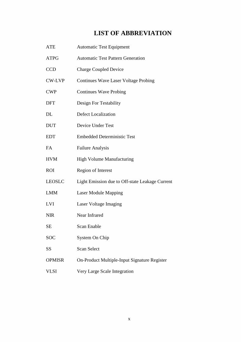
LIST OF ABBREVIATION
ATE Automatic Test Equipment
ATPG Automatic Test Pattern Generation
CCD Charge Coupled Device
CW-LVP Continues Wave Laser Voltage Probing
CWP Continues Wave Probing
DFT Design For Testability
DL Defect Localization
DUT Device Under Test
EDT Embedded Deterministic Test
FA Failure Analysis
HVM High Volume Manufacturing
ROI Region of Interest
LEOSLC Light Emission due to Off-state Leakage Current
LMM Laser Module Mapping
LVI Laser Voltage Imaging
NIR Near Infrared
SE Scan Enable
SOC System On Chip
SS Scan Select
OPMISR On-Product Multiple-Input Signature Register
VLSI Very Large Scale Integration
xi
MODEL HIBRID DIAGNOSIS UNTUK MENGENALPASTI
PUNCA SESARAN RANTAIAN ‘SCAN’ KE ATAS PROSES
FABRIKASI 22nm
ABSTRAK
Dengan perkembangan pesat “Penyatupaduan Skala Sangat Besar” (VLSI),
timbulnya permintaan yang tinggi untuk “Reka Bentuk Boleh Diuji” (DFT). Kajian
luas telah membuktikan bahawa ujian berasaskan ‘Scan’ dapat mencapai liputan
ujian yang baik dengan kos perlaksanan yang rendah, meliputi kawasan ‘die’ yang
kecil dan digunakan secara meluas dalam industri. Model diagnosis untuk mengenal
pasti sesaran dalam rantaian ‘Scan’ memainkan peranan yang penting oleh kerana
10% hinga 30% kecacatan dalam reka bentuk berasaskan ‘Scan’ berlaku di rantaian
‘Scan’ tersebut sendiri. Pada masa ini, terdapat tiga jenis model diagnosis iaitu:
diagnosis berasaskan perisian, penguji dan perkakasan, yang mempunyai beberapa
kelemahan dan batasan. Dalam projek ini, penulis mencadangkan suatu model
analisis hibrid untuk sesaran rantaian ‘Scan’ dengan mengunakan diagnosis
berasaskan perisian untuk mendapatkan senarai suspek sel-sel ‘Scan’ diikuti
diagnosis berasaskan penguji bagi mengasingkan sesaran kepada satu suspek
tunggal. Algoritma diagnosis hibrid yang dicadangkan akan memastikan sesaran
dalam rantaian ‘Scan’ seperti “Stuck-at” dan ‘transition’ dapat diselesaikan dengan
lebih pantas dan kurang kerumitan bagi sesaran yang menyeluruh dan sesaran
sebahagian. Empat kes kajian telah berjaya dilaksanakan untuk menilai algoritma
diagnosis hibrid yang dicadangkan ke atas ‘DUT’ yang berasaskan process fabrikasi
22nm, produk Sistem Atas Cip (SOC), di mana suspek tungal dikenal pasti dalam

xii
proses mengasingkan sesaran dalam kesemua kes kajian serta menunjukan 100%
kadar kejayaan penagasingan sesaran.
xiii
HYBRID DIAGNOSIS MODEL TO DETERMINE FAULT
ISOLATION FOR SCAN CHAIN FAILURE ANALYSIS ON 22nm
FABRICATION PROCESS
ABSTRACT
With the rapid growth of Very Large Scale Integration (VLSI) in complex
designs, there is high demand for Design for Testability (DFT). Vast study has
proven that Scan based testing is achieving good test coverage with lower cost and
smaller die area and is widely used in the industry. Scan chain fault diagnosis plays
an important role as with the implementation of Scan based testing, it is reported that
10%-30% of defects in a Scan based design occurs within the Scan chain itself.
Currently, there are three main types of stand-alone diagnosis models available,
which are: software-based diagnosis, tester-based diagnosis and hardware-based
diagnosis, where each has its disadvantages and limitations. In this project, the author
proposed a hybrid Scan chain failure analysis technique that uses the proposed
software-based diagnosis to obtain a list of possible failing suspect Scan cells,
followed by the proposed tester-based diagnosis to further isolate the fault to a single
failing device suspect. This proposed hybrid diagnosis algorithm ensures that Scan
chain faults such as stuck-at and transition faults can be root-caused with lesser time
and low complexity for both solid and marginal failures. Four case studies were
successfully carried out to evaluate the proposed hybrid diagnosis algorithm on a
22nm fabrication process technology Device under Test (DUT) System-on-Chip
(SOC) product, where the fault isolation was able to isolate a single failing device
suspect for all four case studies, indicating a 100% fault isolation success rate.
1
Chapter 1
INTRODUCTION
This chapter describes the main focus of the research, which is Scan chain
failure isolation using a hybrid method of software-based diagnosis combined with
Laser Module Mapping (LMM) and Continuous Wave Probing (CWP). The problem
statement, objective, scope of study and thesis organization are also defined in this
chapter.
1.1 Background
In reference to Moore’s law, the number of transistors in an integrated circuit
will double its count approximately every two years (Moore G. E., 1975). This
results in more complex designs which end up with a high need for Design for
Testability (DFT) in the industry. A survey by Huang, Y., et al (2008) has proven
that Scan based testing is achieving good test coverage with lower cost and smaller
die area consumed by Scan elements for implementation, which is very effective in
producing testable VLSI design, according to Wang, L.T., et al (2010). Scan
basically converts a digital sequential circuit into a Scan design which then uses
automatic test pattern generation (ATPG) software to detect manufacturing defect or
design issue on the device under test (DUT) (Wang, L.T., et al, 2010). As Scan based
testing is highly used in the industry, it is crucial to make sure that all defect or
design related issues in the Scan chain DFT are identified and root-caused. The most
important aspect in debugging Scan chain failures is identifying the failure boundary
to be as small as possible for failure analysis (FA) and debug applications. Since the
Scan chain test result will not be enough to isolate the defect location, several
2
debugging approaches can be used, such as software-based diagnosis, tester-based
diagnosis, and hardware-based diagnosis.
1.2 Problem Statement
With the increased complexity of DFT implementation and the complex
failure mechanism on 22nm technology, it is becoming very challenging to perform
fault isolation on Scan chain failures using the three available diagnosis approach
mentioned.
The first disadvantage in software-based diagnosis approach is its inability to
isolate precisely to the faulty Scan cell by only depending on High Volume
Manufacturing (HVM) Scan patterns. Secondly, some of the DFT paths are masked
out for manufacturing test optimization as it does not impact the actual device
functionality where coverage loss due to this will result in larger number of suspects
from the diagnosis result. The high number of suspects reported will result in larger
fault isolation area, hence increasing the complexity of defect localization.
The main drawback of tester-based diagnosis on CWP and LMM will be the
time taken to perform binary search to isolate the faulty Scan cell. Moreover,
because this process is performed on a thinned surface DUT, the DUT would not
withstand long hours of probing even with thermal solution applied.
Lastly, it is clearly not practical to implement hardware-based diagnosis as its
implementation cost in the design phase is very high as it requires additional circuit
design to be implemented.
To overcome the limitations faced by the above mentioned diagnosis methods
on Scan chain failures, the author would like to propose an enhanced hybrid Scan
chain failure analysis method using software-based diagnosis combined with LMM
3
and CWP which is part of tester-based diagnosis. Software-based diagnosis on an
Embedded Deterministic Test (EDT) compressed HVM Scan chain pattern and the
original EDT compressed ATPG Scan capture pattern used in HVM will be done to
obtain a list of possible failing suspect Scan cells. This will be followed with LMM
and CWP analysis to further isolate to a single failing device suspect.
1.3 Research Objectives
There are two main objectives in performing this research which are:
i. To achieve a high success rate in performing fault isolation on Scan Chain
failures covering two types of fault models such as stuck-at and transition
failure types on both solid and marginal failing conditions.
ii. To optimize fault isolation on Scan chain failures in terms of time and
complexity.
1.4 Research Methodology
There are three major steps taken to achieve the objective of this research,
which are:
i. To improve fault isolation to a single device suspect for Scan chain failures
using the proposed hybrid diagnosis fault isolation model.
ii. To eliminate the dependency on specially modified ATPG Scan capture
pattern in software-based diagnosis and to be able to minimize the time-
consuming probing (LMM/CWP) experiments which are used in tester-based
diagnosis to root-cause Scan chain failures.
iii. To evaluate the success rate of the proposed hybrid diagnosis fault isolation
algorithm on both solid and marginal Scan chain failures on 22nm fab
process DUT.
4
1.5 Research Scope
This study focuses on the development to enable a hybrid flow using
software-based diagnosis combined with LMM and CWP analysis, where it covers
the following items:
i. Scan chain failure analysis which covers all Scan chain failure fault types
except for Slow/Fast fault on 22nm technology flip-chip DUT.
ii. Marginal and solid Scan chain failure behavior will be evaluated on the
proposed isolation methodology.
iii. The study will only focus on fault isolation of a single falling fault on a
particular Scan chain.
1.6 Research Contribution
The main contribution of this research is to reduce the complexity and time
taken for Scan chain failure diagnosis from an FA perspective where it becomes
more practical for industrial application to focus on large number of failures. One
such condition is diagnosis on DUT failing from wafer sort, where a large number of
DUT on the same wafer or lot may fail Scan chain test.
1.7 Thesis Structure
This dissertation will be divided into five chapters. In Chapter 1, which is the
introduction of the dissertation, the background of the research, problem statement,
proposed solution, objective and scope of study as well as dissertation organization
will be outlined.
Chapter 2 which will be the literature review, will discuss on the present
diagnosis methods’ pros and cons and also cover their experimental components.
Other relevant information regarding the research such as the test pattern algorithm,
5
concept of CWP and LMM and the fault isolation validation theory will also be
discussed in this chapter.
Chapter 3 explains the methodology of the proposed hybrid Scan chain
diagnosis flow to narrow down to a single faulty node for stuck-at and transition
Scan chain failures fault types and result verification flow during data collection.
Chapter 4 of the dissertation will discuss the result and discussion on the
outcome of the proposed hybrid diagnosis model on Scan chain debug for four
different test case conditions: (a) fault isolation on Scan chain solid stuck-at failure,
(b) fault isolation on Scan chain solid transition failure, (c) fault isolation on Scan
chain marginal stuck-at failure, and (d) fault isolation on Scan chain marginal
transition failure.
Chapter 5 is the final chapter of the dissertation which concentrates on the
research conclusion and areas of improvement of this research.
6
Chapter 2
LITERATURE RIVIEW
The literature review was conducted upfront focusing on the present
diagnosis methods’ pros and cons as well as their experimental components. Other
relevant information regarding the research such as Scan Chain fault mode types, the
pattern generation algorithm, concept of CWP or also known as Continues Wave
Laser Voltage Probe (CW-LVP) and LMM or also known as Laser Voltage Imaging
(LVI) and the fault isolation validation theory will also be discussed in this chapter.
2.1 Fault Models
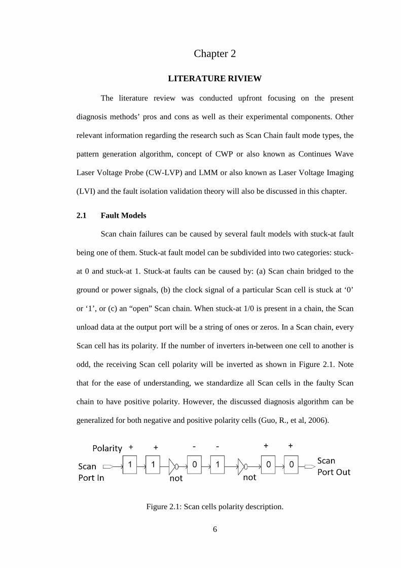
Scan chain failures can be caused by several fault models with stuck-at fault
being one of them. Stuck-at fault model can be subdivided into two categories: stuck-
at 0 and stuck-at 1. Stuck-at faults can be caused by: (a) Scan chain bridged to the
ground or power signals, (b) the clock signal of a particular Scan cell is stuck at ‘0’
or ‘1’, or (c) an “open” Scan chain. When stuck-at 1/0 is present in a chain, the Scan
unload data at the output port will be a string of ones or zeros. In a Scan chain, every
Scan cell has its polarity. If the number of inverters in-between one cell to another is
odd, the receiving Scan cell polarity will be inverted as shown in Figure 2.1. Note
that for the ease of understanding, we standardize all Scan cells in the faulty Scan
chain to have positive polarity. However, the discussed diagnosis algorithm can be
generalized for both negative and positive polarity cells (Guo, R., et al, 2006).
Figure 2.1: Scan cells polarity description.
7
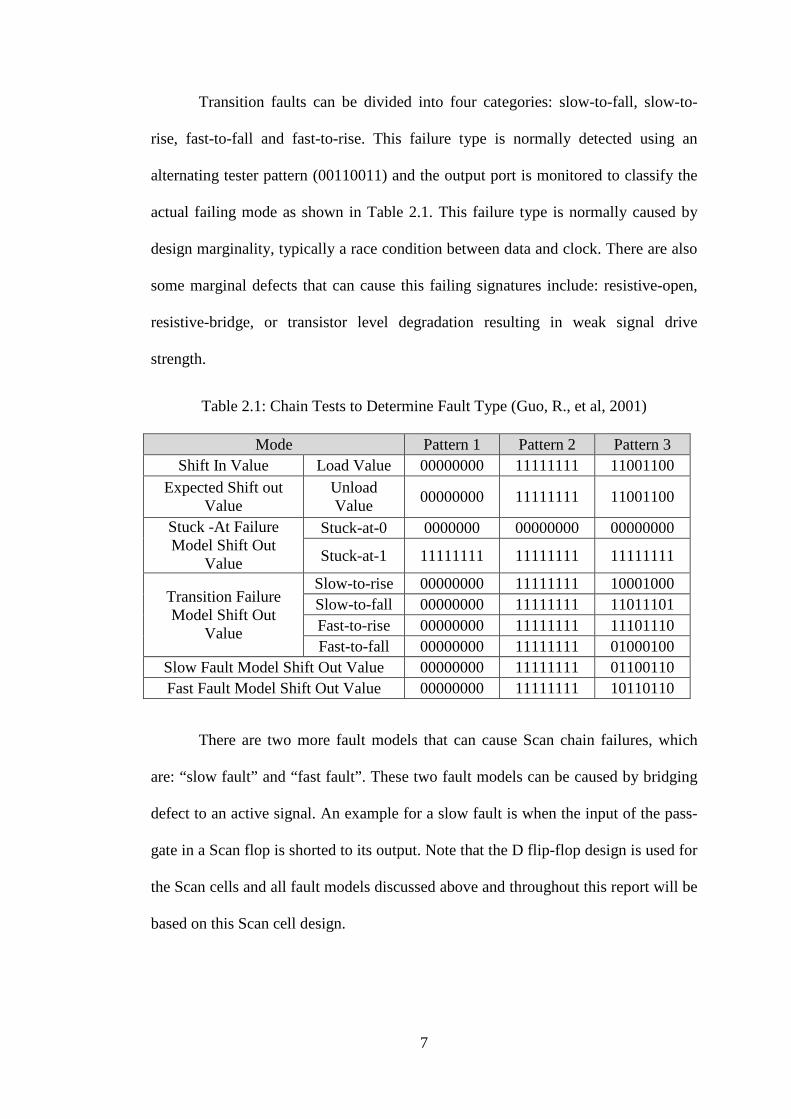
Transition faults can be divided into four categories: slow-to-fall, slow-to-
rise, fast-to-fall and fast-to-rise. This failure type is normally detected using an
alternating tester pattern (00110011) and the output port is monitored to classify the
actual failing mode as shown in Table 2.1. This failure type is normally caused by
design marginality, typically a race condition between data and clock. There are also
some marginal defects that can cause this failing signatures include: resistive-open,
resistive-bridge, or transistor level degradation resulting in weak signal drive
strength.
Table 2.1: Chain Tests to Determine Fault Type (Guo, R., et al, 2001)
Mode Pattern 1 Pattern 2 Pattern 3 Shift In Value Load Value 00000000 11111111 11001100
Expected Shift out Value
Unload Value 00000000 11111111 11001100
Stuck -At Failure Model Shift Out
Value
Stuck-at-0 0000000 00000000 00000000
Stuck-at-1 11111111 11111111 11111111
Transition Failure Model Shift Out
Value
Slow-to-rise 00000000 11111111 10001000 Slow-to-fall 00000000 11111111 11011101 Fast-to-rise 00000000 11111111 11101110 Fast-to-fall 00000000 11111111 01000100
Slow Fault Model Shift Out Value 00000000 11111111 01100110 Fast Fault Model Shift Out Value 00000000 11111111 10110110
There are two more fault models that can cause Scan chain failures, which
are: “slow fault” and “fast fault”. These two fault models can be caused by bridging
defect to an active signal. An example for a slow fault is when the input of the pass-
gate in a Scan flop is shorted to its output. Note that the D flip-flop design is used for
the Scan cells and all fault models discussed above and throughout this report will be
based on this Scan cell design.
8
2.2 Scan Chain Diagnosis
Along the years, a lot of work has been done to improve Scan chain fault
isolation using three main diagnosis methods: software-based diagnosis, tester-based
diagnosis, and hardware-based diagnosis.
Software-Based Diagnosis 2.2.1
Software-based diagnosis mainly uses the concept of comparing the expected
output (simulation data) with the actual shift-out data from the DUT for a given
tester pattern to determine the type of failure as well as the failing boundary. Two
forms of test patterns typically used are Scan chain pattern and ATPG Scan capture
pattern.
Scan chain pattern is normally used to determine the faulty chain and the fault
type in the faulty chain using chain test (Scan mode test). This applies to both
compressed and non-compressed patterns. In a non-compressed pattern architecture,
each Scan chain has its own input/output port, and the failing chain can be
determined by comparing the output port data with the simulated or expected output.
Figure 2.2 shows a design with three Scan chains where the first Scan chain has a
stuck-at 1 failure and the third Scan chain has a stuck-at 0 failure.
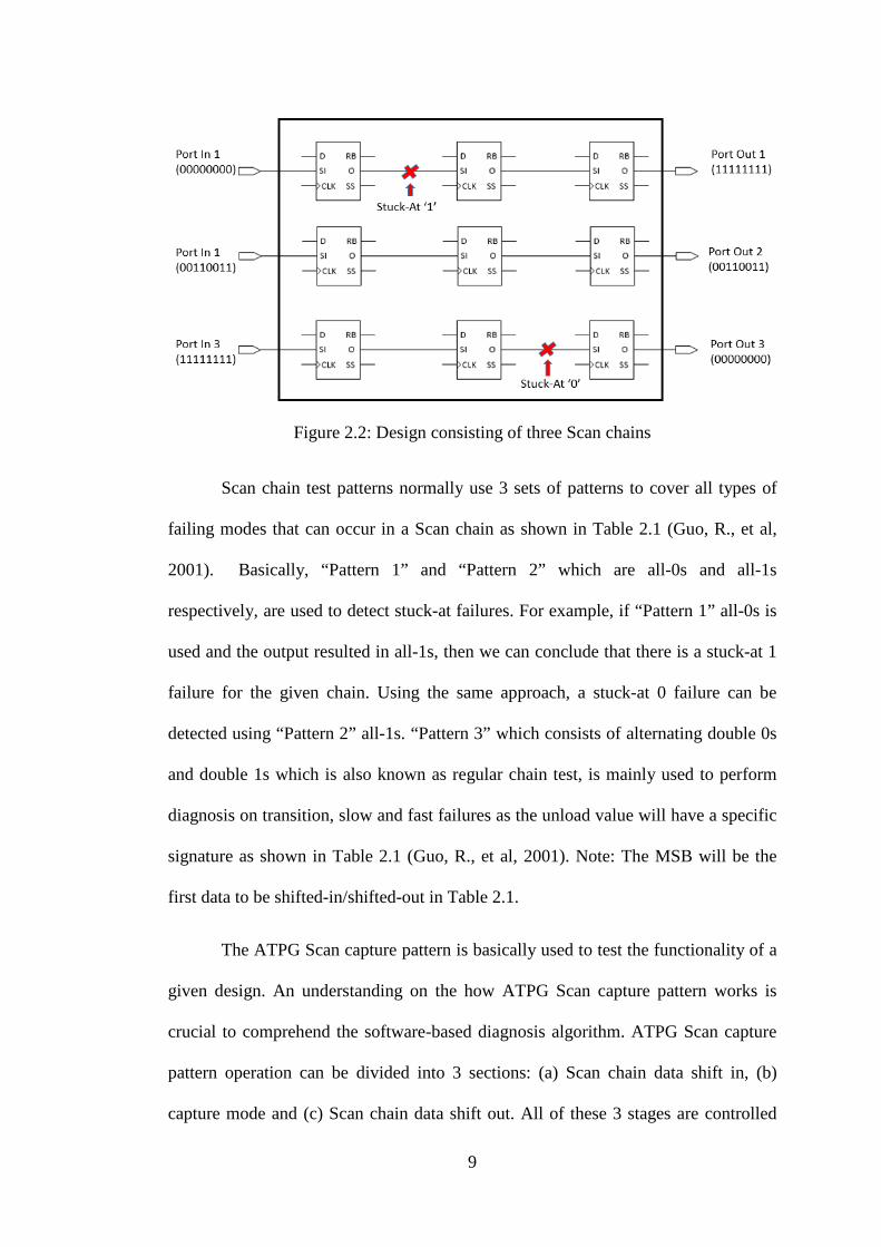
9
Figure 2.2: Design consisting of three Scan chains
Scan chain test patterns normally use 3 sets of patterns to cover all types of
failing modes that can occur in a Scan chain as shown in Table 2.1 (Guo, R., et al,
2001). Basically, “Pattern 1” and “Pattern 2” which are all-0s and all-1s
respectively, are used to detect stuck-at failures. For example, if “Pattern 1” all-0s is
used and the output resulted in all-1s, then we can conclude that there is a stuck-at 1
failure for the given chain. Using the same approach, a stuck-at 0 failure can be
detected using “Pattern 2” all-1s. “Pattern 3” which consists of alternating double 0s
and double 1s which is also known as regular chain test, is mainly used to perform
diagnosis on transition, slow and fast failures as the unload value will have a specific
signature as shown in Table 2.1 (Guo, R., et al, 2001). Note: The MSB will be the
first data to be shifted-in/shifted-out in Table 2.1.
The ATPG Scan capture pattern is basically used to test the functionality of a
given design. An understanding on the how ATPG Scan capture pattern works is
crucial to comprehend the software-based diagnosis algorithm. ATPG Scan capture
pattern operation can be divided into 3 sections: (a) Scan chain data shift in, (b)
capture mode and (c) Scan chain data shift out. All of these 3 stages are controlled
10
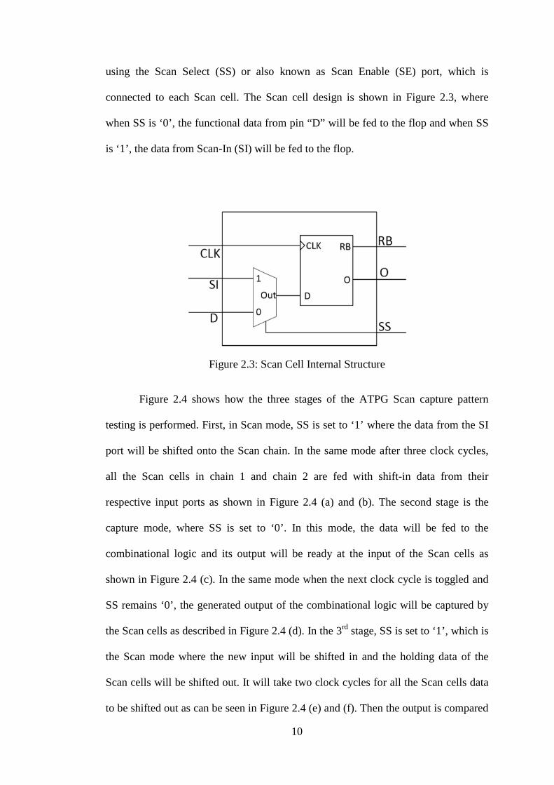
using the Scan Select (SS) or also known as Scan Enable (SE) port, which is
connected to each Scan cell. The Scan cell design is shown in Figure 2.3, where
when SS is ‘0’, the functional data from pin “D” will be fed to the flop and when SS
is ‘1’, the data from Scan-In (SI) will be fed to the flop.
Figure 2.3: Scan Cell Internal Structure
Figure 2.4 shows how the three stages of the ATPG Scan capture pattern
testing is performed. First, in Scan mode, SS is set to ‘1’ where the data from the SI
port will be shifted onto the Scan chain. In the same mode after three clock cycles,
all the Scan cells in chain 1 and chain 2 are fed with shift-in data from their
respective input ports as shown in Figure 2.4 (a) and (b). The second stage is the
capture mode, where SS is set to ‘0’. In this mode, the data will be fed to the
combinational logic and its output will be ready at the input of the Scan cells as
shown in Figure 2.4 (c). In the same mode when the next clock cycle is toggled and
SS remains ‘0’, the generated output of the combinational logic will be captured by
the Scan cells as described in Figure 2.4 (d). In the 3rd stage, SS is set to ‘1’, which is
the Scan mode where the new input will be shifted in and the holding data of the
Scan cells will be shifted out. It will take two clock cycles for all the Scan cells data
to be shifted out as can be seen in Figure 2.4 (e) and (f). Then the output is compared
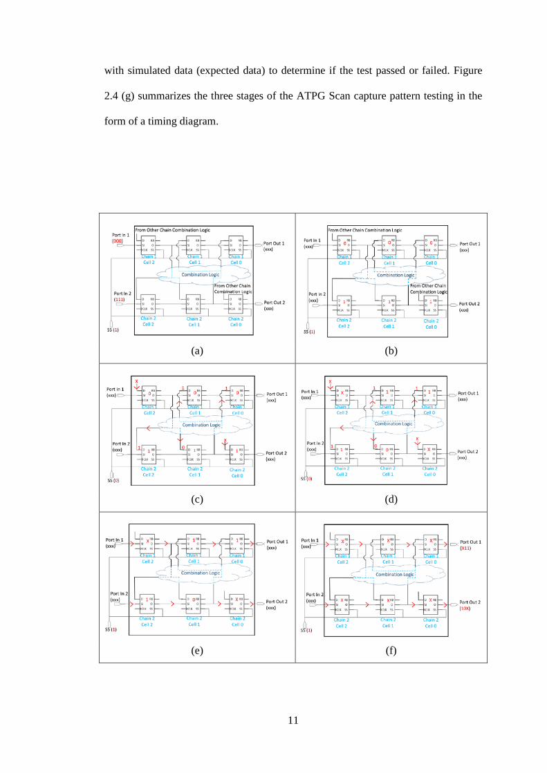
11
with simulated data (expected data) to determine if the test passed or failed. Figure
2.4 (g) summarizes the three stages of the ATPG Scan capture pattern testing in the
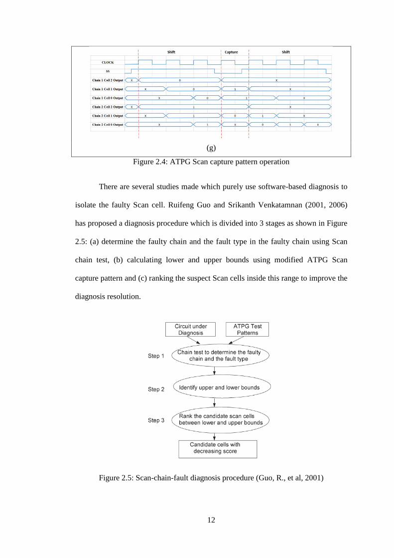
form of a timing diagram.
(a) (b)
(c) (d)
(e) (f)
12
(g)
Figure 2.4: ATPG Scan capture pattern operation
There are several studies made which purely use software-based diagnosis to
isolate the faulty Scan cell. Ruifeng Guo and Srikanth Venkatamnan (2001, 2006)
has proposed a diagnosis procedure which is divided into 3 stages as shown in Figure
2.5: (a) determine the faulty chain and the fault type in the faulty chain using Scan
chain test, (b) calculating lower and upper bounds using modified ATPG Scan
capture pattern and (c) ranking the suspect Scan cells inside this range to improve the
diagnosis resolution.
Figure 2.5: Scan-chain-fault diagnosis procedure (Guo, R., et al, 2001)
13
As for the first step (a), the same method is used as discussed above, where 3
types of Scan Chain patterns are used and with reference to Table 2.1, the faulty Scan
chain and the fault type is determined.
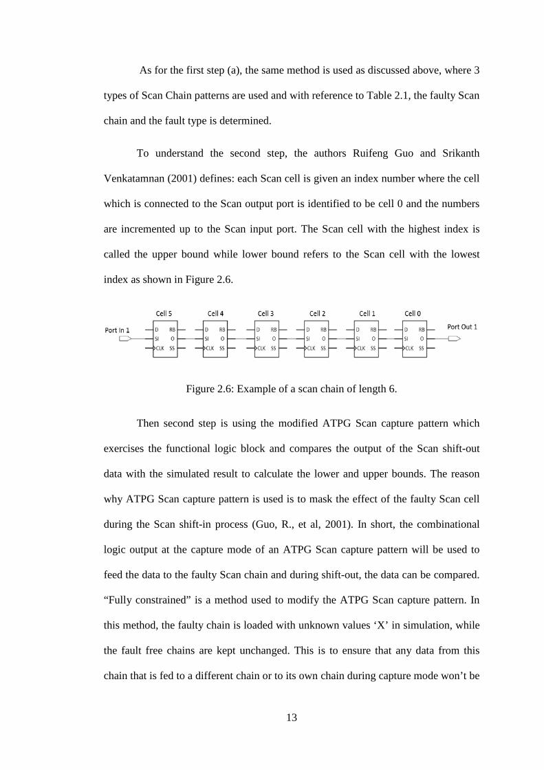
To understand the second step, the authors Ruifeng Guo and Srikanth
Venkatamnan (2001) defines: each Scan cell is given an index number where the cell
which is connected to the Scan output port is identified to be cell 0 and the numbers
are incremented up to the Scan input port. The Scan cell with the highest index is
called the upper bound while lower bound refers to the Scan cell with the lowest
index as shown in Figure 2.6.
Figure 2.6: Example of a scan chain of length 6.
Then second step is using the modified ATPG Scan capture pattern which
exercises the functional logic block and compares the output of the Scan shift-out
data with the simulated result to calculate the lower and upper bounds. The reason
why ATPG Scan capture pattern is used is to mask the effect of the faulty Scan cell
during the Scan shift-in process (Guo, R., et al, 2001). In short, the combinational
logic output at the capture mode of an ATPG Scan capture pattern will be used to
feed the data to the faulty Scan chain and during shift-out, the data can be compared.
“Fully constrained” is a method used to modify the ATPG Scan capture pattern. In
this method, the faulty chain is loaded with unknown values ‘X’ in simulation, while
the fault free chains are kept unchanged. This is to ensure that any data from this
chain that is fed to a different chain or to its own chain during capture mode won’t be
14
used for result comparison during the shift-out, where the bit will be masked. There
are several other modifications during logic simulation that needs to be in place to
calculate the upper and lower bounds and this is also dependent on the failure mode.
Suppose the fault type is stuck-at 1 and “Scan cell 1” of the faulty chain is
defined to hold a value ‘0’ based on the logic simulation of the modified ATPG Scan
capture pattern. When this modified pattern is loaded on the tester and the observed
value of Scan cell 1 is ‘0’, then it can be concluded that the stuck-at 1 fault lies in the
upstream cells of Scan cell 1. On the other hand, if the observed value from tester for
Scan cell 1 is ‘1’, then it can be concluded that the stuck-at 1 fault lies in the
downstream cells of Scan cell 1. Example on how a stuck-at 1 failure’s upper and
lower bounds can be detected in a faulty chain of 6 Scan cells is shown in Figure 2.7
(Guo, R., et al, 2006).
Figure 2.7: Determining the upper/lower bounds for a Stuck-at 1 Failure
For transition faults, two adjacent cells’ values are monitored to determine
the upper and lower bounds. For example, for a fast-to-fall transition failure, Scan
cells 2 and 3 are evaluated. Based on the logic simulation of the modified ATPG
Scan capture pattern, Scan cell 2 and Scan cell 3 are assigned to hold the same value
of ‘1’. If the observed faulty chain shows that Scan cell 2 and Scan cell 3 are
holding the same value as in simulation, then the failure will be on the upstream of
15
Scan cell 2. On the other hand, if the observed value of Scan cell 2 is ‘0’ and Scan
cell 3 is ‘1’, then the fault must be in the downstream cells of Scan cell 2. Example
on how a fast-to-fall transition failure’s upper and lower bounds can be detected in a
faulty chain of 6 Scan cells is shown in Figure 2.8.
Figure 2.8: Determining the upper/lower bounds for a Fast-to-fall transition Failure
To determine “fast/slow” fault bounds, values for two adjacent cells are
observed, similar to a transition failure. In the logic simulation of the modified
ATPG Scan capture pattern, the adjacent Scan cell must be assigned with different
binary values. Example on how a “fast” failure’s upper and lower bounds can be
detected in a faulty chain of 6 Scan cells is shown in Figure 2.9. In this example, the
values of Scan cells 4 and 3 are used to determine the upper bound and the values of
Scan cells 2 and 1 is used to determine the lower bound.
Figure 2.9: Determining the upper/lower bounds for a fast fault type Failure
16
The 3rd step for this software-based diagnosis is to score and rank the suspect
obtained based on the lower and upper bounds. In this step, a specific set of logic
modified ATPG Scan capture patterns is simulated for each Scan cell suspect in the
lower and upper bound range. The DUT is re-tested again with these patterns and the
observed faulty circuit output is compared against the simulated outputs. In reference
to a matching algorithm, a score is computed and assigned to each suspected Scan
cell. The higher the score, the higher the probability that the suspect could be the
actual defect location. The scoring is mainly computed based on the metrics of
intersections, mispredictions and nonpredictions as shown in Figure 2.10 (Guo, R., et
al, 2006; Venkataraman, S., et al, 2000).
Figure 2.10: Metrics to calculate scores (Venkataraman, S., et al, 2000)
A failure that is predicted in simulation and also observed in tester is
categorized as intersection. A failure which is predicted by logic simulation but not
observed on tester is categorized as misprediction. On the other hand, a failure not
predicted by simulation but was observed failing on tester is called nonprediction.
Within these three categories, intersection and nonprediction are the primary
components used for score calculation in comparison to misprediction. On top of it, a
second set of metric known as vectorwise intersection is also considered during the
score calculation. A vectorwise intersection is a count of test pattern where the tester
17
observed output for a test pattern is exactly the same as compared to the simulation
result. The score calculation for each suspect consists of the accumulated values for
vectorwise intersections, intersections, nonpredictions and mispredictions for all the
ATPG Scan capture patterns whereby vectorwise intersection is found to be the
strongest metric and misprediction as the weakest metric (Guo, R., et al, 2006;
Venkataraman, S., et al, 2000).
With these three main steps of software-based diagnosis, the fault type,
failing chain information and suspect Scan cell list with scoring and ranking can be
obtained. However, this proposed methodology is not practical for large designs as
the number of test data volume far exceeds the capacities of the Automatic Test
Equipment (ATE). To overcome this, Yu Juang, Wu-Tung Cheng and Janusz Rajski
(2005) introduced diagnosis for Scan chain failures using compressed pattern, which
was used to contain test costs while achieving the required test quality levels but still
adopting the general diagnosis flow, where a modified ATPG Scan capture pattern
which is specific to each failing DUT is required to obtain accurate diagnosis
isolation of the faulty Scan cell. Embedded Deterministic Test (EDT) compression
technique is widely adopted in the industry. Two complementary aspects are
involved in this compression technique: hardware that is incorporated on chip and
the software (ATPG) that uses the on-chip hardware to generate highly compressed
tests which reduce the test data volume and test application time (Huang, Y., et al,
2005). For EDT compression to be enabled, hardware blocks called decompressor
and compactor are integrated into the circuit design. Decompressor transforms the
data supplied on the Scan input port and feeds a large number of internal Scan chains
(Huang, Y., et al, 2005). Compactor, on the other hand, takes in a large number of
internal Scan chains into a data stream that is delivered on Scan output channels for
18
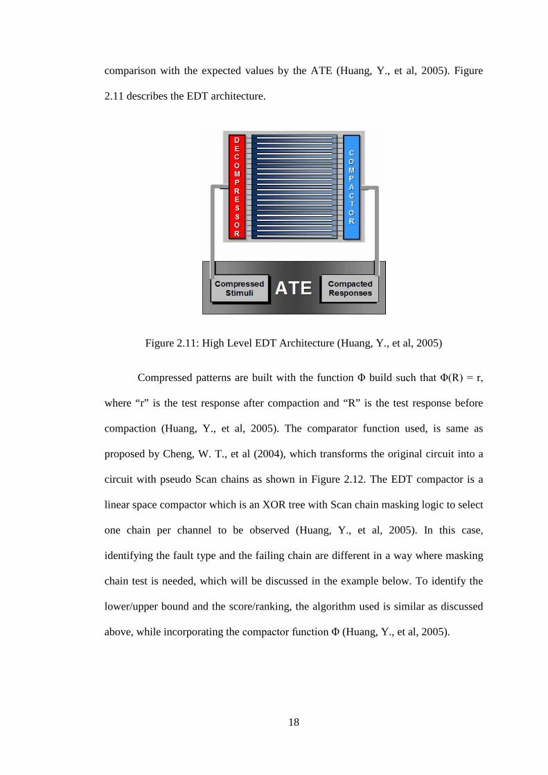
comparison with the expected values by the ATE (Huang, Y., et al, 2005). Figure
2.11 describes the EDT architecture.
Figure 2.11: High Level EDT Architecture (Huang, Y., et al, 2005)
Compressed patterns are built with the function Φ build such that Φ(R) = r,
where “r” is the test response after compaction and “R” is the test response before
compaction (Huang, Y., et al, 2005). The comparator function used, is same as
proposed by Cheng, W. T., et al (2004), which transforms the original circuit into a
circuit with pseudo Scan chains as shown in Figure 2.12. The EDT compactor is a
linear space compactor which is an XOR tree with Scan chain masking logic to select
one chain per channel to be observed (Huang, Y., et al, 2005). In this case,
identifying the fault type and the failing chain are different in a way where masking
chain test is needed, which will be discussed in the example below. To identify the
lower/upper bound and the score/ranking, the algorithm used is similar as discussed
above, while incorporating the compactor function Φ (Huang, Y., et al, 2005).
19
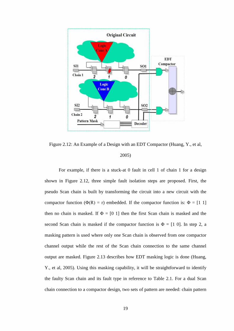
Figure 2.12: An Example of a Design with an EDT Compactor (Huang, Y., et al,
2005)
For example, if there is a stuck-at 0 fault in cell 1 of chain 1 for a design
shown in Figure 2.12, three simple fault isolation steps are proposed. First, the
pseudo Scan chain is built by transforming the circuit into a new circuit with the
compactor function (Φ(R) = r) embedded. If the compactor function is: Φ = [1 1]
then no chain is masked. If Φ = [0 1] then the first Scan chain is masked and the
second Scan chain is masked if the compactor function is Φ = [1 0]. In step 2, a
masking pattern is used where only one Scan chain is observed from one compactor
channel output while the rest of the Scan chain connection to the same channel
output are masked. Figure 2.13 describes how EDT masking logic is done (Huang,
Y., et al, 2005). Using this masking capability, it will be straightforward to identify
the faulty Scan chain and its fault type in reference to Table 2.1. For a dual Scan
chain connection to a compactor design, two sets of pattern are needed: chain pattern
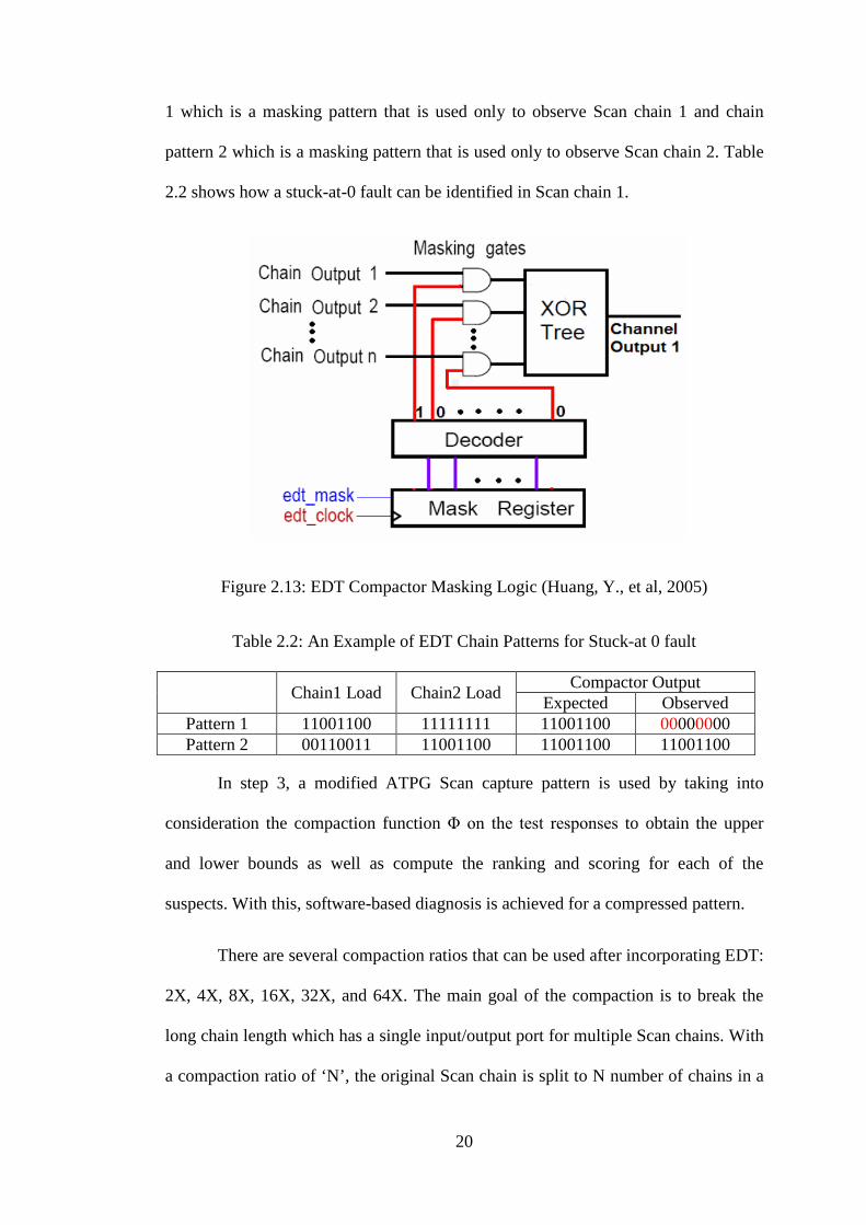
20
1 which is a masking pattern that is used only to observe Scan chain 1 and chain
pattern 2 which is a masking pattern that is used only to observe Scan chain 2. Table
2.2 shows how a stuck-at-0 fault can be identified in Scan chain 1.
Figure 2.13: EDT Compactor Masking Logic (Huang, Y., et al, 2005)
Table 2.2: An Example of EDT Chain Patterns for Stuck-at 0 fault
Chain1 Load Chain2 Load Compactor Output Expected Observed
Pattern 1 11001100 11111111 11001100 00000000 Pattern 2 00110011 11001100 11001100 11001100
In step 3, a modified ATPG Scan capture pattern is used by taking into
consideration the compaction function Φ on the test responses to obtain the upper
and lower bounds as well as compute the ranking and scoring for each of the
suspects. With this, software-based diagnosis is achieved for a compressed pattern.
There are several compaction ratios that can be used after incorporating EDT:
2X, 4X, 8X, 16X, 32X, and 64X. The main goal of the compaction is to break the
long chain length which has a single input/output port for multiple Scan chains. With
a compaction ratio of ‘N’, the original Scan chain is split to N number of chains in a
21
balanced manner where the split Scan chains’ length is close to 1/N of the original
Scan chain length. For example, if 2X compaction ratio is used for an original Scan
chain length of 20 Scan cells, then with EDT compaction it will split it to 2 chains
with 10 Scan cells per split chain. With this, diagnosis accuracy can be improved as
the number of suspects list is reduced in the first step of the Scan chain diagnosis,
with the faulty chain and fault mode identified.
In short, software-based diagnosis on a compressed pattern is widely used in
the industry compared to hardware-based as it does not require design modification.
It has a dependency on modified ATPG Scan capture patterns that need to be
generated for a failing DUT for accurate diagnosis result compared to diagnosis
result obtained from the original ATPG Scan capture pattern used in High Volume
Manufacturing (HVM).
Tester-based Diagnosis 2.2.2
Tester based Diagnosis is basically using a tester pattern which is similar to
Scan chain pattern used in software based diagnosis: alternating shift-in data
(0011/0101) or a constant shift-in data (0000/1111) into the Scan chain and using a
defect localization (DL) equipment to observe abnormal responses at the region of
interest (ROI) by adopting a binary search method to isolate the failing Scan cells.
There are several DL techniques such as Electron-beam (E-beam) probing (De, K., et
al, 1995), Light Emission due to Off-State Leakage Current Probing (LEOSLC)
(Song, P., et al, 2004), CWP (Kasapi, S., et al, 2011) and LMM (Kasapi, S., et al,
2011; Liao, J. Y., et al, 2010) which are used to perform hardware-based diagnosis.
Voltage-contrast imaging is the key principle used in E-beam probing. A
secondary electron is generated and can be detected when the E-beam is in contact
with the surface of the device. The detection mechanism produces a real-time image
22
of the surface of the device on a computer monitor (Lindberg, G., et al, 1994).
Location of the device which is in state zero or low voltage appear to be lighter since
more secondary electrons are generated. On the other hand, device with state one or
high voltage appear darker since it emits lesser secondary electrons. An additional
feature to this is to perform waveform probing at a particular point on the surface of
the device, similar to that of a sampling oscilloscope (Lindberg, G., et al, 1994). E-
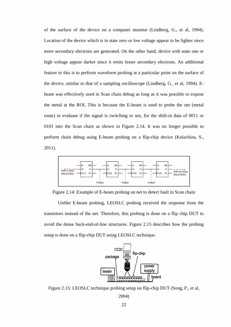
beam was effectively used in Scan chain debug as long as it was possible to expose
the metal at the ROI. This is because the E-beam is used to probe the net (metal
route) to evaluate if the signal is switching or not, for the shift-in data of 0011 or
0101 into the Scan chain as shown in Figure 2.14. It was no longer possible to
perform chain debug using E-beam probing on a flip-chip device (Kolachina, S.,
2011).
Figure 2.14: Example of E-beam probing on net to detect fault in Scan chain
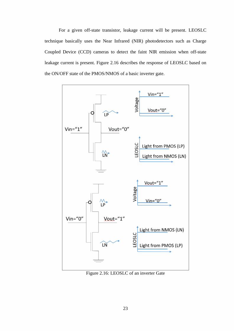
Unlike E-beam probing, LEOSLC probing received the response from the
transistors instead of the net. Therefore, this probing is done on a flip chip DUT to
avoid the dense back-end-of-line structures. Figure 2.15 describes how the probing
setup is done on a flip-chip DUT using LEOSLC technique.
Figure 2.15: LEOSLC technique probing setup on flip-chip DUT (Song, P., et al,
2004)
23
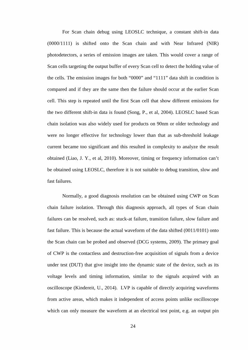
For a given off-state transistor, leakage current will be present. LEOSLC
technique basically uses the Near Infrared (NIR) photodetectors such as Charge
Coupled Device (CCD) cameras to detect the faint NIR emission when off-state
leakage current is present. Figure 2.16 describes the response of LEOSLC based on
the ON/OFF state of the PMOS/NMOS of a basic inverter gate.
Figure 2.16: LEOSLC of an inverter Gate
24
For Scan chain debug using LEOSLC technique, a constant shift-in data
(0000/1111) is shifted onto the Scan chain and with Near Infrared (NIR)
photodetectors, a series of emission images are taken. This would cover a range of
Scan cells targeting the output buffer of every Scan cell to detect the holding value of
the cells. The emission images for both “0000” and “1111” data shift in condition is
compared and if they are the same then the failure should occur at the earlier Scan
cell. This step is repeated until the first Scan cell that show different emissions for
the two different shift-in data is found (Song, P., et al, 2004). LEOSLC based Scan
chain isolation was also widely used for products on 90nm or older technology and
were no longer effective for technology lower than that as sub-threshold leakage
current became too significant and this resulted in complexity to analyze the result
obtained (Liao, J. Y., et al, 2010). Moreover, timing or frequency information can’t
be obtained using LEOSLC, therefore it is not suitable to debug transition, slow and
fast failures.
Normally, a good diagnosis resolution can be obtained using CWP on Scan
chain failure isolation. Through this diagnosis approach, all types of Scan chain
failures can be resolved, such as: stuck-at failure, transition failure, slow failure and
fast failure. This is because the actual waveform of the data shifted (0011/0101) onto
the Scan chain can be probed and observed (DCG systems, 2009). The primary goal
of CWP is the contactless and destruction-free acquisition of signals from a device
under test (DUT) that give insight into the dynamic state of the device, such as its
voltage levels and timing information, similar to the signals acquired with an
oscilloscope (Kindereit, U., 2014). LVP is capable of directly acquiring waveforms
from active areas, which makes it independent of access points unlike oscilloscope
which can only measure the waveform at an electrical test point, e.g. an output pin