Embed Size (px)
Citation preview
Hydride Vapor Phase Epitaxy of GaN on SiliconCovered by Nanostructures
U Jahn1, M Musolino1, J Lahnemann1, P Dogan1, S FernandezGarrido1, J F Wang2, K Xu2, D Cai2, L F Bian2, X J Gong2 and HYang2
1 Paul-Drude-Institut fur Festkorperelektronik, Hausvogteiplatz 5-7, 10117 Berlin,Germany2 Suzhou Institute of Nano-tech and Nano-bionics, Chinese Academy of Sciences,398 Roushui Road, Suzhou City, 215123 P. R. China
Abstract. Several ten µm GaN have been deposited on a silicon substrate usinga two-step hydride vapor phase epitaxy (HVPE) process. The substrates havebeen covered by AlN layers and GaN nanostructures grown by plasma-assistedmolecular-beam epitaxy. During the first low-temperature (low-T) HVPE step,stacking faults (SF) form, which show distinct luminescence lines and stripe-likefeatures in cathodoluminescence images of the cross-section of the layers. Thesecathodoluminescence features allow for an insight into the growth process. Duringa second high-temperature (high-T) step, the SFs disappear, and the luminescence ofthis part of the GaN layer is dominated by the donor-bound exciton. For templatesconsisting of both a thin AlN buffer and GaN nanostructures, a silicon incorporationinto the GaN grown by HVPE is not observed. Moreover, the growth mode of the(high-T) HVPE step depends on the specific structure of the AlN/GaN template,where in a first case, the epitaxy is dominated by the formation of slowly growingfacets, while in a second case, the epitaxy proceeds directly along the c-axis.
For templates without GaN nanostructures, cathodoluminescence spectra excitedclose to the Si/GaN interface show a broadening toward higher energies indicatinga silicon incorporation on a high dopant level.
PACS numbers: 78.30.Fs, 78.20.-e, 78.55.Cr, 78.60.Hk
This is an author-created,un-copyedited version of an article accepted for publication inSemiconductor Science and Technology. IOP Publishing Ltd is not responsible for any errors oromissions in this version of the manuscript or any version derived from it. The Version of Record isavailable online at doi:10.1088/0268-1242/31/6/065018
arX
iv:1
605.
0308
9v1
[co
nd-m
at.m
trl-
sci]
10
May
201
6
GaN on Si by HVPE 2
1. Introduction
In order to improve, e. g., the performance of nitride-based laser diodes, the densityof threading dislocations penetrating into the corresponding layer systems need tobe further reduced. This is a difficult task, when growing such device structures onforeign substrates, e. g., on sapphire, silicon carbide, or silicon due to a strain-relatedgeneration of extended defects. Therefore, the interest in the fabrication of bulk GaNsubstrates as well as of free-standing GaN layers (FS-GaN) for a subsequent homo-epitaxial deposition of device structures is growing. Hydride vapor phase epitaxy(HVPE) has already proven to be well suited for the fabrication of FS-GaN withthreading dislocation densities below 104 cm−2. [1] Commonly, sapphire wafers areused as substrates for the HVPE process to grow FS-GaN. [1, 2, 3]
However, due to the low cost, available large wafer size, and well-establishedchemical etching techniques, silicon is very attractive to serve as a substrate materialfor the growth of FS-GaN. So far, two key problems, which depend on each other,have prevented a successful use of silicon as a substrate for the HVPE growth ofFS-GaN. First, there is a high lattice mismatch (17%) and a large difference in thethermal expansion coefficient (56%) between GaN and silicon giving rise to crackingof the GaN during the growth as well as during the cooling of the GaN substratefrom the growth temperature down to room temperature. Second, silicon is notstable in the reactive ambiance and at the high temperatures applied during theHVPE process, where the reaction between silicon and the chlorine-based growthchemistry often results in a mixture of silicon, Ga, and N including SiNx phases(silicon-melt-back etching) instead of the intended GaN. [4, 5]
AlN buffer layers and a two-step growth mode with first a low-temperature(low-T) step have been used to suppress the silicon-melt-back etching. Alsoselective-area growth (SAG), where the templates for the HVPE consist of a few100 µm large growth windows to prevent cracking, has been applied. [6] However,the optimization of the protecting interlayer is very critical. For too thin AlN bufferlayers, the reaction with silicon hinders an epitaxial growth of GaN. For too thickbuffer layers, micro-cracks can appear during the growth, which again open a wayfor a reaction of Si with Ga or N. Thus, although the growth of a few ten µm thickGaN layers on silicon by HVPE has already been reported about 10 years ago [7, 8],a long-term HVPE growth of GaN on silicon resulting in substrates with a thicknessof several hundred µm is still challenging.
Furthermore, the use of SAG or epitaxial lateral overgrowth techniquesrequire micrometer masking, ex situ SiO2 or SiNx deposition and multi-stepphotolithography, which increase the process complexity and costs. Hersee et al.[9]proposed a nano-heteroepitaxy technique, taking advantage of three-dimensionalstress relief mechanisms, which is expected to result in a further improvement ofGaN epilayers grown on foreign substrates. Based on this method, several authorshave discussed a new non-lithographic nano-heteroepitaxy approach relying on
GaN on Si by HVPE 3
self-assembled nanostructures in order to reduce the process steps and costs.[10, 11, 12, 13, 14] Kwon et al. [14] have used a 50 nm thick sputtered AlN buffer onsilicon, on which they have grown self-assembled nano-needles and -rods during afirst low-T HVPE step at 600 and 650 ◦C, respectively. Subsequently, 0.5–2 µm thickGaN layers have been overgrown in a second HVPE step at 1040 ◦C. The optical near-band gap emission of these GaN layers are red-shifted with regard to the expectedspectral position, the origin of which has not been analyzed in detail. Moreover,longer high-T HVPE runs to obtain thick GaN layers have not been carried out.
In this work, we are reporting on the HVPE growth of thick GaN layers onself-assembled GaN nanostructures, the latter having been deposited on Si(111)substrates with AlN buffer layers using plasma-assisted molecular-beam epitaxy(MBE). The HVPE growth process is investigated by spatially and spectrally resolvedcathodoluminescence (CL) spectroscopy in a scanning electron microscope (SEM) atcross-sections of the layers. By adding GaN nano-structures as nucleation sites andapplying a two-step HVPE growth process, silicon incorporation into several ten µmthick GaN layers could be prevented.
2. Experimental details
2.1. Preparation of the templates
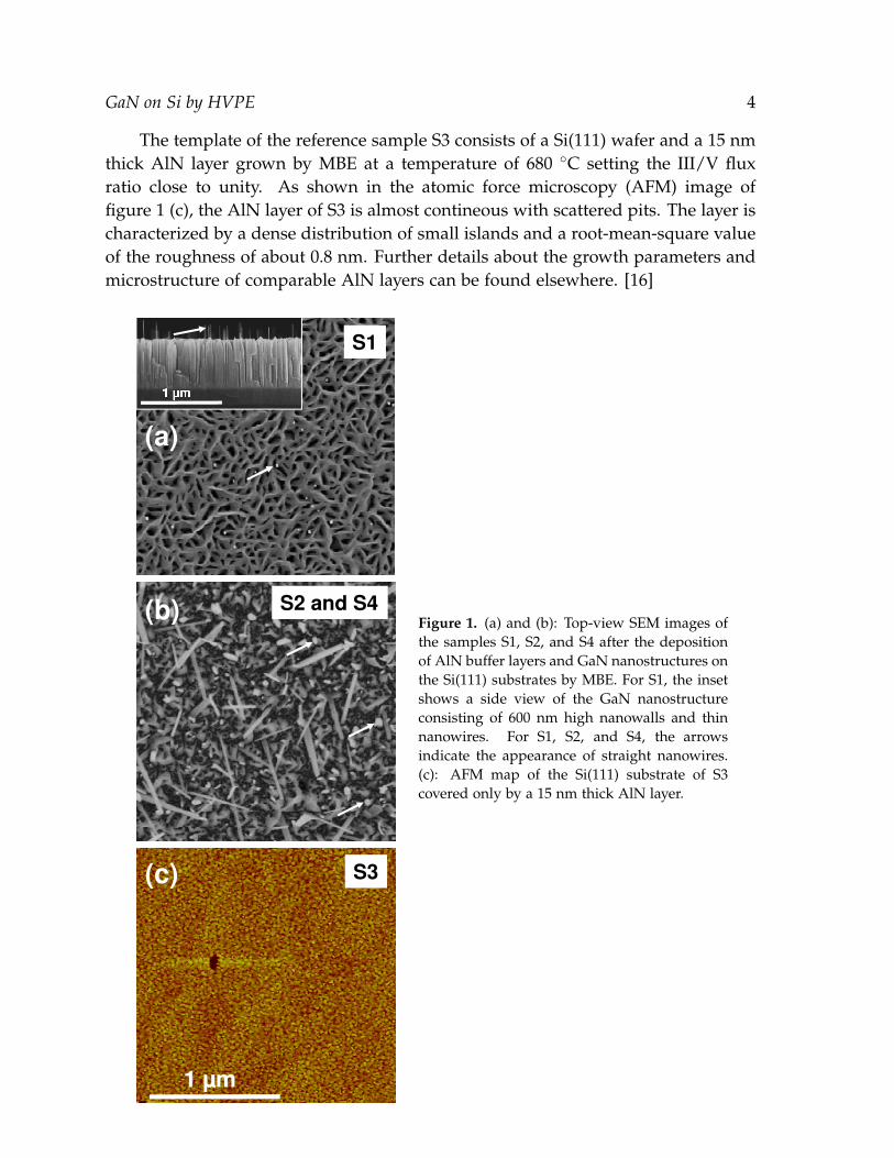
Three templates have been prepared by MBE for the HVPE overgrowth to obtainseveral ten to several hundred µm thick GaN layers on silicon. For sample S1,a commercial Kyma-Si/AlN template consisting of an n-type Si(111) wafer and a200 nm thick Al-face AlN buffer layer have been used. On top of this template, GaNhas been deposited by MBE at a temperature of 800 ◦C setting the III/V flux ratio to0.5. As a result, we obtained GaN nanostructures consisting of highly dense 0.6 µmhigh nano-walls and of taller nano-wires (NW) with a low density as shown in theSEM image of S1 in figure 1 (a) and indicated by white arrows in the top view andcross-sectional image of figure 1 (a). The very thin GaN NWs visible in figure 1 (a),which emerge from the GaN matrix, resemble a lot the ones observed by FernandezGarrido et al. [15] on high quality Al-polar AlN layers grown on SiC (0001). For thisreason we believe that the results obtained by Fernandez Garrido et al. are also validfor sample S1, that is the very thin GaN NWs are N-polar, whereas the GaN matrixis Ga-polar.
The template of samples S2 and S4 consisted of an n-type Si(111) wafer anda 25 nm thick AlN buffer layer grown by MBE at a temperature of 680 ◦C witha III/V flux ratio close to unity. This Si/AlN template was transferred to anotherMBE chamber to add GaN nanostructures, which have been grown at 780 ◦C usinga III/V flux ratio of 0.31. The resulting nanostructures consist of a rough parasiticlayer, straight NWs with low density, and a large density of tilted nano-leafs [cf.SEM image of S2 and S4 in figure 1 (b)].
GaN on Si by HVPE 4
The template of the reference sample S3 consists of a Si(111) wafer and a 15 nmthick AlN layer grown by MBE at a temperature of 680 ◦C setting the III/V fluxratio close to unity. As shown in the atomic force microscopy (AFM) image offigure 1 (c), the AlN layer of S3 is almost contineous with scattered pits. The layer ischaracterized by a dense distribution of small islands and a root-mean-square valueof the roughness of about 0.8 nm. Further details about the growth parameters andmicrostructure of comparable AlN layers can be found elsewhere. [16]
Figure 1. (a) and (b): Top-view SEM images ofthe samples S1, S2, and S4 after the depositionof AlN buffer layers and GaN nanostructures onthe Si(111) substrates by MBE. For S1, the insetshows a side view of the GaN nanostructureconsisting of 600 nm high nanowalls and thinnanowires. For S1, S2, and S4, the arrowsindicate the appearance of straight nanowires.(c): AFM map of the Si(111) substrate of S3covered only by a 15 nm thick AlN layer.
GaN on Si by HVPE 5
2.2. HVPE overgrowth
The described templates showing very different surface structures were overgrownby thick GaN layers using a home-made horizontal reactor HVPE system. Duringthe GaN growth, N2 and H2 were used as a carrier gas with a ratio of 1:1. Thetemperature of the Ga boat was set to about 850 ◦C. The samples S1 to S3 wereovergrown separately, but using the same conditions. We applied a two-step growthmode approach, which consisted of a low-T (800 ◦C) and a subsequent high-T(950 ◦C) step. During the first HVPE step, a lower temperature together with lowHCl and NH3 fluxes have been chosen in order to prevent the evolution of silicon-melt-back etching. The HCl and NH3 fluxes amounted to 0.01 and 0.6 slm duringthe first step and to 0.04 and 1.8 slm during the second step. For S1 and S2–S4,the growth time of the low-T step amounted to 20 and 50 minutes, respectively.The high-T step lasted for 30 minutes for all samples. In the case of sample S4, anadditional 360 minutes long high-T step has been performed at 1063 ◦C in orderto obtain a GaN substrate of several hundred µm thickness. In order to provide amore clear overview of the layer parameters and growth conditions, we summarizethe thickness values of the used AlN buffers and of the HVPE GaN layers as well asthe HVPE growth temperatures and corresponding growth times of the samples S1to S4 in Table 1.
Sample S1 S2 S3 S4dAlN (nm) 200 25 15 25TG1 (◦C), tG1 (min.) 800, 20 800, 50 800, 50 800, 50d1 (µm) 5 10 — —TG2 (◦C), tG2 (min.) 950, 30 950, 30 950, 30 950, 30TG3 (◦C), tG3 (min.) — — — 1063, 360dtotal (µm) 25 40 25 600
Table 1. Thickness of the AlN buffer layer (dAlN) grown by MBE, growthtemperature and time of the low-T HVPE step (TG1 and tG1), growth temperatureand time of the high-T HVPE steps (TG2 and tG2, TG3 and tG3), thickness of the GaNlayer after the low-T HVPE step (d1), and total thickness of the HVPE GaN (dtotal)for the samples S1 to S4.
2.3. Analysis
The morphology of all of these samples was imaged by means of a field-emissionSEM or by means of an AFM. The spatial distribution of the luminescence intensityas well as luminescence spectra from the cross-sections of the overgrown GaN layerswere measured using a CL system attached to the SEM. The cross-sections wereprepared by using an Ar-ion cutting machine. SEM and monochromatic CL images
GaN on Si by HVPE 6
were acquired simultaneously for an accurate assignment of the local origin of theCL. A He-cooling stage allowed to vary the sample temperatures between 6 and 300K. The CL system was operated with a photomultiplier tube for both monochromaticimaging and to record CL spectra. For the acquisition of both CL spectra and CLimages, the acceleration voltage and the current of the electron beam were chosento be 5 kV and about 1 nA, respectively.
3. Results and discussion
3.1. Surface morphology and luminescence spectra of S1–S3
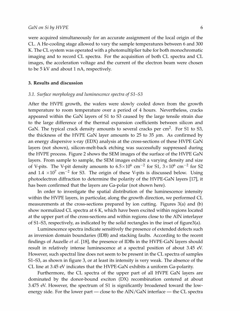
After the HVPE growth, the wafers were slowly cooled down from the growthtemperature to room temperature over a period of 4 hours. Nevertheless, cracksappeared within the GaN layers of S1 to S3 caused by the large tensile strain dueto the large difference of the thermal expansion coefficients between silicon andGaN. The typical crack density amounts to several cracks per cm2. For S1 to S3,the thickness of the HVPE GaN layer amounts to 25 to 35 µm. As confirmed byan energy dispersive x-ray (EDX) analysis at the cross-sections of these HVPE GaNlayers (not shown), silicon-melt-back etching was successfully suppressed duringthe HVPE process. Figure 2 shows the SEM images of the surface of the HVPE GaNlayers. From sample to sample, the SEM images exhibit a varying density and sizeof V-pits. The V-pit density amounts to 6.5×106 cm−2 for S1, 3×106 cm−2 for S2and 1.4 ×107 cm−2 for S3. The origin of these V-pits is discussed below. Usingphotoelectron diffraction to determine the polarity of the HVPE-GaN layers [17], ithas been confirmed that the layers are Ga-polar (not shown here).
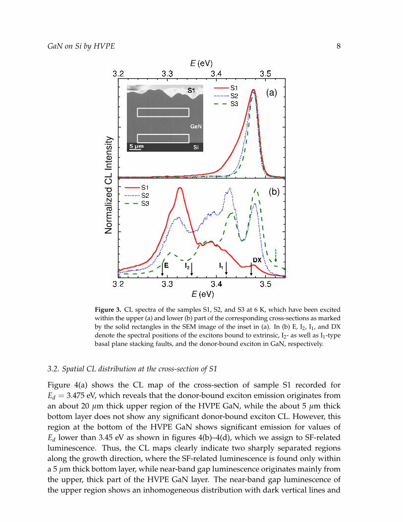
In order to investigate the spatial distribution of the luminescence intensitywithin the HVPE layers, in particular, along the growth direction, we performed CLmeasurements at the cross-sections prepared by ion cutting. Figures 3(a) and (b)show normalized CL spectra at 6 K, which have been excited within regions locatedat the upper part of the cross-sections and within regions close to the AlN interlayerof S1–S3, respectively, as indicated by the solid rectangles in the inset of figure3(a).
Luminescence spectra indicate sensitively the presence of extended defects suchas inversion domain boundaries (IDB) and stacking faults. According to the recentfindings of Auzelle et al. [18], the presence of IDBs in the HVPE-GaN layers shouldresult in relatively intense luminescence at a spectral position of about 3.45 eV.However, such spectral line does not seem to be present in the CL spectra of samplesS1–S3, as shown in figure 3, or at least its intensity is very weak. The absence of theCL line at 3.45 eV indicates that the HVPE-GaN exhibits a uniform Ga-polarity.
Furthermore, the CL spectra of the upper part of all HVPE GaN layers aredominated by the donor-bound exciton (DX) recombination centered at about3.475 eV. However, the spectrum of S1 is significantly broadened toward the low-energy side. For the lower part — close to the AlN/GaN interface — the CL spectra
GaN on Si by HVPE 7
Figure 2. (a)–(c): Top-view SEM imagesof the samples S1–S3, respectively, after theovergrowth of the templates shown in Fig. 1 byseveral ten µm of GaN using HVPE.
of S1 and S2 are dominated by luminescence lines centered at energy values below3.44 eV. We assign these lines to excitons bound to basal plane stacking faults (I1 SF,I2 SF, and E SF). [19, 20] For sample S3, the CL spectrum of the lower part of thecross-section shows also significant contributions of SF-related luminescence, whichare not as dominant as in S1 and S2. In contrast to S1 and S2, the CL spectrum ofthe lower part of S3 clearly shows a shoulder at an energy value exceeding the oneof the GaN band edge [cf. dashed arrow in figure 3(b)]. As will be discussed below,the origin of this high-energy shoulder could be a high unintentional doping of theGaN layer close to the Si/GaN interface due to silicon incorporation.
The spatial origin of the various parts of the CL spectra can be preciselydetermined by acquiring CL maps for the corresponding CL detection energies Ed.The ion-milled edges of the samples show smooth surfaces [cf. inset of figure 3(a)]allowing for a mapping of the CL intensity without artifacts caused by a roughtopography due to a typically non-uniform cleavage of GaN.
GaN on Si by HVPE 8
Figure 3. CL spectra of the samples S1, S2, and S3 at 6 K, which have been excitedwithin the upper (a) and lower (b) part of the corresponding cross-sections as markedby the solid rectangles in the SEM image of the inset in (a). In (b) E, I2, I1, and DXdenote the spectral positions of the excitons bound to extrinsic, I2- as well as I1-typebasal plane stacking faults, and the donor-bound exciton in GaN, respectively.
3.2. Spatial CL distribution at the cross-section of S1
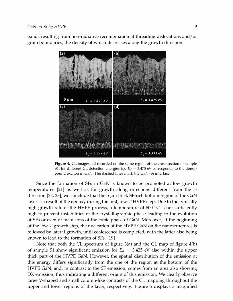
Figure 4(a) shows the CL map of the cross-section of sample S1 recorded forEd = 3.475 eV, which reveals that the donor-bound exciton emission originates froman about 20 µm thick upper region of the HVPE GaN, while the about 5 µm thickbottom layer does not show any significant donor-bound exciton CL. However, thisregion at the bottom of the HVPE GaN shows significant emission for values ofEd lower than 3.45 eV as shown in figures 4(b)–4(d), which we assign to SF-relatedluminescence. Thus, the CL maps clearly indicate two sharply separated regionsalong the growth direction, where the SF-related luminescence is found only withina 5 µm thick bottom layer, while near-band gap luminescence originates mainly fromthe upper, thick part of the HVPE GaN layer. The near-band gap luminescence ofthe upper region shows an inhomogeneous distribution with dark vertical lines and
GaN on Si by HVPE 9
bands resulting from non-radiative recombination at threading dislocations and/orgrain boundaries, the density of which decreases along the growth direction.
Figure 4. CL images, all recorded on the same region of the cross-section of sampleS1, for different CL detection energies Ed. Ed = 3.475 eV corresponds to the donor-bound exciton in GaN. The dashed lines mark the GaN/Si interface.
Since the formation of SFs in GaN is known to be promoted at low growthtemperatures [21] as well as for growth along directions different from the c-direction [22, 23], we conclude that the 5 µm thick SF-rich bottom region of the GaNlayer is a result of the epitaxy during the first, low-T HVPE step. Due to the typicallyhigh growth rate of the HVPE process, a temperature of 800 ◦C is not sufficientlyhigh to prevent instabilities of the crystallographic phase leading to the evolutionof SFs or even of inclusions of the cubic phase of GaN. Moreover, at the beginningof the low-T growth step, the nucleation of the HVPE GaN on the nanostructures isfollowed by lateral growth, until coalescence is completed, with the latter also beingknown to lead to the formation of SFs. [19]
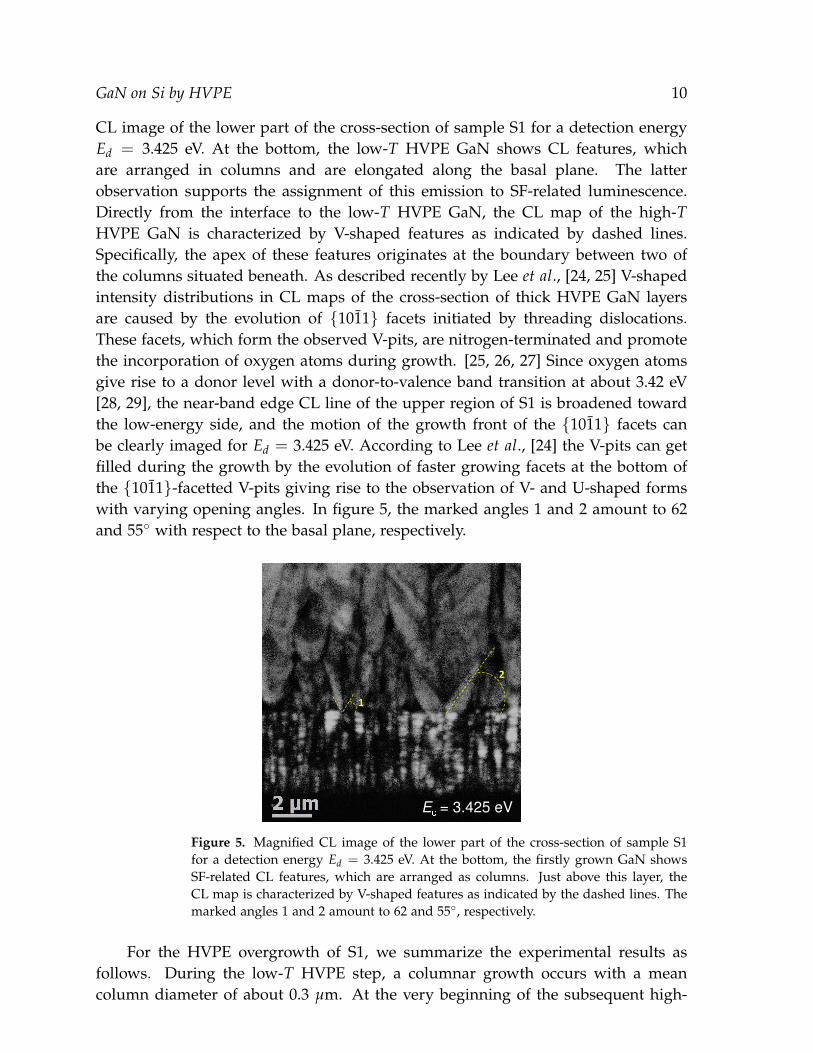
Note that both the CL spectrum of figure 3(a) and the CL map of figure 4(b)of sample S1 show significant emission for Ed = 3.425 eV also within the upperthick part of the HVPE GaN. However, the spatial distribution of the emission atthis energy differs significantly from the one of the region at the bottom of theHVPE GaN, and, in contrast to the SF emission, comes from an area also showingDX emission, thus indicating a different origin of this emission. We clearly observelarge V-shaped and small column-like contrasts of the CL mapping throughout theupper and lower regions of the layer, respectively. Figure 5 displays a magnified
GaN on Si by HVPE 10
CL image of the lower part of the cross-section of sample S1 for a detection energyEd = 3.425 eV. At the bottom, the low-T HVPE GaN shows CL features, whichare arranged in columns and are elongated along the basal plane. The latterobservation supports the assignment of this emission to SF-related luminescence.Directly from the interface to the low-T HVPE GaN, the CL map of the high-THVPE GaN is characterized by V-shaped features as indicated by dashed lines.Specifically, the apex of these features originates at the boundary between two ofthe columns situated beneath. As described recently by Lee et al., [24, 25] V-shapedintensity distributions in CL maps of the cross-section of thick HVPE GaN layersare caused by the evolution of {1011} facets initiated by threading dislocations.These facets, which form the observed V-pits, are nitrogen-terminated and promotethe incorporation of oxygen atoms during growth. [25, 26, 27] Since oxygen atomsgive rise to a donor level with a donor-to-valence band transition at about 3.42 eV[28, 29], the near-band edge CL line of the upper region of S1 is broadened towardthe low-energy side, and the motion of the growth front of the {1011} facets canbe clearly imaged for Ed = 3.425 eV. According to Lee et al., [24] the V-pits can getfilled during the growth by the evolution of faster growing facets at the bottom ofthe {1011}-facetted V-pits giving rise to the observation of V- and U-shaped formswith varying opening angles. In figure 5, the marked angles 1 and 2 amount to 62and 55◦ with respect to the basal plane, respectively.
Figure 5. Magnified CL image of the lower part of the cross-section of sample S1for a detection energy Ed = 3.425 eV. At the bottom, the firstly grown GaN showsSF-related CL features, which are arranged as columns. Just above this layer, theCL map is characterized by V-shaped features as indicated by the dashed lines. Themarked angles 1 and 2 amount to 62 and 55◦, respectively.
For the HVPE overgrowth of S1, we summarize the experimental results asfollows. During the low-T HVPE step, a columnar growth occurs with a meancolumn diameter of about 0.3 µm. At the very beginning of the subsequent high-
GaN on Si by HVPE 11
T HVPE step, V-pits evolve, the growth dynamics of which are governed by facetgrowth leading to an increase of the concentration of incorporated impurity atomssuch as oxygen.
3.3. Spatial CL distribution at the cross-section of S2
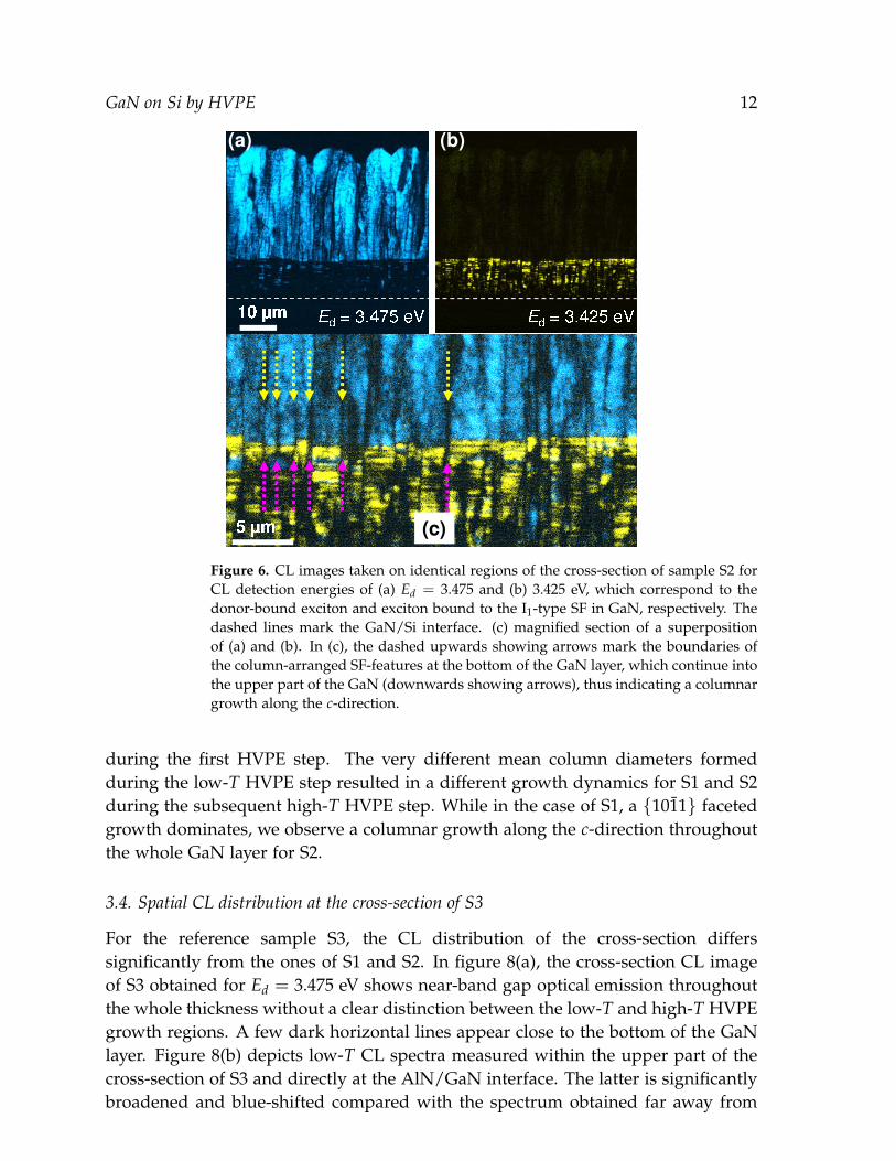
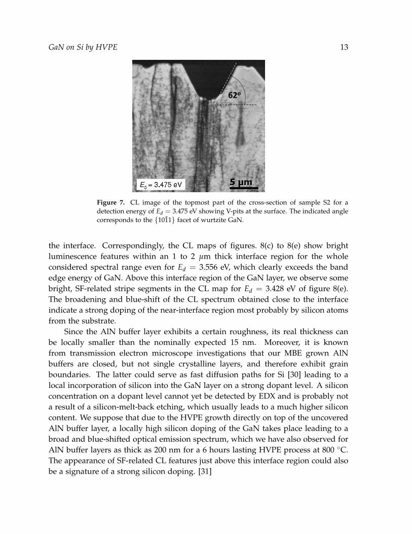
Figures 6(a) and 6(b) show CL images of identical regions from the cross-section ofsample S2 for CL detection energies of Ed = 3.475 and 3.425 eV, respectively. Again,we observe two distinct parts of the HVPE GaN representing the HVPE grown atlow T and high T, where the optical emission of the former is related to basalplane SFs, while the emission of the latter is related to the donor-bound exciton inGaN. Moreover, the CL distribution mapped at 3.425 eV is very weak throughoutthe whole upper part of the HVPE GaN and does not show any significant featuressuch as V-shaped patterns. An enlarged section of the superposition of the CL mapsof figures 6(a) and 6(b) is shown in figure 6(c) for a direct correlation. In the lowerpart of figure 6(c), the CL intensity forms stripe segments oriented along the basalplane confirming again their basal plane SF-related origin. These stripe segments arearranged within columns with an average diameter of 2 µm, the borders of whichare continued within the upper part of figure 6(c) (cf. dashed arrows) indicating acolumnar growth of the GaN along the c-direction during the high-T HVPE step.Some of the dark border lines are disappearing along the growth direction dueto coalescence of neighboring columns. We do not observe any indication of theevolution of {1011} or other slowly growing facets, i. e., of a V-pit-like growth atthis stage of the epitaxy. Nevertheless, V-pits are also present at the surface of S2 asvisible in figure 6(a) and shown in figure 2(b). These V-pits were, however, formedwithin a region close to the surface, where either a bundle of or single dark-linedefects are found at their apex as shown in the CL image of figure 7. The indicatedangle of 62◦ corresponds to {1011} facets.
A reason for the appearance of the V-pits at the surface could be a non-uniform decomposition of the GaN during cooling down to room temperature afterthe HVPE has been terminated. Since the cooling rate is usually low in orderto minimize cracking of the layer, the sample remains for a long time at hightemperatures. If the decomposition rate is higher at positions, where threadingdislocations penetrate the surface, compared with the surrounding surface regions,V-pits can be formed at dislocation positions as shown in figure 7.
Comparing the above discussed CL data of S1 and S2, we assume that thedifferent morphology of the underlying MBE-grown nanostructure (cf. figure 1),where the density of the nanowalls of S1 is much higher than the density of NWsor nanoleafs of S2, resulted in a columnar growth with very different mean columndiameters (0.3 µm for S1 and 2 µm for S2) during the low-T HVPE step. Accordingto Kwon et al. [14], a larger distance of the nanostructures serving as the template fora HVPE overgrowth promotes a lateral epitaxy and therefore results in larger grains
GaN on Si by HVPE 12
Figure 6. CL images taken on identical regions of the cross-section of sample S2 forCL detection energies of (a) Ed = 3.475 and (b) 3.425 eV, which correspond to thedonor-bound exciton and exciton bound to the I1-type SF in GaN, respectively. Thedashed lines mark the GaN/Si interface. (c) magnified section of a superpositionof (a) and (b). In (c), the dashed upwards showing arrows mark the boundaries ofthe column-arranged SF-features at the bottom of the GaN layer, which continue intothe upper part of the GaN (downwards showing arrows), thus indicating a columnargrowth along the c-direction.
during the first HVPE step. The very different mean column diameters formedduring the low-T HVPE step resulted in a different growth dynamics for S1 and S2during the subsequent high-T HVPE step. While in the case of S1, a {1011} facetedgrowth dominates, we observe a columnar growth along the c-direction throughoutthe whole GaN layer for S2.
3.4. Spatial CL distribution at the cross-section of S3
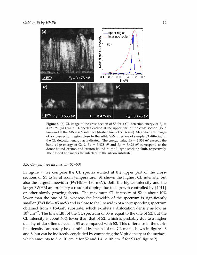
For the reference sample S3, the CL distribution of the cross-section differssignificantly from the ones of S1 and S2. In figure 8(a), the cross-section CL imageof S3 obtained for Ed = 3.475 eV shows near-band gap optical emission throughoutthe whole thickness without a clear distinction between the low-T and high-T HVPEgrowth regions. A few dark horizontal lines appear close to the bottom of the GaNlayer. Figure 8(b) depicts low-T CL spectra measured within the upper part of thecross-section of S3 and directly at the AlN/GaN interface. The latter is significantlybroadened and blue-shifted compared with the spectrum obtained far away from
GaN on Si by HVPE 13
Figure 7. CL image of the topmost part of the cross-section of sample S2 for adetection energy of Ed = 3.475 eV showing V-pits at the surface. The indicated anglecorresponds to the {1011} facet of wurtzite GaN.
the interface. Correspondingly, the CL maps of figures. 8(c) to 8(e) show brightluminescence features within an 1 to 2 µm thick interface region for the wholeconsidered spectral range even for Ed = 3.556 eV, which clearly exceeds the bandedge energy of GaN. Above this interface region of the GaN layer, we observe somebright, SF-related stripe segments in the CL map for Ed = 3.428 eV of figure 8(e).The broadening and blue-shift of the CL spectrum obtained close to the interfaceindicate a strong doping of the near-interface region most probably by silicon atomsfrom the substrate.
Since the AlN buffer layer exhibits a certain roughness, its real thickness canbe locally smaller than the nominally expected 15 nm. Moreover, it is knownfrom transmission electron microscope investigations that our MBE grown AlNbuffers are closed, but not single crystalline layers, and therefore exhibit grainboundaries. The latter could serve as fast diffusion paths for Si [30] leading to alocal incorporation of silicon into the GaN layer on a strong dopant level. A siliconconcentration on a dopant level cannot yet be detected by EDX and is probably nota result of a silicon-melt-back etching, which usually leads to a much higher siliconcontent. We suppose that due to the HVPE growth directly on top of the uncoveredAlN buffer layer, a locally high silicon doping of the GaN takes place leading to abroad and blue-shifted optical emission spectrum, which we have also observed forAlN buffer layers as thick as 200 nm for a 6 hours lasting HVPE process at 800 ◦C.The appearance of SF-related CL features just above this interface region could alsobe a signature of a strong silicon doping. [31]
GaN on Si by HVPE 14
Figure 8. (a) CL image of the cross-section of S3 for a CL detection energy of Ed =3.475 eV. (b) Low-T CL spectra excited at the upper part of the cross-section (solidline) and at the AlN/GaN interface (dashed line) of S3. (c)–(e): Magnified CL imagesof a cross-section region close to the AlN/GaN interface of sample S3 differing inthe CL detection energy as indicated. The energy value Ed = 3.556 eV exceeds theband edge energy of GaN. Ed = 3.475 eV and Ed = 3.428 eV correspond to thedonor-bound exciton and exciton bound to the I1-type stacking fault, respectively.The dashed line marks the interface to the silicon substrate.
3.5. Comparative discussion (S1–S3)
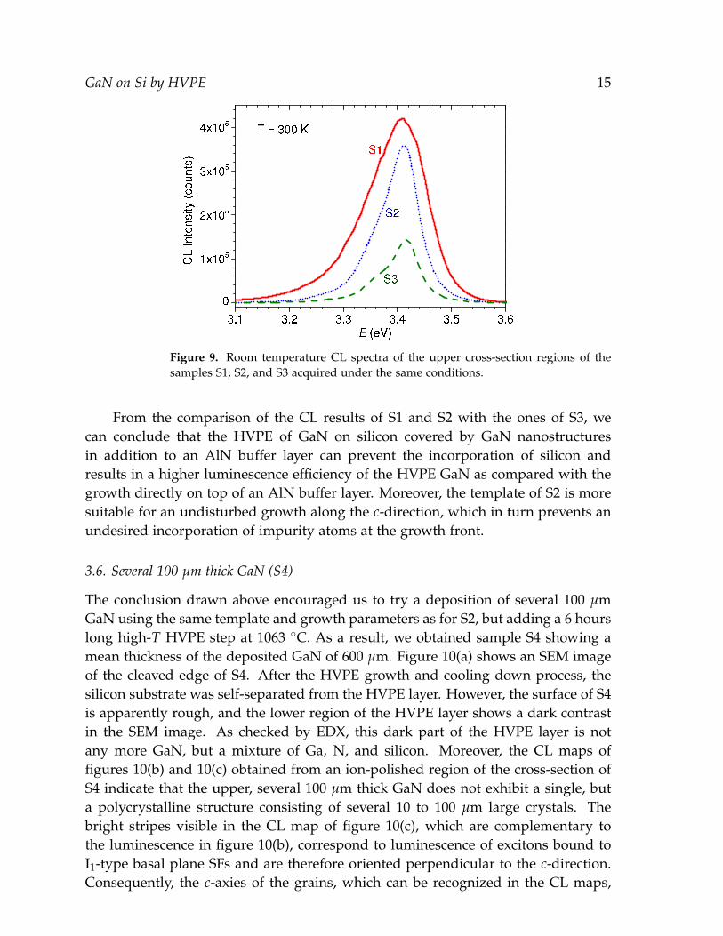
In figure 9, we compare the CL spectra excited at the upper part of the cross-sections of S1 to S3 at room temperature. S1 shows the highest CL intensity, butalso the largest linewidth (FWHM= 130 meV). Both the higher intensity and thelarger FWHM are probably a result of doping due to a growth controlled by {1011}or other slowly growing facets. The maximum CL intensity of S2 is about 10%lower than the one of S1, whereas the linewidth of the spectrum is significantlysmaller (FWHM= 85 meV) and is close to the linewidth of a corresponding spectrumobtained from a FS-GaN substrate, which exhibits a dislocation density as low as106 cm−2. The linewidth of the CL spectrum of S3 is equal to the one of S2, but theCL intensity is about 60% lower than that of S2, which is probably due to a higherdensity of dark-line defects in S3 as compared with S2. This difference in the dark-line density can hardly be quantified by means of the CL maps shown in figures. 6and 8, but can be indirectly concluded by comparing the V-pit density at the surface,which amounts to 3× 106 cm−2 for S2 and 1.4 × 107 cm−2 for S3 (cf. figure 2).
GaN on Si by HVPE 15
Figure 9. Room temperature CL spectra of the upper cross-section regions of thesamples S1, S2, and S3 acquired under the same conditions.
From the comparison of the CL results of S1 and S2 with the ones of S3, wecan conclude that the HVPE of GaN on silicon covered by GaN nanostructuresin addition to an AlN buffer layer can prevent the incorporation of silicon andresults in a higher luminescence efficiency of the HVPE GaN as compared with thegrowth directly on top of an AlN buffer layer. Moreover, the template of S2 is moresuitable for an undisturbed growth along the c-direction, which in turn prevents anundesired incorporation of impurity atoms at the growth front.
3.6. Several 100 µm thick GaN (S4)
The conclusion drawn above encouraged us to try a deposition of several 100 µmGaN using the same template and growth parameters as for S2, but adding a 6 hourslong high-T HVPE step at 1063 ◦C. As a result, we obtained sample S4 showing amean thickness of the deposited GaN of 600 µm. Figure 10(a) shows an SEM imageof the cleaved edge of S4. After the HVPE growth and cooling down process, thesilicon substrate was self-separated from the HVPE layer. However, the surface of S4is apparently rough, and the lower region of the HVPE layer shows a dark contrastin the SEM image. As checked by EDX, this dark part of the HVPE layer is notany more GaN, but a mixture of Ga, N, and silicon. Moreover, the CL maps offigures 10(b) and 10(c) obtained from an ion-polished region of the cross-section ofS4 indicate that the upper, several 100 µm thick GaN does not exhibit a single, buta polycrystalline structure consisting of several 10 to 100 µm large crystals. Thebright stripes visible in the CL map of figure 10(c), which are complementary tothe luminescence in figure 10(b), correspond to luminescence of excitons bound toI1-type basal plane SFs and are therefore oriented perpendicular to the c-direction.Consequently, the c-axies of the grains, which can be recognized in the CL maps,
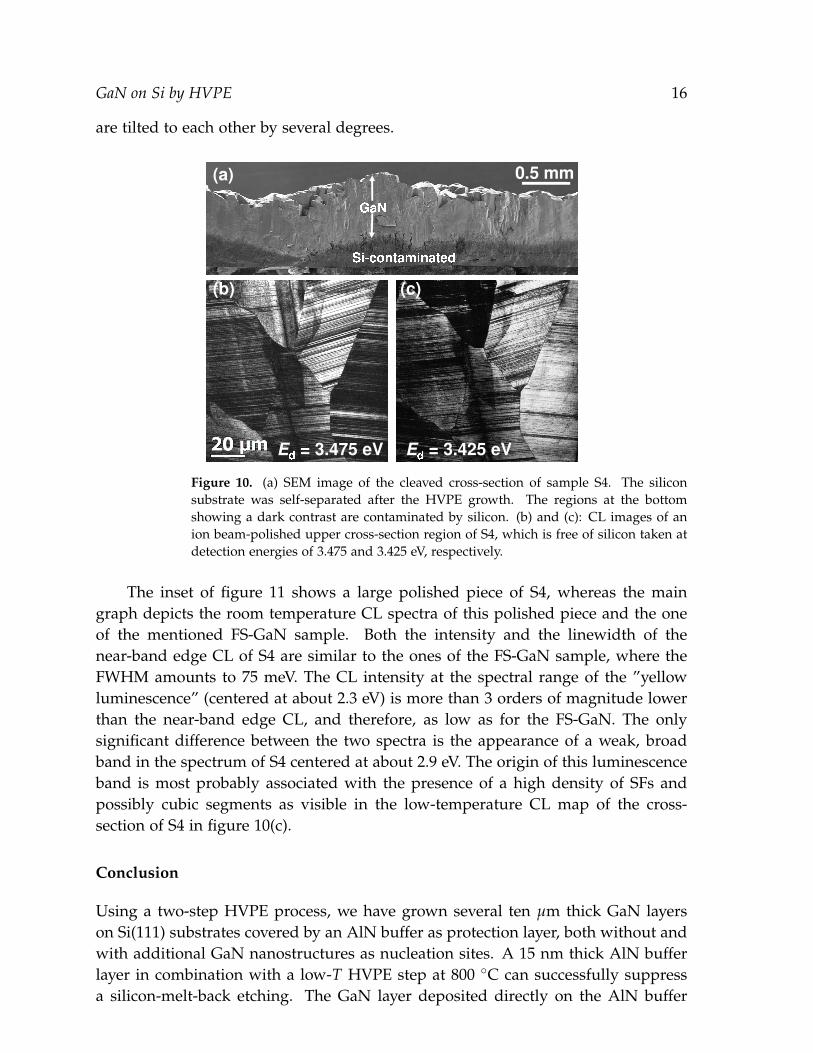
GaN on Si by HVPE 16
are tilted to each other by several degrees.
Figure 10. (a) SEM image of the cleaved cross-section of sample S4. The siliconsubstrate was self-separated after the HVPE growth. The regions at the bottomshowing a dark contrast are contaminated by silicon. (b) and (c): CL images of anion beam-polished upper cross-section region of S4, which is free of silicon taken atdetection energies of 3.475 and 3.425 eV, respectively.
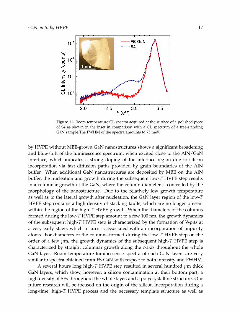
The inset of figure 11 shows a large polished piece of S4, whereas the maingraph depicts the room temperature CL spectra of this polished piece and the oneof the mentioned FS-GaN sample. Both the intensity and the linewidth of thenear-band edge CL of S4 are similar to the ones of the FS-GaN sample, where theFWHM amounts to 75 meV. The CL intensity at the spectral range of the ”yellowluminescence” (centered at about 2.3 eV) is more than 3 orders of magnitude lowerthan the near-band edge CL, and therefore, as low as for the FS-GaN. The onlysignificant difference between the two spectra is the appearance of a weak, broadband in the spectrum of S4 centered at about 2.9 eV. The origin of this luminescenceband is most probably associated with the presence of a high density of SFs andpossibly cubic segments as visible in the low-temperature CL map of the cross-section of S4 in figure 10(c).
Conclusion
Using a two-step HVPE process, we have grown several ten µm thick GaN layerson Si(111) substrates covered by an AlN buffer as protection layer, both without andwith additional GaN nanostructures as nucleation sites. A 15 nm thick AlN bufferlayer in combination with a low-T HVPE step at 800 ◦C can successfully suppressa silicon-melt-back etching. The GaN layer deposited directly on the AlN buffer
GaN on Si by HVPE 17
Figure 11. Room temperature CL spectra acquired at the surface of a polished pieceof S4 as shown in the inset in comparison with a CL spectrum of a free-standingGaN sample.The FWHM of the spectra amounts to 75 meV.
by HVPE without MBE-grown GaN nanostructures shows a significant broadeningand blue-shift of the luminescence spectrum, when excited close to the AlN/GaNinterface, which indicates a strong doping of the interface region due to siliconincorporation via fast diffusion paths provided by grain boundaries of the AlNbuffer. When additional GaN nanostructures are deposited by MBE on the AlNbuffer, the nucleation and growth during the subsequent low-T HVPE step resultsin a columnar growth of the GaN, where the column diameter is controlled by themorphology of the nanostructure. Due to the relatively low growth temperatureas well as to the lateral growth after nucleation, the GaN layer region of the low-THVPE step contains a high density of stacking faults, which are no longer presentwithin the region of the high-T HVPE growth. When the diameters of the columnsformed during the low-T HVPE step amount to a few 100 nm, the growth dynamicsof the subsequent high-T HVPE step is characterized by the formation of V-pits ata very early stage, which in turn is associated with an incorporation of impurityatoms. For diameters of the columns formed during the low-T HVPE step on theorder of a few µm, the growth dynamics of the subsequent high-T HVPE step ischaracterized by straight columnar growth along the c-axis throughout the wholeGaN layer. Room temperature luminescence spectra of such GaN layers are verysimilar to spectra obtained from FS-GaN with respect to both intensity and FWHM.
A several hours long high-T HVPE step resulted in several hundred µm thickGaN layers, which show, however, a silicon contamination at their bottom part, ahigh density of SFs throughout the whole layer, and a polycrystalline structure. Ourfuture research will be focused on the origin of the silicon incorporation during along-time, high-T HVPE process and the necessary template structure as well as
GaN on Si by HVPE 18
growth parameters to prevent the reaction of silicon with the HVPE GaN.
Acknowledgments
We thank Oliver Brandt for fruitful discussions and Raffaella Calarco as well asHolger T. Grahn for a careful reading of the manuscript. Moreover, we thank O.Romanyuk for the investigation of the polarity of the HVPE GaN by photoelectrondiffraction and we gratefully acknowledge financial support of this work by theSino-German Center for Science Promotion through the project GZ 736.
References
[1] Xu K, Wang J-F, Ren G-Q 2015 Chin. Phys. B 24 066105[2] Shibata T, Sone H, Yahashi K, Yamaguchi M, Hiramatsu K and Itoh N 1998 J. Cryst. Growth
189/190 67–71[3] Lee H J, Lee S W, Goto H, Lee Hyo-Jong, Ha J S, Cho M W and Yao T 2007 phys. stat. sol. (c) 4
2268–2271[4] Gu S, Zhang R, Shi Y and Zheng Y J 2001 Phys. D: Appl. Phys. 34 1951–1954[5] Honda Y, Okano M, Yamaguchi M and Sawaki N 2005 phys. stat. sol. (c) 2 2125–2128[6] Nishimura Y, Honda Y, Yamaguchi M and Sawaki N 2003 phys. stat. sol. (c) 0 2506–2510[7] Lee H J, Kim K H, Yi J Y, Yang M, Ahn H S, Chang J H, Kim H S, Yi S N, Lee S C, Kim S W,
Honda Y, Yamaguchi M and Sawaki N 2004 J. Korean Phys. Soc. 45 S813–S815[8] Bessolov V N, Davydov V Yu, Zhilyaev Yu V, Konenkova E V, Mosina G N, Raevskii S, Rodin S
N, Sharofidinov Sh, Shcheglov M P, Park H S, and Koike M 2005 Tech. Phys. Lett. 31 915–918[9] Hersee S D, Zubia D, Sun X, Bommena R, Fairchild M, Zhang S, Burckel D, Frauenglass A and
Brueck S R J 2002 IEEE J. Quantum Electron. 38 1017–1028[10] Liang J, Hong S-K, Kouklin N, Beresford R and Xu J M 2003 Appl. Phys. Lett. 83 1752-1754[11] Fu Y, Moon Y T, Yun F, Ozgur U, Xie J Q, Dogan S, Morkoc H, Inoki C K, Kuan T S, Zhou L and
Smith D 2005 J. Appl. Phys. Lett. 86 043108[12] Wang Y D, Zang K Y, Chua S J, Tripathy S, Chen P, and Fonstad C G 2005 Appl. Phys. Lett. 87
251915[13] Chan C-H, Hou C-H, Tseng S-Z, Chen T-J, Chien H-T, Hsiao F-L, Lee C-C, Tsai Y-L and Chen
C-C 2009 Appl. Phys. Lett. 95 011110[14] Kwon H Y, Moon J Y, Choi Y J, Shin M J, Ahn H S, Yang M, Chang J H, Yi S N and Ha D H 2010
Mater. Sci. Eng. B 166 28[15] Fernandez Garrido S, Kong X, Gotschke T, Calarco R, Geelhaar L, Trampert A and Brandt O
2012 Nano Letters 12 6119[16] Musolino M, Tahraoui A, Fernandez-Garrido S, Brandt O, Trampert A, Geelhaar L and Riechert
H 2015 Nanotechnol. 26 085605[17] Romanyuk O, Jiricek P, Paskova T, Bieloshapka I and Bartos I 2013 Appl. Phys. Lett. 103 091601[18] Auzelle T, Haas B, Den Hertog M, Rouviere J-L, Daudin B and Gayral B 2015 Appl. Phys. Lett.
107 051904[19] Lahnemann J, Brandt O, Jahn U, Pfuller C, Roder C, Dogan P, Grosse F, Belabbes A, Bechstedt
F, Trampert A and Geelhaar L 2012 Phys. Rev. B 86 081302(R)[20] Lahnemann J, Jahn U, Brandt O, Flissikowski T, Dogan P and Grahn H T 2014 J. Phys. D 47
423001[21] Renard J, Tourbot G, Sam-Giao D, Bougerol C, Daudin B and Gayral B 2010 Appl. Phys. Lett. 97
081910[22] Mei J, Srinivasan S, Liu R, Ponce F A, Narukawa Y and Mukai T 2006 Appl. Phys. Lett. 88 141912
GaN on Si by HVPE 19
[23] Corfdir P, Ristic J, Lefebvre P, Zhu T, Martin D, Dussaigne A, Ganiere J D, Grandjean N andDeveaud-Pledran B 2009 Appl. Phys. Lett. 94 201115
[24] Lee W, Lee H J, Park S H, Watanabe K, Kumagai K, Yao T, Chang J H and Sekiguchi T 2012 J.Cryst. Growth 351 83–87
[25] Lee W, Watanabe K, Kumagai K, Park S H, Lee H J, Yao T, Chang J H and Sekiguchi T 2012 J.Electron Microsc. 61 25–30
[26] Bu Y, Imade M, Kishimoto H, Yoshimura M, Sasaki T, Kitaoka Y, Isemura M, Mori Y 2011 J.Crystal Growth 327 89
[27] Wei T B, Ma P, Duan R F, Wang J X, Li J M, Liu Zh and Zeng Y P 2007 Mater. Lett. 61 3882–3885[28] Chung B-C and Gershenzon M J 1992 Appl. Phys. 72 651–659[29] Chen G D, Smith M, Lin J Y, Jiang H X, Salvador A, Sverdlov B N, Botchkarv A and Morkoc H
1996 J. Appl. Phys. 79 2675–2683[30] Jakiela R, Barcz A, Dumiszewska E and Jagoda A 2006 phys. stat. sol. (c) 3 1416–1419[31] Molina S I, Sanchez A M, Pacheco F J, Garcıa R, Sanchez-Garcıa M A, Sanchez F J and Calleja E
1999 Appl. Phys. Lett. 74 3362–3364


![DTRA-TR-16-55 · 2018-01-16 · Epitaxy (HVPE) grown GaN substrate (Kyma technology [3]) was employed and the sandwich structure Schottky diode was fabricated, on which both alpha](https://img.pdfslide.net/doc/110x75/5e68acf064787f6a1c16869d/dtra-tr-16-55-2018-01-16-epitaxy-hvpe-grown-gan-substrate-kyma-technology-3.jpg)