Embed Size (px)
Citation preview

INSTITUTE OF PHYSICS PUBLISHING JOURNAL OF MICROMECHANICS AND MICROENGINEERING
J. Micromech. Microeng. 15 (2005) 1917–1924 doi:10.1088/0960-1317/15/10/018
Open-loop versus closed-loop control ofMEMS devices: choices and issuesB Borovic1, A Q Liu2, D Popa1, H Cai2 and F L Lewis1
1 Automatics and Robotics Research Institute, University of Texas at Arlington,Fort Worth, USA2 School of Electrical and Electronic Engineering, Nanyang Technological University,Singapore 639798
E-mail: [email protected]
Received 1 April 2005, in final form 19 July 2005Published 19 August 2005Online at stacks.iop.org/JMM/15/1917
AbstractFrom a controls point of view, micro electromechanical systems (MEMS)can be driven in an open-loop and closed-loop fashion. Commonly, thesedevices are driven open-loop by applying simple input signals. If these inputsignals become more complex by being derived from the system dynamics,we call such control techniques pre-shaped open-loop driving. The ultimatestep for improving precision and speed of response is the introduction offeedback, e.g. closed-loop control. Unlike macro mechanical systems,where the implementation of the feedback is relatively simple, in the MEMScase the feedback design is quite problematic, due to the limited availabilityof sensor data, the presence of sensor dynamics and noise, and the typicallyfast actuator dynamics. Furthermore, a performance comparison betweenopen-loop and closed-loop control strategies has not been properly exploredfor MEMS devices. The purpose of this paper is to present experimentalresults obtained using both open- and closed-loop strategies and to addressthe comparative issues of driving and control for MEMS devices. An opticalMEMS switching device is used for this study. Based on these experimentalresults, as well as computer simulations, we point out advantages anddisadvantages of the different control strategies, address the problems thatdistinguish MEMS driving systems from their macro counterparts, anddiscuss criteria to choose a suitable control driving strategy.
1. Introduction
Functionality of many MEMS devices relies on proper use ofMEMS actuators. Five basic on-chip actuator technologieshave been developed [1]: magnetic, piezoelectric, thermal,optical and electrostatic. Regardless of the applied actuationtechnique, MEMS are typically driven directly in an open-loop fashion by applying simple input control signals.Straightforward and simple driving techniques provide theMEMS designer with the improved device designs as asimple choice to achieving better dynamical behavior. Hence,MEMS actuators have traditionally been gradually modifiedand improved in terms of mechanical design, suitable open-loop driving signals and better area-efficiency [2–4].
On the other hand, the requirements for better dynamicalbehavior of the MEMS devices in terms of both speedof response and precision have resulted in the gradual
introduction of improved controller driving approaches. If thesimple input signal is made more complex by using the systemdynamics, this results in the so-called pre-shaped control[5–7]. The dynamical model of the device is used to constructa pre-shaped input signal that enables the device to achievebetter and faster dynamical performance.
However, pre-shaped driving schemes are sometimesnot enough. The lack of accurate models, fabricationinconsistencies, and lack of repeatability of the deviceparameters, compounded by special requirements on thedynamical behavior, all call for the use of closed-loopcontrol design [7–11]. The first MEMS devices incorporatingfeedback were closed-loop sensors, with the objective ofenhancing measurement accuracy [1]. An increase incomplexity, device integration and sophistication level ofMEMS devices demands equally sophisticated integratedcontrol systems. Unlike macro mechanical systems where
0960-1317/05/101917+08$30.00 © 2005 IOP Publishing Ltd Printed in the UK 1917
B Borovic et al
the implementation of the feedback is relatively simple, itis quite problematic in the MEMS case. The presence ofsensor dynamics, fast high-frequency system dynamics andrequirements for the integration of the control system on theactual MEMS device have introduced additional challengesfor feedback control design.
Both input shaping and closed-loop approachessignificantly improve the dynamical behavior of MEMS.However, both strategies have their own advantages anddisadvantages. The choice of driving strategy depends onseveral factors—the purpose of the device, complexity of thesensor implementation, available space, complexity of theelectronic circuitry, dynamics of the device and sensitivityof the dynamical response to the device parameters.
The purpose of this paper is to compare and contrastopen-loop and closed-loop design of MEMS control systems,detailing the design issues and choices. We use experimentalresults obtained from implementing pre-shaped open-loop andclosed-loop control methods. We compare the two approachesand point out the advantages and disadvantages of both.It is found that with minimum additional implementationcomplexity, the closed-loop approach speeds up the systemand improves its dynamical response. We also discuss criteriafor choosing between the two control approaches, analyzingparameter sensitivity. As a case study, an optical MEMSdevice (MOEMS) actuated by the electrostatic comb drive [12]was used. The actuator shuttle has a light-modulating shutterattached to it. Optical feedback was used to reconstruct theposition of the shuttle, which cannot be directly measured.The device can be used both as an optical switch (OS) and avariable optical attenuator (VOA) [13–15].
The description of the actual device is given in section 2,a short overview of its mathematical model in section 3, andan experimental analysis of open- and closed-loop approachesis given in section 4. Discussion on small scale feedback,sensing and the choice of driving strategy is given in section 5.At the end, some conclusions are drawn.
2. System description
A MOEMS device similar to the actual device analyzed in thispaper is shown in figure 1. Detailed geometry of the device isgiven in figure 2 [14]. The device was fabricated using deepreactive ion etching (DRIE) [16] on SOI wafers with a 75 µmthick structural layer.
The device consists of two electrostatic comb driveactuators, a suspension mechanism, the body of the devicealso called a shuttle, and a shutter. A voltage applied to thecomb drive actuator generates a force that moves the shuttle.The shutter which is attached to the shuttle then cuts andmodulates a light beam.
The shuttle consists of the shutter and comb supportframes, 508 µm and 1430 µm long respectively. Supportframes are made lighter by creating cavities in the structures(see figure 2). The widths of all features of the shuttle are2 µm. The shutter itself is 3 µm wide and 190 µm long.There are 158 fingers on the comb drive each having a widthof 2 µm and a length of 27 um. The gap between the fingersis 2.5 µm with an initial overlapping of 5 µm. The widthof the folded beams of the suspension is 3 µm with lengths
Figure 1. SEM image of the MEMS VOA showing electrostaticcomb drive, moving shuttle with attached shutter, and optical fiberchannels.
Figure 2. Design and geometry of the device from figure 1.
862.5 µm and 854.5 µm for the outer and inner beams,respectively.
The experimental setup is shown in figure 3. The voltageapplied to the actuator is separated and distributed to bothforward (Vf ) and backward (Vb) combs. The movement of theactuator modulates the light generated by the laser diode andthe light is sensed by the photo-detector. The voltage from thephoto-detector VPD is processed to determine the deflection x.
3. Mathematical model
A simplified model is used to represent the dynamic behaviorof the device. It provides adequate insight and is sufficient forthe purpose of the controller design. The parameters of the
1918

Open-loop versus closed-loop control of MEMS devices
Figure 3. Experimental setup of the VOA.
model are identified analytically, but tuned experimentally.The dynamical model of the system is given as [7, 13, 17]
mx + dx + kx = ff(Vf, x) − fb(Vb, x) (1)
VPD = h(x) (2)
where x is the shutter position, m is the effective movingmass of the shuttle, d is damping, k is the stiffness of thesuspension, ff and fb are the electrostatic forces, VPD is aphoto-detector voltage, and h is a sensing function relatingposition and photo-detector voltage. Driving voltages Vf � 0and Vb � 0 do not overlap in time, e.g. when Vf > 0 ⇒ Vb = 0and Vb < 0 ⇒ Vf = 0. Therefore, we introduce V = Vf + Vb
which will be used frequently throughout this paper. Theparameters of the model (1), (2) that have to be estimated arem, k, d, ff , fb and h(x).
Existing empirical models are readily available to estimateboth effective moving mass and stiffness for structures withtypical suspensions. According to [14] the effective mass ofthe VOA relative to the main degree of freedom (DOF) x canbe expressed as
m = msh + 2.74mb (3)
where msh is the mass of the shuttle and mb is theeffective mass of the eight suspension beams. Taking intoaccount (3), the density of silicon ρSi = 2.3 × 10³ kg m−3 andgeometry given in figure 2, the effective mass of the system ism = 7.75 × 10⁻⁹ kg.
The VOA suspension stiffness is assumed to be linear andis given by [14]
k = 24EIZ/L3 = 2ET (BW)3/(BL)3 (4)
where E is Young’s modulus (E = 160 GPa), BW width ofthe suspension beams, BL is the length of suspension beamsand IZ is the moment of inertia around the deflecting axisof the beam. Calculation, recalling (4) and the geometry infigure 2, gives us k = 1.05 N m−1.
Damping is the most difficult parameter to determineanalytically, even through the use of FEA [18]. The reasonfor this is the number of different complex mechanisms thatcause it, including friction, viscous forces, drag, etc [18, 19].Hence, experimental data are used to estimate damping of thesystem. Assuming that the damping coefficient is unknown,
Figure 4. Open-loop response of the simulated model (10), (11),compared with the experimental one.
but constant, and comparing the simulated and experimentalresponses as shown in figure 4, the damping coefficient turnsout to be d0 = 8 × 10⁻⁵ kg s−1.
Next, the electrical part of the model is derived. Thisderivation was accomplished only for the forward comb drive.However, as experimental results will prove later, it is equallyvalid for the backward force, e.g. ff = fb.
In order to get the model of force acting between thetwo comb drive electrodes, the capacitance of the comb driveas a function of position should be determined first. Thecapacitance is calculated as a sum of parallel capacitancesamong pairs of comb electrodes. The total capacitance, as afunction of position x, is given by [14]
C(x) = ε0A
dG= 2nε0T
dG(x + x0) (5)
where ε0 is the dielectric constant of a vacuum, n is the numberof the movable fingers of the electrode, T is the thicknessof the structural layer, dG is the gap between fingers andx0 is the initial overlapping between the electrodes. Thecapacitance of the comb drive calculated at the rest positionis C(0) = 0.42 pF. It increases as the shuttle moves forwardand decreases as it moves backwards. The electrostatic forcebetween the electrodes of the capacitor is given as [18]
ff(Vf, x) = 1
2V 2
f∂C
∂x(6)
which combined with (5) yields
f (Vf, x) = nε0T
dGV 2
f = keV2
f . (7)
When calculated, the value of the electrostatic constant, ke, is41 nN V−2. Note that the electrostatic force of the comb drivedoes not depend on its deflection. This is a typical property ofcomb drives.
The electrostatic constant (7) can be verified byconducting static experiments (i.e., x = x = 0). Staticconditions reduce (1) and (6) to x = (ke/k)V 2
f yieldingthe experimental deflection–voltage curve shown in figure 5,which fits into x (µm) = −0.081 (µm V−2) V2. Theanalytically obtained value of ke/k turns out to be half of theexperimental value (i.e., −0.039 (µm V−2)). As the stiffness(4) can be determined very accurately, the calculation for ke (7)seems to be inaccurate. The reason for this can be attributedto the finite aspect ratio of the silicon structure fabricated byDRIE, which increases the value of the capacitance (5) several
1919

B Borovic et al
Figure 5. Experimental deflection versus voltage relationship—input nonlinearity of the system.
Figure 6. Optical position measurement [9, 13].
Figure 7. Position–optical intensity characteristics (2)—outputnonlinearity of the system.
times [20]. As a consequence, the experimental results of ke/k
are used in this paper.The maximum static voltages that can be applied to the
electrodes before they exhibit lateral pull-in are V = Vb =−8.75 V and V = Vf = 10.1 V.
The setup for determining the optical model (2) is shownin figures 3 and 6. The light beam is intercepted by theshutter, increasing and decreasing the throughput of thelight. Analytical techniques were developed to determinethe relationship (2) theoretically in [7, 9, 13]. However,due to dissimilarities between the predicted model and anactual experiment, we will rely on experimental results.
The experimentally determined relationship, VPD = h(x),is shown in figure 7.
Experimental data from figure 7 are curve fitted using afourth-order polynomial for 0 � x � 7 µm as
VPD (V) = a4x4 + a3x
3 + a2x2 + a1x + a0 (8)
with the following parameters: a4 = 5.73 × 10⁻⁵ (Vµm−4),a3 = −0.0024 (Vµm−3), a2 = 0.018 (Vµm−2), a1 =
0.03 (Vµm−1) and a0 = −0.69 (V). The light intensity islinearly related to the VPD with its minimum corresponding toVPD = −800 mV and its maximum corresponding to 0 mV.
In order to reconstruct the position from the optical power,which is necessary to measure the deflection, the inverse of (2)has to be determined. The inverse of (2) inside the interval−0.7 V � VPD � −0.3 V, and for x � 0, can be approximatedusing a third-order polynomial as
x∗(µm) = b3V3
PD + b2V2
PD + b1VPD + b0 (9)
where b3 = 116 (µm V−3), b2 = 175.5 (µm V−2), b1 =100 (µm V−1) and b0 = 23.6 (µm).
In summary, the model (1), (2) can be populated byparameters by putting together the results calculated from (3),(4), (7), (8) and figure 4. The complete model is given as
7.75 × 10⁻⁹x + 8 × 10⁻⁵x + 1.05x = 8.2 × 10⁻⁸ V2 (10)
VPD = 5.73 × 1019x4 − 2.4 × 1015x3 + 1.8 × 1010x2
+ 3 × 10⁴x − 0.69. (11)
Note that the deflection x from (10) and (11) is expressed inmeters. The model given in (10) and (11) closely matchesexperimental results. The simulated and experimental open-loop step responses are shown in figure 4.
4. Open- versus closed-loop control
In this section, the comparison between the pre-shaped open-loop and closed-loop driving approaches is given for the actualdevice. Both experimental and computer simulated results areused to illustrate the differences. The simulated results werebased on model (10), (11). Simulations were accomplishedin MATLAB/SIMULINK. Experimental data were collectedusing a Tektronix TDS 2014 oscilloscope. The control systemwas implemented using a dSpace 1104 fast control prototypingsystem.
4.1. Open-loop strategies
Direct open-loop driving of the actuator is straightforward.An applied voltage step causes deflection of the actuator. Theresulting step response is shown in figure 4. The rise timeis 190 µs and the overshoot is 17%. The settling time isapproximately 550 µs.
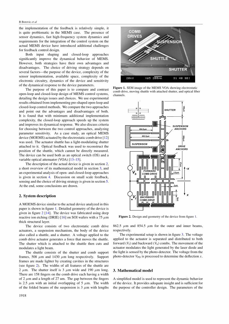
Next, the simple step input signal is modified resulting inpre-shaped open-loop driving. The idea behind pre-shapingis to obtain a faster, aperiodic dynamic response. Here,different voltage pulses are combined to obtain a signal witha high voltage spike at the beginning and a trailing steady-state voltage as shown in figure 8. A zero-voltage periodexists between the initial spike and the steady-state voltage.The signal is defined by the amplitude of the initial spike,the steady-state voltage and the values of the three triggeringinstants. Triggering instants define the beginning and the endof the initial spike as well as the beginning of the steady-statevoltage value.
For a specified steady-state voltage and a given maximumamplitude of the voltage spike, this input signal will givethe fastest possible aperiodic response. The rise time of theresponse is determined by the difference between the third
1920
Open-loop versus closed-loop control of MEMS devices
Figure 8. Pre-shaped open-loop response, all signals have the samevoltage level (simulation results).
Figure 9. Cascaded multivibrators and summing op-amp forassembling the pre-shaped input signal.
triggering instant. Detailed discussion of a similar signalshaping technique is given in [21].
The simulated results for different amplitudes of initialspikes are shown in figure 8. In order to speed up the response,the amplitude of the initial spike is increased. Consequently,the responses grow faster and all triggering instants are movedcloser to the first one. The increase in rise time with respectto the amplitude of the initial spike is larger at low voltagesthan it is for higher voltages. On the other hand, when boththe amplitude of the spike and the steady-state voltageare the same (e.g.8.9 V) the rise time is the same as the directopen-loop’s rise time; however, the response is aperiodic. Theadvantage of uniform voltage levels is that they enable simplerealization.
This realization is shown in figure 9. Monostablemultivibrators were cascaded to obtain desired triggeringinstants. Pulses generated by the multivibrators were collectedby a summing amplifier. The particular pulse amplitude was
Figure 10. Pre-shaped open-loop response—different voltage levelsand dependence of the speed on maximal available voltage(experimental and simulated results).
Figure 11. Pre-shaped open-loop response with and without thecompensation of the higher modes (experimental results).
determined by the corresponding input resistor. The amplifieroutput was delivered directly to the actuator.
Experimental results are compared with those obtainedfrom simulations and are given in figure 10. The simulatedopen-loop step response is shown for reference. Bothsimulated and experimental results are well matched havinga similar rise time (∼100 µs). As can be seen, unexpectedresidual oscillations are present in the experimental response.Examining the frequency of oscillations reveals that they arenot a consequence of the dominant dynamics but of higherorder vibration modes.
In order to suppress residual oscillations while keepingthe faster rise time, the pre-shaped input signal was reshapedonce again by adding two more multivibrators. The resultsare shown in figure 11. Unfortunately, the situation wasnot significantly improved and the oscillations were noteliminated.
1921
B Borovic et al
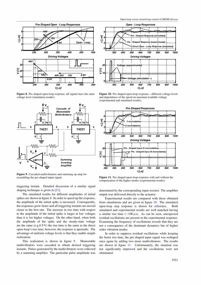
Figure 12. Controller structure [9, 7].
Figure 13. Open- and closed-loop responses and voltagecorresponding to closed-loop response.
4.2. Closed-loop driving
The next step is the implementation of the feedback controller.Optical feedback (9) was used to measure the position as shownin figure 3. The controller contains feed-forward (FF) andfeedback proportional derivative (PD) loop, and is shown infigure 12. The detailed design of the controller is providedin [9]. Realization was accomplished using a fast controlprototyping dSpace system. The sampling time was 12 µs.Under the assumption of perfect position reconstruction, e.g.x = x∗ in (9), the control action is given as
uff = (k/ke)xd
ufb + (1/N)ufb = KP(xd − x) + KD(x)(xd − x)
u = uff + ufb u � 0V = √
uff + ufb 0 � V � 15V
(12)
with KD = 3.2 × 10³ and KP = 3.2 × 10⁷.The feed-forward gain ensures reaching the vicinity of the
desired deflection. Proportional and derivative gains mitigatethe remaining error, speed up the response and shape the signal,ensuring the aperiodic response. Experimental responses ofthe closed-loop system to the step input signal are shownin figure 13. The open-loop response is also shown forcomparison.
The rise time of the closed-loop system is around 170 µs,which is faster than the rise time of the open-loop stepresponse (190 µs). However, it is slower than the rise timeof the pre-shaped case (100 µs). The rise time in the closed-loop case is limited by the minimum achievable samplingtime (12 µs). It is interesting to observe that there areno visible residual oscillations present in the closed-loopresponse. Typically, closed-loop control dramatically reducesthe system’s sensitivity to vibrations [22].
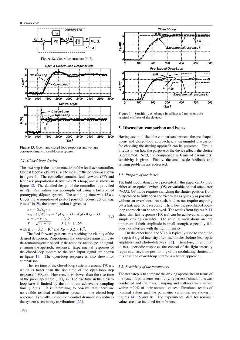
Figure 14. Sensitivity on change in stiffness; k represents theoriginal stiffness of the device.
5. Discussion: comparison and issues
Having accomplished the comparison between the pre-shapedopen- and closed-loop approaches, a meaningful discussionfor choosing the driving approach can be presented. First, adiscussion on how the purpose of the device affects the choiceis presented. Next, the comparison in terms of parameters’sensitivity is given. Finally, the small scale feedback andsensing problems are addressed.
5.1. Purpose of the device
The light modulating device presented in this paper can be usedeither as an optical switch (OS) or variable optical attenuator(VOA). OS mode requires switching the shutter position fromfully closed to fully open and vice versa as quickly as possible,without an overshoot. As such, it does not require anythingbut a fast, aperiodic response. Therefore the pre-shaped open-loop approach can be employed. The results from figures 9–11show that fast response (100 µs) can be achieved with quitesimple driving circuitry. The residual oscillations are notimportant if their amplitude is small enough, especially if itdoes not interfere with the light intensity.
On the other hand, the VOA is typically used to conditionthe optical signal intensity after laser diodes, before fiber-opticamplifiers and photo-detectors [15]. Therefore, in additionto fast, aperiodic response, the control of the light intensityrequires an accurate positioning of the modulating shutter. Inthis case, the closed-loop control is a better approach.
5.2. Sensitivity of the parameters
The next step is to compare the driving approaches in terms ofthe system’s parameter sensitivity. A series of simulations wasconducted and the mass, damping and stiffness were variedwithin ±20% of their nominal values. Simulated results ofnominal values and the parameter variations are shown infigures 14, 15 and 16. The experimental data for nominalvalues are also included for reference.
1922

Open-loop versus closed-loop control of MEMS devices
Figure 15. Sensitivity on change in damping; d represents theoriginal damping of the device.
Figure 16. Sensitivity on change in mass; m represents the originalmass of the device.
It is obvious that the closed-loop driving renders muchless sensitivity to the parameter changes.
5.3. Problems—small scale feedback
Contemporary macro-scale control systems are typicallyimplemented with micro-controllers that execute a digitalcontrol algorithm. Sensors are relatively small in comparisonto the controlled system and are quite easily implementedanywhere they need to be. Several factors make MEMS controlsystems unique. First, unlike macro systems, MEMS systemsare small and typically very fast. Second, the implementationof the sensor on the device can significantly change the sizeand dynamics of the device. Third, the whole control systemshould be integrated with the MEMS device and thereforeshould be as small as possible.
Response times of MEMS range from a few ms for largeDRIE fabricated thermal actuators to µs ranges for small
Figure 17. Difference between capacitive and optical sensing.
surface electrostatic devices [18]. Conversion times for thestandard D/A and A/D converters range from 1 to 10 µs. Thisexcludes the application of the micro-controller for devicesfaster than 100 µs. The use of a micro-controller becomesquestionable not only because of conversion times, but becauseit is too large to be integrated with MEMS devices. Due to theimplementation size, the control algorithm should be kept assimple as possible. Control algorithms can be implementedas digital filters with sequential stages of multiplication andaccumulation [22], or they can be implemented using analogtechniques [7].
Position sensing makes the control system even morecomplicated. There are several ways to sense position. For theMEMS device described in this paper we implemented opticalsensing, which, as a sensing approach, has several problems.First, the relationship between the actual position of the deviceand the output optical intensity is nonlinear. Moreover, smallfiber misalignments can cause relatively large errors in thesensor output. The shape of the optical cavity enclosingthe sensing point (figure 6) can significantly influence thequality of the measurement (figure 7), especially if the cavity’sdimensions are comparable to the wavelength (1.5 µm) of thelight used. An unstable light source can also influence themeasurement significantly.
Capacitive sensors are typically implemented as adifferential capacitance [22]. As is shown in figure 17, thesensor becomes a part of the device. Electronic circuitry,converting the capacitance to a voltage and position, is attachedto the sensor. A number of signal processing techniqueshave been developed [18, 19, 22, 23] to extract the positionfrom the measured capacitance. It is favorable to have aslarge a capacitance as possible to get high resolution and highsignal-to-noise ratio (SNR) [22]; however, the larger capacitorrequires larger area which consequently increases the massof the device slowing its response. Practically, however, theachievable values of microcapacitors are typically in the fF–pFrange, and therefore interfere with the value of the parasiticcapacitance of the attached electronics (a few pF) [22]. Inorder to mitigate the effects of these shunt capacitances it isdesirable to integrate IC and MEMS devices together [22].
6. Conclusions
As a result of the analysis and experiments conducted for bothopen- and closed-loop control of MEMS, some conclusionsregarding the performance of different control approaches canbe drawn.
1923
B Borovic et al
In terms of the complexity for the driving and sensingelectronics, an open-loop approach has advantages overclosed-loop control as it uses only driving circuits. Onthe other hand, open-loop driving is sensitive to parameteruncertainties and the shape of the input signal. The inputvoltage spikes have to be timed very precisely. For studieddevice the accuracy of the triggering time is typically lessthan 0.1 µs. Faster responses and higher voltages requireeven higher precision. The closed-loop control approach issignificantly less sensitive to changes in system parameters,and generates oscillation-free response [22]. Sometimes, as inthe case of charge (current) driving of the electrostatic device,it is necessary to implement position feedback. Leakagesthrough parallel parasitic capacitances make it very hard tokeep the charge on the actuator.
In terms of application requirements, when a MEMSdevice is used for switching, only two signal levels are ofinterest and the best way to drive it is using pre-shaped open-loop signals. However, if the actuator has to be accuratelypositioned between 0 and 100%, as in the case of VOA, it ismore suitable to use a closed-loop approach.
In conclusion, the choice of the control systems for MEMSdepends on the available sensor, and the size and the speed ofthe device. The most difficult aspect of implementation isrelated to the hardware necessary for control, rather than thecontrol algorithms. Finally, the control algorithms should bekept as simple as possible so they can be integrated directly inhardware with IC and optical components.
Acknowledgment
This work is supported by ARO grant DAAD19-02-1-0366and NSF GOALI BES 0201773.
References
[1] Bryzek J, Abbott E, Flannery A, Cagle D and Maitan J 2003Control issues for MEMS Proc. Conf. Decision and Control2004 (Nassau, Bahamas, Dec. 14–17)
[2] Jensen B D, Mutlu S, Miller S, Kurabayashi K and Allen J J2003 Shaped comb fingers for tailored electromechanicalrestoring force, J. Microelectromech. Syst. 12 373–83
[3] Chen C and Lee C 2004 Design and modeling for comb driveactuator with enlarged static displacement SensorsActuators A 115 530–9
[4] Grade J D, Jerman H and Kenny T W 2003 Design of largedeflection electrostatic actuators J. Microelectromech. Syst.12 335–43
[5] Popa D O, Wen J T, Stephanou H E, Skidmore G and Ellis M2004 Dynamic modeling and input shaping for MEMSTechnical Proc. 2004 NSTI Nanotechnology Conf. andTrade Show (NANOTECH 2004) (Boston, MA, 7–11 March)vol 2 pp 315–8
[6] Popa D O, Kang B H, Wen J T, Stephanou H E, Skidmore Gand Geisberger A 2003 Dynamic modeling and inputshaping of thermal bimorph actuators Proc. 2003 IEEE Int.Conf. on Robotics Automation (Taipei, Taiwan, 14–19 Sept.)
[7] Borovic B, Hong C, Zhang X M, Liu A Q and Lewis F L2005 Open vs. closed-loop control of the MEMSelectrostatic comb drive 13th Mediterranean Conf. onControl and Automation, MED 2005 (Limassol, Cyprus,27–29 May)
[8] Lu M S-C and Fedder G K 2004 Position control ofparallel-plate microactuators for probe-based data storageJ. Microelectromech. Syst. 13 759–69
[9] Borovic B, Hong C, Liu A Q, Xie L and Lewis F L 2004Control of a MEMS optical switch Int. Conf. Decision andControl, CDC 2004 (Nassau, Bahamas, 14–17 Dec.)
[10] Sun Y, Nelson B J, Potasek D P and Enikov E 2002 A bulkmicrofabricated multi-axis capacitive cellular force sensorusing transverse comb drives J. Micromech. Microeng. 12832–40
[11] Sun Y, Piyabongkarn D, Sezen A, Nelson B J and Rajamani R2002 A high-aspect-ratio two-axis electrostaticmicroactuator with extended travel range Sensors ActuatorsA 102 49–60
[12] Tang W C, Nguyen T H and Howe R T 1989 Laterally drivenpolysilicon resonant microstructures Sensors Actuators 2025–32
[13] Liu A Q, Zhang X M, Lu C, Wang F, Lu C and Liu Z S 2003Optical and mechanical models for a variable opticalattenuator using a micromirror drawbridge J. Micromech.Microeng. 13 400–11
[14] Li J, Zhang Q X and Liu A Q 2003 Advanced fiber opticalswitches using deep RIE (DRIE) fabrication SensorsActuators A 102 286–95
[15] Isamoto K, Kato K, Morosawa A, Chong C, Fujita H andToshiyoshi H 2004 A 5-V operated MEMS variable opticalattenuator by SOI bulk micromachining IEEE J. Sel. Top.Quantum Electron. 10 570–8
[16] Klaasen E, Petersen K, Noworolski J, Logan J, Maluf N,Brown J, Storment C, McCulley W and Kovacs G 1996Silicon fusion bonding and deep reactive ion etching:a new technology for microstructures Sensors Actuators A52 132–9
[17] Fujita H 1998 Microactuators and micromachines Proc. IEEE86 1721–32
[18] Senturia S D 2000 Microsystem Design (Dordrecht: Kluwer)[19] Elswenpoek M and Wiegerink R 2001 Mechanical
Microsensors (Berlin: Springer)[20] Borovic B, Liu A Q, Popa D, Xuming Z and Lewis F L
2005 Lateral motion control of electrostatic comb drive:new methods in modeling and sensing Proc. 16thIASTED Int. Conf. Modeling and Simulation (18–20 May)pp 301–7
[21] Lewis F L, Dawson D M, Lin J and Liu K 1991 TankGun-Pointing Control with Barrel Flexibility Effects(Atlanta: ASME, WAM)
[22] Bryzek J, Flannery A and Skurnik D 2004 Integratingmicroelectromechanical systems with integrated circuitsIEEE Instrum. Meas. Mag. 7 51–9
[23] Seeger J I and Boser B B 2003 Charge control ofparallel-plate, electrostatic actuators and the tip-ininstability J. Microelectromech. Syst. 12 656–71
1924