Embed Size (px)
Citation preview

I. The New Perspective
All Rights Reserved
15
I. The New Perspective
Chapter 2. (L1.2 - L1.3, L1.9) Why Electrons Flow 17 Chapter 3. (L1.4) The Elastic Resistor 31 Chapter 4. (L1.5 - L1.7) Ballistic and Diffusive Transport 41 Chapter 5.* NOT covered in this course Kubo Formula 49 Appendix A: (L1.4) Fermi and Bose Function Derivatives 57 Appendix B: (L1.8) Angular Averaging 59 Further Reading 61
Lessons from Nanoelectronics
Copyright Supriyo Datta
16
Why Electrons Flow
All Rights Reserved
17
Chapter 2
Why Electrons Flow
2.1. Two Key Concepts 2.2. Fermi Function 2.3. Non-equilibrium: Two Fermi Functions 2.4. Linear Response 2.5. Difference in “Agenda” Drives the Flow 2.6. Degenerate and Non-degenerate Conductors It is a well-known and well-established fact, namely that when the two terminals of a battery are connected across a conductor, it gives rise to a current due to the flow of electrons across the channel from the source to the drain. If you ask anyone, novice or expert, what causes electrons to flow, by far the most common answer you will receive is that it is the electric field. However, this answer is incomplete at best. After all even before we connect a battery, there are enormous electric fields around every atom due to the positive nucleus whose effects on the atomic spectra are well-documented. Why is it that these electric fields do not cause electrons to flow, and yet a far smaller field from an external battery does? The standard answer is that microscopic fields do not cause current to flow, a macroscopic field is needed. This too is not satisfactory, for two reasons. Firstly, there are well-known inhomogeneous conductors like p-n junctions which have large macroscopic fields extending over many micrometers that do not cause any flow of electrons till an external battery is connected.

Lessons from Nanoelectronics
Copyright Supriyo Datta
18
Secondly, experimentalists are now measuring current flow through conductors that are only a few atoms long with no clear distinction between the microscopic and the macroscopic. This is a result of our progress in nanoelectronics, and it forces us to search for a better answer to the question, “why electrons flow.”
2.1 Two Key Concepts
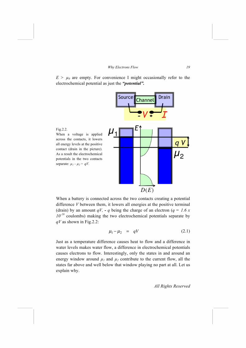
To answer this question, we need two key concepts. First is the density of states per unit energy D(E) available for electrons to occupy inside the channel (Fig.2.1). For the benefit of experts, I should note that we are adopting what we will call a "point channel model" represented by a single density of states D(E). More generally one needs to consider the spatial variation of D(E), as we will see in Chapter 7, but there is much that can be understood just from our point channel model. Fig.2.1. The first step in understanding the operation of any electronic device is to draw the available density of states D(E) as a function of energy E, inside the channel and to locate the equilibrium electrochemical potential µ0 separating the filled from the empty states.
The second key input is the location of the electrochemical potential, µ0 which at equilibrium is the same everywhere, in the source, the drain and the channel. Roughly speaking (we will make this statement more precise shortly) it is the energy that demarcates the filled states from the empty ones. All states with energy E < µ0 are filled while all states with
Why Electrons Flow
All Rights Reserved
19
E > µ0 are empty. For convenience I might occasionally refer to the electrochemical potential as just the “potential”. Fig.2.2. When a voltage is applied across the contacts, it lowers all energy levels at the positive contact (drain in the picture). As a result the electrochemical potentials in the two contacts separate: µ1 - µ2 = qV.
When a battery is connected across the two contacts creating a potential difference V between them, it lowers all energies at the positive terminal (drain) by an amount qV, - q being the charge of an electron (q = 1.6 x 10⁻¹⁹ coulombs) making the two electrochemical potentials separate by qV as shown in Fig.2.2:
(2.1)
Just as a temperature difference causes heat to flow and a difference in water levels makes water flow, a difference in electrochemical potentials causes electrons to flow. Interestingly, only the states in and around an energy window around µ1 and µ2 contribute to the current flow, all the states far above and well below that window playing no part at all. Let us explain why.
µ1 − µ2 = qV

Lessons from Nanoelectronics
Copyright Supriyo Datta
20
2.1.1 Energy Window for Current Flow
Each contact seeks to bring the channel into equilibrium with itself, which roughly means filling up all the states with energies E less than its electrochemical potential µ and emptying all states with energies greater than µ. Consider the states with energy E that are less than µ1 but greater than µ2. Contact 1 wants to fill them up since E < µ1, but contact 2 wants to empty them since E > µ2. And so contact 1 keeps filling them up and contact 2 keeps emptying them causing electrons to flow continually from contact 1 to contact 2. Consider now the states with E greater than both µ1 and µ2. Both contacts want these states to remain empty and they simply remain empty with no flow of electrons. Similarly the states with E less than both µ1 and µ2 do not cause any flow either. Both contacts like to keep them filled and they just remain filled. There is no flow of electrons outside the window between µ1 and µ2, or more correctly outside ± a few kT of this window, as we will discuss shortly. This last point may seem obvious, but often causes much debate because of the common belief we alluded to earlier, namely that electron flow is caused by the electric field in the channel. If that were true, all the electrons should flow and not just the ones in any specific window determined by the contacts.
2.2 Fermi Function
Let us now make the above statements more precise. We stated that roughly speaking, at equilibrium, all states with energies E below the electrochemical potential µ are filled while all states with E > µ are empty. This is precisely true only at absolute zero temperature. More generally, the transition from completely full to completely empty occurs over an energy range ~ ± 2 kT around E = µ where k is the Boltzmann

Why Electrons Flow
All Rights Reserved
21
constant (~ 80 µeV/K) and T is the absolute temperature. Mathematically this transition is described by the Fermi function :
(2.2)
This function is plotted in Fig.2.3 (left panel), though in an unconventional form with the energy axis vertical rather than horizontal. This will allow us to place it alongside the density of states, when trying to understand current flow (see Fig.2.4). Fig.2.3. Fermi function and the normalized (dimensionless) thermal broadening function. For readers unfamiliar with the Fermi function, let me note that an extended discussion is needed to do justice to this deep but standard result, and we will discuss it a little further in Lecture 16 when we talk about the key principles of equilibrium statistical mechanics. At this stage it may help to note that what this function (Fig.2.3) basically tells us is that states with low energies are always occupied (f=1), while states with high energies are are always empty (f=0), something that seems reasonable since we have heard often enough that (1) everything goes to its lowest energy, and (2) electrons obey an exclusion principle that stops
f (E) =1
expE − µ
kT
⎛⎝⎜
⎞⎠⎟+ 1

Lessons from Nanoelectronics
Copyright Supriyo Datta
22
them from all getting into the same state. The additional fact that the Fermi function tells us is that the transition from f=1 to f=0 occurs over an energy range of ~ ± 2kT around µ0.
2.2.1. Thermal Broadening Function
Also shown in Fig.2.3 is the derivative of the Fermi function, multiplied by kT to make it dimensionless:
(2.3a)
Using Eq.(2.2) it is straightforward to show that
(2.3b)
Note:
(1) From Eq.(2.3b) it can be seen that
(2.4a)
(2) From Eqs.(2.3b) and (2.2) it can be seen that
(2.4b)
(3) If we integrate FT over all energy the total area equals kT:
(2.4c)
so that we can approximately visualize FT as a rectangular "pulse" centered around E=µ with a peak value of 1/4 and a width of ~ 4kT.
FT (E,µ) = kT −∂ f∂E
⎛⎝⎜
⎞⎠⎟
FT (E,µ) =ex
(ex+1)
2, where x ≡
E − µ
kT
FT(E,µ) = F
T(E − µ) = F
T(µ − E)
FT = f (1− f )
dE
− ∞
+ ∞
∫ FT (E,µ) = kT dE
− ∞
+ ∞
∫ −∂ f∂E
⎛⎝⎜
⎞⎠⎟
= kT − f[ ]−∞
+∞= kT (1− 0) = kT

Why Electrons Flow
All Rights Reserved
23
2.3 Non-equilibrium: Two Fermi Functions
When a system is in equilibrium the electrons are distributed among the available states according to the Fermi function. But when a system is driven out-of-equilibrium there is no simple rule for determining the distribution of electrons. It depends on the specific problem at hand making non-equilibrium statistical mechanics far richer and less understood than its equilibrium counterpart. For our specific non-equilibrium problem, we argue that the two contacts are such large systems that they cannot be driven out-of-equilibrium. And so each remains locally in equilibrium with its own electrochemical potential giving rise to two different Fermi functions (Fig.2.4):
(2.5a)
(2.5b)
The "little" channel in between does not quite know which Fermi function to follow and as we discussed earlier, the source keeps filling it up while the drain keeps emptying it, resulting in a continuous flow of current.
In summary, what makes electrons flow is the difference in the "agenda" of the two contacts as reflected in their respective Fermi functions, f1(E) and f2(E). This is qualitatively true for all conductors, short or long. But for short conductors, the current at any given energy E is quantitatively proportional to
representing the difference in the probabilities in the two contacts. This quantity goes to zero when E lies way above µ1, µ2 since f1 and f2 are
f1(E) =1
expE − µ1kT
⎛⎝⎜
⎞⎠⎟+ 1
f2(E) =1
expE − µ2kT
⎛⎝⎜
⎞⎠⎟+ 1
€
I(E) ~ f1(E) − f2(E)

Lessons from Nanoelectronics
Copyright Supriyo Datta
24
both zero. It also goes to zero when E lies way below µ1, µ2 since f1 and f2 are both one. Current flow occurs only in the intermediate energy window, as we had argued earlier.
Fig.2.4. Electrons in the contacts occupy the available states with a probability described by a Fermi function f(E) with the appropriate electrochemical potential µ.
2.4 Linear Response
Current-voltage relations are typically not linear, but there is a common approximation that we will frequently use throughout these lectures to extract the "linear response" which refers to the low bias conductance, dI/ dV, as V 0.
The basic idea can be appreciated by plotting the difference between two Fermi functions, normalized to the applied voltage
(2.6)
where
F(E) =f1(E)− f2(E)
qV / kT
µ1 = µ0 + (qV / 2)
µ2 = µ0 − (qV / 2)

Why Electrons Flow
All Rights Reserved
25
Fig.2.5 shows that the difference function F gets narrower as the voltage is reduced relative to kT. The interesting point is that as qV is reduced below kT, the function F approaches the thermal broadening function FT we defined (see Eq.(2.3a)) in Section 2.2:
so that from Eq.(2.6)
(2.7)
if the applied voltage µ1 - µ2 = qV is much less than kT.
Fig.2.5. F(E) from Eq.(2.6) versus (E-µ0)/kT for different values of y=qV/kT.
The validity of Eq.(2.7) for qV << kT can be checked numerically if you have access to MATLAB or equivalent. For those who like to see a mathematical derivation, Eq.(2.7) can be obtained using the Taylor series expansion described in Appendix A to write
f (E)− f0(E) ≈ −∂ f0∂E
⎛⎝⎜
⎞⎠⎟(µ − µ0 ) (2.8)
Eq.(2.8) and Eq.(2.7) which follows from it, will be used frequently in these lectures.
F(E) → FT (E), as qV / kT → 0
f1(E)− f2(E) ≈qV
kTFT (E,µ0 ) = −
∂ f0∂E
⎛⎝⎜
⎞⎠⎟qV

Lessons from Nanoelectronics
Copyright Supriyo Datta
26
2.5. Difference in “Agenda” Drives the Flow
Before moving on, let me quickly reiterate the key point we are trying to make, namely that current is determined by
−∂ f0(E)
∂Eand not by f0(E)
The two functions look similar over a limited range of energies
−∂ f0(E)
∂E≈
f0(E)
kTif E − µ0 >> kT
So if we are dealing with a so-called “non-degenerate conductor” where we can restrict our attention to a range of energies satisfying this criterion, we may not notice the difference.
But in general these functions look very different (see Fig.2.3) and the experts agree that current depends not on the Fermi function, but on its derivative. However, we are not aware of any elementary treatment that leads to this result.
Freshman physics texts start by treating the force due to an electric electric field F as the driving term and adding a frictional term to Newton’s law (τ
mis the so-called “momentum relaxation time”)
d(mv)
dt= (−qF)
Newton 's Law
−mv
τm
Friction
At steady-state (d/dt = 0) this gives a non-zero drift velocity,
νd = − qτmm
mobility
F
from which one calculates the current. This elementary approach leads to the Drude formula, stated earlier in Eq.(1.5b)), which played a major historical role in our understanding of current flow.

Why Electrons Flow
All Rights Reserved
27
Since the above approach treats electric fields as the driving term, it also suggests that the current depends on the total number of electrons. This is commonly explained away by saying that there are mysterious quantum mechanical forces that prevent electrons in full bands from moving and what matters is the number of “free electrons”. But this begs the question of which electrons are free and which are not, a question that becomes more confusing for atomic scale conductors.
It is well-known that the conductivity varies widely, changing by a factor of ~1020 going from copper to glass, to mention two materials that are near two ends of the spectrum. But this is not because one has more electrons than the other. The total number of electrons is of the same order of magnitude for all materials from copper to glass.
Whether a conductor is good or bad is determined by the availability of states in an energy window ~ kT around the electrochemical potential µ0, which can vary widely from one material to another. This is well-known to experts and comes mathematically from the dependence of the conductivity
on −∂ f0(E)
∂Erather than f0(E)
a result that typically requires advanced treatments based on the Boltzmann (Lecture 7) or the Kubo formalism (Lecture 15).
Our bottom-up approach, however, leads us to this result in an elementary way as we have just seen. Current is driven by the difference in the “agenda” of the two contacts which for low bias is proportional to the derivative of the equilibrium Fermi function:
f1(E)− f2(E) ≈ −∂ f0∂E
⎛⎝⎜
⎞⎠⎟qV
There is no need to invoke mysterious forces that stops some electrons from moving, though one could perhaps call f1 - f2 a mysterious force, since the Fermi function (Eq.(2.2)) reflects the exclusion principle.
Lessons from Nanoelectronics
Copyright Supriyo Datta
28
Later when we (briefly) discuss phonon transport, we will see how this approach is readily extended to describe the flow of phonons which is proportional to n1 – n2 , n being the Bose (not Fermi) function which is appropriate for particles that do not have an exclusion principle.
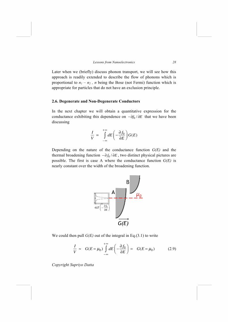
2.6. Degenerate and Non-Degenerate Conductors
In the next chapter we will obtain a quantitative expression for the conductance exhibiting this dependence on −∂f0 / ∂E that we have been discussing
I
V= dE −
∂ f0∂E
⎛⎝⎜
⎞⎠⎟
−∞
+∞
∫ G(E)
Depending on the nature of the conductance function G(E) and the thermal broadening function −∂ f0 / ∂E , two distinct physical pictures are possible. The first is case A where the conductance function G(E) is nearly constant over the width of the broadening function. We could then pull G(E) out of the integral in Eq.(3.1) to write
I
V≈ G(E = µ0 ) dE −
∂ f0∂E
⎛⎝⎜
⎞⎠⎟
−∞
+∞
∫ = G(E = µ0 ) (2.9)

Why Electrons Flow
All Rights Reserved
29
This relation suggests an operational definition for the conductance function G(E): It is the conductance measured at low temperatures for a channel with its electrochemical potential µ0 located at E. The actual conductance is obtained by averaging G(E) over a range of energies using −∂ f0 / ∂E as a “weighting function”. Case A is a good example of the so-called degenerate conductors. The other extreme is the non-degenerate conductor shown in case B where the electrochemical potential is located at an energy many kT’s below the energy range where the conductance function is non-zero. As a result over the energy range of interest where G(E) is non-zero, we have
x ≡E − µ0
kT>> 1
and it is common to approximate the Fermi function with the Boltzmann function
1
1+ ex
≈ e−x
so that I
V≈
dE
kT−∞
+∞
∫ G(E) e−(E−µ
0)/kT
This non-degenerate limit is commonly used in the semiconductor literature though the actual situation is often intermediate between degenerate and non-degenerate limits.

Lessons from Nanoelectronics
Copyright Supriyo Datta
30

The Elastic Resistor
All Rights Reserved
31
Chapter 3
The Elastic Resistor
3.1. How an Elastic Resistor Dissipates Heat 3.2. Conductance of an Elastic Resistor 3.3. Why an Elastic Resistor is Relevant
We saw in the last Lecture that the flow of electrons is driven by the difference in the "agenda" of the two contacts as reflected in their respective Fermi functions, f1(E) and f2(E). The negative contact with its larger f(E) would like to see more electrons in the channel than the positive contact. And so the positive contact keeps withdrawing electrons from the channel while the negative contact keeps pushing them in.
This is true of all conductors, big and small. But it is generally difficult to express the current as a simple function of f1(E) and f2(E), because electrons jump around from one energy to another and the current flow at different energies is all mixed up.
Fig.3.1. An elastic resistor: Electrons travel along fixed energy channels. But for the ideal elastic resistor shown in Fig.1.4, the current in an energy range from E to E+dE is decoupled from that in any other energy range, allowing us to write it in the form (Fig.3.1)
dI =1
qdE G(E) ( f1(E)− f2(E))
Lessons from Nanoelectronics
Copyright Supriyo Datta
32
and integrating it to obtain the total current I. Making use of Eq.(2.7), this leads to an expression for the low bias conductance
I
V= dE −
∂ f0∂E
⎛⎝⎜
⎞⎠⎟
−∞
+∞
∫ G(E) (3.1)
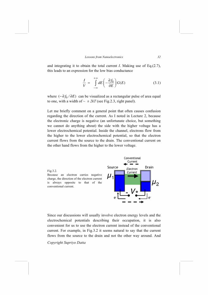
where can be visualized as a rectangular pulse of area equal to one, with a width of ~ ± 2kT (see Fig.2.3, right panel). Let me briefly comment on a general point that often causes confusion regarding the direction of the current. As I noted in Lecture 2, because the electronic charge is negative (an unfortunate choice, but something we cannot do anything about) the side with the higher voltage has a lower electrochemical potential. Inside the channel, electrons flow from the higher to the lower electrochemical potential, so that the electron current flows from the source to the drain. The conventional current on the other hand flows from the higher to the lower voltage. Fig.3.2. Because an electron carries negative charge, the direction of the electron current is always opposite to that of the conventional current. Since our discussions will usually involve electron energy levels and the electrochemical potentials describing their occupation, it is also convenient for us to use the electron current instead of the conventional current. For example, in Fig.3.2 it seems natural to say that the current flows from the source to the drain and not the other way around. And
(−∂ f0 / ∂E)
The Elastic Resistor
All Rights Reserved
33
that is what I will try to do consistently throughout these Lectures. In short, we will use the current, I, to mean electron current. Getting back to Eq.(3.1), we note that it tells us that for an elastic resistor, we can define a conductance function G(E) whose average over an energy range ~ ± 2kT around the electrochemical potential µ0 gives the experimentally measured conductance. At low temperatures, we can simply use the value of G(E) at E = µ0.
This energy-resolved view of conductance represents an enormous simplification that is made possible by the concept of an elastic resistor which is a very useful idealization that describes short devices very well and provides insights into the operation of long devices as well.
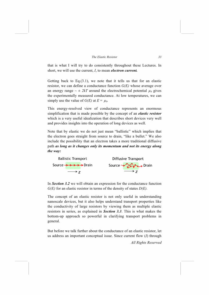
Note that by elastic we do not just mean “ballistic” which implies that the electron goes straight from source to drain, “like a bullet.” We also include the possibility that an electron takes a more traditional diffusive path as long as it changes only its momentum and not its energy along the way:
In Section 3.2 we will obtain an expression for the conductance function G(E) for an elastic resistor in terms of the density of states D(E).
The concept of an elastic resistor is not only useful in understanding nanoscale devices, but it also helps understand transport properties like the conductivity of large resistors by viewing them as multiple elastic resistors in series, as explained in Section 3.3. This is what makes the bottom-up approach so powerful in clarifying transport problems in general. But before we talk further about the conductance of an elastic resistor, let us address an important conceptual issue. Since current flow (I) through

Lessons from Nanoelectronics
Copyright Supriyo Datta
34
a resistor (R) dissipates a Joule heat of I2R per second, it seems like a contradiction to talk of an elastic resistor where electrons do not lose energy? The point to note is that while the electron does not lose any energy in the channel of an elastic resistor, it does lose energy both in the source and the drain and that is where the Joule heat gets dissipated. This is a very non-intuitive result that seems to be at least approximately true of nanoscale conductors: An elastic resistor has a resistance R determined by the channel, but the corresponding heat I2R is entirely dissipated outside the channel.
3.1. How an Elastic Resistor Dissipates Heat
How could this happen? Consider a one level elastic resistor having one sharp level with energy ε . Every time an electron crosses over through the channel, it appears as a "hot electron" on the drain side with an energy ε in excess of the local electrochemical potential µ2 as shown below:
Energy dissipating processes in the contact quickly make the electron get rid of the excess energy ( ε − µ2 ). Similarly at the source end an empty spot (a "hole") is left behind with an energy that is much less than the local electrochemical potential µ1, which gets quickly filled up by electrons dissipating the excess energy ( µ1 − ε ).
In effect, every time an electron crosses over from the source to the drain,
€
ε

The Elastic Resistor
All Rights Reserved
35
The total energy dissipated is
which is supplied by the external battery that maintains the potential difference µ1 - µ2. The overall flow of electrons and heat is summarized in Fig.3.3 below.
Fig.3.3. Flow of electrons and heat in a one-level elastic resistor having one level with E = ε .
If N electrons cross over in a time t
since
Note that V*I is the same as I2R and V2G. The heat dissipated by an "elastic resistor" thus occurs in the contacts. As we will see next, the detailed mechanism underlying the complicated process of heat transfer in the contacts can be completely bypassed simply by legislating that the contacts are always maintained in equilibrium with a fixed electrochemical potential.
an energy (µ1 − ε ) is dissipated in the source
an energy (ε − µ2 ) is dissipated in the drain
µ1 − µ2 = qV
Dissipated power = qV *N / t = V * I
Current = q*N / t

Lessons from Nanoelectronics
Copyright Supriyo Datta
36
3.2. Conductance of an Elastic Resistor
Consider first the simplest elastic resistor having just one level with energy in the energy range of interest through which electrons can squeeze through from the source to the drain. We can write the resulting current as
(3.2)
where t is the time it takes for an electron to transfer from the source to the drain. We can extend Eq.(3.2) for the current through a one-level resistor to any elastic conductor (Fig.3.1) with an arbitrary density of states D(E), noting that all energy channels conduct independently in parallel. We could first write the current in an energy channel between E and E+dE
dI = dED(E)
2
q
t( f1(E)− f2(E))
since an energy channel between E and E+dE contains D(E)dE states, half of which contribute to carrying current from source to drain.
Integrating we obtain an expression for the current through an elastic resistor:
I =1
q− ∞
+ ∞
∫ dE G(E) ( f1(E)− f2(E)) (3.3)
where (3.4)
If the applied voltage µ1 - µ2 = qV is much less than kT, we can use Eq.(2.7) to write
€
ε
€
Ione level =q
tf1(ε) − f2(ε)( )
G(E) =q2D(E)
2t(E)

The Elastic Resistor
All Rights Reserved
37
which yields the expression for conductance stated earlier in Eq.(3.1).
As we discussed in Section 2.6, if the conductance function G(E) is nearly constant over the width of the broadening function, we could pull G(E) out of the integral in Eq.(3.1) to write
I
V≈ G(E = µ0 ) dE −
∂ f0∂E
⎛⎝⎜
⎞⎠⎟
−∞
+∞
∫ = G(E = µ0 ) (3.5)
suggesting an operational definition for the conductance function G(E): It is the conductance measured at low temperatures for a channel with its electrochemical potential µ0 located at E. We will generally use the degenerate limit expressed by Eq.(3.5) writing
with the understanding that the quantities D and t are evaluated at E = µ0 and depending on the nature of G(E) may need to be averaged over a range of energies using −∂ f0 / ∂E as a “weighting function” as prescribed by Eq.(3.1). Eq.(3.4) seems quite intuitive: it says that the conductance is proportional to the product of two factors, namely the availability of states (D) and the ease with which electrons can transport through them (1/t). This is the key result that we will use in subsequent chapters.
3.3. Why an Elastic Resistor is Relevant
The elastic resistor model is clearly of great value in understanding nanoscale conductors, but the reader may well wonder how an elastic
I = V dE
− ∞
+ ∞
∫ −∂ f0∂E
⎛⎝⎜
⎞⎠⎟G(E)
G =q2D
2t

Lessons from Nanoelectronics
Copyright Supriyo Datta
38
resistor can capture the physics of real conductors which are surely far from elastic? In long conductors inelastic processes are distributed continuously through the channel, inextricably mixed up with all the elastic processes (Fig.3.4). Doesn't that affect the conductance and other properties we are discussing?
Fig.3.4 Real conductors have inelastic scatterers distributed throughout the channel.
Fig.3.5 A hypothetical series of elastic resistors as an approximation to a real resistor with distributed inelastic scattering as shown in Fig.3.4.
One way to apply the elastic resistor model to a large conductor with distributed inelastic processes is to break up the latter conceptually into a sequence of elastic resistors (Fig.3.5), each much shorter than the physical length L, having a voltage that is only a fraction of the total voltage V. We could then argue that the total resistance is the sum of the individual resistances.

The Elastic Resistor
All Rights Reserved
39
This splitting of a long resistor into little sections of length shorter than Lin (Lin: length an electron travels on the average before getting inelastically scattered) also helps answer another question one may raise about the elastic resistor model. We obtained the linear conductance by resorting to a Taylor’s series expansion (see Eq.(2.6)). But keeping the first term in the Taylor’s series can be justified only for voltages V < kT/q, which at room temperature equals 25 mV. But everyday resistors are linear for voltages that are much larger. How do we explain that? The answer is that the elastic resistor model should only be applied to a short length < Lin and as long as the voltage dropped over a length Lin is less than kT/q we expect the current to be linear with voltage. The terminal voltage can be much larger.
However, this splitting into short resistors needs to be done carefully. A key result we will discuss in the next Lecture is that Ohm’s law should be modified
from R = ρAL
Eq.(1.1)
to R = ρA
L + λ( )Eq.(1.4)
to include an extra fixed resistance that is independent of the length and can be viewed as an interface resistance associated with the channel- contact interfaces. Here is a length of the order of a mean free path, so that this modification is primarily important for near ballistic conductors (L ~ ) and is negligible for conductors that are many mean free paths long (L >> ).
Conceptually, however, this additional resistance is very important if we wish to use the hypothetical structure in Fig.3.5 to understand the real structure in Fig.3.4. The structure in Fig.3.5 has too many interfaces that are not present in the real structure of Fig.3.4 and we have to remember to exclude the resistance coming from these conceptual interfaces.
For example, if each section in Fig.3.5 is of length L having a resistance of
ρλ / A
λ
λ
λ

Lessons from Nanoelectronics
Copyright Supriyo Datta
40
then the correct resistance of the real structure in Fig.3.4 of length 3L is given by
Clearly we have to be careful to separate the interface resistance from the length dependent part. This is what we will do next.
R =ρ(L + λ)
A
R =ρ(3L + λ)
Aand NOT by R =
ρ(3L + 3λ)
A

Ballistic and Diffusive Transport
All Rights Reserved
41
Chapter 4
Ballistic and Diffusive Transport
4.1. Ballistic and Diffusive Transfer Times 4.2. Channels for Conduction
We saw in the last Lecture that the resistance of an elastic resistor can be written as
(see Eq.(3.4))
In this Lecture I will first argue that the transfer time t across a resistor of length L for diffusive transport with a mean free path can be related to the time tB for ballistic transport by the relation (Section 4.1)
(4.1)
Combining with Eq.(3.4) we obtain
(4.2)
where (4.3)
We could invert Eq.(4.2) to write the new Ohm’s law
G =σ A
L + λ (4.4a)
G =q2D
2t
λ
t = tB1 +
L
λ
G =GBλ
L + λ
GB ≡q2D
2tB

Lessons from Nanoelectronics
Copyright Supriyo Datta
42
where σ A = GBλ
So far we have only talked about three dimensional resistors with a large cross-sectional area A. Many experiments involve two-dimensional resistors whose cross-section is effectively one-dimensional with a width W, so that the appropriate equations have the form
G =σW
L + λ (4.4b)
where σW = GBλ
Fig.4.1. 3-D, 2-D and 1-D conductors
Finally we have one-dimensional conductors for which
G =σ
L + λ (4.4c)
where σ = GBλ
We could collect all these results and write them compactly in the form

Ballistic and Diffusive Transport
All Rights Reserved
43
G =σ
L + λ1, W , A{ } (4.5)
with σ = GBλ 1,1
W,1
A
⎧⎨⎩
⎫⎬⎭
(4.6)
where the three items in parenthesis correspond to 1-D, 2-D and 3-D conductors. Note that the conductivity has different dimensions in 1-D, 2-D and 3-D, while both GB and have the same dimensions, namely Siemens (S) and meters (m) respectively. The standard Ohm’s law predicts that the resistance will approach zero as the length L is reduced to zero. Of course no one expects it to become zero, but the common belief is that it will approach a value determined by the interface resistance which can be made arbitrarily small with improved contacting technology. What is now well established experimentally is that even with the best possible contacts, there is a minimum interface resistance determined by the properties of the channel, independent of the contact. The modified Ohm's law in Eq.(4.5) reflects this fact: Even a channel of zero length with perfect contacts has a resistance equal to that of a hypothetical channel of length .
But what does it mean to talk about the mean free path of a channel of zero length? The answer is that neither nor mean anything for a short conductor, but their product does. The ballistic resistance has a simple meaning that has become clear in the light of modern experiments as we will see in Section 4.2. It is inversely proportional to the number of channels, M(E) available for conduction, which is proportional to, but not the same as, the density of states, D(E).
The concept of density of states has been with us since the earliest days of solid state physics. By contrast, the number of channels (or transverse modes) M(E) is a more recent concept whose significance was appreciated only after the seminal experiments in the 1980’s on ballistic conductors showing conductance quantization.
σ
λ
λ
λ
ρ λ
ρλ

Lessons from Nanoelectronics
Copyright Supriyo Datta
44
4.1 Ballistic and Diffusive Transport
Consider how the two quantities in
namely the density of states, D and the transfer time t scale with channel dimensions for large conductors. The first of these is relatively easy to see since we expect the number of states to be additive. A channel twice as big should have twice as many states, so that the density of states D(E) for large conductors should be proportional to the volume (A*L).
Regarding the transfer time, t, broadly speaking there are two transport regimes:
Ballistic regime: Transfer time t ~ L
Diffusive regime: Transfer time t ~ L2
Consequently the ballistic conductance is proportional to the area (note that D ~ A*L as discussed above), but independent of the length. This "non-Ohmic" behavior has indeed been observed in short conductors. It is only diffusive conductors that show the “ohmic” behavior G ~ A/L.
These two regimes can be understood as follows. In the ballistic regime electrons travel straight from the source to the drain "like a bullet," taking a time
(4.7a)
where
is the average velocity of the electrons in the z-direction.
But conductors are typically not short enough for electrons to travel "like bullets." Instead they stumble along, getting scattered randomly by
G =q2D
2t
tB
=L
u
u = vz

Ballistic and Diffusive Transport
All Rights Reserved
45
various defects along the way taking much longer than the ballistic time in Eq.(4.7). We could write
(4.7b)
viewing it as a sort of “polynomial expansion” of the transfer time t in powers of L. We could then argue that the lowest term in this expansion must equal the ballistic limit L / u , while the highest term should equal the diffusive limit well-known from the theory of random walks. This theory (see for example, Berg, 1983) identifies the coefficient D as the diffusion constant
being the mean free time.
We could use Eq.(4.7a) to rewrite the expression for the transit time in Eq.(4.7b) in the form
which agrees with Eq.(4.1) if the mean free path is given by
In defining the two constants we have used the symbol to denote an average over the angular distribution of velocities which yields a different numerical factor depending on the dimensionality of the conductor (see Appendix B).
t =L
u+
L2
2D
D = vz2τ
τ
t = tB1 +
Lu
2D
⎛⎝⎜
⎞⎠⎟
λ =2D
u
D , u <>

Lessons from Nanoelectronics
Copyright Supriyo Datta
46
For d = {1, 2, 3} dimensions
(4.8a)
and (4.8b)
so that (4.9)
Note that our definition of the mean free path includes a dimension-dependent numerical factor over and above the standard value of . Couldn’t we simply use the standard definition? We could, but then the new Ohm’s law would not simply involve replacing L with L plus . Instead it would involve L plus a dimension-dependent factor times . Instead we have chosen to absorb this factor into the definition of .
Interestingly, even in one dimensional conductors the factor is not one, but two. This is because is the mean free time after which an electron gets scattered. Assuming the scattering to be isotropic, only half the scattering events will result in an electron traveling towards the drain to head towards the source. The mean free time for backscattering is thus
, making the mean free path rather than .
Next we obtain an expression for the ballistic conductance by combining Eq.(4.3) with Eq.(4.7) to write
and then make use of Eq.(4.8a) to write
(4.10)
Finally we can use Eqs.(4.9) and (4.10) in Eq.(4.6) and make use of Eq.(4.8b) to obtain an expression for the conductivity:
u = vz = v(E) 1,2
π,1
2
⎧⎨⎩
⎫⎬⎭
D = vz2τ = v
2τ (E) 1,1
2,1
3
⎧⎨⎩
⎫⎬⎭
λ =2D
u= vτ 2,
π
2,4
3
⎧⎨⎩
⎫⎬⎭
ντ
λ
λ
λ
τ
2τ 2ντ ντ
GB ≡q2D u
2L
GB ≡q2D v
2L1,
2
π,1
2
⎧⎨⎩
⎫⎬⎭

Ballistic and Diffusive Transport
All Rights Reserved
47
(4.11)
We have thus obtained expressions for the conductance in the ballistic regime as well as the conductivity in the diffusive regime, starting from our expression
based on the expression for the ballistic and diffusive transfer times
which some readers may not find completely satisfactory. But this approach has the advantage of getting us to the new Ohm’s law (Eq.(4.5)) very quickly using simple algebra. In Lecture 6 we will re-derive Eq.(4.5) more directly by solving a differential equation, without invoking the transfer time.
4.2 Channels for Conduction
Eq.(4.10) tells us that the ballistic conductance depends on D/L, the density of states per unit length. Since D is proportional to the volume, the ballistic conductance is expected to be proportional to the cross-sectional area A in 3-D conductors (or the width W in 2-D conductors).
Numerous experiments since the 1980's have shown that for small conductors, the ballistic conductance does not go down linearly with the area A. Rather it goes down in integer multiples of the conductance quantum
(4.12)
σ = q2D
D
L1,
1
W,1
A
⎧⎨⎩
⎫⎬⎭
G =q2D
2t
t =L
u+
L2
2D
GB ≡q2
h38 µS
Minteger

Lessons from Nanoelectronics
Copyright Supriyo Datta
48
How can we understand this relation and what does the integer M represent? This result cannot come out of our elementary treatment of electrons in classical particle-like terms, since it involves Planck's constant h. Some input from quantum mechanics is clearly essential and this will come in Lecture 5 when we evaluate D(E).
For the moment we note that heuristically Eq.(4.8) suggests that we visualize the real conductor as M independent channels in parallel whose conductances add up to give Eq.(4.12) for the ballistic conductance.
This suggests that we use Eqs.(4.10) and (4.12) to define a quantity M(E)
(4.13)
which should provide us a measure of the number of conducting channels. From Eqs.(4.6) and (4.12) we can write the conductivity in terms of M and the mean free path :
(4.14)
In the next Lecture we will use a simple model that incorporates the wave nature of electrons to show that for a one-dimensional channel the quantity M indeed equals one showing that it has only one channel, while for two- and three-dimensional conductors the quantity M represents the number of de Broglie wavelengths that fit into the cross-section, like the modes of a waveguide.
M ≡hD v
2L1,
2
π,1
2
⎧⎨⎩
⎫⎬⎭
λ
σ =q2
hMλ 1,
1
W,1
A
⎧⎨⎩
⎫⎬⎭

Kubo formula
All Rights Reserved
49
Chapter 5* Not covered in this course
Kubo formula
5.1. Kubo Formula for an Elastic Resistor 5.2. Onsager Relations
In our discussion we have stressed the non-equilibrium nature of the problem of current flow requiring contacts with different electrochemical potentials (see Fig.1.4). Just as heat flow is driven by a difference in temperatures, current flow is driven by a difference in electrochemical potentials. Our basic current expression (see Eqs.(2.3), (2.4))
(5.1)
is applicable to arbitrary voltages but so far we have focused largely on the low bias approximation (see Eq.(2.1))
(5.2)
Although we have obtained this result from the general non-equilibrium expression, it is interesting to note that the low bias conductance is really an equilibrium property. Indeed there is a fundamental theorem relating the low bias conductance for small voltages to the fluctuations in the current that occur at equilibrium when no voltage is applied. Let me explain.
Consider a conductor with no applied voltage (see Fig.5.1) so that both source and drain have the same electrochemical potential µ0. There is of
€
I = q dE
− ∞
+ ∞
∫D(E)
2t(E)( f1(E) − f2(E))
€
G = q2
dE
− ∞
+ ∞
∫ −∂f0∂E
D(E)
2t(E)

Lessons from Nanoelectronics
Copyright Supriyo Datta
50
course no net current without an applied voltage, but even at equilibrium, every once in awhile, an electron crosses over from source to drain and on the average an equal number crosses over the other way from the drain to the source, so that
where the angular brackets denote either an "ensemble average" over many identical conductors or more straightforwardly a time average over the time t0.
Fig.5.1. At equilibrium both contacts have the same electrochemical potential µ0. No net current flows, but there are equal currents I0 from source to drain and back. However, if we calculate the current correlation
(5.3)
we get a non-zero value even at equilibrium, and the Kubo formula relates this quantity to the low bias conductance :
(5.4)
This is a very powerful result because it allows one to calculate the conductance by evaluating the current correlations using the methods of
I(t0) eq= 0
€
⋅ ⋅
€
CI = dτ I(t0 + τ ) I(t0) eq− ∞
+ ∞
∫
G =CI
2kT=
1
2kTdτ I(t0 +τ ) I(t0) eq
− ∞
+ ∞
∫

Kubo formula
All Rights Reserved
51
equilibrium statistical mechanics, which are in general more well-developed than the methods of non-equilibrium statistical mechanics. Indeed before the advent of mesoscopic physics in the late 1980’s, the Kubo formula was the only approach used to model quantum transport. However, its use is limited to linear response. In these Lectures (Part three) we will stress the Non-Equilibrium Green’s Function (NEGF) method for quantum transport, which allows us to address the non-equilibrium problem head on for quantum transport, just as the BTE discussed in Lecture 7 does for semiclassical transport.
In this Lecture, however, my purpose is primarily to connect our discussion to this very powerful and widely used approach. The Kubo formula in principle applies to large conductors with inelastic scattering, though in practice it may be difficult to evaluate the effect of complicated inelastic processes on the current correlation. The usual approach is to evaluate transport in long conductors with a high frequency alternating voltage, for which electrons can slosh back and forth without ever encountering the source or drain contacts. One could then obtain the zero frequency conductivity by letting the sample size L tend to infinity before letting the frequency tend to zero (see for example, Chapter 5 of Doniach and Sondheimer (1974)). What we will do is something far simpler, namely look at the effect of contacts on the current correlations in an elastic resistor. We will show that applied to an elastic resistor the Kubo formula does lead to our old result (Eq.(5.2)) from Lecture 2. We will then discuss briefly how the Kubo formula can be used to establish the Onsager relations which are a fundamental property of all linear transport coefficients.

Lessons from Nanoelectronics
Copyright Supriyo Datta
52
5.1. Kubo Formula for an Elastic Resistor
5.1.1. One-Level Resistor
In the spirit of the bottom-up approach, consider first the one-level resistor from Chapter 3 connected to two contacts with the same electrochemical potential µ0 and hence the same Fermi function f0(E) (see Fig.5.2).
Fig.5.2. At equilibrium with the same electrochemical potential in both contacts, there is no net current. But there are random pulses of current as electrons cross over in either direction.
There are random positive and negative pulses of current as electrons cross over from the source to the drain and from the drain to the source respectively. The average positive current is equal to the average negative current, which we call the equilibrium current I0 and write it in terms of the transfer time t (see Eq.(2.2))
(5.5a)
€
I0 =q
tf0(ε) 1− f0(ε)( )

Kubo formula
All Rights Reserved
53
where the factor ( ) is the probability that an electron will be present at the source ready to transfer to the drain but no electron will be present at the drain ready to transfer back. The correlation is obtained by treating the transfer of each electron from the source to the drain as an independent stochastic process.
The integrand in Eq.(5.3) then looks like a sequence of triangular pulses as shown each having an area of , so that
(5.5b)
where the additional factor of 2 comes from the fact that I0 only counts the positive pulses, while both positive and negative pulses contribute additively to CI.
5.1.2. Elastic Resistor
We will now show that the Kubo formula (Eq.(5.4)) applied to an elastic resistor leads to the same conductance expression (Eq.(5.2)) that we obtained earlier. Generalizing our one-level results from Eqs.(5.5) to an elastic resistor with an arbitrary density of states, D(E) as before we have
(5.6a)
(5.6b)
Note that . Making use of Eq.(5.4) we have for the conductance
(5.7)
€
f0(ε)
€
1− f0(ε)
€
q2/ t
CI = 2q2
tf0(ε) 1− f
0(ε)( )
€
I0 = q dE
− ∞
+ ∞
∫D(E)
2t(E)f0(E) (1− f0(E))
€
CI = 2q2
dE
− ∞
+ ∞
∫D(E)
2t(E)f0(E) (1− f0(E))
€
CI = 2qI0
G =CI
2kT= q
2dE
f0(E)(1− f0(E))
kT
D(E)
2t(E)− ∞
+ ∞
∫

Lessons from Nanoelectronics
Copyright Supriyo Datta
54
which is the same as our expression in Eq.(5.2), noting that
(5.8)
In summary, the Kubo formula (Eq.(5.4)) applied to an elastic resistor leads to the result (Eq.(5.2)) we obtained in Lecture 3 from elementary arguments. Interestingly, the identity in Eq.(5.8) is key to this equivalence, since our elementary arguments lead to a conductance proportional to
while the current correlations in the Kubo formula lead to
Note how the current correlation requires us to invoke the exclusion principle for the 1-f0 factor, but the elementary argument does not. For phonons (Lecture 11) the elementary arguments lead to (see Eq.(11.8) for the Bose function, n)
(5.9)
and agreement with the corresponding Kubo formula would require a 1+n factor instead of the 1-f factor for electrons. We will talk a little more about Fermi and Bose functions in Chapter 15, but the point here is that the theory of noise is more intricate than the theory for the average current that we will focus on in these Lectures. However, I should mention that there is at present an extensive body of work on subtle correlation effects in elastic resistors (see for example, Büttiker 2000), some of which have been experimentally observed
€
−∂f0∂E
=f0(E) (1− f0(E))
kT
f1 − f2
µ1 − µ2≅ −
∂f0
∂E
f0 (1− f0)
kT
n1 − n2
ω≅ −
∂n
∂(ω )=
n(1+ n)
kT

Kubo formula
All Rights Reserved
55
5.2. Onsager Relations
A very important application of the Kubo formula is as a starting point for a very fundamental result like the Onsager relations mentioned in Lecture 13 (Eq.(12.17)). (5.10) requiring the current at n due to a voltage at m to be equal to the current at m due to a voltage at n with any magnetic field reversed. This is usually proved starting from the multiterminal version of the Kubo formula
(5.11)
involving the correlation between the currents at two different terminals. Consider a three terminal structure with a magnetic field (B > 0) that makes electrons entering contact 1 bend towards 2, those entering 2 bend towards 3 and those entering 3 bend towards 1.
We would expect the correlation
to look something like this sketch with the correlation extending further for positive τ .
This is because electrons go from 1 to 2, and so the current I1 at time t0
Gn,m(+B) = Gm,n(−B)
Gm,n =1
2kTdτ Im(t0 +τ ) In(t0) eq
− ∞
+ ∞
∫
I2(t0 +τ ) I1(t0) eq

Lessons from Nanoelectronics
Copyright Supriyo Datta
56
is strongly correlated to the current I2 at a later time ( τ > 0), but not to the current at an earlier time. If we reverse the magnetic field (B < 0), it is argued that the trajectories of electrons are reversed, so that
(5.12)
This is the key argument. If we accept this, the Onsager relation (Eq.(5.10)) follows readily from the Kubo formula (Eq.(5.11)).
What we have discussed here is really the simplest of the Onsager relations for the generalized transport coefficients relating generalized forces to fluxes. For example, in Chapter 13 we will discuss a thermoelectric coefficient GS relating a temperature difference to the electrical current. There are generalized Onsager relations that require (at zero magnetic field) GP = T GS, GP being the coefficient relating the heat current to the potential difference. This is of course not obvious and requires deep and profound arguments that have prompted some to call the Onsager relations the fourth law of thermodynamics (see for example, Yourgrau et al. 1966). Interestingly, however, in Chapter 13 we will obtain transport coefficients that satisfy this relation GP = T GS straightforwardly without any profound or subtle arguments. We could cite this as one more example of the power and simplicity of the elastic resistor that comes from disentangling mechanics from thermodynamics.
I1(t0 +τ ) I2(t0) eq , B<0
= I2(t0 +τ ) I1(t0) eq , B>0

Fermi and Bose Function Derivatives
All Rights Reserved
57
Appendix A
Fermi and Bose Function Derivatives
A.1. Fermi function:
(A.1)
(A.2a)
(A.2b)
(A.2c)
From Eqs.(A.2a, b, c),
(A.3a)
(A.3b)
Eq.(2.8) in Lecture 2 is obtained from a Taylor series expansion of the Fermi function around the equilibrium point
f (x) ≡1
ex+1, x ≡
E − µ
kT
∂ f
∂E=
df
dx
∂x
∂E=
df
dx
1
kT
∂ f
∂µ=
df
dx
∂x
∂µ= −
df
dx
1
kT
∂ f
∂T=
df
dx
∂x
∂T= −
df
dx
E − µ
kT2
∂ f
∂µ= −
∂ f
∂E
∂ f
∂T= −
E − µ
T
∂ f
∂E

Lessons from Nanoelectronics
Copyright Supriyo Datta
58
f (E,µ) ≈ f (E,µ0 )+∂ f∂µ
⎛⎝⎜
⎞⎠⎟µ=µ
0
(µ − µ0 )
From Eq.(A.3a), ∂ f∂µ
⎛⎝⎜
⎞⎠⎟µ=µ
0
= −∂ f∂E
⎛⎝⎜
⎞⎠⎟µ=µ
0
Letting f (E) stand for f (E,µ), and f0 (E) stand for f (E, µ0), we can write
f (E) ≈ f0(E)+ −∂ f0∂E
⎛⎝⎜
⎞⎠⎟(µ − µ0 )
Rearranging, f (E) ≈ f0(E)+ −∂ f0∂E
⎛⎝⎜
⎞⎠⎟(µ − µ0 )
(same as Eq.(2.8))
A.2. Bose function:
(A.4)
=k x
2ex
(ex−1)
2 (A.5)
n(x) ≡1
ex−1, x ≡
ω
kT
∂n
∂T=
d n
d x
∂ x
∂T= −
ω
kT2
d n
d x
ω∂n
∂T= − k x
2 d n
d x

Angular averaging
All Rights Reserved
59
Appendix B
Angular averaging
B.1. One dimension
B.2. Two dimensions
Lessons from Nanoelectronics
Copyright Supriyo Datta
60
B.3. Three dimensions:

Angular averaging
All Rights Reserved
61
Summary

Lessons from Nanoelectronics
Copyright Supriyo Datta
62
Further Reading
In this book we cover many topics using a unique viewpoint. Each topic has its own associated literature that we cannot do justice to. What follows is a very incomplete list representing a small subset of the relevant literature. Chapter 4 Berg H.C. (1993) Random Walks in Biology, Princeton University Press. Chapter 5 Blanter Ya.M. and Büttiker M. (2000) Shot Noise in Mesoscopic Conductors, Physics Reports, 336, 1 Doniach S. and Sondheimer E.H. (1974), Green’s Functions for Solid State Physicists, Frontiers in Physics Lecture Note Series, Benjamin/Cummings For an introduction to diagrammatic methods for conductivity calculation based on the Kubo formula, the reader could also look at Section 5.5 Datta S. (1995). Electronic Transport in Mesoscopic Systems (Cambridge University Press) For more on irreversible thermodynamics the reader could look at a book like Yourgrau W., van der Merwe A., Raw G. (1982) Treatise on Irreversible and Statistical Thermophysics, Dover Publications