Embed Size (px)
Citation preview

V.Sh.Melikyan, V.M.Movsisyan, S.H.Simonyan, R.R.Vardanyan, V.V.Buniatyan, S.Kh.Khudaverdyan, S.G.Petrosyan, A.H.Babayan, A.G.Harutyunyan, M.G.Travajyan, V.S.Yeghiazaryan, H.A.Gomtsyan, M.A.Muradyan, G.E.Ayvazyan, V.A.Vardanyan,
S.V.Melkonyan, A.K.Minasyan, A.K.Tumanyan,V.I.Hahanov, S.V.Umnyashkin, P.M.Petkovic, H.Al-Nashash, D.M. Gritschneder, H.L.Stepanyan, H.G.Tananyan,
E.M.Ghazaryan, T.Yu.Krupkina, S. Majzoub, L.Albasha, A.Assi, F.Aloul, H. Mahmoodi, Kh. Mhaidat, V. Nelyaev, M. Srinivas
I - VII ANNUAL INTERNATIONAL
MICROELECTRONICS OLYMPIAD OF ARMENIA
TESTS AND PROBLEMS
2012

- 2 -

- 3 -
CONTENT
TESTS AND PROBLEMS .................................................................................................. 11
1. Digital integrated circuits ............................................................................................. 13
2. Analog integrated circuits ............................................................................................ 59
3. RF integrated circuits................................................................................................... 76
4. Semiconductor physics and electronic devices ............................................................ 77
5. Semiconductor technology ........................................................................................ 104
6. Numerical methods and optimization ......................................................................... 111
7. Discrete mathematics and theory of combinations ..................................................... 127
8. Object-oriented programming .................................................................................... 148
9. Nanoelectronics ......................................................................................................... 174
ANSWERS TO TEST QUESTIONS AND SOLUTIONS OF PROBLEMS ........................ 183
1. Digital integrated circuits ........................................................................................... 184
2. Analog integrated circuits .......................................................................................... 235
3. RF integrated circuits ................................................................................................ 247
4. Semiconductor physics and electronic devices ......................................................... 248
5. Semiconductor technology ........................................................................................ 281
6. Numerical methods and optimization ......................................................................... 287
7. Discrete mathematics and theory of combinations ..................................................... 301
8. Object-oriented programming ................................................................................... 326
9. Nanoelectronics ........................................................................................................ 341

- 4 -

- 5 -
Welcome!
The problem book that you hold in your hands is the latest contribution of Armenia to the advancement
of microelectronics. I am sure you will find it very modern, and useful. This is the book of tests and problems
of the Annual International Microelectronics Olympiad of Armenia. At the same time, it will also be a very
valuable resource for students, Masters and PhDs of microelectronics and similar
engineering disciplines, providing them an opportunity to assess and improve their knowledge, as well as
to develop solution skills of tests and problems.
The results of all the Olympiads have witnessed that the book has served its purpose and has become
“a table book” for participants. It was distributed in several countries, including Belarus, China, Germany,
India, Jordan, Russia, Saudi Arabia, Serbia, UAE, Ukraine, and USA.
This is already the seventh problem book and contains tests and problems of the previous I-VII
Olympiads. The set of the tests and problems became not only larger but also more varied. It is a unique
contribution in training highly qualified specialists which is a key area for the development of Armenia's IT
sector. It will also contribute to the realization of the goals of the next Annual International Microelectronics
Olympiads of Armenia, contributing to the ascension of Armenian microelectronics to a state-of-the-art and
leading branch of industry.
It is my sincere hope this problem book will take its notable place in your professional library.
With best wishes,
Rich Goldman Vice president for Corporate Marketing and Strategic Alliances of Synopsys Inc.,
CEO of Synopsys Armenia CJSC,
President of Org. Committee of Annual International Microelectronics Olympiad of Armenia,
Honorable Doctor of SEUA
Honorable Professor of Moscow Institute of Electronic Technology

- 6 -

- 7 -
PREFACE
During the last six years the First (September 22-25, 2006), the Second (September 18-25, 2007), the
Third (September 16-29, 2008), the Fourth (September 15-30, 2009), the Fifth (September 28-October 28,
2010), the Sixth (September 30-October 11, 2011) and the Seventh (September 18-October 4, 2012)
Microelectronics Olympiads of Armenia (http://www.synopsys.com/Company/Locations/Armenia/
EducationalPrograms/MicroelectronicsOlympiad) took place. The goals of these Olympiads are to: stimulate
the further development of microelectronics in Armenia and participant countries, discover young, talented
resources (university students and specialists of microelectronics area up to 30 years), increase interest
towards microelectronics among them, and understand the level of knowledge in the field of microelectronics
among young specialists to make necessary adjustments to educational programs. The success of the
Microelectronics Olympiads of Armenia which evolved from the local competition to the annual and
international event, was mainly conditioned by the financial support and huge organizational efforts of its
main organizer and sponsor Synopsys Armenia CJSC (CEO Rich Goldman, Director Hovik Musayelyan) and
general sponsor VivaCell-MTS CJSC (General Manager Ralph Yirikyan), also sponsors: Enterprise Incubator
Foundation (Director Bagrat Yengibanryan), Unicomp CJSC (Director Armen Baldryan), Microsoft RA LTD
(General Manager Grigor Barseghyan), Arminco CJSC (Manager Andranik Aleksanyan), Union of
Manufacturers & Businessmen of Armenia (UMBA) (Executive President Arsen Ghazaryan), Viasphere
Technopark CJSC (General Manager Varoujan Masarajian), Union of Information Technology Enterprises
(Executive Director Karen Vardanyan), Ingo Armenia CJSC (Executive Director Levon Altunyan), “Yerkir
Media” TV Company (Director of media and political part Gegham Manukyan), Public Radio of Amenia
(Executive Director Armen Amiryan), “ARKA” Agency (Director Konstantin Petrosov), “EKOnomika”
Magazine (Editor-in-Chief Lyusya Mehrabyan), “Delovoy Express” Weekly (Editor-in-Chief Eduard
Naghdalyan), “168 Hours” Daily (Editor-in-Chief Satenik Seyranyan). Universities’ assistance was great in
providing participants: State Engineering University of Armenia (Rector Ara Avetisyan, Vice-rector Ruben
Aghgashyan), Yerevan State University (Rector Aram Simonyan, Vice-rector Alexander Grigoryan),
European Regional Academy of Armenia (Rector Andranik Avetisyan, Vice-rector Kristina Sargsyan),
Gyumri Information Technologies Center (Director Amalya Yeghoyan), Jordan University of Science and
Technology (President Abdallah Husein Malkawi, Assistant Professor Khaldoon Mhaidat), Princess Sumaya
University for Technology (President Issa Batarseh, Assistant Prof. Khaldoon Abu-Gharbieh), San Francisco
State University (President Robert Corrigan, Associate Professor of Computer Engineering Hamid
Mahmoodi), Technical University of Munich (President Wolfgang Herrmann, Prof. Ulf Schlichtmann, Doctor
Daniel Müller-Gritschneder), National Research University of Electronic Technology(MIET) (Rector Yuri
Chapligin, Vice Rector Sergey Umnyashkin), Tomsk State University of Control Systems and
Radioelectronics (Rector Yuri Shurygin, Dr. Dmitry Zykov), Chinese Academy of Sciences (President Bai
Chunli, Prof. Chen Lan), Kharkov National University of Radioelectronics (Rector Michael Bondarenko, Dean
of Computer Engineering Faculty Vladimir Hahanov), Belarusian State University of Informatics and Radio
Electronics (Rector Mikhail Batura, Prof. Vladislav Nelaev), BITS Pilani – Hyderabad (Rector V. S. Rao, Prof.
M.B. Srinivas), American University of Sharjah (Chancellor Peter Heath, Prof. Hasan Al-Nashash), King
Abdullah University of Science and Technology (President Choon Fong Shih, Assistant Electronic Engineer Ali Al-Qarni), King Fahd University of Petroleum & Minerals (Rector Khalid Al-Sultan), University of Niš
(Rector Miroljub Grozdanović, Prof. Predrag Petkovic), American University of Kairo (President Liza
Anderson, Assistant Professor Maged Goneima).
I express my deep gratitude to the above mentioned people as well as the other members of Organizing
Committee of the Microelectronics Olympiads of Armenia – Academician Vladimir Harutyunyan (Head of the
Microelectronics Chair at Yerevan State University), Academician Harutyun Terzyan (State Engineering
University of Armenia Professor), Academician Eduard Ghazaryan (Head of the General and Theoretical
Physics Chair at Russian-Armenian (Slavonic) University), Andranik Aleksanyan (Minister of Transport and
Communication of RA), members of Program Committee Dr. David Parent (Associate Professor of San-Jose
State University (USA, CA)), Prof. Sergey Umnyashkin (Vice-Rector of MIET (Russia)), Prof. Vladimir
Hahanov (Dean of Computer Engineering Faculty of Kharkov National University of Radioelectronics
(Ukraine)), Prof. Predrag Petković (Professor of University of Niš (Serbia)), Prof. Hasan Al-Nashash
(Professor of American University of Sharjah(UAE)), as well as Gayane Markosyan who accomplished the
PR for the Olympiads (SEUA Associate Professor, PR Manager of Synopsys Armenia CJSC).

- 8 -
The Olympiads are held in two stages. The first stage, which entailed a test involving a number of basic
tasks, is held simultaneously in the local places in participating countries. The top contestants advance to the
second stage, which takes place in Armenia and involves a challenging contest and complex engineering
tasks requiring advanced solutions. The set of the test questions and problems of I-VII Annual
Microelectronics Olympiads of Armenia along with their solutions are included in this book. You can also find
at: (http://www.synopsys.com/Company/Locations/Armenia/EducationalPrograms/MicroelectronicsOlympiad). Test
questions and problems are related to VLSI Design and EDA areas and are classified according to their
basic sections: Digital integrated circuits, Analog integrated circuits, RF integrated circuits, Semiconductor
physics and electronic devices, Semiconductor technology, Numerical methods and optimization, Discrete
mathematics and theory of combinations, Object-oriented programming, Nanoelectronics.
The problem book, first of all, is for participants of the Annual International Microelectronics Olympiad of
Armenia of the coming years. I hope it will contribute to the increase of knowledge level of potential
participants in the Olympiad. At the same time, it can also be useful for other students, Masters, PhDs and
engineers of the above mentioned areas.
The problem book also contains similar test questions and problems that are the variations of the
corresponding type of tests and problems given to the participants during the Olympiads.
The problem book, in its future publications, will be extended with the test questions and problems of
upcoming Olympiads.
You can send your remarks to [email protected].
I express my special gratitude to the below mentioned coauthors of the problem book most of whom are
also members of Olympiad Program Committee:
Vilyam Movsisyan – Associate Professor of Microelectronic Circuits and Systems Interfaculty Chair of
SEUA, PhD
Sargis Simonyan – Head of SEUA Information Systems and Automation Chair, Sci.D., Professor
Ruben Vardanyan – Head of SEUA Computer-Aided Design Chair, Sci.D., Professor
Vahe Buniatyan – Head of SEUA Microelectronic and Biomedical Devices Chair, Sci.D., Professor
Suren Khudaverdyan – Head of SEUA Construction and Production of Radio Equipment Chair, Sci.D.,
Professor
Stepan Petrosyan – RAU Professor, Sci.D., Professor
Armenak Babayan – Associate Professor of Microelectronic Circuits and Systems Interfaculty Chair of
SEUA, Sci.D.
Ashot Harutyunyan – Associate Professor of Microelectronic Circuits and Systems Interfaculty Chair of
SEUA, PhD
Misak Travajyan – Associate Professor of Microelectronic Circuits and Systems Interfaculty Chair of
SEUA, PhD
Hovhannes Gomtsyan – Associate Professor of Microelectronic Circuits and Systems Interfaculty Chair
of SEUA, PhD
Movses Muradyan – Senior lecturer of Microelectronic Circuits and Systems Interfaculty Chair of SEUA
Vladimir Yeghiazaryan – Dean of RAU Applied Mathematics and Informatics faculty, PhD, Associate
Professor
Gagik Ayvazyan – Director of Semiconductor R & D Center of Viasphere Technopark CJSC, PhD
Valery Vardanyan – Scientific Worker of Synopsys Armenia, PhD
Slavik Melkonyan – YSU Professor, Sci.D.
Artur Minasyan – Leading Engineer of Armenia Design Center of Sonics Armenia Holdings
Anna Tumanyan – Associate Professor of Microelectronic Circuits and Systems Interfaculty Chair of
SEUA, PhD
Vladimir Hahanov – Dean of Computer Engineering Faculty of Kharkov National University of
Radioelectronics, Sci.D., Professor
Sergey Umnyashkin – Vice Rector for International Relations and Information of MIET, Sci.D., Professor
Predrag Petkovic – Professor of University of Niš, Sci.D., Professor
Hasan Al-Nashash – Professor of American University of Sharjah, Sci.D., Professor
Daniel Müller-Gritschneder – Doctor of Technical University of Munich
Harutyun Stepanyan – Lecturer of Microelectronic Circuits and Systems Interfaculty Chair of SEUA

- 9 -
Hovhannes Tananyan – Lecturer of Microelectronic Circuits and Systems Interfaculty Chair of SEUA, PhD
Eduard Ghazaryan – Academician of National Academy of Science RA, Head of Chair at Russian-
Armenian (Slavonic) State University
Tatyana Krupkina – Deputy head of the Integral Electronics and Microsystems Chair of MIET, Sci.D.,
Professor
Sohaib Majzoub – Associate Professor of Computer Engineering of American University of Sharjah
Lutfi Albasha – Associate Professor of Electrical Engineering of American University of Sharjah
Ali Assi – Associate Professor of Electrical Engineering of American University of Sharjah
Fadi Aloul – Associate Professor of Computer Engineering of American University of Sharjah
Hamid Mahmoodi – Associate Professor of Computer Engineering of San-Francisco State University
Khaldoon Mhaidat – Associate Professor of Computer Engineering of Jordan University of Science and
Technology
Vladislav Nelyaev – Proferssor of Belarusian State University of Informatics and Radio Electronics
Mandalika Srinivas – Proferssor of BITS Pilani-Hyderabad
Formatting of the problem book has been realized by:
Eduard Babayan – University Program Specialist of Synopsys Armenia CJSC
Tamara Petrosyan – University Program Coordinator of Synopsys Armenia CJSC
Ruzanna Goroyan – University Program Coordinator of Synopsys Armenia CJSC
whom I also express my deep gratitude.
Author and editor
Sci.D., Professor Vazgen Shavarsh Melikyan President of Program Committee of Annual International Microelectronics Olympiad of Armenia,
Director of SYNOPSYS ARMENIA CJSC Educational Department,
Head of SEUA Microelectronic Circuits and Systems Interfaculty Chair,
Honorable Scientist of Armenia,
Laureate of the Prize of RA President

- 10 -

- 11 -
TESTS AND PROBLEMS

- 12 -
- 13 -
1. DIGITAL INTEGRATED CIRCUITS
a) Test questions 1a1. There is a tri-state buffer where internal
delays can be ignored. Right after z state is set, the output voltage level will be: A. VDD/2 where VDD is supply voltage B. High or low, depending on the state
before z state is set C. Indefinite D. High E. Low
1a2. In CMOS ICs, PMOS transistor is usually configured as: A. No potential is given to substrate B. Substrate is connected to source C. Substrate is connected to drain D. The highest potential is given to
substrate E. The lowest potential is given to
substrate
1a3. There is a JK flip-flop. Mark the prohibited input combination. A. J=1, K=1 B. J=1, K=0 C. J=0, K=1 D. J=0, K=0 E. No prohibited combination
1a4. What logic function is implemented by the
presented circuit?
A. AND
B. XOR-XNOR
C. AND-NAND
D. OR-NOR
E. MUX-MUXI
1a5. Which is the Canonical Disjunctive Normal Form (CDNF) of the function described by the following truth table?
Inputs Output
a b c y
0 0 0 0
0 0 1 0
0 1 0 1
0 1 1 1
1 0 0 0
1 0 1 0
1 1 0 1
1 1 1 1
A. y=!a&b&!c+!a&b&c+a&b&!c+a&b&c
B. y=!a&!b&!c+!a&!b&c+a&!b&!c+a&!b&c
C. y=(a+b+c)&(a+b+!c)&(!a+b+c)&(!a+b+!
c)
D. y=(!a+!b+!c)&(!a+!b+c)&(a+!b+!c)&(a+!
b+c)
E. y=(a+!b+c)&(a+!b+!c)&(!a+!b+c)&(!a+!
b+!c)
1a6. Threshold voltage of a MOS transistor is called the voltage which is necessary to be applied between the gate and the source: A. For 1uA current flow through drain B. Of the transistor for current flow
through drain which is 10 times more than leakage current of transistor
C. Of the transistor for average concentration of charge carriers that maintain transistor's conductance be equal to average concentration of majority charge carriers in substrate in channel formation place
D. Of the transistor for average concentration of charge carriers that maintain transistor's conductance be equal to average concentration of minority charge carriers in substrate in channel formation place
E. Of the transistor for the transistor to be saturated
1a7. What formula describes the circuit?
!a a
!b
!b b
b
Out !Out
Vdd
Gnd
Vdd
Out
Gnd
a
b c
a b
d
d
c
- 14 -
A. Out = !((!a+!b)&!c+!d)
B. Out = !((a+b)&c+d)
C. Out = !((a&b+c)&d)
D. Out = ((!a+!b)&!c+!d)
E. Out = !((!a&!b+!c)&!d)
1a8. Which statement is correct? A. The operation of charge-coupled
devices' (CCD) is based on processes occurring in bipolar transistors
B. CCD frequency internal limit is influenced by thermo generation of charge carriers
C. CCD frequency parameters do not depend on the degree of semiconductor’s surface energetic levels
D. CCD frequency properties do not depend on the type of a semiconductor
E. CCDs are static devices
1a9. Which of the shown answers more contributes to the successful solution of placement issue of a cell? A. Maximum distance between high
frequency circuits B. Maximum distance between low
frequency circuits C. Maximum proximity of more related
cells D. A. and C. together E. B. and C. together
1a10. One of the rules of concurrent modeling is A. Lc(γ) list defined for an external
output line composes the set of testable faults which can be found by the given input set (vector)
B. Single stuck-at fault (SSF) model assume that there is only one fault in tested logic circuit
C. Two types of stuck-at logic faults - stuck-at-1 fault (SA1 or s@1) and stuck-at-0 fault (SA0 or s@0)
D. Lc(γ) list defined for an external output line composes the set of testable faults which can be found by an output set (vector)
E. None
1a11. In state-of-the-art integrated circuits the minimum width of interconnect transmission lines is limited by A. Resolution of the lithography process B. Mutual agreement of customer and
manufacturer C. Desire of designer D. Technological method to get thin
layers E. Phenomena of electromigration
1a12. The increase of logic circuit organization's parallelism mostly leads to A. The increase of performance B. The increase of the number of
primary outputs C. The decrease of the number of logic
cells D. A. and B. together E. B. and C. together
1a13. The f(x1, x2, x3) function takes 1 value on 0, 3, 5, 6 combinations. What class does the given function belong to? A. Constant 0 B. Constant 1 C. Linear and selfdual D. Selfdual E. Monotone
1a14. The operation of a Gunn diode is based on: A. The effect of semiconductor inversion
in strong electrical field B. The appearance of negative
differential impedance in strong electrical field
C. The tunnel effect in strong electrical field
D. The rectifying properties of p-n junction E. The contact effects between metal and
semiconductor
1a15. Which of the answers more contributes to the increase of fan-out? A. Increase of cells’ input resistance B. Increase of cells’ output resistance C. Decrease of cells’ output resistance D. A. and B. together E. A. and C. together
1a16. Which of the following statements is wrong for synchronous FSM? A. Memory element competition, static
and dynamic risks in combinational circuits are dangerous
B. The abstract presentation of the automaton is used to design a circuit
C. Synchronization of asynchronous input signals are required with clock signals
D. All FFs trigger at the same clock signal
E. The wrong answer is missing
1a17. The common emitter configuration compared with the common base configuration: A. Increases frequency properties B. Increases the collector junction’s
resistance C. Increases collector junction’s
breakdown voltage D. Increases the current gain E. Decreases the thermal component of
collector current
- 15 -
1a18. Which of following methods of interconnect designing more contributes to speed increase? A. Increase of interconnect layers B. Decrease of total length of
interconnects C. Decrease of length of signal
processing critical path D. B. and C. together E. A. and C. together
1a19. Among the following principles, which is wrong for concurrent simulation? A. Classification of vectors according to
quality, move of low quality vectors in the beginning of simulation, elimination of detected faults – it increases simulation speed, reduces simulation time
B. Any subset of faults is simulated, extrapolation of fault coverage is executed according to obtained results
C. IC simulation, estimation of vectors’ quality - 01 or 10 toggle node number, toggle coverage
D. For the given vector there is strict correlation between detectable fault number and 01, 10 toggle number
E. None
1a20. There is an inverter which has a passive capacitive load. If supply voltage increases, A. Rise will increase, fall will decrease B. Fall will increase, rise will decrease C. Output transition time will decrease D. Output transition time will increase, as
during switching the load must be charged by larger ΔU voltage
E. Output transition time will remain the same, as ΔU will increase, but charging current will also increase
1a21. The transfer characteristic of MOS transistor is the dependence of: A. Drain voltage on gate-source voltage B. Drain voltage on drain-source voltage C. Drain current on drain-source voltage D. Drain current on gate-source voltage E. Gate current on gate-source voltage
1a22. Latch-up phenomena is proper to A. ECL circuits B. Only CMOS circuits C. N-MOS and CMOS circuits D. P-MOS and CMOS circuits E. All bipolar circuits
1a23. Which one is a prohibited input combination for RS latch? A . R=0, S=1 B. R=1, S=0 C. R=0, S=0 D. R=1, S=1 E. There is no prohibited combination
1a24. Define in which state will Johnson’s 6 bit counter go, after the 10
th pulse is applied.
Initial state is 000111. A. 011110 B. 001011 C. 101010 D. 011010 E. The correct answer is missing
1a25. How many pins does the bipolar transistor have? A. 1- emitter, B. 2- emitter and base, C. 2- base and collector, D. 2- emitter and collector; E. 3- emitter, base and collector,
1a26. What semiconductor material is mostly used in integrated circuits? A. Ge B. Si C. GaAs D. Fe E. Zn
1a27. From the following statements which is wrong for DRAM? A. Usually one MOS transistor is used to
keep 1 bit in memory B. FF is as a memory cell C. Address inputs are multiplexed D. DRAMs are considered energy
dependent E. The wrong answer is missing
1a28. In logic design level the following is designed: A. A stand alone device which is divided
up to such multibit blocks as registers, counters, etc.
B. A stand alone logic gate or FF, which consists of electronic components – transistors, diodes, etc.
C. A stand alone semiconductor component, e.g. a transistor
D. A digital device the components of which are separate logic gates and FFs
E. A general system which consists of RAM memory device, datapath devices, etc.
1a29. In component level of the design the
following is designed: A. A separate semiconductor device,
e.g. a transistor B. A separate device, which is being
disassembled until diverse components, such as registers, calculators, etc.
C. A separate logic gate or FF which consists of electronic components – transistors, diodes, etc.

- 16 -
D. A general system which consists of operative memory device, numerical device, etc.
E. A digital device which consists of separate logic gates and FFs
1a30. In order to prevent latch-up in CMOS
circuits it is necessary to: A. Increase the parasitic capacitances
between the buses of output buffer’s parasitic bipolar transistors
B. Increase the gain of parasitic bipolar transistors
C. Put the drains of n and p transistors as close as possible
D. Put n+ guard ring around n+ source/drain
E. Put p+ guard ring around n+ source/drain and put n+ guard ring around p+ source/drain
1a31. Identify the synchronous model of the following circuit (TP-delays, TF-transition time, “p”-previous state of a flip-flop).
A. c=a & b,
d=!(a | e),
Out=!(c & d),
e=posedge(Clk ? Out: ’p’), TP=0.1n,
B. c=a | b
d=!(a | e),
Out=!(c & d),
e=posedge(Clk) ? Out: ’p’
C. c=a & b, b=!(a | e), Out=!(c & d), e=!(posedge(Clk)? Out: ’p’), TF=0.1n
D. c=a & b, TP=0.1n, d=!(a | e), TP=0.1n, Out=!(c & d), TP=0.1n, e=posedge(Clk) ? Out: ‘p’, TP=0.1n,
E. c=a & b, TP=0.1n, d=a | e, TP=0.1n, Out=c & d, TP=0.1n, e=!(posedge(Clk)? Out: ‘p’), TP=0.1n,
1a32. In case of which switching the occurrence of dynamic hazard exists in the following circuit?
A. a=0-1, b=1,
c=0, d=1
B. a=0, b=0-1,
c=0, d=0
C. a=0, b=1,
c=0, d=0-1
D. a=1, b=0,
c=1, d=0-1
E. a=0-1, b=0,
c=1, d=0
1a33. In digital circuits, PMOS transistor’s A. Delays do not depend on the supply
voltage B. Threshold voltage is proportional to the
delay of transistor C. Delays do not depend on temperature D. The highest potential is usually applied
to substrate E. Dynamic power dissipation depends
only on transistor resistance 1a34. For the following circuit mention the input
which will have the maximum input-to-output delay.
A. A
B. C
C. D
D. B
E. All are equal
1a35. In the following digital system, where setup time of FF is TSU, delay TCLKQ, and delay of logic part TLOGIC, the highest clock frequency will be
Q D Clk
c
d
Out
Clk
e
a
b
d
b
c
a
q
Y
VDD
A
C
A
B D
C
D
B
VSS
- 17 -
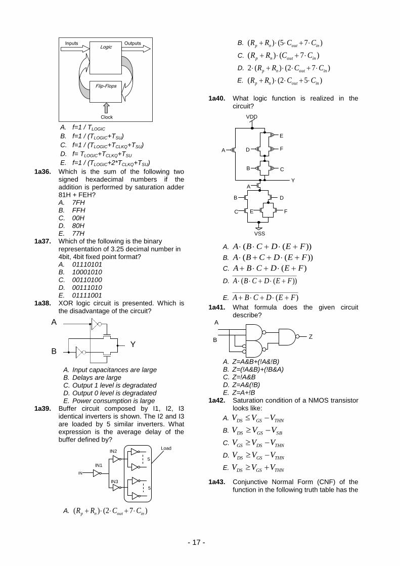
A. f=1 / TLOGIC
B. f=1 / (TLOGIC+TSU)
C. f=1 / (TLOGIC+TCLKQ+TSU)
D. f= TLOGIC+TCLKQ+TSU
E. f=1 / (TLOGIC+2*TCLKQ+TSU)
1a36. Which is the sum of the following two signed hexadecimal numbers if the addition is performed by saturation adder 81H + FEH? A. 7FH B. FFH C. 00H D. 80H E. 77H
1a37. Which of the following is the binary representation of 3.25 decimal number in 4bit, 4bit fixed point format? A. 01110101 B. 10001010 C. 00110100 D. 00111010 E. 01111001
1a38. XOR logic circuit is presented. Which is the disadvantage of the circuit?
A. Input capacitances are large B. Delays are large C. Output 1 level is degradated D. Output 0 level is degradated E. Power consumption is large
1a39. Buffer circuit composed by I1, I2, I3 identical inverters is shown. The I2 and I3 are loaded by 5 similar inverters. What expression is the average delay of the buffer defined by?
A. )72()( inoutnp CCRR
B. )75()( inoutnp CCRR
C. )7()( inoutnp CCRR
D. )72()(2 inoutnp CCRR
E. )52()( inoutnp CCRR
1a40. What logic function is realized in the circuit?
A. ))(( FEDCBA
B. ))(( FEDCBA
C. )( FEDCBA
D. ))(( FEDCBA
E. )( FEDCBA
1a41. What formula does the given circuit describe?
A. Z=A&B+(!A&!B) B. Z=(!A&B)+(!B&A) C. Z=!A&B D. Z=A&(!B) E. Z=A+!B
1a42. Saturation condition of a NMOS transistor looks like:
A. THNGSDS VVV
B. SBGSDS VVV
C. THNDSGS VVV
D. THNGSDS VVV
E. THNGSDS VVV
1a43. Conjunctive Normal Form (CNF) of the function in the following truth table has the
Clock
Inputs Outputs Logic
Flip-Flops
A
B
Z
A
B Y
A
E
C
D
B
F
A
B
E
C
D
F
VSS
VDD
Y
IN3
IN
IN1
IN2
5
5
Load
- 18 -
following view:
A. (!a+!b+!c)& (!a+b+c)& (!a+b+c)& (!a+!b+c) B. (a+!b+!c)& (!a+b+c)& (!a+b+c)& (!a+!b+!c) C. (!a+!b+c)& (!a+!b+c)& (!a+b+c)& (!a+!b+c) D. (a+b+c)& (!a+b+c)& (!a+b+!c)& (!a+!b+c) E. !a&!b&!c+ !a&b&!c+ a&!b&!c+ a&b&c
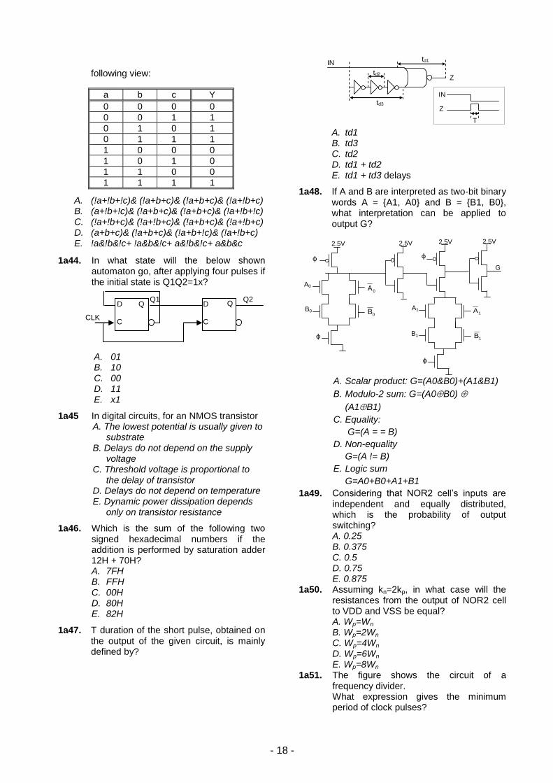
1a44. In what state will the below shown automaton go, after applying four pulses if the initial state is Q1Q2=1x?
A. 01 B. 10 C. 00 D. 11 E. x1
1a45 In digital circuits, for an NMOS transistor A. The lowest potential is usually given to
substrate B. Delays do not depend on the supply
voltage C. Threshold voltage is proportional to
the delay of transistor D. Delays do not depend on temperature E. Dynamic power dissipation depends
only on transistor resistance
1a46. Which is the sum of the following two signed hexadecimal numbers if the addition is performed by saturation adder 12H + 70H? A. 7FH B. FFH C. 00H D. 80H E. 82H
1a47. T duration of the short pulse, obtained on the output of the given circuit, is mainly defined by?
A. td1 B. td3 C. td2 D. td1 + td2 E. td1 + td3 delays
1a48. If A and B are interpreted as two-bit binary words A = {A1, A0} and B = {B1, B0}, what interpretation can be applied to output G?
A. Scalar product: G=(A0&B0)+(A1&B1)
B. Modulo-2 sum: G=(A0B0)
(A1B1)
C. Equality:
G=(A = = B)
D. Non-equality
G=(A != B)
E. Logic sum
G=A0+B0+A1+B1
1a49. Considering that NOR2 cell’s inputs are independent and equally distributed, which is the probability of output switching? A. 0.25 B. 0.375 C. 0.5 D. 0.75 E. 0.875
1a50. Assuming kn=2kp, in what case will the resistances from the output of NOR2 cell to VDD and VSS be equal? A. Wp=Wn B. Wp=2Wn C. Wp=4Wn D. Wp=6Wn E. Wp=8Wn
1a51. The figure shows the circuit of a frequency divider. What expression gives the minimum period of clock pulses?
a b c Y
0 0 0 0
0 0 1 1
0 1 0 1
0 1 1 1
1 0 0 0
1 0 1 0
1 1 0 0
1 1 1 1
td1
td2
td3
Z
IN
IN
Z
T
G
2.5V 2.5V 2.5V 2.5V
ϕ
ϕ
ϕ
ϕ
0A
1A 0B
1B
A0
B0
B1
A1
CLK C
D Q Q1 Q2
C
D Q
- 19 -
A. Tmin=tsu+tc2q+tpinv B. Tmin= tc2q+tpinv C. Tmin=tsu+thd+tc2q+tpinv D. Tmin= thd+tc2q+tpinv E. Tmin= tsu+thd+tpinv
1a52. How many digits does the thermometer code have which is obtained after modifying 4-bit binary code? A. 16 B. 4 C. 15 D. 8 E. 32
1a53. For the same size inverter what version has minimum leakage current? A. PMOS low-vt, NMOS high-vt B. PMOS standard-vt, NMOS high-vt C. PMOS high-vt, NMOS standard-vt D. PMOS high-vt, NMOS low-vt E. PMOS low-vt, NMOS standard-vt
1a54. What logic function does the circuit
implement?
A. OUT=A+B B. OUT=A&B C. OUT=!A+!B D. OUT=!A&!B
E. OUT=A!B
1a55. Which is the basic consequence of MOS transistor’s degradation due to warm carriers? A. The increase of threshold voltage B. The decrease of threshold voltage C. The increase of channel resistance D. The decrease of channel resistance E. The decrease of drain-package
disruption voltage
1a56. Assuming kn=rkp, in what case will the resistances from the output of 3NAND cell to VDD and VSS be equal? A. Wp/Wn=r B. Wp/Wn=r/9 C Wp/Wn=r/6 D. Wp/Wn=r/3 E. Wp/Wn=2r/3
1a57. Which one of the given expressions is wrong?
A. A!B = !AB
B. 1!BA = BA
C. AB =! A!B
D. A!B = !A!B
E. !AB = !(AB)
1a58. What is the minimum number of transistors in a pass gate implemented 1:4 multiplexer, assuming that normal and complemented select variables are available: A. 16 B. 12 C. 8 D. 6 E. 4
1a59. What function does the circuit implement?
A. OUT=A+B B. OUT=A&B C. OUT=!A+!B D. OUT=!A&!B
E. OUT=A!B
1a60. C capacitance is connected to the end of interconnect line with L length, line parameters are c [F/m], r [Ohm/m]. By what formula is the signal delay time in the line given? A. 0.7rc B. 0.7Lr(C+c) C. 0.7Lr(C+Lc/2) D. 0.7Lr(C+Lc) E. 0.7Lr(C/2+Lc/2)
1a61. By increasing the metal line length of interconnect in IC, the delay increases A. Linearly B. By square law C. By 3/2 law D. By 2/3 law E. By cubic law
1a62. Assuming that a p-n junction forward bias voltage is Vpn, what is the input voltage maximum safe margin?
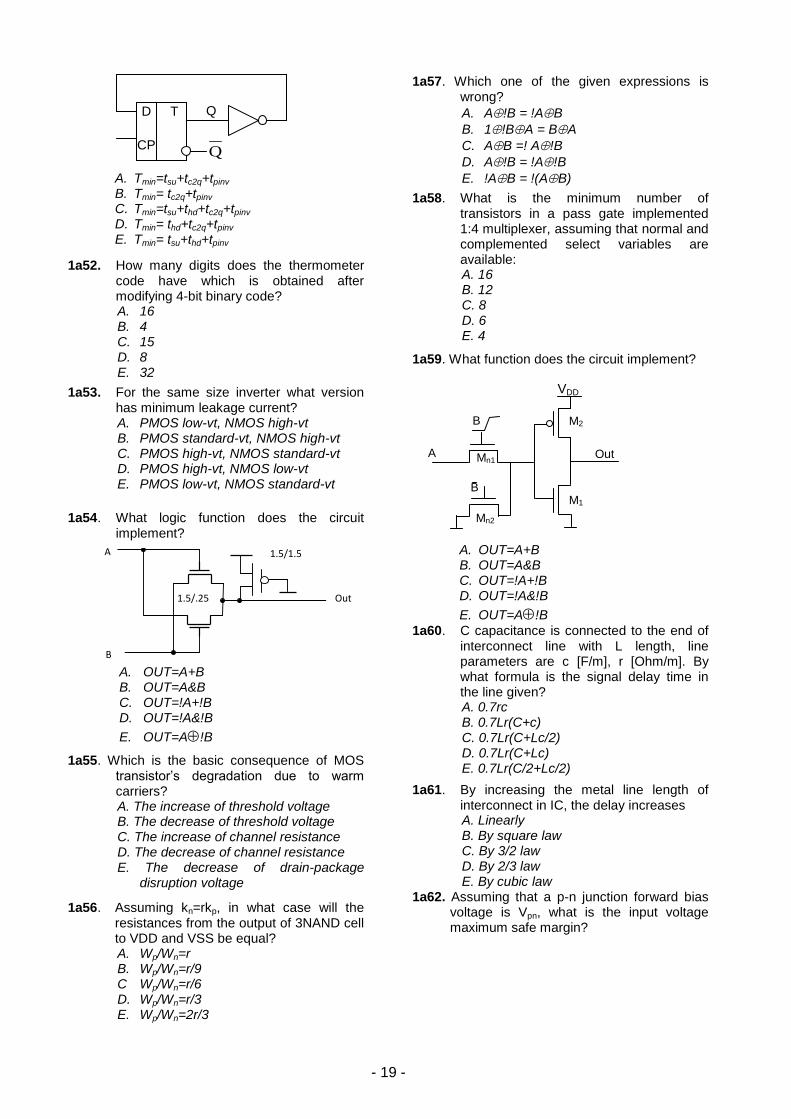
1.5/1.5
1.5/.25
A
B
Out
Out
M2
M1
Mn2
Mn1
B
A
VDD
B
Q D
CP
T
Q
- 20 -
A. VSS VinVDD
B. VSS-Vpn VinVDD-Vpn
C. VSS+Vpn VinVDD+Vpn
D. VSS-VpnVinVDD+Vpn
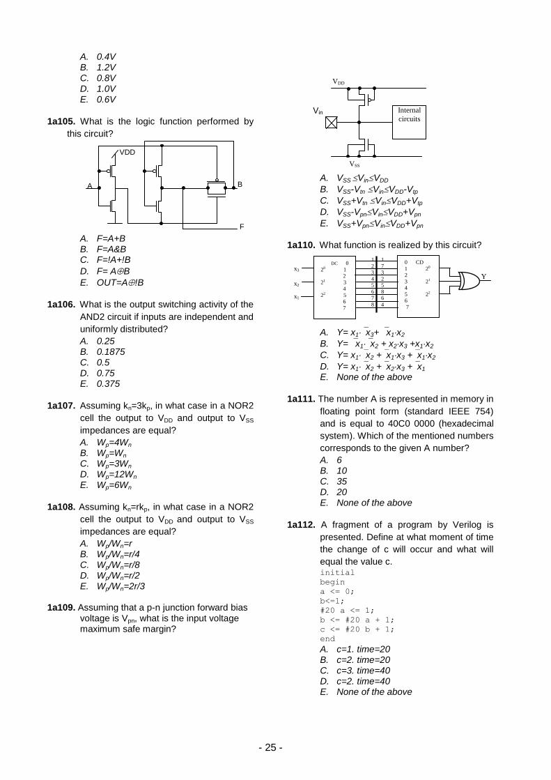
E. VSS+VpnVinVDD-Vpn 1a63. Which answer is true if VIN=VDD?
A. M1-saturated, M2-linear B. M1-linear, M2-linear C. M1- linear, M2- saturated D. M1-saturated, M2-saturated E. None
1a64. In what case is the short connection current missing in a CMOS inverter? A. Vtp=Vtn B. Vtp+Vtn=0 C. Vtp+Vtn<VDD D. |Vtp|+Vtn<VDD E. |Vtp|+Vtn<VDD/2
1a65. What equation describes JK flip-flop function? A. Q+=Q&J + !Q&K B. Q+=!Q&J + Q&K C. Q+=!Q&J + Q&!K D. Q+=Q&!J + !Q&K E. Q+=Q&J + !Q&!K
1a66. At passing from one technology to the other, transistors are scaled by S <1 coefficient due to which the gate capacitance of a transistor with minimal sizes, depending on S: A. Increases linearly B. Decreases linearly C. Increases by square law D. Decreases by square law E. Does not change
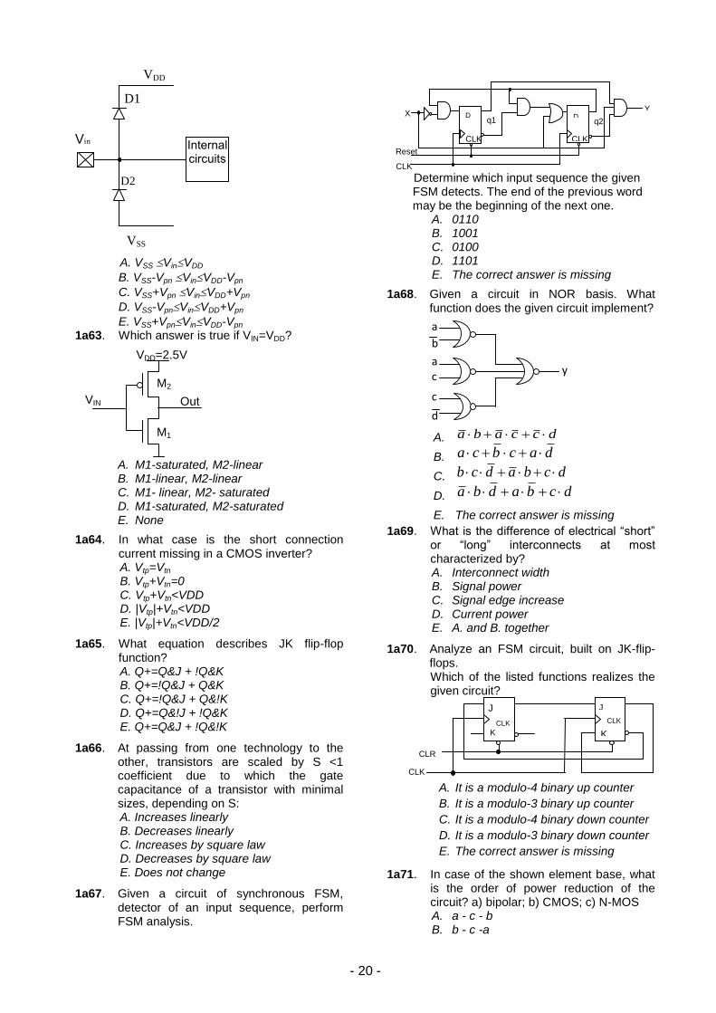
1a67. Given a circuit of synchronous FSM, detector of an input sequence, perform FSM analysis.
Determine which input sequence the given FSM detects. The end of the previous word may be the beginning of the next one.
A. 0110 B. 1001 C. 0100 D. 1101 E. The correct answer is missing
1a68. Given a circuit in NOR basis. What function does the given circuit implement?
A. dccaba
B. dacbca
C. dcbadcb
D. dcbadba
E. The correct answer is missing
1a69. What is the difference of electrical “short” or “long” interconnects at most characterized by? A. Interconnect width B. Signal power C. Signal edge increase D. Current power E. A. and B. together
1a70. Analyze an FSM circuit, built on JK-flip-flops. Which of the listed functions realizes the given circuit?
A. It is a modulo-4 binary up counter
B. It is a modulo-3 binary up counter
C. It is a modulo-4 binary down counter
D. It is a modulo-3 binary down counter
E. The correct answer is missing
1a71. In case of the shown element base, what is the order of power reduction of the circuit? a) bipolar; b) CMOS; c) N-MOS A. a - c - b B. b - c -a
a
a c
b
c
d
y
CLK CLK
D D Y
q2 q1 X
CLK
Reset
Out
M2
M1
VIN
VDD=2.5V
VDD
D1
D2
Vin
VSS
Internal circuits
CLK
CLR
J
K CLK
J
K
CLK
- 21 -
C. a - b - c D. b - a - c E. c - b - a
1a72. It is required to construct 64:1 multiplexer using 8:1 multiplexer. How many 8:1 multiplexers are needed? A. 8 MUX 8:1 B. 9 MUX 8:1 C. 10 MUX 4:1 D. 11 MUX 8:1 E. The correct answer is missing
1a73. Which of the below listed criteria of organizing interconnects more contributes to the increase of performance? A. Increase of the number of
interconnects layers B. Similarity of interconnects length C. Increase of the number of vias D. Reduction of critical path of signal
processing E. A. and B. together
1a74. The logic of which circuit presented by VHDL code is senseless or wrong? A. process (clock) begin Y <= A and B; end process; B. process (A) begin A <= A + 1; end process; C. process (A) begin Y <= A + 1; end process; D. process (A, B) begin Y <= A and B; end process; E. process (reset_n, clock) begin if (reset_n = '0') then Y <= 0; elsif (clock'EVENT and clock = '1')
then Y <= A and B; end if; end process;
1a75. Given F(x1,x2,x3) = x1 x2 x2x3 function. Which of the given expressions corresponds to the given function?
A. F = x1x2 + x1x3 + x1x2x3
B. F = x1x2 + x1x3 + x1x2x3
C. F = x1x2 + x1x2 + x2x3
D. F = x1x2 + x2x3 + x1x3 x2
E. F = x1x2 + x1x2 + x2x3
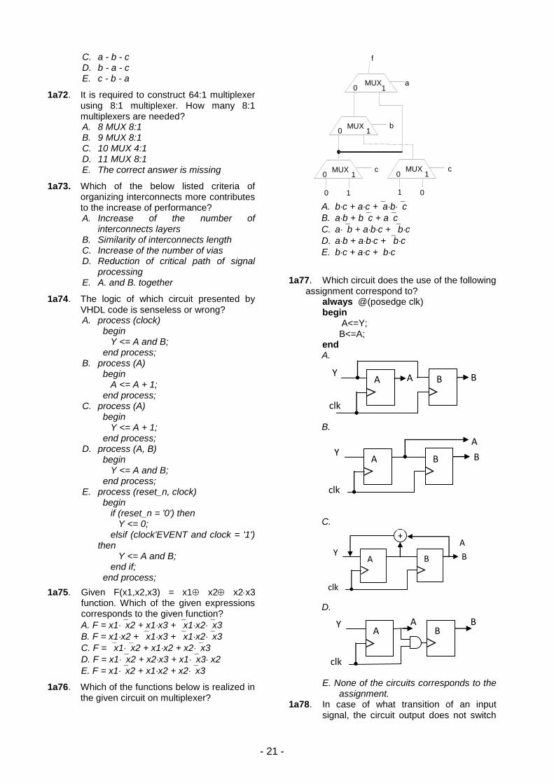
1a76. Which of the functions below is realized in the given circuit on multiplexer?
A. bc + ac +abc
B. ab + bc + ac
C. ab + abc + bc
D. ab + abc + bc
E. bc + ac + bc
1a77. Which circuit does the use of the following assignment correspond to?
always @(posedge clk) begin
A<=Y; B<=A;
end A.
B.
C.
D.
E. None of the circuits corresponds to the
assignment. 1a78. In case of what transition of an input
signal, the circuit output does not switch
MUX c
1
0 1
MUX
f
a
0 1
MUX
b
0 1
0
MUX c
0
0 1
1
A B B A Y
clk
A B B
A Y
clk
A B B
A Y
clk
+
A B
B A Y
clk
- 22 -
and X node switches?
A. AB=00->01 B. AB=00->11 C. AB=01->10 D. AB=11->00 E. AB=10->00
1a79. For what purpose is Low-Doped-Drain (LDD) region created? A. To increase threshold voltage B. To increase saturation voltage C. To increase gate-source break-down
voltage D. To reduce gate capacitance E. To increase gate’s oxide break-down
voltage
1a80. The first stage of 12-input 2-stage decoder is implemented by 3AND cells, and the second one - by 4AND cells. How many 3AND cells are there in the first stage? A. 16 B. 24 C. 32 D. 8 E. 64
1a81. Considering that memory array has equal number of 1-bit cells in lines and columns, define how many word lines 10 address bit memory has if the word length is 4 bits. A. 32 B. 64 C. 128 D. 10242 E. 256
1a82. What logic function does the circuit implement?
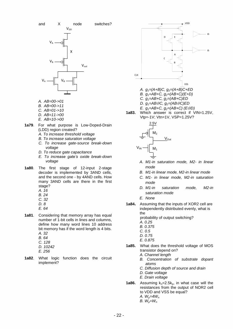
A. g1=(A+B)C, g2=(A+B)C+ED B. g1=AB+C, g2=(AB+C)(E+D) C. g1=AB+C, g2=(AB+C)ED
D. g1=ABC, g2=(ABC)ED
E. g1=AB+C, g2=(AB+C) (ED) 1a83. Which answer is correct if VIN=1.25V,
Vtp=-1V; Vtn=1V, VSP=1.25V?
A. M1-in saturation mode, M2- in linear
mode
B. M1-in linear mode, M2-in linear mode
C. M1- in linear mode, M2-in saturation
mode
D. M1-in saturation mode, M2-in
saturation mode
E. None
1a84. Assuming that the inputs of XOR2 cell are
independently distributed evenly, what is the probability of output switching? A. 0.25 B. 0.375 C. 0.5 D. 0.75 E. 0.875
1a85. What does the threshold voltage of MOS transistor depend on? A. Channel length B. Concentration of substrate dopant
atoms C. Diffusion depth of source and drain D. Gate voltage E. Drain voltage
1a86. Assuming kn=2.5kp, in what case will the resistances from the output of NOR2 cell to VDD and VSS be equal? A. Wp=4Wn B. Wp=Wn
VA
VB VA
VB
VDD
X
Vout
CLK
g 1
g 2
VDD
VSS
A
B
C
D E
M2
M1 VIN
2.5V
VOut
- 23 -
C. Wp=2Wn D. Wp=10Wn E. Wp=5Wn
1a87. Assuming kn=rkp, in what case will the resistances from the output of 4NAND cell to VDD and VSS be equal? A. Wp/Wn=r B. Wp/Wn=r/8 C. Wp/Wn=r/4 D. Wp/Wn=r/16 E. Wp/Wn=2r
1a88. The figure shows the circuit of a frequency divider.
What expression gives the minimum period of clock pulses?
A. Tmin=tsu+tc2q+2tpinv
B. Tmin= tc2q+2tpinv
C. Tmin=tsu+thd+tc2q+2tpinv
D. Tmin= thd+tc2q+2tpinv
E. Tmin= tsu+thd+2tpinv
1a89. When passing from one technology node to another, transistors are scaled by S <1 coefficient due to which the gate capacitance of a transistor with minimum sizes depends on S (assuming gate oxide thickness does not change): A. Increases by square law B. Decreases by square law C. Increases linearly D. Decreases by cubic law E. Does not change
1a90. Before reading from 1T DRAM cell, the bitline should: A. Discharge to VSS B. Discharge to Vt C. Discharge to VDD D. Charge to VDD/2 E. Charge to VDD-Vt
1a91. For the same size inverter what version has the minimum input capacitance? A. PMOS low-vt, NMOS high-vt B. PMOS standard-vt, NMOS high-vt C. PMOS high-vt, NMOS standard-vt D. PMOS high-vt, NMOS low-vt E. PMOS low-vt, NMOS standard-vt
1a92. What is the minimum number of transistors in a pass gate implemented 1:4 multiplexer, assuming that normal and complemented select variables are available? A. 16 B. 12 C. 8 D. 6 E. 4
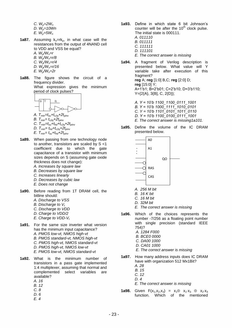
1a93. Define in which state 6 bit Johnson’s counter will be after the 10
th clock pulse.
The initial state is 000111. A. 011110 B. 011111 C. 111111 D. 111101 E. The correct answer is missing
1a94. A fragment of Verilog description is presented below. What value will Y variable take after execution of this fragment? reg A; reg [1:0] B,C; reg [2:0] D; reg [15:0] Y; A=1’b1; B=2’b01; C=2’b10; D=3’b110; Y={2{A}, 3{B], C, 2{D}};
A. Y = 10’b 1100_1100_0111_1001 B. Y = 10’b 1000_1111_1010_0101 C. Y = 10’b 1101_0101_1011_0110 D. Y = 10’b 1100_0100_0111_1001 E. The correct answer is missing1a101.
1a95. Define the volume of the IC DRAM presented below.
A. 256 M bit B. 16 K bit C. 16 M bit D. 32M bit E. The correct answer is missing
1a96. Which of the choices represents the number -7/256 as a floating point number with single precision (standard IEEE 754)? A. 1284 F000 B. BCE0 0000 C. DA00 1000 D. CA01 1000 E. The correct answer is missing
1a97. How many address inputs does IC DRAM have with organization 512 Mx1Bit? A. 28
B. 15 C. 12 D. 4 E. The correct answer is missing
1a98. Given F(x1,x2,x3) = x1 x1x3 x2x3 function. Which of the mentioned
Q D
T
A0
A1
A13
WE
RAS
CAS
QO
- 24 -
expressions corresponds to the given function?
A. F =x2x3 + x1x3
B. F = x1x2 + x1x3 +x1x2x3
C. F = x1x2 + x1x2 + x2x3
D. F = x1x2 + x1x2 + x2x3
E. The correct answer is missing
1a99. Which size does IC ROM have, implementing combinational multiplication of two 8 bit numbers?
A. 128K8
B. 25616 C. 64Kx16
D. 256K16 E. The correct answer is missing
1a100. How many ICs with 512Kx8 organization are required to implement static memory module of 8M 16 bit words size? A. 16 B. 32 C. 8 D. 24 E. The correct answer is missing
1a101. The following examples are expected to be models of logical shifter (written in Verilog HDL). Which of these examples will serve as pure combinational logic? 1) wire [7:0] my_signal; assign my_signal=my_signal<<1;
2) reg [7:0] my_signal; always @ (*) begin
my_signal = my_signal << 1;
end
3) reg [7:0] my_signal; always @ (posedge clock) begin
my_signal <= my_signal << 1;
end
Select the only correct version of these four possible answers: A. Only example 1) is the correct one B. Only example 2) is the correct one C. Only example 3) is the correct one D. Only examples 1) and 2) are the
correct ones E. All examples are correct
1a102. The following examples are expected to be models of logical "NOT" cell (written in Verilog HDL). Which of these examples will serve as correct combinational logic? 1) module not_cell (input_sig,
output_sig); input input_sig;
output output_sig;
always @ (*) begin
output_sig = 1'b1;
if (input_sig == 1'b1)
begin
output_sig = 1'b0;
end
end
endmodule
2) module not_cell (input_sig, output_sig);
input input_sig;
output output_sig;
always @ (*) begin
if (input_sig == 1'b1)
begin
output_sig = 1'b0;
end
else begin
output_sig = 1'b1;
end
end
endmodule
3) module not_cell (input_sig, output_sig);
input input_sig;
output output_sig;
always @ (input_sig) begin
if (input_sig == 1'b1)
begin
output_sig = 1'b0;
end
else begin
output_sig = 1'b1;
end
end
endmodule
Select the only correct version of these four possible answers: A. Only example 1) is the correct one B. Only example 2) is the correct one C. Only example 3) is the correct one D. All examples are incorrect E. All examples are correct.
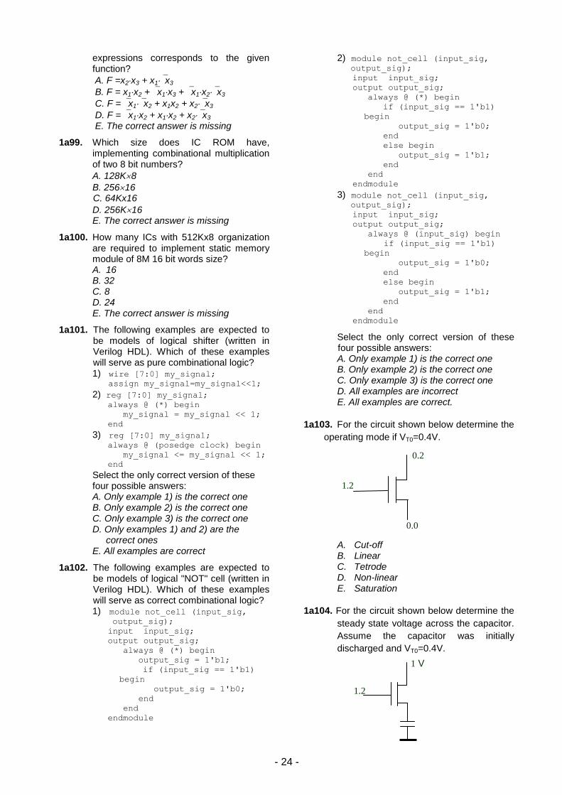
1a103. For the circuit shown below determine the
operating mode if VT0=0.4V.
A. Cut-off B. Linear C. Tetrode D. Non-linear E. Saturation
1a104. For the circuit shown below determine the
steady state voltage across the capacitor.
Assume the capacitor was initially
discharged and VT0=0.4V.
0.2
V
0.0
V
1.2
V
1 V
1.2
V
- 25 -
A. 0.4V B. 1.2V C. 0.8V D. 1.0V E. 0.6V
1a105. What is the logic function performed by
this circuit?
A. F=A+B B. F=A&B C. F=!A+!B
D. F= AB
E. OUT=A!B
1a106. What is the output switching activity of the
AND2 circuit if inputs are independent and
uniformly distributed? A. 0.25 B. 0.1875 C. 0.5 D. 0.75 E. 0.375
1a107. Assuming kn=3kp, in what case in a NOR2
cell the output to VDD and output to VSS
impedances are equal? A. Wp=4Wn B. Wp=Wn C. Wp=3Wn D. Wp=12Wn E. Wp=6Wn
1a108. Assuming kn=rkp, in what case in a NOR2
cell the output to VDD and output to VSS
impedances are equal? A. Wp/Wn=r B. Wp/Wn=r/4 C. Wp/Wn=r/8 D. Wp/Wn=r/2 E. Wp/Wn=2r/3
1a109. Assuming that a p-n junction forward bias
voltage is Vpn, what is the input voltage maximum safe margin?
A. VSS VinVDD
B. VSS-Vtn VinVDD-Vtp
C. VSS+Vtn VinVDD+Vtp
D. VSS-VpnVinVDD+Vpn
E. VSS+VpnVinVDD+Vpn
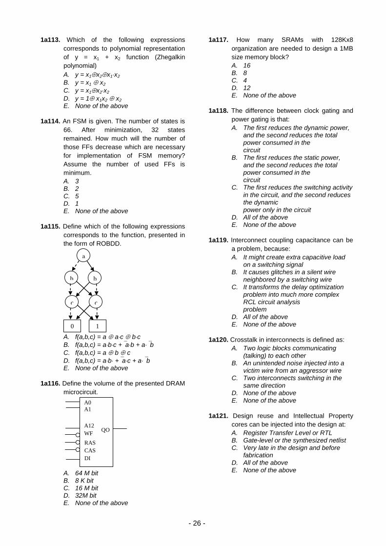
1a110. What function is realized by this circuit?
A. Y= x1x3+ x1x2
B. Y= x1x2 + x2x3 +x1x2
C. Y= x1x2 +x1x3 +x1x2
D. Y= x1x2 +x2x3 +x1 E. None of the above
1a111. The number A is represented in memory in
floating point form (standard IEEE 754)
and is equal to 40C0 0000 (hexadecimal
system). Which of the mentioned numbers
corresponds to the given A number? A. 6 B. 10 C. 35 D. 20 E. None of the above
1a112. A fragment of a program by Verilog is
presented. Define at what moment of time
the change of c will occur and what will
equal the value c. initial
begin
a <= 0;
b<=1;
#20 a <= 1;
b <= #20 a + 1;
c <= #20 b + 1;
end
A. c=1. time=20 B. c=2. time=20 C. c=3. time=40 D. c=2. time=40 E. None of the above
x3
x2
x1
DC 0
20 1
2
21 3
4
22 5
6
7
0 CD
1 20
2
3 21
4
5 22
6
7
1 1
2 7
3 3
4 2
5 5
6 8
7 6
8 4
Y
VSS
VDD
Internal
circuits Vin
A
VDD
B
F
- 26 -
1a113. Which of the following expressions
corresponds to polynomial representation
of y = x1 + x2 function (Zhegalkin
polynomial) A. y = x1x2x1x2
B. y = x1 x2
C. y = x1x2x2
D. y = 1 x1x2 x2 E. None of the above
1a114. An FSM is given. The number of states is
66. After minimization, 32 states
remained. How much will the number of
those FFs decrease which are necessary
for implementation of FSM memory?
Assume the number of used FFs is
minimum. A. 3 B. 2 C. 5 D. 1 E. None of the above
1a115. Define which of the following expressions
corresponds to the function, presented in
the form of ROBDD.
A. f(a,b,c) = a ac bc
B. f(a,b,c) = abc +ab + ab
C. f(a,b,c) = a b c
D. f(a,b,c) = ab +ac + ab E. None of the above
1a116. Define the volume of the presented DRAM
microcircuit.
A. 64 M bit B. 8 K bit C. 16 M bit D. 32M bit E. None of the above
1a117. How many SRAMs with 128Kx8
organization are needed to design a 1MB
size memory block? A. 16 B. 8 C. 4 D. 12 E. None of the above
1a118. The difference between clock gating and
power gating is that: A. The first reduces the dynamic power,
and the second reduces the total power consumed in the circuit
B. The first reduces the static power, and the second reduces the total power consumed in the circuit
C. The first reduces the switching activity in the circuit, and the second reduces the dynamic power only in the circuit
D. All of the above E. None of the above
1a119. Interconnect coupling capacitance can be
a problem, because: A. It might create extra capacitive load
on a switching signal B. It causes glitches in a silent wire
neighbored by a switching wire C. It transforms the delay optimization
problem into much more complex RCL circuit analysis problem
D. All of the above E. None of the above
1a120. Crosstalk in interconnects is defined as: A. Two logic blocks communicating
(talking) to each other B. An unintended noise injected into a
victim wire from an aggressor wire C. Two interconnects switching in the
same direction D. None of the above E. None of the above
1a121. Design reuse and Intellectual Property
cores can be injected into the design at: A. Register Transfer Level or RTL B. Gate-level or the synthesized netlist C. Very late in the design and before
fabrication D. All of the above E. None of the above
W
E
A0
A1
A12
WF
RAS
CAS
DI
QO
а
b
c
b
c
0 1
- 27 -
1a122. One of the main problems in RISC
processors that is addressed by ARM
processor is: A. 64 general purpose registers that can
be used by the user in any operational mode
B. ARM has a compressed THUMB mode that reduce the code density by 30 to 40%
C. Complex instruction set in ARM that allows variable instruction length
D. All of the above E. None of the above
1a123. CUDA language is used to program
GPUs, one of the main reasons to use
such language instead of any other
programming language because: A. Most other languages such as C,
Java, and Fortran run serially B. It is based on a parallel programming
model C. The need of a new language to adapt
to the new processor shift from a single core to many-core
D. All of the above E. None of the above
1a124. CUDA architecture model uses a host and
a device: A. The host is a GPP that runs the serial
part of a program and the device is a GPU that runs the parallel part of the program
B. The host is a GPU that runs the serial part of a program and the device is a GPP that runs the parallel part of the program
C. Host and device can be used independently from the nature of the code (whether serial or parallel) without any implications on the overall performance
D. All of the above E. None of the above
1a125. In which region of operation a MOSFET is
usually used in digital circuits? A. Cut-off and Saturation regions B. Saturation and triode regions C. Cut-off and triode regions D. Saturation region only E. None of the above
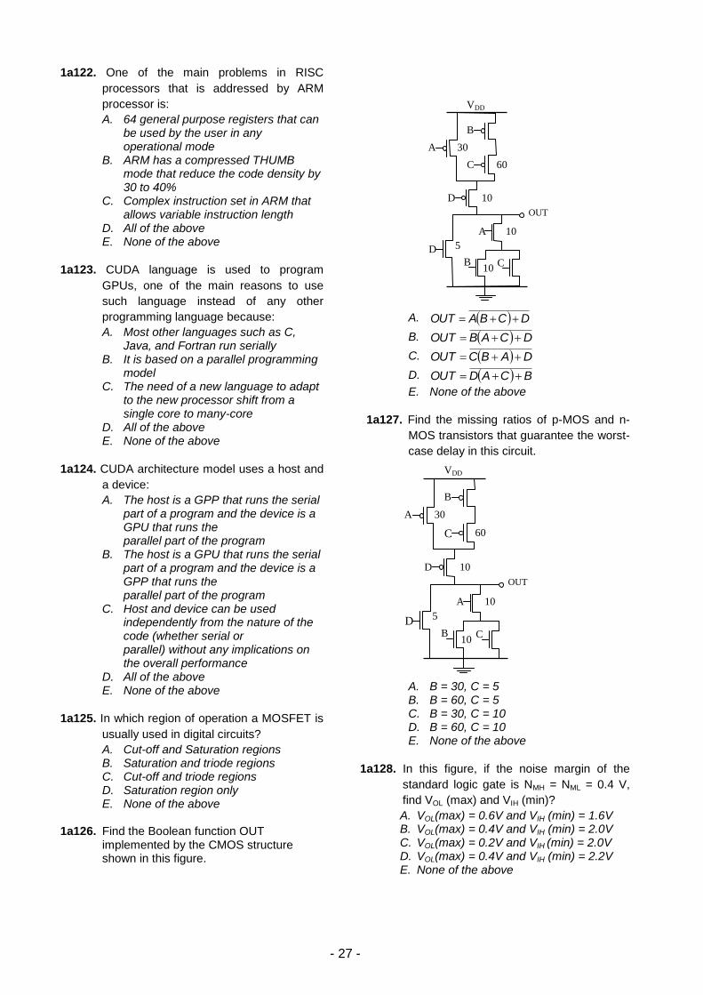
1a126. Find the Boolean function OUT
implemented by the CMOS structure shown in this figure.
A. DCBAOUT
B. DCABOUT
C. DABCOUT
D. BCADOUT
E. None of the above
1a127. Find the missing ratios of p-MOS and n-
MOS transistors that guarantee the worst-
case delay in this circuit.
A. B = 30, C = 5 B. B = 60, C = 5 C. B = 30, C = 10 D. B = 60, C = 10 E. None of the above
1a128. In this figure, if the noise margin of the
standard logic gate is NMH = NML = 0.4 V,
find VOL (max) and VIH (min)? A. VOL(max) = 0.6V and VIH (min) = 1.6V B. VOL(max) = 0.4V and VIH (min) = 2.0V C. VOL(max) = 0.2V and VIH (min) = 2.0V D. VOL(max) = 0.4V and VIH (min) = 2.2V E. None of the above
A
B
C
C B
A
D
D
VDD
30
60
10
10
5
10
OUT
A
B
C
C B
A
D
D
VDD
30
60
10
10
5
10
OUT
- 28 -
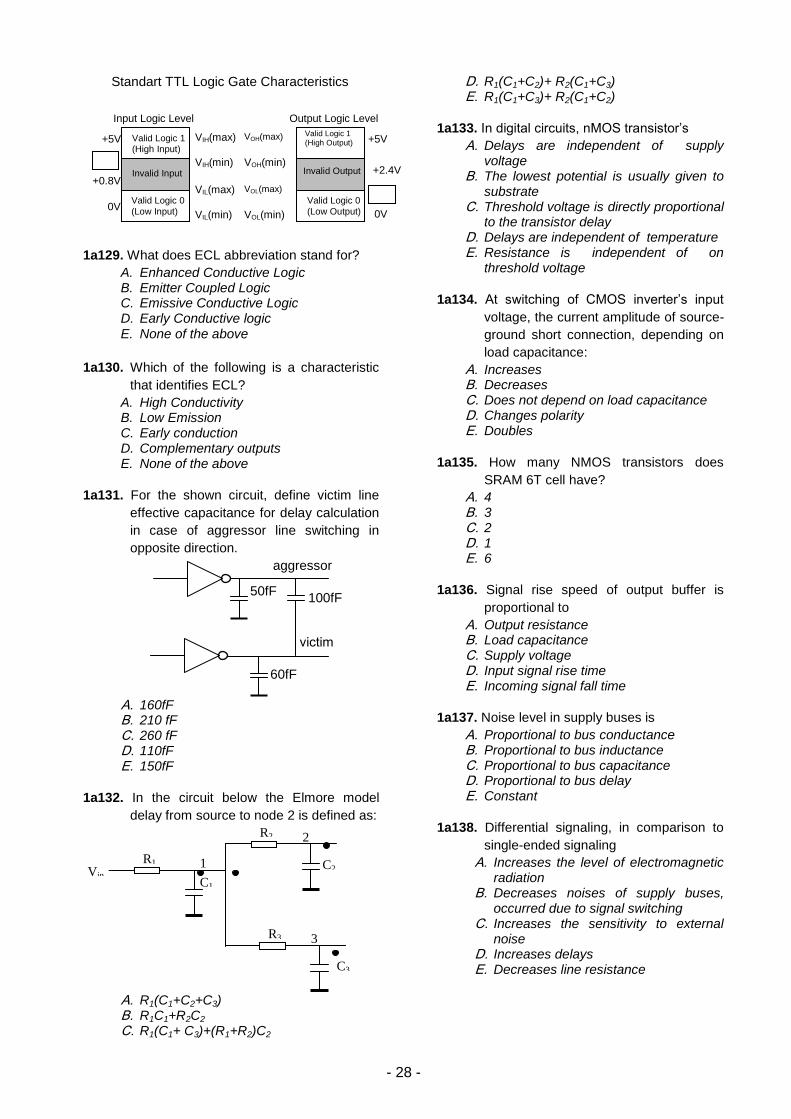
Standart TTL Logic Gate Characteristics
1a129. What does ECL abbreviation stand for? A. Enhanced Conductive Logic B. Emitter Coupled Logic C. Emissive Conductive Logic D. Early Conductive logic
E. None of the above
1a130. Which of the following is a characteristic
that identifies ECL? A. High Conductivity B. Low Emission C. Early conduction D. Complementary outputs E. None of the above
1a131. For the shown circuit, define victim line
effective capacitance for delay calculation
in case of aggressor line switching in
opposite direction.
A. 160fF B. 210 fF C. 260 fF D. 110fF E. 150fF
1a132. In the circuit below the Elmore model
delay from source to node 2 is defined as:
A. R1(C1+C2+C3) B. R1C1+R2C2 C. R1(C1+ C3)+(R1+R2)C2
D. R1(C1+C2)+ R2(C1+C3) E. R1(C1+C3)+ R2(C1+C2)
1a133. In digital circuits, nMOS transistor’s
A. Delays are independent of supply voltage
B. The lowest potential is usually given to substrate
C. Threshold voltage is directly proportional to the transistor delay
D. Delays are independent of temperature E. Resistance is independent of on
threshold voltage
1a134. At switching of CMOS inverter’s input
voltage, the current amplitude of source-
ground short connection, depending on
load capacitance:
A. Increases B. Decreases C. Does not depend on load capacitance D. Changes polarity E. Doubles
1a135. How many NMOS transistors does
SRAM 6T cell have?
A. 4 B. 3 C. 2 D. 1 E. 6
1a136. Signal rise speed of output buffer is
proportional to
A. Output resistance B. Load capacitance C. Supply voltage D. Input signal rise time E. Incoming signal fall time
1a137. Noise level in supply buses is
A. Proportional to bus conductance B. Proportional to bus inductance C. Proportional to bus capacitance D. Proportional to bus delay E. Constant
1a138. Differential signaling, in comparison to
single-ended signaling
A. Increases the level of electromagnetic radiation
B. Decreases noises of supply buses, occurred due to signal switching
C. Increases the sensitivity to external noise
D. Increases delays E. Decreases line resistance
R1
C1 Vin
R3
C3
R2
C2 1
2
3
60fF
100fF 50fF
aggressor
victim
Valid Logic 1 (High Input)
Invalid Input
Valid Logic 0
(Low Input)
Valid Logic 1 (High Output)
Invalid Output
Valid Logic 0
(Low Output)
VIH(max)
VIH(min)
VIL(max)
VIL(min)
VOH(max)
VOH(min)
VOL(max)
VOL(min)
Input Logic Level Output Logic Level
+5V
+0.8V
0V
+5V
+2.4V
0V
- 29 -
1a139. For efficient IC protection, the protective
circuits towards ESD current should
have:
A. Small resistance B. Large resistance C. Small capacitance D. Large inductance E. Little losses
1a140. What logic function is implemented?
A. !(x(y+z)) B. x(y+z) C. x+yz D. !x+yz E. !xy+z
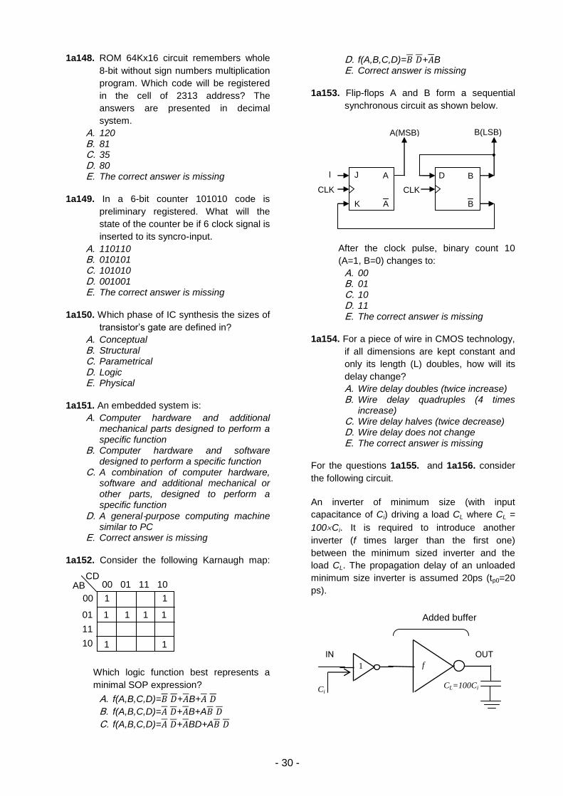
1a141. What logic function is implemented?
A. pn=anbn
B. pn=!(anbn)
C. pn=!anbn
D. pn=!anbn E. pn=!an+bn
1a142. Define the maximum permissible
absolute value of noise, imposed on
logic 1 in inputs of a CMOS inverter if
the supply voltage is 1 V, inverter’s VTC
transient domain is within [0.3V-0.6V]
range of input voltage.
A. 0.3 V B. 0.6 V C. 0.4 V D. 0.7 V E. 0.5 V
1a143. Considering that the inputs of NOR3 cell
are independent and equally distributed,
which is the probability of output
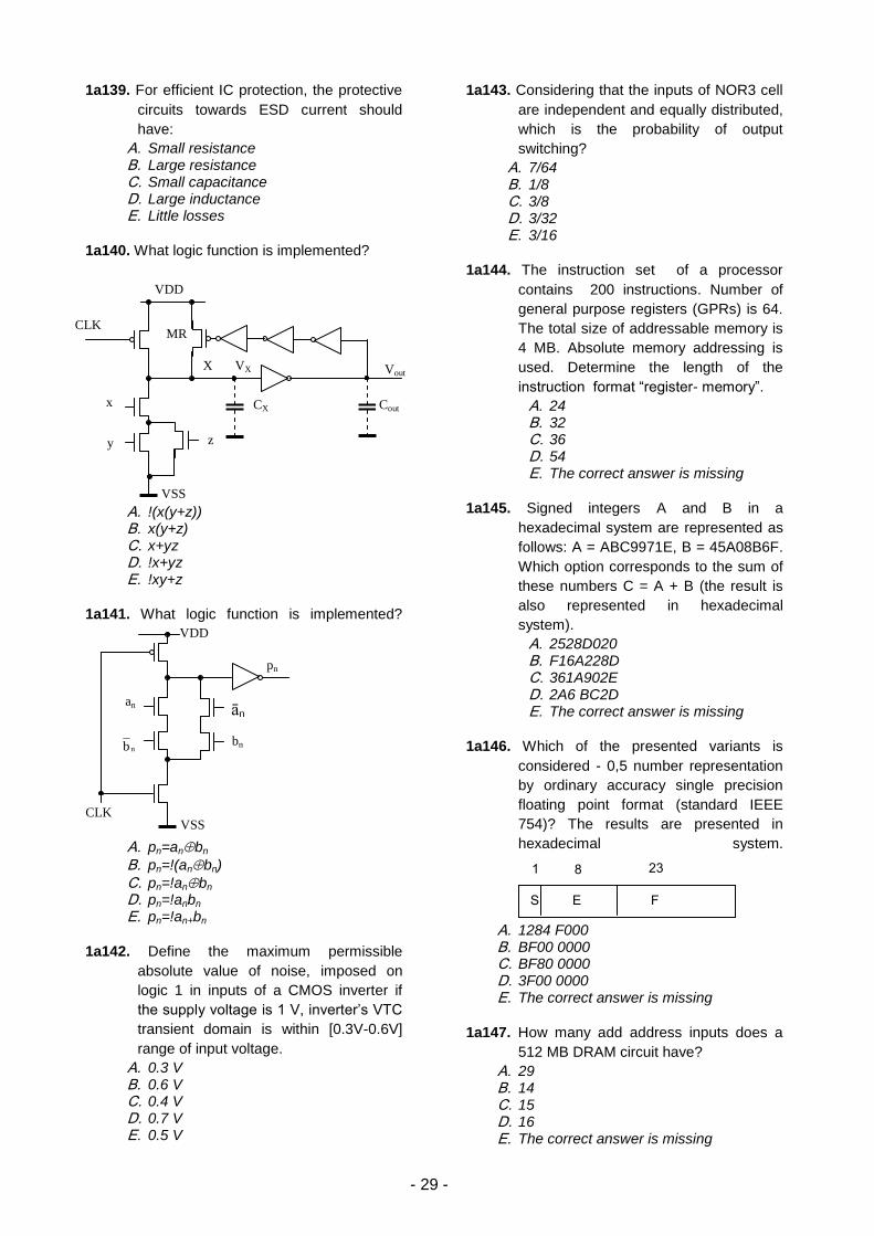
switching?
A. 7/64 B. 1/8 C. 3/8 D. 3/32 E. 3/16
1a144. The instruction set of a processor
contains 200 instructions. Number of
general purpose registers (GPRs) is 64.
The total size of addressable memory is
4 MB. Absolute memory addressing is
used. Determine the length of the
instruction format “register- memory”.
A. 24 B. 32 C. 36 D. 54 E. The correct answer is missing
1a145. Signed integers A and B in a
hexadecimal system are represented as
follows: A = ABC9971E, B = 45A08B6F.
Which option corresponds to the sum of
these numbers C = A + B (the result is
also represented in hexadecimal
system).
A. 2528D020 B. F16A228D C. 361A902E D. 2A6 BC2D E. The correct answer is missing
1a146. Which of the presented variants is
considered - 0,5 number representation
by ordinary accuracy single precision
floating point format (standard IEEE
754)? The results are presented in
hexadecimal system.
A. 1284 F000 B. BF00 0000 C. BF80 0000 D. 3F00 0000 E. The correct answer is missing
1a147. How many add address inputs does a
512 MB DRAM circuit have?
A. 29 B. 14 C. 15 D. 16 E. The correct answer is missing
S E F
8 23 1
CLK
pn
VDD
VSS
nb
an ān
bn
CLK
Vout
VDD
VSS
y
x
X
MR
z
CX Cout
VX
- 30 -
1a148. ROM 64Kx16 circuit remembers whole
8-bit without sign numbers multiplication
program. Which code will be registered
in the cell of 2313 address? The
answers are presented in decimal
system.
A. 120 B. 81 C. 35 D. 80 E. The correct answer is missing
1a149. In a 6-bit counter 101010 code is
preliminary registered. What will the
state of the counter be if 6 clock signal is
inserted to its syncro-input.
A. 110110 B. 010101 C. 101010 D. 001001 E. The correct answer is missing
1a150. Which phase of IC synthesis the sizes of
transistor’s gate are defined in?
A. Conceptual B. Structural C. Parametrical D. Logic E. Physical
1a151. An embedded system is:
A. Computer hardware and additional mechanical parts designed to perform a specific function
B. Computer hardware and software designed to perform a specific function
C. A combination of computer hardware, software and additional mechanical or other parts, designed to perform a specific function
D. A general‐purpose computing machine similar to PC
E. Correct answer is missing
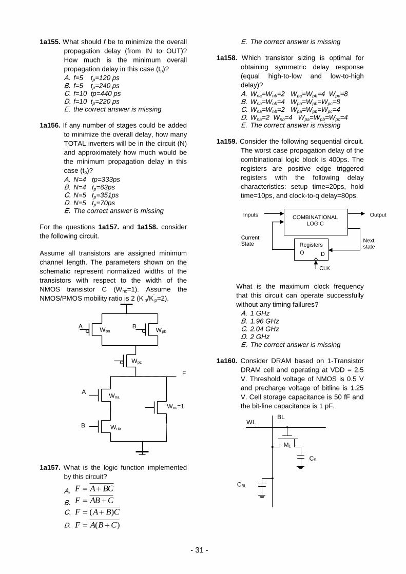
1a152. Consider the following Karnaugh map:
Which logic function best represents a
minimal SOP expression?
A. f(A,B,C,D)= + B+
B. f(A,B,C,D)= + B+A
C. f(A,B,C,D)= + BD+A
D. f(A,B,C,D)= + B E. Correct answer is missing
1a153. Flip-flops A and B form a sequential
synchronous circuit as shown below.
After the clock pulse, binary count 10
(A=1, B=0) changes to:
A. 00 B. 01 C. 10 D. 11 E. The correct answer is missing
1a154. For a piece of wire in CMOS technology,
if all dimensions are kept constant and
only its length (L) doubles, how will its
delay change?
A. Wire delay doubles (twice increase) B. Wire delay quadruples (4 times
increase) C. Wire delay halves (twice decrease) D. Wire delay does not change E. The correct answer is missing
For the questions 1a155. and 1a156. consider
the following circuit.
An inverter of minimum size (with input
capacitance of Ci) driving a load CL where CL =
100Ci. It is required to introduce another
inverter (f times larger than the first one)
between the minimum sized inverter and the
load CL. The propagation delay of an unloaded
minimum size inverter is assumed 20ps (tp0=20
ps).
1 f
CL=100Ci Ci
Added buffer
OUT IN
l
CLK
J
K
A
A
D
CLK
B
B
A(MSB) B(LSB)
AB CD
00 01 11 10
00
01
11
10
1 1
1 1 1 1
1 1
- 31 -
1a155. What should f be to minimize the overall
propagation delay (from IN to OUT)?
How much is the minimum overall
propagation delay in this case (tp)?
A. f=5 tp=120 ps B. f=5 tp=240 ps C. f=10 tp=440 ps D. f=10 tp=220 ps E. the correct answer is missing
1a156. If any number of stages could be added
to minimize the overall delay, how many
TOTAL inverters will be in the circuit (N)
and approximately how much would be
the minimum propagation delay in this
case (tp)?
A. N=4 tp=333ps B. N=4 tp=63ps C. N=5 tp=351ps D. N=5 tp=70ps E. The correct answer is missing
For the questions 1a157. and 1a158. consider
the following circuit.
Assume all transistors are assigned minimum
channel length. The parameters shown on the
schematic represent normalized widths of the
transistors with respect to the width of the
NMOS transistor C (Wnc=1). Assume the
NMOS/PMOS mobility ratio is 2 (K’n/K
’p=2).
1a157. What is the logic function implemented
by this circuit?
A. BCAF
B. CABF
C. CBAF )(
D. )( CBAF
E. The correct answer is missing
1a158. Which transistor sizing is optimal for
obtaining symmetric delay response
(equal high-to-low and low-to-high
delay)?
A. Wna=Wnb=2 Wpa=Wpb=4 Wpc=8 B. Wna=Wnb=4 Wpa=Wpb=Wpc=8 C. Wna=Wnb=2 Wpa=Wpb=Wpc=4 D. Wna=2 Wnb=4 Wpa=Wpb=Wpc=4 E. The correct answer is missing
1a159. Consider the following sequential circuit.
The worst case propagation delay of the
combinational logic block is 400ps. The
registers are positive edge triggered
registers with the following delay
characteristics: setup time=20ps, hold
time=10ps, and clock-to-q delay=80ps.
What is the maximum clock frequency
that this circuit can operate successfully
without any timing failures?
A. 1 GHz B. 1.96 GHz C. 2.04 GHz D. 2 GHz E. The correct answer is missing
1a160. Consider DRAM based on 1-Transistor
DRAM cell and operating at VDD = 2.5
V. Threshold voltage of NMOS is 0.5 V
and precharge voltage of bitline is 1.25
V. Cell storage capacitance is 50 fF and
the bit-line capacitance is 1 pF.
CBL
WL BL
CS
M1
Inputs
Current State
COMBINATIONAL LOGIC
Outputs
Next state
Registers
D Q
CLK
B
A B
Wnb
Wnc=1
Wpc
Wpa Wpb
A Wna
F
- 32 -
How much voltage swing is created on
the bitline when a cell storing ‘1’ is
accessed for the read operation?
A. 47.6 mV B. 35.7 mV C. 59.5 mV D. 119 mV E. The correct answer is missing
1a161. Consider the following transistor which is
in the off condition (Vgs=0<Vt=0.2 and
Vdd=1V). Assume subthreshold and
junction leakage components are both
considerable.
by applying negative VBB:
A. Both subthreshold and junction leakage decrease
B. Subthresold leakage decreases and junction leakage increases
C. Subthreshold leakage increases and junction leakage decreases
D. Both subthrehsold and junction leakage increase
E. The correct answer is missing
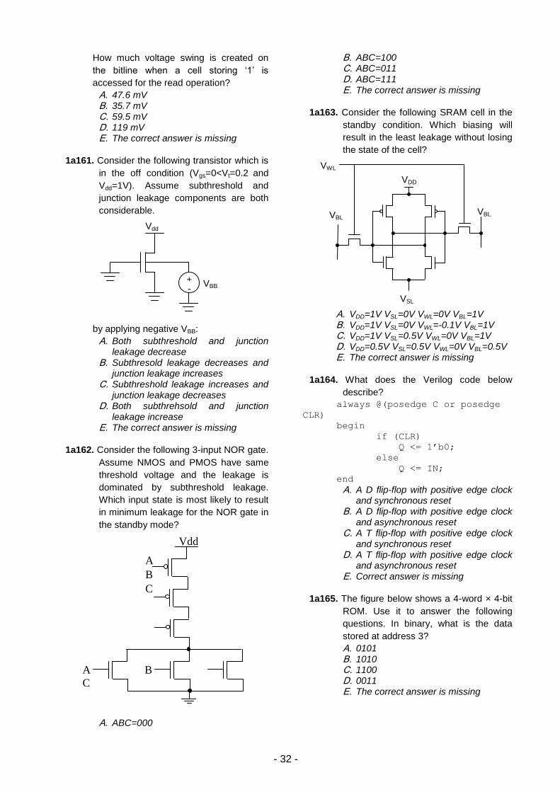
1a162. Consider the following 3-input NOR gate.
Assume NMOS and PMOS have same
threshold voltage and the leakage is
dominated by subthreshold leakage.
Which input state is most likely to result
in minimum leakage for the NOR gate in
the standby mode?
A. ABC=000
B. ABC=100 C. ABC=011 D. ABC=111 E. The correct answer is missing
1a163. Consider the following SRAM cell in the
standby condition. Which biasing will
result in the least leakage without losing
the state of the cell?
A. VDD=1V VSL=0V VWL=0V VBL=1V B. VDD=1V VSL=0V VWL=-0.1V VBL=1V C. VDD=1V VSL=0.5V VWL=0V VBL=1V D. VDD=0.5V VSL=0.5V VWL=0V VBL=0.5V E. The correct answer is missing
1a164. What does the Verilog code below
describe?
always @(posedge C or posedge
CLR)
begin
if (CLR)
Q <= 1’b0;
else
Q <= IN;
end
A. A D flip-flop with positive edge clock and synchronous reset
B. A D flip-flop with positive edge clock and asynchronous reset
C. A T flip-flop with positive edge clock and synchronous reset
D. A T flip-flop with positive edge clock and asynchronous reset
E. Correct answer is missing
1a165. The figure below shows a 4-word × 4-bit
ROM. Use it to answer the following
questions. In binary, what is the data
stored at address 3?
A. 0101 B. 1010 C. 1100 D. 0011 E. The correct answer is missing
VWL
VDD
VBL VBL
VSL
A B
C
A
B
C
Vdd
Vdd
VBB + -
- 33 -
1a166. If the inverter delay is 100 ps, what is the
frequency of a 25-stage ring oscillator?
A. 10 GHz B. 100 MHz C. 200 MHz D. 400 MHz E. The correct answer is missing
1a167. What devices do EEPROM cells use
internally (inside the chip) to make them
programmable?
A. Fuses B. SRAM cells C. Floating gate transistors D. DRAM cells E. The correct answer is missing
1a168. Which type of memory is used in on-chip
high-speed microprocessor caches?
A. SRAM B. DRAM C. FRAM D. SDRAM E. The correct answer is missing
1a169. Consider a 16x1 unfooted non-inverting
domino multiplexer implemented using
four 4-input dynamic multiplexers and a
single static CMOS logic gate. The static
CMOS logic gate that should be used is:
A. NOR B. OR C. NAND D. AND E. The correct answer is missing
1a170. What is the eight-bit code Х (х7 ... х0) that
must be submitted to the inputs of the
multiplexer to implement the logical
function BCACBACABF ?
A. 01101000 B. 00010110 C. 10010111 D. 11101001 E. The correct answer is missing
1a171. Specify the ROM capacity in bits.
A. 128 B. 256 C. 512 D. 1024 E. 2048
1a172. Which of these Verilog implementations
are synthesized into RTL description
without errors or mismatches?
A.
always @ (posedge SCLK or posedge
RESET or posedge SS) begin
if (~RESET) begin
shift_register[7:0] <=
8'b0;
end else if (~SS) begin
shift_register[7:0] <=
8'b0;
end else begin
shift_register <=
shift_register << 1;
shift_register[0] <=
MOSI;
RAM A
CS
WE
OE
CE
I
O
7
8
8
4 2 1
A B C
MS
0 . . 7
8 X
F
A1 A0
0
1
2
3
Y3 Y2 Y1 Y0

- 34 -
end
end
B.
always @ (posedge SCLK or negedge
RESET ) begin
if (~RESET) begin
shift_register[7:0] =
8'b0;
end else if (SS) begin
shift_register[7:0] =
8'b0;
end else begin
shift_register =
shift_register << 1;
shift_register[0]= MOSI;
end
end
C.
always @ (posedge SCLK or negedge
RESET or posedge SS) begin
if (~RESET) begin
shift_register[7:0]<=
8'b0;
end else if (SS) begin
shift_register[7:0] <= 8'b0;
end else begin
shift_register <=
shift_register << 1;
shift_register[0] <=
MOSI;
end
end
D.
always @ (posedge SCLK or negedge
RESET or posedge SS) begin
if (~RESET) begin
shift_register[7:0]=
8'b0;
end else if (SS) begin
shift_register[7:0]=
8'b0;
end else begin
shift_register <=
shift_register << 1;
shift_register[0] = MOSI;
end
end
E. Correct answer is missing
1a173. What is the aspect ratio of channel width
to length of n-MOS transistor for the
following parameters: gm=1.2 mA/V,
Vth=0.5V, Vgs=2V, Vds=1V, kn=120µA/V2.
A. 5 B. 10 C. 15 D. 20 E. The correct answer is missing
1a174. What statement describes properties of
equipments made using standard
integrated circuits?
A. Easy to copy, slow prototyping, small number of soldering pins, require larger PCB than ASIC, cost effective for large volume production
B. Easy to copy, fast prototyping, large number of soldering pins, require larger PCB than ASIC, cost effective for small volume production
C. Easy to copy, fast prototyping, small number of soldering pins, require smaller PCB than ASIC, cost effective for large volume production
D. Difficult to copy, slow prototyping, large number of soldering pins, require larger PCB than ASIC, cost effective for large volume production
E. Difficult to copy, fast prototyping, large number of soldering pins, require smaller PCB than ASIC, appropriate for small volume production
1a175. To obtain minimum delay CMOS
inverter, the ratio between pMOS and
nMOS width (Wp/Wn) should be:
A. n/p
B. p/n
C. pn /
- 35 -
D. np /
E. 1
1a176. The final result of AC analysis for a linear
circuit depends on:
A. Time step B. Initial condition C. Criteria for iterative loop termination D. Correct answers are A. and B. E. None of the above
1a177. If one input of an OR2 cell is at logic 1
and another transits from 1 to 0, then:
A. There is a bus conflict B. There is an illegal input C. an event occurs D. A neutral event occurs E. The correct answer is missing
1a178. The logic function implemented by the
circuit below is (VDD implies a logic “1”):
A. Y=NAND(A,B) B. Y=NOR(A,B)
C. Y=XNOR(A,B) D. Y=XOR(A,B) E. The correct answer is missing
1a179. The minimum number of 2-input NOR
gates required to implement the Boolean
function , assuming that A, B
and C are available is:
A. Three B. Four C. Five D. Six E. Seven
1a180. Assuming that all the flip-flops are in the
reset condition initially, the sequence
observed at the output pin in the circuit
shown below is:
A. 011100…. B. 001110…. C. 000111…. D. 010101…. E. The correct answer is missing
b) Problems
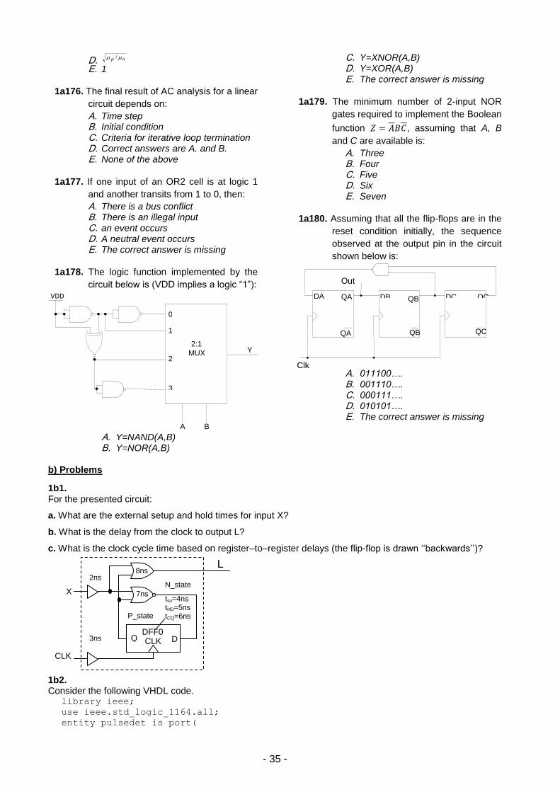
1b1. For the presented circuit:
a. What are the external setup and hold times for input X?
b. What is the delay from the clock to output L?
c. What is the clock cycle time based on register–to–register delays (the flip-flop is drawn ‘‘backwards’’)?
1b2. Consider the following VHDL code.
library ieee;
use ieee.std_logic_1164.all;
entity pulsedet is port(
L 8ns
7ns
N_state 2ns
3ns
P_state
Q CLK
tsu=4ns tHD=5ns tCQ=6ns
DFF0 D
X
CLK
Clk
DA QA DB QB DC QC
Out
QA QB QC
VDD
2:1 MUX
0
1
2
3
Y
A B
- 36 -
signal clk,reset,pulse_in: in std_logic;
signal pulse_out: out std_logic
);
end pulsedet;
architecture behavior of pulsedet is
signal dffout : std_logic_vector(2 downto 0);
begin
dffs: process(clk,reset)
begin
if (reset = ’1’) then
dffout <= “000”;
elsif (clk’event and clk=’1’) then
dffout(2) <= dffout(1);
dffout(1) <= dffout(0);
dffout(0) <= pulse_in;
end if;
end process;
pulse_out <= dffout(2) and not dffout(1);
end behavior;
Draw a diagram of logic that implements the VHDL code. (Show logic gates and D flip-flops.) 1b3. On the waveforms below, complete the waveforms for state, ld, en, and Q. The FSM is controlling the UP counter. Assume the initial state is S0.
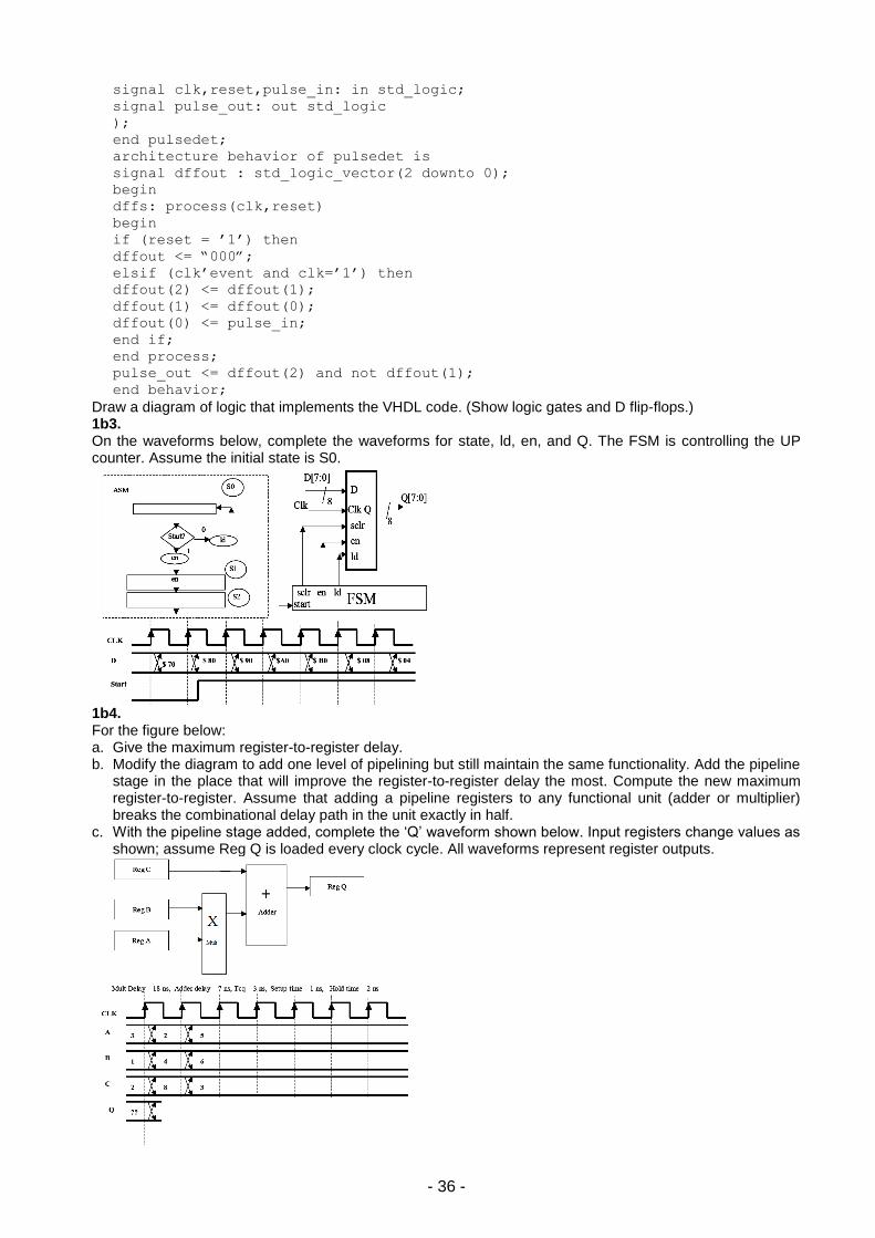
1b4. For the figure below: a. Give the maximum register-to-register delay. b. Modify the diagram to add one level of pipelining but still maintain the same functionality. Add the pipeline
stage in the place that will improve the register-to-register delay the most. Compute the new maximum register-to-register. Assume that adding a pipeline registers to any functional unit (adder or multiplier) breaks the combinational delay path in the unit exactly in half.
c. With the pipeline stage added, complete the ‘Q’ waveform shown below. Input registers change values as shown; assume Reg Q is loaded every clock cycle. All waveforms represent register outputs.
- 37 -
1b5. Design a circuit for a CMOS cell which is realized by Z=!(A(B+C)+BD) logic function.
1b6. Design a MS D-FF based on transmission gates (TG) with SET input.
1b7. Design a MS D-FF based on switching keys with SET and RESET inputs.
1b8.
Design a CMOS cell circuit which is described by Y=(1,2,6,7) function.
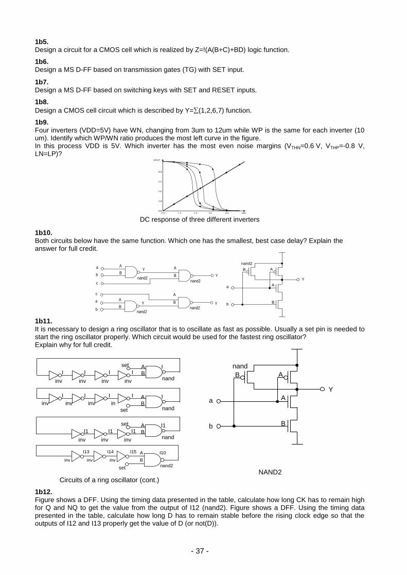
1b9. Four inverters (VDD=5V) have WN, changing from 3um to 12um while WP is the same for each inverter (10 um). Identify which WP/WN ratio produces the most left curve in the figure. In this process VDD is 5V. Which inverter has the most even noise margins (VTHN=0.6 V, VTHP=-0.8 V, LN=LP)?
DC response of three different inverters
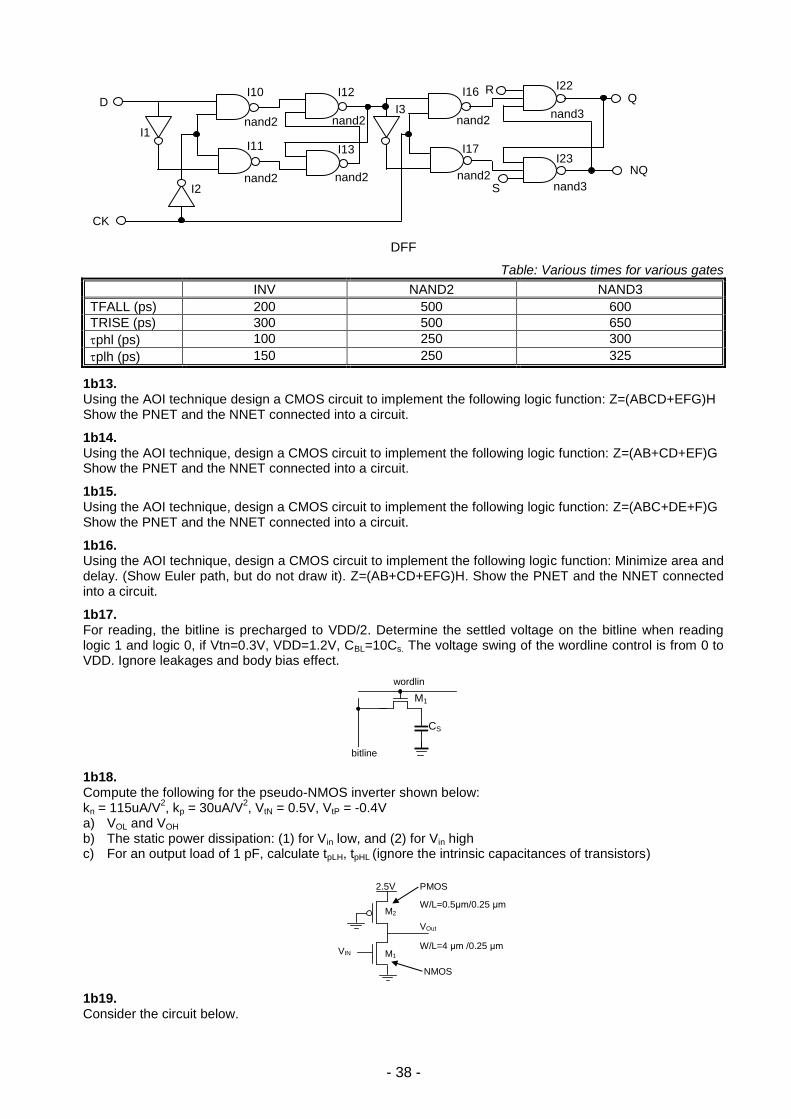
1b10. Both circuits below have the same function. Which one has the smallest, best case delay? Explain the answer for full credit.
1b11. It is necessary to design a ring oscillator that is to oscillate as fast as possible. Usually a set pin is needed to start the ring oscillator properly. Which circuit would be used for the fastest ring oscillator? Explain why for full credit.
NAND2 Circuits of a ring oscillator (cont.)
1b12. Figure shows a DFF. Using the timing data presented in the table, calculate how long CK has to remain high for Q and NQ to get the value from the output of I12 (nand2). Figure shows a DFF. Using the timing data presented in the table, calculate how long D has to remain stable before the rising clock edge so that the outputs of I12 and I13 properly get the value of D (or not(D)).
0.0 1.0 2.0 3.0 4.0 VIN 0.0
4.0
3.0
2.0
1.0
VOUT
a
b
c
A
B Y A
B Y nand2
nand2
c
a
b
A
B Y
A
B Y
nand2 nand2
a
b
Y
nand2
A
A
B
B
nand
2 inv inv inv inv
set
I
0
I
1
I
2
I
3
I
8
nand
2
inv inv inv in
v set
I
7
I
6
I
5
I
4 I
9
nand
2 inv inv inv
set
I1
8
I1
7
I1
6
I1
1
A
B
A
B
A
B
set nand2
inv inv inv
I13 I14 I15 I10 A
B
a
b
Y
nand2 A
A
B
B
- 38 -
DFF
Table: Various times for various gates
INV NAND2 NAND3
TFALL (ps) 200 500 600
TRISE (ps) 300 500 650
phl (ps) 100 250 300
plh (ps) 150 250 325
1b13. Using the AOI technique design a CMOS circuit to implement the following logic function: Z=(ABCD+EFG)H Show the PNET and the NNET connected into a circuit.
1b14. Using the AOI technique, design a CMOS circuit to implement the following logic function: Z=(AB+CD+EF)G Show the PNET and the NNET connected into a circuit.
1b15. Using the AOI technique, design a CMOS circuit to implement the following logic function: Z=(ABC+DE+F)G Show the PNET and the NNET connected into a circuit.
1b16. Using the AOI technique, design a CMOS circuit to implement the following logic function: Minimize area and delay. (Show Euler path, but do not draw it). Z=(AB+CD+EFG)H. Show the PNET and the NNET connected into a circuit.
1b17. For reading, the bitline is precharged to VDD/2. Determine the settled voltage on the bitline when reading logic 1 and logic 0, if Vtn=0.3V, VDD=1.2V, CBL=10Cs. The voltage swing of the wordline control is from 0 to VDD. Ignore leakages and body bias effect.
1b18. Compute the following for the pseudo-NMOS inverter shown below: kn = 115uA/V
2, kp = 30uA/V
2, VtN = 0.5V, VtP = -0.4V
a) VOL and VOH b) The static power dissipation: (1) for Vin low, and (2) for Vin high c) For an output load of 1 pF, calculate tpLH, tpHL (ignore the intrinsic capacitances of transistors)
1b19. Consider the circuit below.
M1
wordlin
e
CS
bitline
M2
M1 VIN
2.5V
VOut
PMOS
NMOS
W/L=0.5μm/0.25 μm
W/L=4 μm /0.25 μm
nand2
I10 D
CK
Q
NQ
R
S nand2
I11
nand2
I12
nand2
I13
nand2
I16
nand2
I17
nand3
I22
nand3
I23
I1
I3
I2

- 39 -
a) What is the logic function implemented by CMOS transistor network? Size the NMOS and PMOS devices such that the output resistance is the same as of an inverter with an NMOS W/L = 4 and PMOS W/L = 8.
b) What are the input patterns that give the worst case tpHL and tpLH? State the initial input patterns and tell which input(s) has to make a transition to achieve this maximum propagation delay. Consider the effect of the capacitances at the internal nodes.
1b20. If P(A=1)=0.5, P(B=1)=0.2, P(C=1)=0.3 and P(D=1)=0.8, determine the switching power dissipation in the logic gate. Assume VDD=2.5V, Cout=30fF and fclk=250MHz.
1b21. Design an 8-bit binary up/down counter with parallel synchronous loading, asynchronous reset and an input to enable counting. Logic symbol for the given counter:
CLK – clock input CE – count enable input CLR – active high asynchronous reset input L – active high synchronous load input D0 … D7 – parallel data inputs UP – input of count direction change Q0 … Q7 – data outputs TC – carry output (output of count completion)
TC is set as soon as code FF16 or 0016 appears on counter outputs.
Truth table of the counter
CLR L CE UP CLK Q7 … Q0 TC Mode
1 X X X X 0 … 0 0 Asynchronous reset
0 1 X X D7 … D0 0 Parallel loading (D[7:0]≠FF)
0 1 X X D7 … D0 1 Parallel loading (D[7:0]FF)
0 1 X X D7 … D0 1 Parallel loading (D[7:0]≠00))
0 1 X X D7 … D0 1 Parallel loading (D[7:0]00)
0 0 1 1 +1 0 Increment (Q[7:0] ≠FF)
0 0 1 1 +1 1 Increment (Q[7:0] =FF)
0 0 1 0 -1 0 Decrement (Q[7:0]) ≠ 00)
VDD
Y A
A B
C
D
C D
B
VDD
Y A
A B
C
D
C D
B
D0
D1
D7
Q0
Q1
UP L
CE
CLK
Q7
TC
CLR
- 40 -
0 0 1 0 -1 1 Decrement (Q[7:0]) = 00)
0 0 1 0 X Q7n … Q0n TCn Hold
Q7n … Q0n – previous states of the counter. a) Describe counter in Verilog and simulate by means of logic analysis tool VCS. b) Synthesize by Design Compiler tool. Obtain Verilog-out (Gate Level Netlist). Again simulate and
compare the results. c) Synthesize the circuit of the given counter manually, using T flip-flops. For simplification take the number
of bits equal to 4. 1b22. Design a 4-bit binary-coded decimal counter with parallel synchronous loading, synchronous reset and count enable inputs. Logic symbol for the given counter:
CLK – clock input CE – count enable input R – active high synchronous reset input L – active high synchronous load input D0 … D3– parallel data inputs Q0 … Q3 – data outputs TC – carry output (output of count completion)
TC is set as soon as code 10012 appears on counter outputs. Truth table of the counter
R L CE CLK Q3 … Q0 TC Mode
1 X X 0 … 0 0 Synchronous reset
0 1 X D3 … D0 0 Parallel loading (D[3:0]≠1001)
0 1 X D3 … D0 1 Parallel loading (D[3:0]1001)
0 0 1 +1 0 Increment (Q[3:0]#FF)
0 0 1 +1 1 Increment (Q[3:0]=FF)
0 0 0 X Q3n … Q0n TCn Hold
Q3n…Q0n – previous states of the counter.
a) Describe the counter in Verilog and simulate by means of logic analysis tool VCS. b) Synthesize by Design Compiler tool. Obtain Verilog-out (Gate Level Netlist). Again simulate and
compare the results. c) Synthesize the circuit of the given counter manually, using T flip-flops.
1b23. Design a clocked synchronous Moore FSM producing a remainder of division of a decimal number by 3 on its outputs. FSM receives the digits of a decimal number sequentially on its inputs. a) Describe counter in Verilog and Simulate using logic analysis tool VCS. b) Synthesize using Design Compiler tool. Obtain Verilog-out (Gate Level Netlist). Again simulate and
compare the results. c) Synthesize the circuit of the given counter manually.
1b24. Design a clocked synchronous FSM with two inputs, X and Y, and one output, Z. The output should be 1 if the number of 1 inputs is the multiple of 5 on X and Y since reset, and 0 otherwise. a) Describe counter in Verilog and Simulate using logic analysis tool VCS. b) Synthesize using Design Compiler tool. Obtain Verilog-out (Gate Level Netlist). Again simulate and
compare the results. c) Synthesize the circuit of the given counter manually.
1b25. Calculate the minimum and maximum signal formation time of the shown circuit in V1 – V8 nets by
conventional units, if the cell delays are given by conventional units e1=e5=10, e3=15, e2=e4=e6=20: On the circuit mark I/O critical path and calculate the total delay of that path by conventional units.
D0
D1
D2
Q0
Q1
L CE
CLK
Q2
TC
R
D3 Q3
- 41 -
1b26. An interconnect of 300 um length and 0,2 um width is given, the sheet resistance and capacitance of which correspondingly equal: R =0,2 Ohm/ C =0,1 fF/um. Construct the equivalent circuit of interconnect’s 3-segment, R,C distributed parameters and calculate the delay in it.
1b27. Calculate faultiness probability of IC consisting of 7 blocks if their connection, according to reliability, has the following view.
Given P1=0.5; P2=0.6; P3=0.8; P4=0.4.
1b28. Two contacts are connected by an interconnect containing 4 vias, as illustrated in the figure.
Construct interconnect’s R, C equivalent circuit and calculate the delay in the transmission line connecting two contacts, if given:
Each transmission line’s capacitance of interconnect equals 100 fF.
Each programmable contact resistance equals 1 Ohm. Ignore ohmic resistances of transmission lines and contacts as well as the capacitances of vias.
1b29. Based on the logic of provided VHDL code, develop a digital circuit consisting of logic gates. library ieee;
use ieee.std_logic_1164.all;
use ieee.std_logic_unsigned.all;
entity adder2 is port(
signal
operand1,
operand2: in std_logic_vector(1 downto 0);
signal
sum: out std_logic_vector(2 downto 0);
);
end adder2;
architecture behavior of adder2 is
begin
sum <= operand1 + operand2;
end behavior;
Determine whether the provided logic is a combinational logic or not. Argue the answer.
1b30. Based on the logic of provided VHDL code, develop a digital circuit consisting of logic gates.
library ieee;
use ieee.std_logic_1164.all;
use ieee.std_logic_unsigned.all;
entity incr1 is port(
signal
operand: in std_logic_vector(2 downto 0);
I1
I2
V3 V4
e1
e2
e4
e3
e5
e6
V6
V7
V8
V5
V1 V2
O1
Via Contact
P4
P4 P2
P2
P3
P1
P1

- 42 -
signal
incr_result: out std_logic_vector(3 downto 0);
);
end incr1;
architecture behavior of incr1 is
begin
incr_result <= operand + 1;
end behavior;
Determine whether the provided logic is a combinational logic or not. Argue the answer.
1b31. Based on the logic of provided VHDL code, develop a digital circuit consisting of logic gates.
library ieee;
use ieee.std_logic_1164.all;
library types;
use types.conversions.all;
entity shift_ll is port(
signal
operand: in std_logic_vector(3 downto 0);
shift_size: in std_logic_vector(1 downto 0);
signal
shift_result: out std_logic_vector(3 downto 0);
);
end shift_ll;
architecture behavior of shift_ll is
begin
process (operand, shift_size)
begin
--left logical shift by shift_size
shift_result <= operand sll to_uint(shift_size);
end process;
end behavior;
Determine whether the provided logic is a combinational logic or not. Argue the answer.
1b32. Based on the logic of provided VHDL code, develop a digital circuit consisting of logic gates.
library ieee;
use ieee.std_logic_1164.all;
library types;
use types.conversions.all;
entity shift_rl is port(
signal
operand: in std_logic_vector(3 downto 0);
shift_size: in std_logic_vector(1 downto 0);
signal
shift_result: out std_logic_vector(3 downto 0);
);
end shift_rl;
architecture behavior of shift_rl is
begin
process (operand, shift_size)
begin
--right logical shift by shift_size
shift_result <= operand srl to_uint(shift_size);
end process;
end behavior;
Determine whether the provided logic is a combinational logic or not. Argue the answer. 1b33. The sizes of the first cell in the shown logic circuit are selected such that it has a driving strength of a minimal size inverter having input capacitance C, i.e. NMOS transistor sizes have been increased to compensate the consequence of serial connection. Define the second and third stage scaling ratios y and z, from the condition to get minimum delay in the A-to-B path. Ignore intrinsic output and interconnects capacitances of cells.
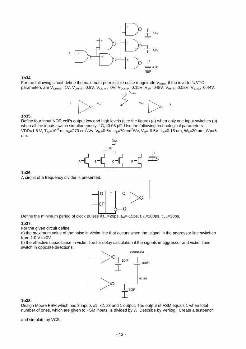
- 43 -
1b34. For the following circuit define the maximum permissible noise magnitude Vnoise, if the inverter’s VTC parameters are VOHnom=1V, VOHmin=0.9V, VOLnom=0V, VOLmax=0.15V, VSP=048V, VIHmin=0.58V, VILmax=0.44V.
1b35. Define four input NOR cell’s output low and high levels (see the figure) (a) when only one input switches (b) when all the inputs switch simultaneously if CL=0.05 pF. Use the following technological parameters
VDD=1.8 V, Tox=10-8
m, n=270 cm2/Vv, Vtn=0.5V, p=70 cm
2/Vv, Vtp=-0.5V, Ln=0.18 um, Wn=20 um, Wp=5
um.
1b36. A circuit of a frequency divider is presented.
Define the minimum period of clock pulses if tsu=20ps, thd=-15ps, tc2q=100ps, tpinv=30ps.
1b37. For the given circuit define: a) the maximum value of the noise in victim line that occurs when the signal in the aggressor line switches from 1.0 V to 0V. b) the effective capacitance in victim line for delay calculation if the signals in aggressor and victim lines switch in opposite directions.
1b38. Design Moore FSM which has 3 inputs x1, x2, x3 and 1 output. The output of FSM equals 1 when total number of ones, which are given to FSM inputs, is divided by 7. Describe by Verilog. Create a testbench and simulate by VCS.
4.5C
A C
y
y z
z
z
4.5C
4.5C
B
x Vout1 Vin2
1
Vnoise
y
F
CL D C B A
VDD
60fF
100fF
50fF
aggressor
victim
Q D
CP
T
Q
- 44 -
1b39. Describe by Verilog 5-bit polynomial counter (LFSR). In feedback circuit d(x) = 1+ x
3 +x
5 is polynomial. The
counter has 10000 initial state asynchronous preset input. The shift of information is realized by positive edge of clock signal. Describe by Verilog. Create a testbench and simulate using VCS.
1b40. Define the minimum H distance between two rows of cells which is necessary for routing of two-layer co-perpendicular routing of a, b, c, d, e nets if the minimum permissible size between interconnects width and space is 0,1 um, and the minimum distance between interconnects and 0,2 um.
1b41. Switching block with 4 pins (1, 2, 3, 4) is shown in the figure. It consists of 4 NMOS and 2 PMOS transistors. What kind of logic level signals (0 or 1) should be given to each gate of T1-T6 transistors to provide: a) Simultaneous signal transfer from pin 1 to 3 and from pin 2 to 4; b) Simultaneous signal transfer from pin 1 to 4 and from pin 2 to 3;
1b42. Two modules (M1 and M2) are connected with 5 interconnects (l1-l5) and 4 programmable vias (1-4). Construct interconnect’s R, C equivalent circuit and calculate the delay in the transmission line connecting two modules, if given: Each transmission line capacitance of interconnect equals 100 fF. Each programmable contact resistance equals 1 Ohm. Ignore ohmic resistances of interconnects and contacts as well as the capacitances of programmable vias.
1b43. Calculate faultness probability of IC consisting of 7 blocks if their connection, according to reliability, has the following view. Given P1=0,5; P2=0,6; P3=0,8; P4=0,4.
a e a d c
a b b e
d
c
H
2
T2
T3
T4
T5
T6
T1
3
4
1
M1
M2
l3
l1
l5 l4
Interconnects
4
1
3
2
l2
Programmable vias
P1
P2 P3
P1 P4
P4
FSM x1 x2 x3
y
- 45 -
1b44.
Using the following parameters, define the current through series connected transistors. Kp’=25
mkA/V2, VT0=1.0V, =0.39V
1/2, 2|F|=0.6V, W/L=1.
Consider the body bias effect. Several iterations will be needed for the solution.
1b45. The first inverter of the presented buffer is of minimal size, input capacitance is C in=10 fF, delay 70 ps. The load capacitance of the buffer is CL=20 pf. a) Define the sizes of the other two inverters with respect to the minimal one. Use the condition to get
minimum delay, consider that input capacitances are proportional to sizes. b) Add any number of inverters to get minimum delay. Define the total delay. c) Define the power consumption of the circuit if the supply voltage is 2.5V, operating frequency 200 MHz.
1b46. Design a CMOS cell, implementing F = AB + AC + BC function. Choose a transistor sizes such that NMOS and PMOS net resistances are equal to the minimal size inverter’s resistances. Consider 2k’p = k’n. For what input combinations will the best and the worst resistances be obtained?
1b47. A cell with transistor switches is presented in the figure. a) What function does the cell implement? Show the truth
table. b) Considering inputs 0 and 2.5V, choose PMOS transistor’s
sizes such that VOL = 0.3V. Consider 2k’p = k’n and |Vtp|= Vtn=0.5V, for NMOS transistors W/L=1.5um/0.25um.
c) Will the cell continue to operate correctly if a PMOS transistor is removed? Does the PMOS transistor implement any helpful function?
1b48.
In the presented figure Cx = 50 fF, M1 transistor’s W/L =
0.375um/0.375um, M2 transistor’s W/L= 0.375um/0.25um.
Note that the inverter does not switch until the input Vx
voltage reaches VDD/2. VDD = 2.5V (W/L)3 = 1.5um/0.25um (W/L)4 = 0.5um/0.25um kn’ = 115mkA/V
2, kp’ = -30mkA/V
2
VtN = 0.43V, VtP = -0.4V a) How long will it take for M1 transistor to move x node from
2.5V to 1.25V if Vin = 0V, VB= 2.5V? b) How long will it take for M2 transistor to move x node from
0V to 1.25V if Vin = 2.5V, VB= 2.5V? c) What is the minimum value of VB voltage for Vx=1.25V
when Vin = 0V?
5V ID
5V
CL Cin ?
1 x x
Cx
VDD
VDD
VSS
Vin Vout
B M2
M3
M4
X
M1
VDD
Y
VSS
A
B
- 46 -
1b49. For the figure shown below in a MOS inverter, consider that all transistor bulks are connected to the ground and the IN input changes from 0V to 2.5V. a) Get the expression to compute x node’s voltage
considering =0.5, 2|f|=0.6V, Vt0=0.5V, VDD=2.5V.
b) Considering =0, define the operating modes of M2.
c) Considering =0, define the output value when Vin =0V.
d) Considering =0, get the expression of inverter’s switching point voltage (VSP) (in the switching point VIN= VOUT). Consider M1, M2 and M3 transistor sizes (W/L)1, (W/L)2 and (W/L)3 respectively. Define changing limits of VSP when (1) (W/L)1 >> (W/L)2, (2) (W/L)2 >> (W/L)1.
1b50. For the given inverter (W/L)1=5um/0.25um, (W/L)2=4um/0.25um, kn = 120uA/V
2, kp = 30uA/V
2, VtN = 0.5V,
VtP = -0.4V, VDD=2.5V. a) VOL and VOH b) VSP
1b51.
Design a cascade differential voltage switching logic cell which is described by the equation . Use minimum number of transistors. Consider that normal and inverted values of inputs are
available.
1b52. A circuit of a flip-flop with combined logic is shown. Define for which values of S1, S2, S3 signals this circuit will operate as:
• Positive edge-triggered D-flip-flop with synchronous reset • Positive edge-triggered T- flip-flop with synchronous reset • D-latch •Transfer of input data to output
1b53. Define what input binary sequence detector the given circuit is. The beginning of the following sequence can be the end of the previous one.
1b54. Using three- and four-bit Johnson counters (one of them having odd number of states), construct a counter with 42 states. Construct a decoder that will decode every 6
th state starting from 0.
VDD
Vin
M1
M2
Vout
VSS
0
1
D
Clk
S1
Data
0
1
0
1
0 0
1
0
1
Clk
S2
S3
reset
Out
“1”
D
Clk
D
Clk
x
y
Rese
t Clk
d1 q1 q2
d2
Vin
Vout
M1
M2
M3
X

- 47 -
1b55. It is required to design an arbiter circuit that performs the following function: allows availability to four devices into the general resource of the given system. At any time only one device can use the resource. Each device creates a request which is given to the arbiter input by clock: The FSM for each device generates an access to permission signal – grant. The requests are processed as per priority. After processing the request from some device, the device removes the request and the FSM comes to its initial state. The system also has an additional input that defines the priorities of requests. If direction=0, the highest priority is r0 request, then r1, r2 and r3. And if direction=1, the priorities have opposite order r3,r2,r1,r0.
1. Devise transition graph of arbiter states 2. Describe the FSM in Verilog.
1b56. Suppose there is a given "data_in" signal with one hot logic vector of 8-bit of width. And the goal is to calculate the encoded decimal value of the bit index having value of 1'b1 (the following 'case' statements show the required logic).
input [7:0] data_in;
output [3:0] data_out;
casez(data_in) //data_in can have only one 1 at a time
8'b???????1: data_out = 3'd0;
8'b??????10: data_out = 3'd1;
8'b?????100: data_out = 3'd2;
8'b????1000: data_out = 3'd3;
8'b???10000: data_out = 3'd4;
8'b??100000: data_out = 3'd5;
8'b?1000000: data_out = 3'd6;
8'b10000000: data_out = 3'd7;
default: data_out = 3'd0;
endcase
Note, 'one hot logic vector' means that this vector will have only one. 1'b1 value in its bits. E.g.: 0001 0010 0100 1000 Provide an optimal gate-level logic equivalent to this case statement (using only logical AND, OR and NOT gates). The answer may be provided in either VerilogHDL or schematic drawing interpretation. a) Provide the gate level derivation logic for data_out[0]. b) Provide the gate level derivation logic for data_out[1]. c) Provide the gate level derivation logic for data_out[2].
1b57. Consider the implementation of a 3-input OR gate shown in the figure below. Assume there are 3 inputs A, B, and C where P(A=1)=0.5, P(B=1)=0.2, P(C=1)=0.1. For a static CMOS implementation of this circuit: a) What is the best order to place these inputs to minimize power consumption? b) What is the worst order? c) What is the activity factor at the internal node (X) in these cases?
1b58. Derive the truth table, state transition graph, and output transition probabilities for a three-input XOR gate with independent, a) Identically distributed, uniform white-noise inputs. b) P(A=1)=0.2, P(B=1)=0.4, P(C=1)=0.6.
1b59. Implement the equation X=((!A+!B)(!C+!D+!E)+!F)!G using complementary CMOS. Size the devices such that the output resistance is the same as that of an inverter with an NMOS W/L = 2 and PMOS W/L = 6.
In1
In2
X
In3

- 48 -
1b60. Determine the power dissipation in the circuit, if VDD=1V, the input frequency is 800 MHz, input and output capacitances of inverters are Cin=15fF, Cout=10fF, the load capacitance is Cload= 100fF.
1b61. Determine the switching point voltage of a CMOS NAND2 cell: (W/L)n=14, (W/L)p=12 and inputs switch
simultaneously, VDD=3.3 V, Tox=1.5*10-8
m, n=550 cm2/Vs, Vtn=0.7 V, p=180 cm
2/Vs, Vtp=-0.8 V.
1b62. Calculate the 50% level rise delay at the end of a 500um x 0.5um wire. The sheet resistance is 0.08 Ohm/sq, overlap capacitance is 30 aF/um
2, fridge capacitance is 40 aF/u, the internal resistance of the signal source
is 100 Ohm, the load capacitance at the end of wire can be neglected. a) Use lamped parameters. b) Use distributed parameters. c) Use ladder model dividing the wire into 10um pieces.
1b63. Implement required logic satisfying the functionality shown by waveform drawing. Use logic OR, AND and NOT gates and/or D-flip-flops as needed. The implementation may be done in either principle schematic, or Verilog HDL, or VHDL formats (syntax accuracy is not required).
clock input_signal output_signal
1b64. Implement required logic satisfying the functionality shown by waveform drawing. Use logic OR, AND and NOT gates and/or D-flip-flops as needed. The implementation may be done in either principle schematic, or Verilog HDL, or VHDL formats (syntax accuracy is not required).
clock
input_signal output_signal
1b65. Implement required logic satisfying the functionality shown by waveform drawing. Use logic OR, AND and NOT gates and/or D-flip-flops as needed. The implementation may be done in either principle schematic, or Verilog HDL, or VHDL formats (syntax accuracy is not required).
clock input_signal output_signal
1b66. Implement required logic satisfying the functionality shown by waveform drawing. Use logic OR, AND and NOT gates and/or D-flip-flops as needed. The implementation may be done in either principle schematic, or Verilog HDL, or VHDL formats (syntax accuracy is not required).
clock
input_signal
output_signal
Vin
21
Cload
Vout
2
Vin1 Vout1

- 49 -
1b67. Design modulo-3 binary counter. Sequence of states 0,1,2,0,1,2,… . Use JK-flip-flop. 1b68. Mealy FSM is given with the following table. It has 3 states, input alphabet is X={0,1}, output alphabet is Y={0,1}, internal variables: q1, q2.
Describe the FSM on Verilog.
1b69. Compose Verilog description of synthesized model of N-bit binary reverse counter with Up and Down inputs. If Up=1 the content of counter increases by 1, the Down=1 content of counter decreases by 1. If the state of Up=Down=0 counter does not change, Up=Down=1 input is prohibited. The counter changes its state at negative edge of the clock. The reset is synchronous. N=8. 1b70. By Verilog describe 7-bit polynomial counter (LFSR). In feedback circuit d(x) = 1+ x
6+x
7 is polynomial. The
data are loaded asynchronously from data input by high level of load signal. 1b71. By Verilog describe the ALU that performs the operations, mentioned in the table. All logic operations are bitwise.
1b72. Develop a circuit of addition four 4-bit numbers using CSA. Define carry propagation delay for the worst case. 1b73. Develop a scheme of matrix multiplier for unsigned 4-bit numbers. Define the carry signal propagation delay in the worst case. 1b74. Given below is a state transition diagram in which the states are already coded. Draw the circuit implementation of this automation.
1b75. Determine the State-Output-Table for the given State-Transition-Graph. Which states are unreachable?
State-Transition-Graph:
00 10
01
0/0
1/0 1/0
1/0 0/1
0/0
S
1
S
4
S
3
S
2
1/0
0/1
0/0 0/0 1/1 1/1
1/1
0/1
Current state Next state, Y
X=0 X=1
q1 q2 q1 q2, Y q1 q2, Y
0 0 0 1, 0 1 0, 1
0 1 1 0, 1 0 0, 1
1 0 0 0, 1 0 1, 1
Function code (F) Function
0 0 0 А & B
0 0 1 A | B
0 1 0 A+ B
0 1 1 Not used
1 0 0 A B
1 0 1 A – B
1 1 0 A OR ~B
1 1 1 ~ A
x=0 x=1
S1
S2
S3
S4
А
B
Y
F
ALU
- 50 -
1b76. A logic function f(x1,x2,x3,x4,x5) is decomposed into a multilevel function z(y(x1,x2,x3),x4,x5):
5454 xxy+xyx=z
212132 xx+xx+xx=y
This decomposed logic function has to be realized using two lookup tables (LUTs), which are connected as shown below. Determine the logic values that have to be stored in the LUTs to implement the given function. The logic values are equal to the output of the LUT for the given row of input values.
1b77.
a) Synthesize CMOS circuitry that provides output D) or (C and B) and(A F ;
b) Define dimensions of all transistors to obtain rising and falling times at output to be at most (worst case) equal to those that explores a unit inverter in the same technology (assume dimension of the unit inverter as
Wp/Lp=3*6/2 and Wn/Ln=6l/2l).
1b78. a) Find minimal possible delay on path A - D. b) Define dimensions of transistors in order to achieve minimal delay for the circuitry in the figure. X and Y denote multiplication factors of input capacitances in terms of capacitance of an unit nMOS (nMOS with minimal dimensions). Unit inverter input capacitance for given technology is assumed to be C inv=3C, (2C from pMOS and 1C from nMOS). Give the transistor widths in terms of Wno of the unit nMOS.
Cell INV NAND2 NANDn NOR2 NORn
Parasitic delay (p) 1 2 n 2 n
Logical effort (g) 1 4/3 (n+2)/3 5/3 (2n+1)/3
x*c 1 2 3 4
5
NOR4
x*c 1 2 3 4
5
NOR4
x*c 1 2 3 4
5
NOR4
x*c 1 2 3 4
5
NOR4
4 1
3 y*c
NAND3 2
27 C
27 C
4 1
3 y*c
NAND3
2 D
G
4 1
3 y*c
NAND3 2
27 C
2
3 1
10*c NAND2
A C
G B
G
000 001 010 011 100 101 110 111
z
000 001 010 011 100 101 110 111
y
X1
X2 X3 X4
X5
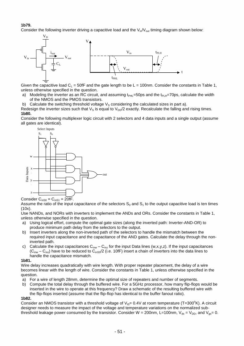
- 51 -
1b79. Consider the following inverter driving a capacitive load and the Vin/Vout timing diagram shown below:
Given the capacitive load CL = 50fF and the gate length to be L = 100nm. Consider the constants in Table 1, unless otherwise specified in the question. a) Modeling the inverter as an RC circuit, and assuming tPHL=50ps and the tPLH=70ps, calculate the width
of the NMOS and the PMOS transistors. b) Calculate the switching threshold voltage VS considering the calculated sizes in part a).
Redesign the inverter sizes such that VS is equal to VDD/2 exactly. Recalculate the falling and rising times. 1b80. Consider the following multiplexer logic circuit with 2 selectors and 4 data inputs and a single output (assume all gates are identical).
Consider CinS0 = CinS1 = 20fF. Assume the ratio of the input capacitance of the selectors S0 and S1 to the output capacitive load is ten times (10x). Use NANDs, and NORs with inverters to implement the ANDs and ORs. Consider the constants in Table 1, unless otherwise specified in the question. a) Using logical effort, compute the optimal gate sizes (along the inverted path: Inverter-AND-OR) to
produce minimum path delay from the selectors to the output. b) Insert inverters along the non-inverted path of the selectors to handle the mismatch between the
required input capacitance and the capacitance of the AND gates. Calculate the delay through the non-inverted path.
c) Calculate the input capacitances Cinw – Cinz for the input Data lines (w,x,y,z). If the input capacitances (Cinw – Cinz) have to be reduced to CinS0/2 (i.e. 10fF) insert a chain of inverters into the data lines to handle the capacitance mismatch.
1b81. Wire delay increases quadratically with wire length. With proper repeater placement, the delay of a wire becomes linear with the length of wire. Consider the constants in Table 1, unless otherwise specified in the question. a) For a wire of length 28mm, determine the optimal size of repeaters and number of segments. b) Compute the total delay through the buffered wire. For a 5GHz processor, how many flip-flops would be
inserted in the wire to operate at this frequency? Draw a schematic of the resulting buffered wire with the flip-flops inserted (assume that the flip-flop has identical to the buffer fanout ratio).
1b82. Consider an NMOS transistor with a threshold voltage of Vt0= 0.4V at room temperature (T=300
oK). A circuit
designer needs to measure the impact of the voltage and temperature variations on the normalized sub-threshold leakage power consumed by the transistor. Consider W = 200nm, L=100nm, Vds = VDD, and Vgs= 0.
S1 S0
out
w
x
y
z
Select Inputs
Dat
a In
puts
V
Vin tPLH
tPHL
Vout t
iout
Vout Vin
VD
D
CL
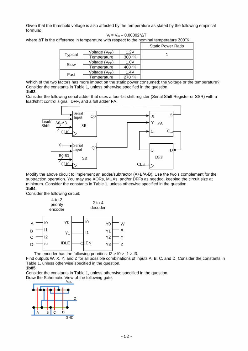
- 52 -
Given that the threshold voltage is also affected by the temperature as stated by the following empirical formula:
Vt = Vt0 – 0.00002*ΔT where ΔT is the difference in temperature with respect to the nominal temperature 300
oK.
Static Power Ratio
Typical Voltage (VDD) 1.2V
1 Temperature 300
oK
Slow Voltage (VDD) 1.0V
Temperature 400
oK
Fast Voltage (VDD) 1.4V
Temperature 270
oK
Which of the two factors has more impact on the static power consumed: the voltage or the temperature? Consider the constants in Table 1, unless otherwise specified in the question. 1b83. Consider the following serial adder that uses a four-bit shift register (Serial Shift Register or SSR) with a load/shift control signal, DFF, and a full adder FA.
Modify the above circuit to implement an adder/subtractor (A+B/A-B). Use the two’s complement for the subtraction operation. You may use XORs, MUXs, and/or DFFs as needed, keeping the circuit size at minimum. Consider the constants in Table 1, unless otherwise specified in the question. 1b84. Consider the following circuit:
The encoder has the following priorities: I2 > I0 > I1 > I3. Find outputs W, X, Y, and Z for all possible combinations of inputs A, B, C, and D. Consider the constants in Table 1, unless otherwise specified in the question. 1b85. Consider the constants in Table 1, unless otherwise specified in the question. Draw the Schematic View of the following gate:
A
B
C
D
W
X
Y
Z IDLE
I0
I1
EN
Y0
Y1
I0
I1
I2
I3
Y0
Y1
Y2
Y3
4-to-2 priority
encoder
2-to-4 decoder
VDD
GND
Z
A B C D
Serial Input
Serial Input Q0
Q0 Q D
X
Y
Ci
n Cout
FA
S
DFF SR
SR
CLK
CLK CLK
Load/ Shift
A0-A3
B0-B3
0

- 53 -
1b86. Consider the following two gates:
For each of the two gates: a) Calculate the proper sizing of the PMOS and NMOS transistors for the worst-case delay scenario, such
that the pull-up and pull-down equivalent sizes are equal to those of an inverter with sizes 2W, and W (for PMOS and NMOS respectively).
b) Calculate the input capacitance (gate capacitance), of input A, B, C and D based on the sizes calculated in a), (W = Wn= 200nm).
c) Calculate the self-capacitance based on the transistor sizes in a), (W = Wn= 200nm). Consider the constants in Table 1, unless otherwise specified in the question.
Table 1 Data used 1b79-1b86 problems
1b87. Design a two directional three-bit counter with the following functionality. The counter is changing its value on each positive edge of the clock. The counter's reset value is 0. After reset the counter is being incremented to value of decimal 4, then decremented back to 0, then incremented to 2, then decremented back to 0, and continue this defined whole sequence forever, i.e.: reset, 0,1,2,3,4,3,2,1,0,1,2,1,0,1,2,3,4,3,2,1,0,1,2,1,0....... The implementation may be done in any of hardware description languages (HDL) and the syntax accuracy is not required. 1b88. Design a two directional three-bit counter with the following functionality. The counter is changing its value on each positive edge of the clock. The counter's reset value is 0. After reset the counter is being incremented for two steps, then is decremented back for one step, and continues this defined whole sequence forever, i.e.: reset,0,1,2,1,2,3,2,3,4,3,4,5,4,5,6,5,6,7,6,7,0,7,0,1,0,1,2,1...... The implementation may be done in any of hardware description languages (HDL) and the syntax accuracy is not required. 1b89. Design a three-bit increment counter with the following functionality. The counter is changing its value on each positive edge of the clock. The counter's reset value is 0. After reset the counter is being incremented to value of decimal 1, then at next step it jumps back to value of 0. Then step by step increments to 2 and again jumps back to 0. Then step by step increments to 3 and again jumps back to 0. After the reaching to value of 4 and jumping to 0 the counter should start from the beginning and continue this defined whole sequence forever, i.e.: reset,0,1,0,1,2,0,1,2,3,0,1,2,3,4,0,1,0,1,2,0,1,2,3,0,1,2,3,4,0....... The implementation may be done in any of hardware description languages (HDL) and the syntax accuracy is not required. 1b90. Design a two directional three-bit counter with the following functionality. The counter is changing its value on each positive edge of the clock. The counter's reset value is 0. After reset the counter is being incremented for five steps, then is decremented back for two steps, and continues this defined whole sequence forever, i.e.:
D
VDD
Y
B
A
A
C
C
D
B
E
D
E D
C
VDD
F
A
A
B
B
C
(1) (2)
VDD=1.2V |VTP|=VTN = 0.4V Ecn = 6V/m Ecp = 24 V/m
vsat = 8*106 cm/sec 2|F| = 0.88V en =270 cm2/V-sec ep =70 cm2/V-sec
= 0.2(V1/2
) λ=0.01V-1
q =1.6*10-19
C n =1.4
T = 300 oK (27
oC) k = 1.38*10
-23 J/
oK o = 8.85*10
-14 F/cm ox = 3.970
L= 100nm xd =20nm Reqn = 12.5 kΩ/☐ Reqp = 30.0 kΩ/☐
Cox = 1.6x10⁻⁶
F/cm2 Cg = 2 fF/um Ceff = 1fF/um Cu = 1.7-cm
Wint = 0.17m Tint = 0.8m Cint = 0.2fF/m Voffset = 0
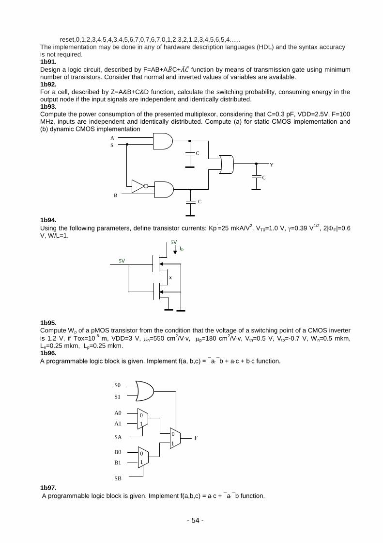
- 54 -
reset,0,1,2,3,4,5,4,3,4,5,6,7,0,7,6,7,0,1,2,3,2,1,2,3,4,5,6,5,4...... The implementation may be done in any of hardware description languages (HDL) and the syntax accuracy is not required. 1b91. Design a logic circuit, described by F=AB+A C+ function by means of transmission gate using minimum number of transistors. Consider that normal and inverted values of variables are available. 1b92. For a cell, described by Z=A&B+C&D function, calculate the switching probability, consuming energy in the output node if the input signals are independent and identically distributed. 1b93. Compute the power consumption of the presented multiplexor, considering that C=0.3 pF, VDD=2.5V, F=100 MHz, inputs are independent and identically distributed. Compute (a) for static CMOS implementation and (b) dynamic CMOS implementation
1b94. Using the following parameters, define transistor currents: Kp
’=25 mkA/V
2, VT0=1.0 V, =0.39 V
1/2, 2|F|=0.6
V, W/L=1.
1b95. Compute Wp of a pMOS transistor from the condition that the voltage of a switching point of a CMOS inverter
is 1.2 V, if Tox=10-8
m, VDD=3 V, n=550 cm2/Vv, p=180 cm
2/Vv, Vtn=0.5 V, Vtp=-0.7 V, Wn=0.5 mkm,
Ln=0.25 mkm, Lp=0.25 mkm. 1b96. A programmable logic block is given. Implement f(а, b,c) = ab + ac + bc function.
1b97. A programmable logic block is given. Implement f(a,b,c) = ac + ab function.
F
A0
A1
B0
0 B1
SA
S0
S1
SB
0
1
1
0
1
0
5V
ID
5V
x
A
S
B
Y
C
C
C
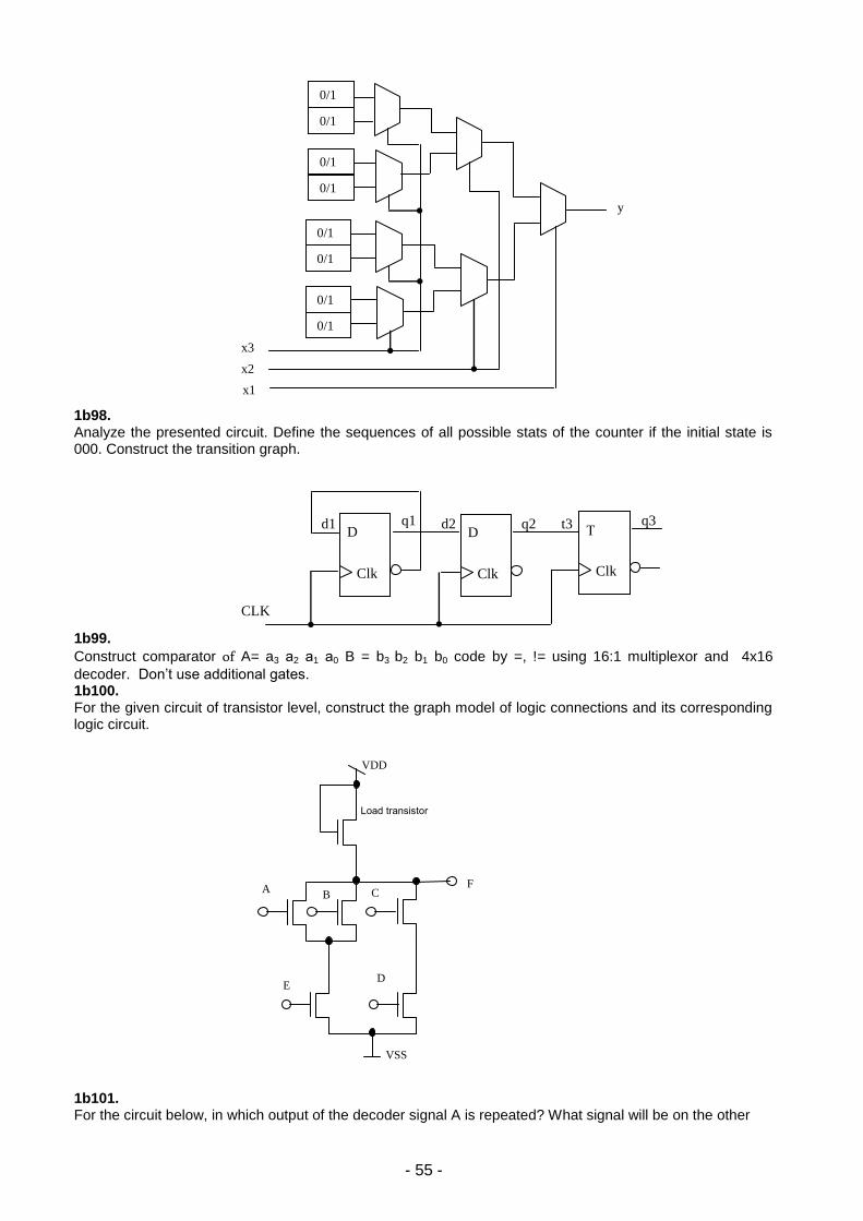
- 55 -
1b98. Analyze the presented circuit. Define the sequences of all possible stats of the counter if the initial state is 000. Construct the transition graph.
1b99. Construct comparator of A= a3 а2 а1 а0 B = b3 b2 b1 b0 code by =, != using 16:1 multiplexor and 4x16
decoder. Don’t use additional gates. 1b100. For the given circuit of transistor level, construct the graph model of logic connections and its corresponding logic circuit.
1b101. For the circuit below, in which output of the decoder signal A is repeated? What signal will be on the other
Load transistor
VDD
D
C B A
VSS
E
F
D
Clk
D
Clk
Т
Clk
CLK
q1 q2 q3 t3 d2 d1
0/1
0/1
0/1
0/1
0/1
0/1
0/1
0/1
x3
x2
x1
y
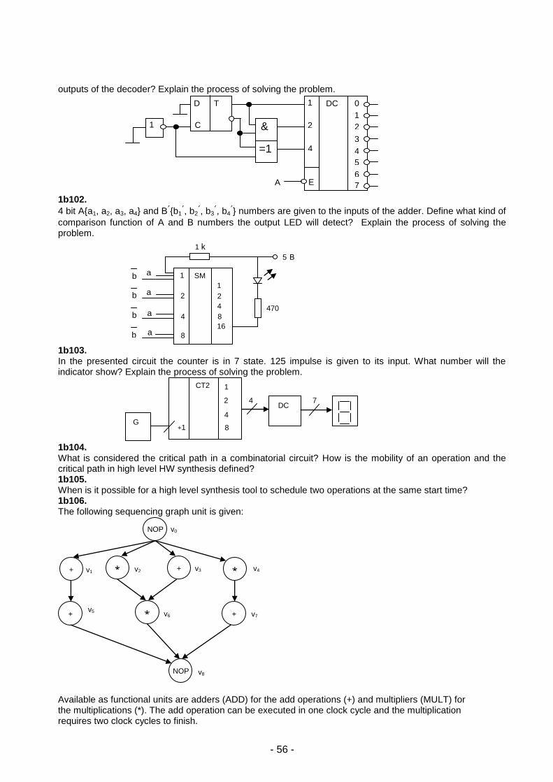
- 56 -
outputs of the decoder? Explain the process of solving the problem.
1b102. 4 bit A{a1, a2, a3, a4} and B՛{b1՛, b2՛, b3՛, b4՛} numbers are given to the inputs of the adder. Define what kind of
comparison function of A and B numbers the output LED will detect? Explain the process of solving the problem.
1b103. In the presented circuit the counter is in 7 state. 125 impulse is given to its input. What number will the indicator show? Explain the process of solving the problem.
1b104. What is considered the critical path in a combinatorial circuit? How is the mobility of an operation and the critical path in high level HW synthesis defined? 1b105. When is it possible for a high level synthesis tool to schedule two operations at the same start time? 1b106. The following sequencing graph unit is given:
Available as functional units are adders (ADD) for the add operations (+) and multipliers (MULT) for the multiplications (*). The add operation can be executed in one clock cycle and the multiplication requires two clock cycles to finish.
NOP v0
+
+
*
+
+ *
*
v1 v2 v3 v4
v5 v6 v7
NOP v8
CT2
+1
1
8
2
4
4 7
G
DC
a
1 b
1 b
2
b
3
b
4
a
2
a
3 a
4
1 k
5 В
470
SM 1
1
2 2
4
4
8
8
16
1
D T
C &
=1
A
E
1
2
4
DC 0
1
2
3
4
5
6
7
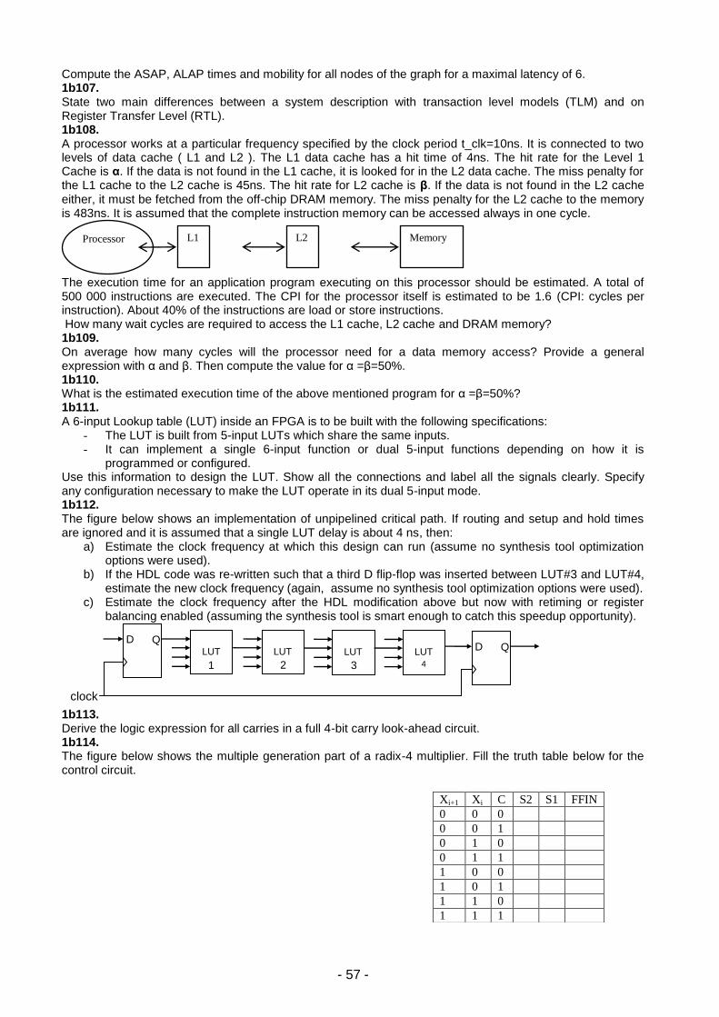
- 57 -
Compute the ASAP, ALAP times and mobility for all nodes of the graph for a maximal latency of 6. 1b107. State two main differences between a system description with transaction level models (TLM) and on Register Transfer Level (RTL). 1b108. A processor works at a particular frequency specified by the clock period t_clk=10ns. It is connected to two levels of data cache ( L1 and L2 ). The L1 data cache has a hit time of 4ns. The hit rate for the Level 1 Cache is α. If the data is not found in the L1 cache, it is looked for in the L2 data cache. The miss penalty for the L1 cache to the L2 cache is 45ns. The hit rate for L2 cache is β. If the data is not found in the L2 cache either, it must be fetched from the off-chip DRAM memory. The miss penalty for the L2 cache to the memory is 483ns. It is assumed that the complete instruction memory can be accessed always in one cycle.
The execution time for an application program executing on this processor should be estimated. A total of 500 000 instructions are executed. The CPI for the processor itself is estimated to be 1.6 (CPI: cycles per instruction). About 40% of the instructions are load or store instructions. How many wait cycles are required to access the L1 cache, L2 cache and DRAM memory? 1b109. On average how many cycles will the processor need for a data memory access? Provide a general expression with α and β. Then compute the value for α =β=50%. 1b110. What is the estimated execution time of the above mentioned program for α =β=50%? 1b111. A 6-input Lookup table (LUT) inside an FPGA is to be built with the following specifications:
- The LUT is built from 5-input LUTs which share the same inputs. - It can implement a single 6-input function or dual 5-input functions depending on how it is
programmed or configured. Use this information to design the LUT. Show all the connections and label all the signals clearly. Specify any configuration necessary to make the LUT operate in its dual 5-input mode. 1b112. The figure below shows an implementation of unpipelined critical path. If routing and setup and hold times are ignored and it is assumed that a single LUT delay is about 4 ns, then:
a) Estimate the clock frequency at which this design can run (assume no synthesis tool optimization options were used).
b) If the HDL code was re-written such that a third D flip-flop was inserted between LUT#3 and LUT#4, estimate the new clock frequency (again, assume no synthesis tool optimization options were used).
c) Estimate the clock frequency after the HDL modification above but now with retiming or register balancing enabled (assuming the synthesis tool is smart enough to catch this speedup opportunity).
1b113. Derive the logic expression for all carries in a full 4-bit carry look-ahead circuit. 1b114. The figure below shows the multiple generation part of a radix-4 multiplier. Fill the truth table below for the control circuit.
Xi+1 Xi C S2 S1 FFIN
0 0 0
0 0 1
0 1 0
0 1 1
1 0 0
1 0 1
1 1 0
1 1 1
clock
D Q
LUT
1
LUT
2
LUT
3
LUT
4
D Q
Processor L1 L2 Memory
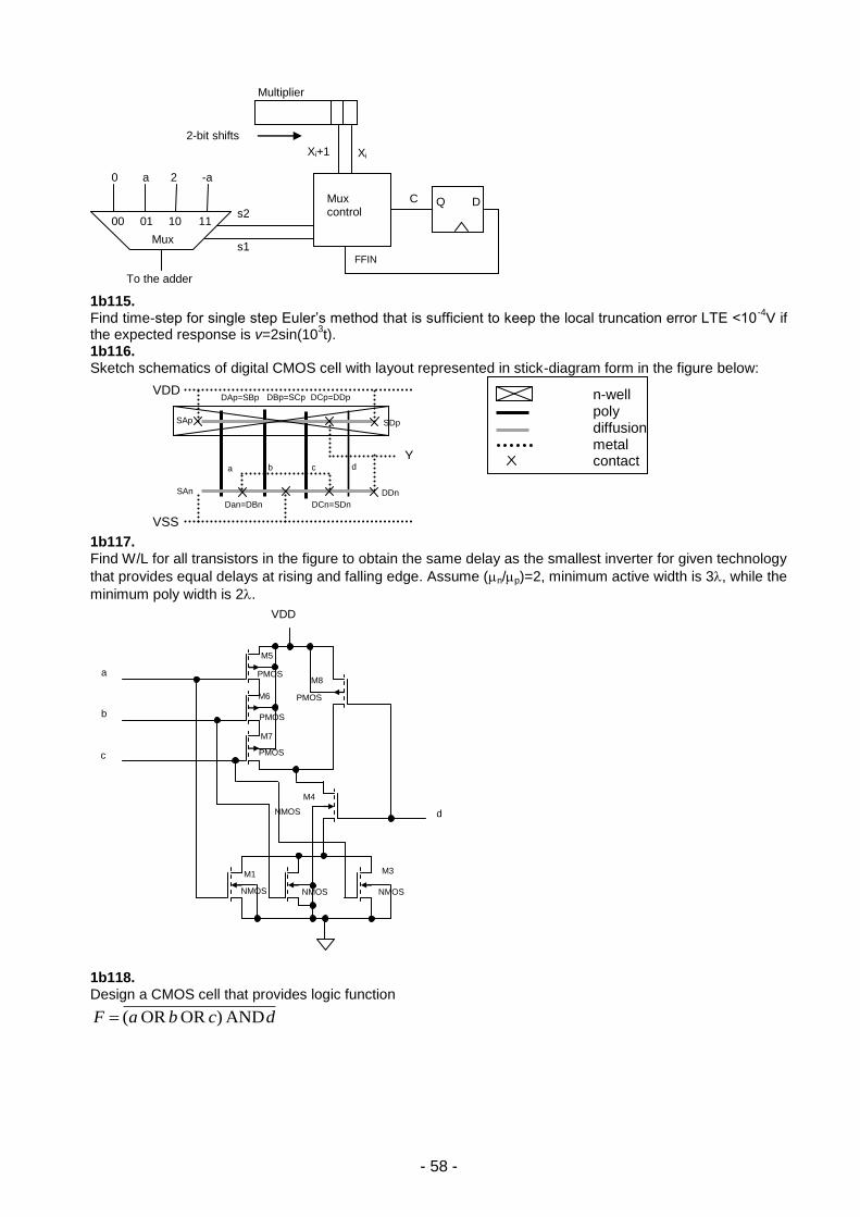
- 58 -
1b115. Find time-step for single step Euler’s method that is sufficient to keep the local truncation error LTE <10
-4V if
the expected response is v=2sin(103t).
1b116. Sketch schematics of digital CMOS cell with layout represented in stick-diagram form in the figure below:
1b117. Find W/L for all transistors in the figure to obtain the same delay as the smallest inverter for given technology
that provides equal delays at rising and falling edge. Assume (n/p)=2, minimum active width is 3, while the
minimum poly width is 2.
1b118. Design a CMOS cell that provides logic function
dcbaF AND ) OR OR (
a
b
c
d
VDD
M1 M3
NMOS NMOS NMOS
M5
M6
M7
M8 PMOS
PMOS
PMOS
PMOS
M4
NMOS
VDD
VSS
SAp
SAn
a b c d Y
SDp
DDn
Dan=DBn
DAp=SBp DBp=SCp DCp=DDp
DCn=SDn
n-well poly diffusion metal contact
0 a 2
a -a
00 01 10 11
Mux
To the adder
2-bit shifts
Multiplier
Xi+1 Xi
s2
s1
Mux control
C Q D
FFIN
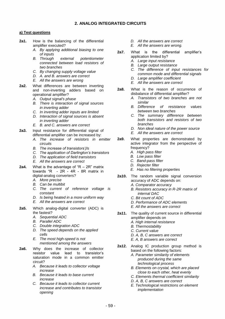
- 59 -
2. ANALOG INTEGRATED CIRCUITS
a) Test questions 2a1. How is the balancing of the differential
amplifier executed? A. By applying additional biasing to one
of inputs B. Through external potentiometer
connected between load resistors of two branches
C. By changing supply voltage value D. A. and B. answers are correct E. All the answers are wrong
2a2. What differences are between inverting and non-inverting adders based on operational amplifier? A. Output signal's phase B. There is interaction of signal sources
in inverting adder C. In inverting adder inputs are limited D. Interaction of signal sources is absent
in inverting adder E. B. and C. answers are correct
2a3. Input resistance for differential signal of differential amplifier can be increased by: A. The increase of resistors in emitter
circuits
B. The increase of transistors’s C. The application of Darlington’s transistors D. The application of field transistors E. All the answers are correct
2a4. What is the advantage of “R – 2R” matrix towards “R 2R 4R 8R matrix in digital-analog converters? A. More precise B. Can be multibit C. The current of reference voltage is
constant D. Is being heated in a more uniform way E. All the answers are correct
2a5. Which analog-digital converter (ADC) is the fastest? A. Sequential ADC B. Parallel ADC C. Double integration ADC D. The speed depends on the applied
cells E. The most high-speed is not
mentioned among the answers
2a6. Why does the increase of collector resistor value lead to transistor’s saturation mode in a common emitter circuit? A. Because it leads to collector voltage
increase B. Because it leads to base current
increase C. Because it leads to collector current
increase and contributes to transistor opening
D. All the answers are correct E. All the answers are wrong.
2a7. What is the differential amplifier’s application limited by? A. Large input resistance B. Large output resistance C. The difference of input resistances for
common mode and differential signals D. Large amplifier coefficient E. All the answers are correct
2a8. What is the reason of occurrence of disbalance of differential amplifier? A. Transistors of two branches are not
similar B. Difference of resistance values
between two branches C. The summary difference between
both transistors and resistors of two branches
D. Non ideal nature of the power source E. All the answers are correct
2a9. What properties are demonstrated by active integrator from the perspective of frequency? A. High pass filter B. Low pass filter C. Band-pass filter D. Rejecter filter E. Has no filtering properties
2a10. The random variable signal conversion accuracy of ADC depends on: A. Comparator accuracy B. Resistors accuracy in R-2R matrix of
internal DAC C. Bit count of ADC D. Performance of ADC elements E. All the answers are correct
2a11. The quality of current source in differential amplifier depends on A. High internal resistance B. Thermostability C. Current value D. A, B, C answers are correct E. A, B answers are correct
2a12. Analog IC production group method is based on the following factors: A. Parameter similarity of elements
produced during the same technological process
B. Elements on crystal, which are placed close to each other, heat evenly
C. Elements thermal coefficient similarity D. A, B, C answers are correct E. Technological restrictions on element
implementation

- 60 -
2a13. What is the minimum value of the resistance of OpAmp negative feedback limited by? A. Ku=1 request B. Thermal instability of input current C. Permissible minimum value of
resistance of OpAmp output load D. No limitation E. All the answers are wrong
2a14. In voltage stabilizer by OpAmp application why is the feedback given to the inverse input not from OpAmp output, but from the output of output emitter repeater A. To fade the loading of OpAmp B. To fade stabilitron current given to the
direct input C. To compensate thermal instability of
the output emitter repeater D. To increase amplifier’s coefficient of
OpAmp E. All the answers are correct
2a15. What factors is the redundancy principle of analog microcircuitry based on? A. Technological restrictions of element
preparation B. On those elements of the circuit which
are not possible to carry out in crystal or occupy too much area, are substituted by multielement node which implements the same function.
C. A. and B. answers are correct D. On placing redundant elements on
crystal area E. Minimization of the number of circuit
elements
2a16. Why does not the emitter oscillate the voltage? A. Because the output voltage must
always be smaller than the one of the input for open state of the transistor
B. Because it is not possible to increase large nominal resistance in emitter circuit
C. Because the output signal is taken from transistor’s emitter
D. Because the emitter repeater cannot provide large output resistance
E. All the answers are correct 2a17. What is the role of additional emitter
repeater in current mirror? A. Has no influence B. Increases the output current of current
mirror C. Balances current mirror D. Increases the output resistance of
current mirror E. All the answers are wrong
2a18. What is the comparator’s sensibility, built
on OpAmp, conditioned by?
A. Input resistances of OpAmp B. Value of supply voltage C. Own amplifier’s coefficient of OpAmp D. Debalance of OpAmp E. All the answers are wrong
2a19. What is the advantage of double
integration of ADC? A. Increases the conversion accuracy B. Thermal stability C. Compensates the thermal instability of
integrator’s capacitor D. A., B. answers are correct E. A., B., C. answers are correct
2a20. Between what points is the input resistance for differential signal of differential amplifier distributed? A. Between inputs of differential amplifier B. Between inputs of differential amplifier
and ground C. Between one input of differential
amplifier and ground D. Between one input of differential
amplifier and negative power source E. All the answers are wrong
2a21. In what state are bipolar transistor junctions in saturation mode? A. Emitter junction is close, collector -
open B. Emitter junction is open, collector -
close C. Both junctions are open D. Both junctions are close E. Saturation mode has no connection
with the states of junctions
2a22. Why is not resistance applied as a stable current source in a differential amplifier? A. Large resistances, characteristic of
current source, are not possible to realize in semiconductor ICs
B. Large voltage drop is obtained on the resistance of large nominal which leads to the increase of power supply voltage value
C. The resistance cannot be current source at all
D. A., B. answers are wrong E. All the answers are wrong
2a23. What is the function of the output cascade of OpAmp? A. Current amplifier B. Power amplifier C. Provides small output resistance D. B., C. answers are correct E. All the answers are wrong
2a24. Why are the minimum values of output signals of differential amplifier for small signal application limited by approximately 0.7V level with bipolar transistors? A. Due to one of transistors falling into
saturation mode

- 61 -
B. Due to one of transistors collector opening
C. Due to closing of one of transistors D. A., B. answers are correct E. Due to value limitation of collector
resistance 2a25. What should the structure of a MOS
transistor look like to reduce body effect? A. Square of the bulk diffusion must be
large B. Bulk diffusion must be rounded over
transistor C. Bulk diffusion must be as close to the
transistor as possible D. A and C answers are correct E. B and C answers are correct
2a26. What signals are the switching capacitances controlled by? A. Overlap clock signals B. Clock signals C. Multi-level clock signals D. Non overlap clock signals E. Non clock signals
2a27. Which ADC is basically the fastest? A. Sigma-delta B. Dual slope integrating AC C. SAR D. Integrating E. Pipeline
2a28. How can the channel modulation effect of a MOS transistor be reduced? A. By decreasing bulk potential B. By decreasing transistor’s L C. By decreasing transistor’s W D. By increasing transistor’s W E. By increasing transistor’s L
2a29. How much is the NMOS source follower output voltage when the input transistor is in saturation mode? A. Equal to supply voltage B. Equal to zero C. Larger than input voltage by threshold
voltage of an input transistor D. Smaller than input voltage by
threshold voltage of an input transistor E. Equal to input voltage
2a30. What is the advantage of using a field transistor in the input of DiffAmp? A. Input capacitance decreases B. Input resistance increases C. Input offset error decreases D. Has no advantage E. A, B and C answers are correct
2a31. Which of the listed ADC contains DAC? A. SAR B. Flash C. Integrating D. Dual slope integrating E. All the answers are correct
2a32. By what element is channel modulation of a MOS transistor presented in a small signal model? A. Controlled voltage source
B. Resistance C. Controlled current source D. Capacitor E. RC circuit
2a33. The effect of what errors reduces ADC’s digital correction application in a pipeline? A. Errors depending on gain of OpAmp B. Errors depending on capacitor values
scaling C. Comparators offset error D. Comparators sensitivity E. C and D answers are correct
2a34. Which of the mentioned DAC is not used in ICs? A. R-string DAC B. R-2R DAC C. Charge scaling DAC D. Current DAC E. All are used
2a35. What is the IC lifetime conditioned by? A. Supply voltage value B. Migration C. Leakage power D. Maximum clock frequency of IC E. All the answers are correct
2a36. By what element is the body effect of a MOS transistor presented in a small signal model? A. Controlled voltage source B. Resistance C. Controlled current source D. Capacitor E. RC circuit
2a37. What is the minimum value of OpAmp’s negative feedback limited by? A. Input resistance of OpAmp B. Amplifying coefficient of OpAmp C. Minimum value of OpAmp’s output
load resistance D. A=1 value E. Minimum value of OpAmp’s input
current 2a38. What is the reason of differential
amplifier’s debalance? A. Non similarity of diffpair (transistor) B. Accuracy of current source C. Loads non matching D. A and B answers are correct E. A and C answers are correct
2a39. How many comparators does an 8 bit two-stage Flash ADC contain? A. 15 B. 30 C. 255 D. 31 E. 63
2a40. How many comparators does a single-stage 8-bit Flash analog to digital converter have? A. 31 B. 7
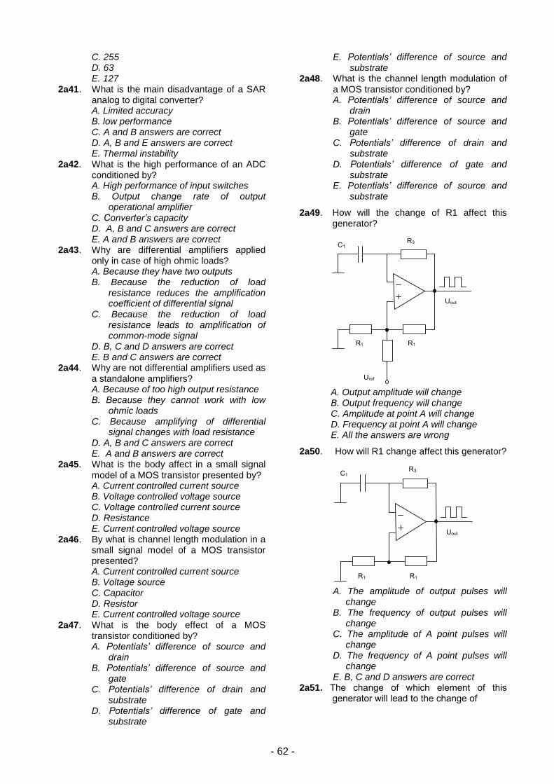
- 62 -
C. 255 D. 63 E. 127
2a41. What is the main disadvantage of a SAR analog to digital converter? A. Limited accuracy B. low performance C. A and B answers are correct D. A, B and E answers are correct E. Thermal instability
2a42. What is the high performance of an ADC conditioned by? A. High performance of input switches B. Output change rate of output
operational amplifier C. Converter’s capacity D. A, B and C answers are correct E. A and B answers are correct
2a43. Why are differential amplifiers applied only in case of high ohmic loads? A. Because they have two outputs B. Because the reduction of load
resistance reduces the amplification coefficient of differential signal
C. Because the reduction of load resistance leads to amplification of common-mode signal
D. B, C and D answers are correct E. B and C answers are correct
2a44. Why are not differential amplifiers used as a standalone amplifiers? A. Because of too high output resistance B. Because they cannot work with low
ohmic loads C. Because amplifying of differential
signal changes with load resistance D. A, B and C answers are correct E. A and B answers are correct
2a45. What is the body affect in a small signal model of a MOS transistor presented by? A. Current controlled current source B. Voltage controlled voltage source C. Voltage controlled current source D. Resistance E. Current controlled voltage source
2a46. By what is channel length modulation in a small signal model of a MOS transistor presented? A. Current controlled current source B. Voltage source C. Capacitor D. Resistor E. Current controlled voltage source
2a47. What is the body effect of a MOS transistor conditioned by? A. Potentials’ difference of source and
drain B. Potentials’ difference of source and
gate C. Potentials’ difference of drain and
substrate D. Potentials’ difference of gate and
substrate
E. Potentials’ difference of source and substrate
2a48. What is the channel length modulation of a MOS transistor conditioned by? A. Potentials’ difference of source and
drain B. Potentials’ difference of source and
gate C. Potentials’ difference of drain and
substrate D. Potentials’ difference of gate and
substrate E. Potentials’ difference of source and
substrate
2a49. How will the change of R1 affect this generator?
A. Output amplitude will change B. Output frequency will change C. Amplitude at point A will change D. Frequency at point A will change E. All the answers are wrong
2a50. How will R1 change affect this generator?
A. The amplitude of output pulses will
change B. The frequency of output pulses will
change C. The amplitude of A point pulses will
change D. The frequency of A point pulses will
change E. B, C and D answers are correct
2a51. The change of which element of this generator will lead to the change of
R1 R1
R3 C1
Uref
Uout
R1 R1
R3 C1
Uout
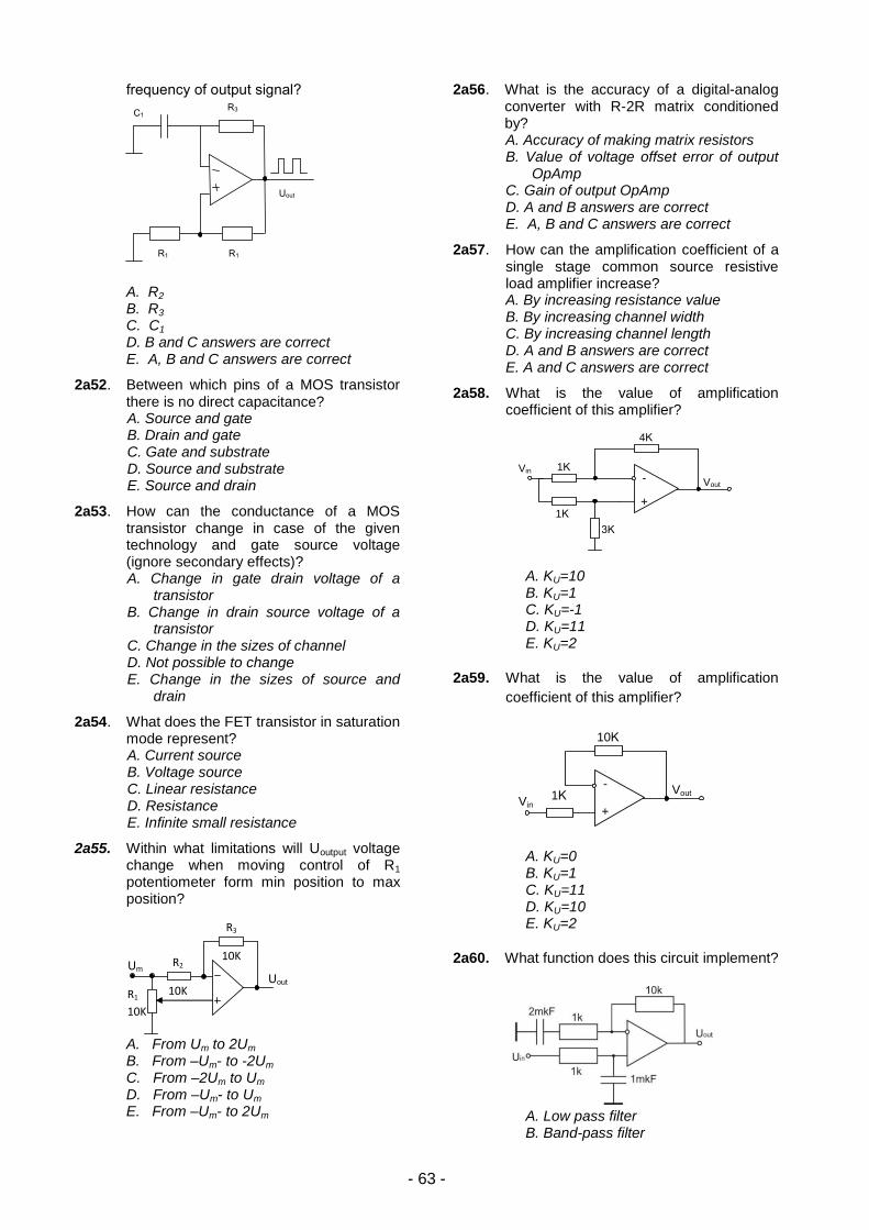
- 63 -
frequency of output signal?
A. R2 B. R3 C. C1 D. B and C answers are correct E. A, B and C answers are correct
2a52. Between which pins of a MOS transistor there is no direct capacitance? A. Source and gate B. Drain and gate C. Gate and substrate D. Source and substrate E. Source and drain
2a53. How can the conductance of a MOS transistor change in case of the given technology and gate source voltage (ignore secondary effects)? A. Change in gate drain voltage of a
transistor B. Change in drain source voltage of a
transistor C. Change in the sizes of channel D. Not possible to change E. Change in the sizes of source and
drain
2a54. What does the FET transistor in saturation mode represent? A. Current source B. Voltage source C. Linear resistance D. Resistance E. Infinite small resistance
2a55. Within what limitations will Uoutput voltage change when moving control of R1
potentiometer form min position to max position?
A. From Um to 2Um B. From –Um- to -2Um C. From –2Um to Um D. From –Um- to Um E. From –Um- to 2Um
2a56. What is the accuracy of a digital-analog converter with R-2R matrix conditioned by? A. Accuracy of making matrix resistors B. Value of voltage offset error of output
OpAmp C. Gain of output OpAmp D. A and B answers are correct E. A, B and C answers are correct
2a57. How can the amplification coefficient of a single stage common source resistive load amplifier increase? A. By increasing resistance value B. By increasing channel width C. By increasing channel length D. A and B answers are correct E. A and C answers are correct
2a58. What is the value of amplification coefficient of this amplifier?
A. KU=10 B. KU=1 C. KU=-1 D. KU=11 E. KU=2
2a59. What is the value of amplification
coefficient of this amplifier?
A. KU=0 B. KU=1 C. KU=11 D. KU=10 E. KU=2
2a60. What function does this circuit implement?
A. Low pass filter B. Band-pass filter
R1 R1
R3 C1
Uout
Um Uout
R1
10K
R2
10K
R3
10K
1K Vin
Vout
1K
4K
-
+
3K
Vin Vout 1K
10K
-
+
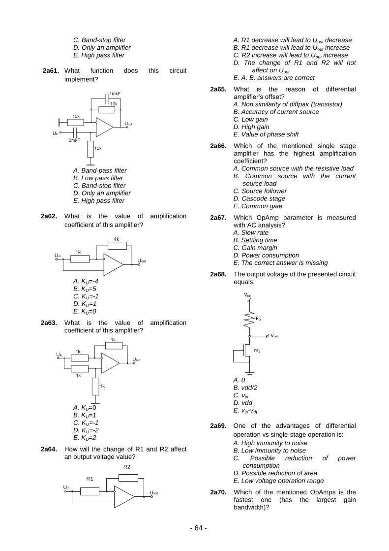
- 64 -
C. Band-stop filter D. Only an amplifier E. High pass filter
2a61. What function does this circuit
implement?
A. Band-pass filter B. Low pass filter C. Band-stop filter D. Only an amplifier E. High pass filter
2a62. What is the value of amplification
coefficient of this amplifier?
A. KU=-4 B. KU=5 C. KU=-1 D. KU=1 E. KU=0
2a63. What is the value of amplification coefficient of this amplifier?
A. KU=0 B. KU=1 C. KU=-1 D. KU=-2 E. KU=2
2a64. How will the change of R1 and R2 affect an output voltage value?
Uin
Uout
R2
R1
A. R1 decrease will lead to Uout decrease B. R1 decrease will lead to Uout increase C. R2 increase will lead to Uout increase D. The change of R1 and R2 will not
affect on Uout E. A. B. answers are correct
2a65. What is the reason of differential amplifier’s offset? A. Non similarity of diffpair (transistor) B. Accuracy of current source C. Low gain D. High gain E. Value of phase shift
2a66. Which of the mentioned single stage amplifier has the highest amplification coefficient? A. Common source with the resistive load B. Common source with the current
source load C. Source follower D. Cascode stage E. Common gate
2a67. Which OpAmp parameter is measured with AC analysis? A. Slew rate B. Settling time C. Gain margin D. Power consumption E. The correct answer is missing
2a68. The output voltage of the presented circuit equals:
A. 0 B. vdd/2 C. vin D. vdd E. vin-vth
2a69. One of the advantages of differential
operation vs single-stage operation is:
A. High immunity to noise B. Low immunity to noise C. Possible reduction of power
consumption D. Possible reduction of area E. Low voltage operation range
2a70. Which of the mentioned OpAmps is the fastest one (has the largest gain bandwidth)?
VDD
RD
Vout
m1
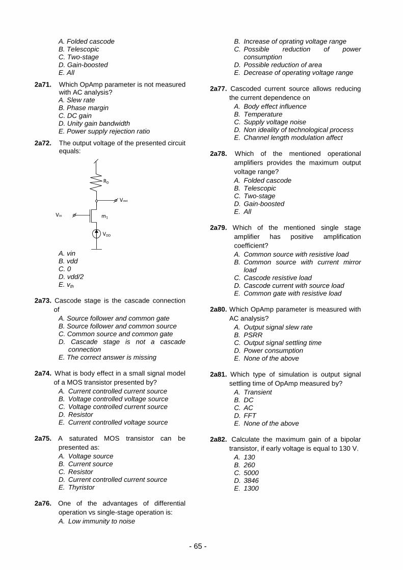
- 65 -
A. Folded cascode B. Telescopic C. Two-stage D. Gain-boosted E. All
2a71. Which OpAmp parameter is not measured with AC analysis? A. Slew rate B. Phase margin C. DC gain D. Unity gain bandwidth E. Power supply rejection ratio
2a72. The output voltage of the presented circuit equals:
A. vin B. vdd C. 0 D. vdd/2 E. vth
2a73. Cascode stage is the cascade connection
of
A. Source follower and common gate B. Source follower and common source C. Common source and common gate D. Cascade stage is not a cascade
connection E. The correct answer is missing
2a74. What is body effect in a small signal model
of a MOS transistor presented by? A. Current controlled current source B. Voltage controlled voltage source C. Voltage controlled current source D. Resistor E. Current controlled voltage source
2a75. A saturated MOS transistor can be
presented as:
A. Voltage source B. Current source C. Resistor D. Current controlled current source E. Thyristor
2a76. One of the advantages of differential
operation vs single-stage operation is: A. Low immunity to noise
B. Increase of oprating voltage range C. Possible reduction of power
consumption D. Possible reduction of area E. Decrease of operating voltage range
2a77. Cascoded current source allows reducing
the current dependence on A. Body effect influence B. Temperature C. Supply voltage noise D. Non ideality of technological process E. Channel length modulation affect
2a78. Which of the mentioned operational
amplifiers provides the maximum output
voltage range? A. Folded cascode B. Telescopic C. Two-stage D. Gain-boosted E. All
2a79. Which of the mentioned single stage
amplifier has positive amplification
coefficient?
A. Common source with resistive load B. Common source with current mirror
load C. Cascode resistive load D. Cascode current with source load E. Common gate with resistive load
2a80. Which OpAmp parameter is measured with
AC analysis? A. Output signal slew rate B. PSRR C. Output signal settling time D. Power consumption E. None of the above
2a81. Which type of simulation is output signal
settling time of OpAmp measured by? A. Transient B. DC C. AC D. FFT E. None of the above
2a82. Calculate the maximum gain of a bipolar
transistor, if early voltage is equal to 130 V. A. 130 B. 260 C. 5000 D. 3846 E. 1300
RD
Vout
m1 Vin
VDD
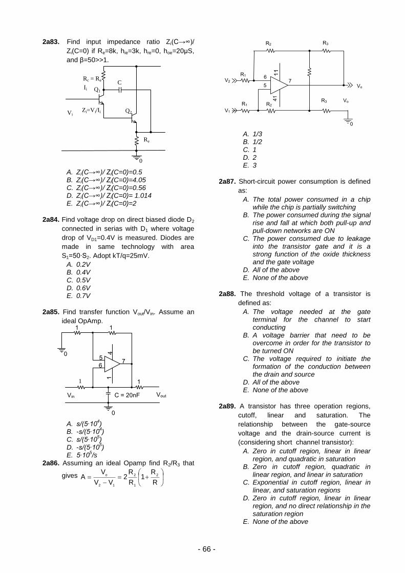
- 66 -
2a83. Find input impedance ratio Zi(C→∞)/
Zi(C=0) if Re=8k, hie=3k, hre=0, hoe=20μS,
and β=50>>1.
A. Zi(C→∞)/ Zi(C=0)=0.5 B. Zi(C→∞)/ Zi(C=0)=4.05 C. Zi(C→∞)/ Zi(C=0)=0.56 D. Zi(C→∞)/ Zi(C=0)= 1.014 E. Zi(C→∞)/ Zi(C=0)=2
2a84. Find voltage drop on direct biased diode D2
connected in serias with D1 where voltage
drop of VD1=0.4V is measured. Diodes are
made in same technology with area
S1=50∙S2. Adopt kT/q=25mV. A. 0.2V B. 0.4V C. 0.5V D. 0.6V E. 0.7V
2a85. Find transfer function Vout/Vin. Assume an
ideal OpAmp.
A. s/(5∙10
4)
B. -s/(5∙104)
C. s/(5∙105)
D. -s/(5∙105)
E. 5∙105/s
2a86. Assuming an ideal Opamp find R2/R3 that
gives
R
R1
R
R2
VV
VA 2
1
2
12
o
A. 1/3 B. 1/2 C. 1 D. 2 E. 3
2a87. Short-circuit power consumption is defined
as: A. The total power consumed in a chip
while the chip is partially switching B. The power consumed during the signal
rise and fall at which both pull-up and pull-down networks are ON
C. The power consumed due to leakage into the transistor gate and it is a strong function of the oxide thickness and the gate voltage
D. All of the above E. None of the above
2a88. The threshold voltage of a transistor is
defined as: A. The voltage needed at the gate
terminal for the channel to start conducting
B. A voltage barrier that need to be overcome in order for the transistor to be turned ON
C. The voltage required to initiate the formation of the conduction between the drain and source
D. All of the above E. None of the above
2a89. A transistor has three operation regions,
cutoff, linear and saturation. The
relationship between the gate-source
voltage and the drain-source current is
(considering short channel transistor): A. Zero in cutoff region, linear in linear
region, and quadratic in saturation B. Zero in cutoff region, quadratic in
linear region, and linear in saturation C. Exponential in cutoff region, linear in
linear, and saturation regions D. Zero in cutoff region, linear in linear
region, and no direct relationship in the saturation region
E. None of the above
Vo
R3 R2
R1
7
11
6
5
V1
R1
41
R2 Vo
V2
R3
0
1
k
1 1
1k
7
1k
1k
0 5
6
4
C = 20nF Vin Vout
0
Zi=Vi/Ii
Ii
Vi
C Q1
Q2
Re
Rc = Re
0
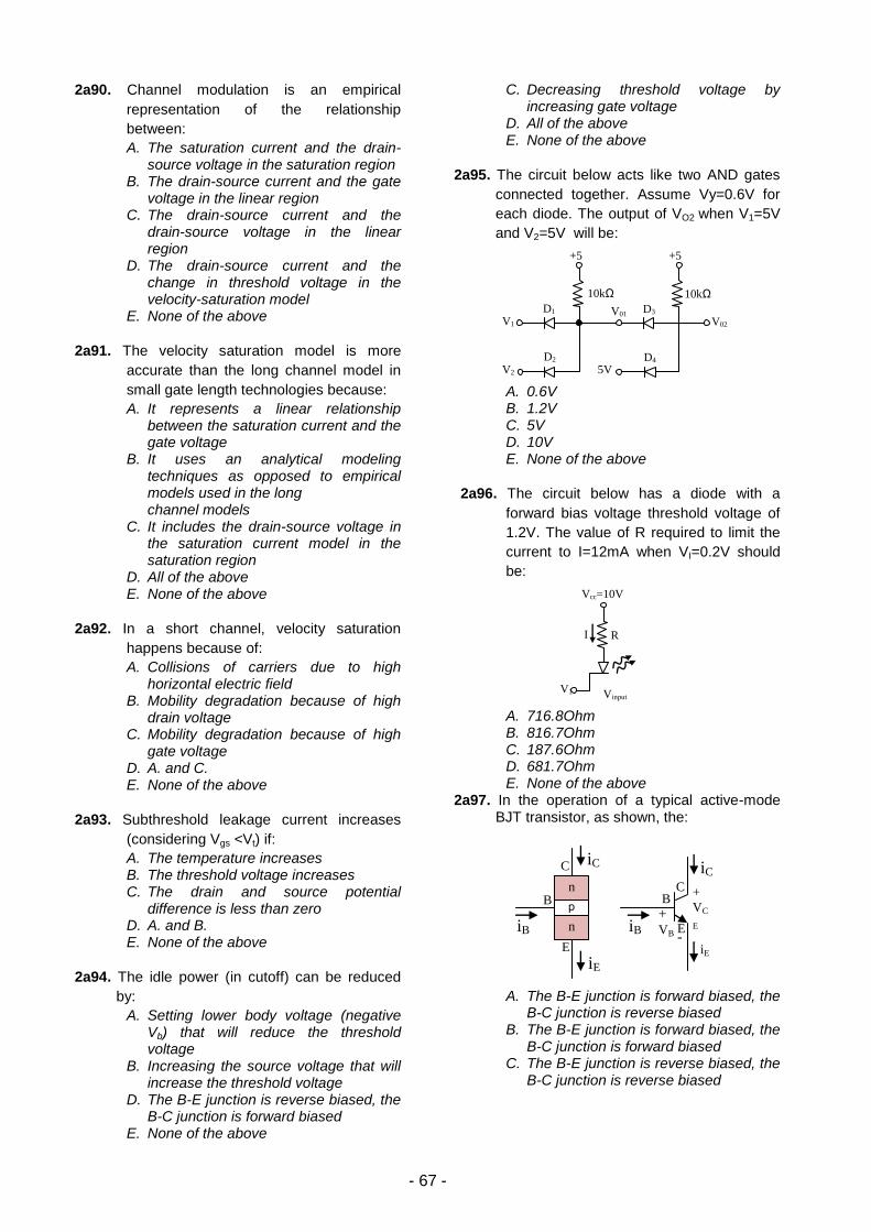
- 67 -
2a90. Channel modulation is an empirical
representation of the relationship
between: A. The saturation current and the drain-
source voltage in the saturation region B. The drain-source current and the gate
voltage in the linear region C. The drain-source current and the
drain-source voltage in the linear region
D. The drain-source current and the change in threshold voltage in the velocity-saturation model
E. None of the above
2a91. The velocity saturation model is more
accurate than the long channel model in
small gate length technologies because: A. It represents a linear relationship
between the saturation current and the gate voltage
B. It uses an analytical modeling techniques as opposed to empirical models used in the long channel models
C. It includes the drain-source voltage in the saturation current model in the saturation region
D. All of the above E. None of the above
2a92. In a short channel, velocity saturation
happens because of: A. Collisions of carriers due to high
horizontal electric field B. Mobility degradation because of high
drain voltage C. Mobility degradation because of high
gate voltage D. A. and C. E. None of the above
2a93. Subthreshold leakage current increases
(considering Vgs <Vt) if:
A. The temperature increases B. The threshold voltage increases C. The drain and source potential
difference is less than zero D. A. and B. E. None of the above
2a94. The idle power (in cutoff) can be reduced
by: A. Setting lower body voltage (negative
Vb) that will reduce the threshold voltage
B. Increasing the source voltage that will increase the threshold voltage
C. Decreasing threshold voltage by increasing gate voltage
D. All of the above E. None of the above
2a95. The circuit below acts like two AND gates
connected together. Assume Vy=0.6V for
each diode. The output of VO2 when V1=5V
and V2=5V will be:
A. 0.6V B. 1.2V C. 5V D. 10V E. None of the above
2a96. The circuit below has a diode with a
forward bias voltage threshold voltage of
1.2V. The value of R required to limit the
current to I=12mA when VI=0.2V should
be:
A. 716.8Ohm B. 816.7Ohm C. 187.6Ohm D. 681.7Ohm E. None of the above
2a97. In the operation of a typical active-mode BJT transistor, as shown, the:
A. The B-E junction is forward biased, the
B-C junction is reverse biased B. The B-E junction is forward biased, the
B-C junction is forward biased C. The B-E junction is reverse biased, the
B-C junction is reverse biased
D. The B-E junction is reverse biased, the B-C junction is forward biased
E. None of the above
p
iC
iE
iB
B
E
C
C
iC
+
VC
E
-
B
E
iE
iB + VB
E
-
n
n
Vcc=10V
R I
V1 Vinput
+5V
+5V
V1
V2 5V
10kΩ 10kΩ
V01 V02
D1
D2
D3
D4
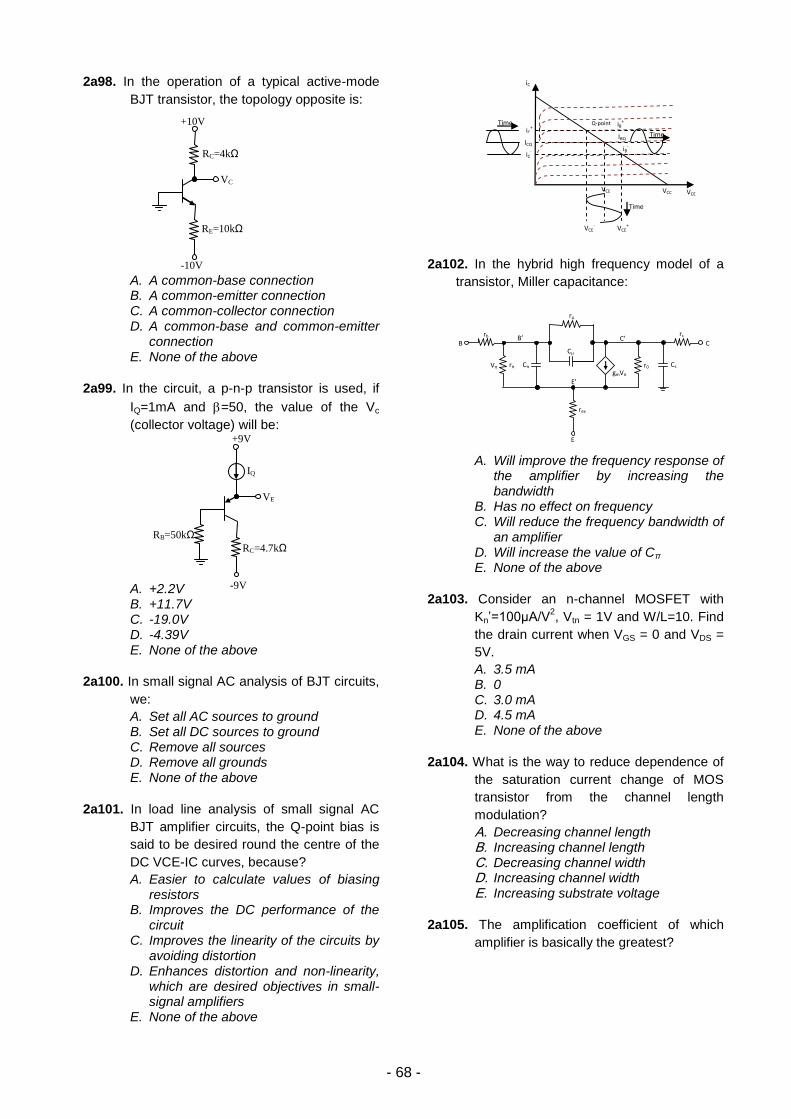
- 68 -
2a98. In the operation of a typical active-mode
BJT transistor, the topology opposite is:
A. A common-base connection B. A common-emitter connection C. A common-collector connection D. A common-base and common-emitter
connection E. None of the above
2a99. In the circuit, a p-n-p transistor is used, if
IQ=1mA and =50, the value of the Vc
(collector voltage) will be:
A. +2.2V B. +11.7V C. -19.0V D. -4.39V E. None of the above
2a100. In small signal AC analysis of BJT circuits,
we: A. Set all AC sources to ground B. Set all DC sources to ground C. Remove all sources D. Remove all grounds E. None of the above
2a101. In load line analysis of small signal AC
BJT amplifier circuits, the Q-point bias is
said to be desired round the centre of the
DC VCE-IC curves, because? A. Easier to calculate values of biasing
resistors B. Improves the DC performance of the
circuit C. Improves the linearity of the circuits by
avoiding distortion D. Enhances distortion and non-linearity,
which are desired objectives in small-signal amplifiers
E. None of the above
2a102. In the hybrid high frequency model of a
transistor, Miller capacitance:
A. Will improve the frequency response of
the amplifier by increasing the bandwidth
B. Has no effect on frequency C. Will reduce the frequency bandwidth of
an amplifier D. Will increase the value of Cπ E. None of the above
2a103. Consider an n-channel MOSFET with
Kn’=100μA/V2, Vtn = 1V and W/L=10. Find
the drain current when VGS = 0 and VDS =
5V. A. 3.5 mA B. 0 C. 3.0 mA D. 4.5 mA E. None of the above
2a104. What is the way to reduce dependence of
the saturation current change of MOS
transistor from the channel length
modulation?
A. Decreasing channel length B. Increasing channel length C. Decreasing channel width D. Increasing channel width E. Increasing substrate voltage
2a105. The amplification coefficient of which
amplifier is basically the greatest?
Time
iB+
IBQ ICQ
Time iC
+
iC-
iB-
VCC VCE
Time
VCE- VCE
+
VCE
Q
Q-point
iC
B B’ C’
Cs
rc
r0
rex
E
E’
gmVπ rπ Cπ Vπ
C Cμ
rμ
rb
RC=4kΩ
RE=10kΩ
+10V
-10V
VC
RC=4.7kΩ
RB=50kΩ
+9V
-9V
VE
IQ

A. Common source with current source load
B. Source follower with resistive load C. Common gate with current source load D. Common source with resistive load E. Common gate with resistive load
2a106. What type of load ensures greatest
amplification coefficient of a MOS
transistor based amplifier?
A. Resistive B. Diode connected C. Triode mode D. Current source E. Cutoff mode
2a107. The operating domain of output voltage of
which amplifier is basically the greatest?
A. Common source with current source load
B. Cascode with resistive load C. Common gate with current source load D. Common source with resistive load E. Common gate with resistive load
2a108. How does the output common mode
voltage of a differential amplifier depend
on the input common mode voltage?
A. Direct B. Inverse C. Does not depend D. (Vout/Vin)cm=gmRD E. Equal
2a109. How will the output common mode voltage
of a differential amplifier with n-MOS input
change if tail current increases (Iss)?
A. Will decrease B. Will increase C. Will not change D. The output common mode voltage of a
differential amplifier does not depend on tail current (Iss)
E. Will increase 3 times
2a110. Which parameter of an OpAmp is
measured with AC analysis?
A. Slew rate B. Power supply rejection ratio C. Settling time D. Power consumption E. Offset error
2a111. Which parameter of an OpAmp is
measured with transient analysis?
A. Gain bandwidth B. Power supply rejection ratio C. Settling time D. Unity gain bandwidth E. Phase margin
2a112. With which analysis does the gain
bandwidth of an OpAmp measured?
A. Transient B. DC C. AC D. FFT E. The correct answer is missing
2a113. Which OpAmp-based circuit has
hysteresis transfer characteristics?
A. Positive feedback comparator B. Integrator C. Comparator without feedback D. Non-inverting amplifier E. Inverting amplifier
2a114. What else is an active integrator?
A. High pass filter B. Low pass filter C. Differentiator D. Bandpass filter E. Nothing
2a115. What else is a differentiator?
A. High pass filter B. Low pass filter C. Integrator D. Bandpass filter E. Nothing
2a116. Which ADC is basically the fastest?
A. Pipeline B. Sigma-delta C. Integrating D. Flash E. SAR
2a117. Which ADC has basically the highest bit?
A. Pipeline B. Sigma-delta C. Integrating D. Flash E. SAR
2a118. In what ADC structure there is DAC?
A. Dual integrating B. Sigma-delta C. Integrating D. Flash E. SAR
2a119. Which DAC is basically the fastest?
A. R-string B. R-2R C. Pipeline D. Current steering E. Charge scaling
2a120. For the OpAmp circuit shown below, what
is the value of V0 when Vi = 0V? The
OpAmp and diodes are ideal.
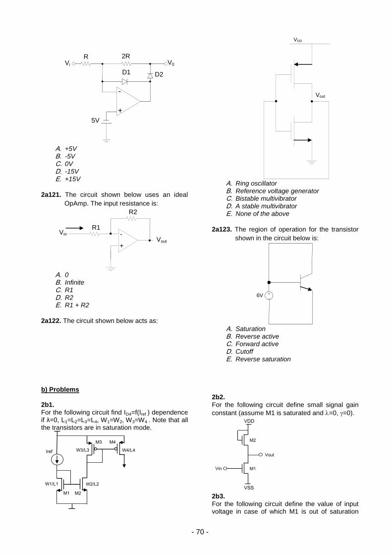
- 70 -
A. +5V B. -5V C. 0V D. -15V E. +15V
2a121. The circuit shown below uses an ideal
OpAmp. The input resistance is:
A. 0 B. Infinite C. R1 D. R2 E. R1 + R2
2a122. The circuit shown below acts as:
A. Ring oscillator B. Reference voltage generator C. Bistable multivibrator D. A stable multivibrator E. None of the above
2a123. The region of operation for the transistor
shown in the circuit below is:
A. Saturation B. Reverse active C. Forward active D. Cutoff E. Reverse saturation
b) Problems 2b1. For the following circuit find ID4=f(Iref ) dependence if λ=0, L1=L2=L3=L4, W1=W2, W3=W4 . Note that all the transistors are in saturation mode.
2b2. For the following circuit define small signal gain
constant (assume M1 is saturated and =0, =0).
2b3. For the following circuit define the value of input voltage in case of which M1 is out of saturation
M1 M2
M3 M4
W3/L3
W1/L1 W2/L2
W4/L4 Iref
VDD
VSS
M1
M2
Vin
Vout
6V + -
VDD
Vout
-
+
Vin Vout
R1
R2
-
+
Vi
R 2R
D1 D2
V0
5V
- 71 -
mode if (W/L)1=49 (W/L)2=9 VTH=0.7 VDD=3,
=0.
2b4. A current mirror is given by transistors’ geometrical sizes. Find the gate voltage of M1 transistor.
2b5. For the following circuit find the drain current of M4 transistor if all the transistors are in saturation. Ignore channel length modulation (λ=0).
2b6.
For the following circuit find Vref, if n=550 cm2/Vs,
εSi02=3.9, ε0=8.85*10-14
F/cm,
tox=0.16 nm, Vthn=0.8V, VDD=2V, VSS=0V, W=L=10 um, λ=0, R=10 kOhm.
2b7. For the following circuit define how much Iout will
change if VDD changes by 10% and if the transistor is in saturation and W=50um, L=0.5um,
Iout=0.5mA, Kn=120 uA/V
2, VTH=0.5V VDD=3V,
(nominal value), R2/R1=0.35, =0.
2b8. Find the cutoff frequency of the following circuit and build amplitude-frequency characteristics, if R1, R2 and C are known.
2b9. What does Iout equal to when the transistor is in saturation (express transistor’s conductivity by gm). Ignore body effect and channel modulation.
2b10. Find Vout depending on Vin, if the transistor is in saturation. Ignore body effect and channel modulation.
2b11. R1, R2, R3, R4 resistances are given. Find
3in2in1inout V,V,VfV , considering the real KA
amplifying coefficient.
VDD
VSS
M1
M2
Vin
Vout
W2/L2
W1/L1
M1
M2 M4
M3
100/5
100/5
100/5
100/5
I R
-2.5V
+2.5V
ID4
M1 M2
M3 M4
W3/L3
W1/L1 W2/L2
Iref W4/L4
VDD
R
Vref
VSS
VDD
R1
VSS
Iout
R2
A
-
+
R2 R1
C
m1
RD
RF Vb
VDD
Vout
Vin
Iout
m1
R1
R2
VG
VDD

- 72 -
2b12.
nL
W
, pL
W
, refI , 1R values are given. Find
outV ,
ignore channel modulation.
2b13. For the following circuit find the ID4=f(Iref) dependence, if λ=0, L1=L2=L3=L4, W1=W2=3W3=6W4 . All the transistors are saturated.
2b14. Calculate how much will Iout change if VDD
increases by 10%: Given W, L, n, VTH, COX, R2, R1. The transistor is saturated. Ignore secondary effects.
2b15. Calculate the value of R if M1 transistor is
saturated and VDD, Vref, VTH, , R1, R2, =0 are given. 2b16.
Find
coefficent (by variable
component). Given .
2b17.
Find Av=dVout/dVin small signal gain: gm1, gm2, gm3,
R1 values are known. Ignore secondary effects.
2b18.
Find Av=dVout/dVin small signal gain: gm1,gmb1, R1,
R2 values are known. Ignore channel length
modulation.
m1
Vout
R1 nL
W
5nL
W
m2
pL
W
5pL
W
m3 m4 refI
ID4
M1 M2
M3 M4
W3/L3
W1/L1 W2/L2
Iref W4/L4
VDD
R1
VSS
Iout
R2
A
VDD
R1
VSS
I2
R2
I1
I
Vref
M3 M2
R1 M1 Vin
Vout
VDD
M3 M2
R1 M1 Vin
Vout
VDD
VDD
R1
Vout
Vin
R2
Vb
R1 Vin1
Vout
Vin2
Vin3
R2
R3
R4
-
+
- 73 -
2b19. Sketch Vout versus Vin as Vin varies from 0 to VDD. Identify the important transition points.
2b20. Calculate the maximum gain and central frequency of the filter based on OpAmp if R1=1kOhm, R2=2 kOhm, R3=10 kOhm,C1=10mkF, C1=1mkF.
Uin
R1
R2
R3
C2
C1
2b21. The sequence ( ) cos( / 4)x n n is a result of
0( ) cos 2u t f t analog signal sampling with
sampling frequency fs=1000 Hz: ( ) ( )x n u n t
where Δt=1/fs. Find two minimum f0 values for which it takes place. 2b22.
The sequence ( ) cos( / 4)x n n is a result of
0( ) cos 2u t f t
analog signal sampling with
sampling frequency fs=800 Hz: ( ) ( )x n u n t ,
where Δt=1/fs. Find two minimum f0>200 Hz values for which it takes place. 2b23. Find Av=dVout/dVin small signal gain. gm1, gm2, gm3, r01, r02, r03, R1 values are known.
2b24.
Find Av=dVout/dVin small signal gain. gm1, gmb1, R1, R2 values are known. Ignore channel length modulation.
2b25.
Sketch Vout versus Vin, as Vin varies from 0 to VDD. Identify the important transition points. Find Av=dVout/dVin small signal gain. gm1, gm2, R1, R2 values are known. Ignore channel length modulation. R1<R2 .
2b26.
Sketch Vout versus Vin, as Vin varies from 0 to VDD. Identify the important transition points. Find Av=dVout/dVin small signal gain. gm1, gm2, RD values are known. Ignore channel length modulation.
VDD
R1
Vout
Vin
R2
Vb
VSS
Vin
m1
VDD
Vb
Vout
R2
R1
m1 Vin
R2 Vout
m2
R1
VDD
Vx
M1 Vin
R1
Vout
M3 M2
VDD
- 74 -
2b27.
The following circuit should be analyzed with an AC analysis for a sine shaped input current signal. The circled numbers represent the node labels.
Give the value for all elements in the matrix, Yxy and Ax4, and right side vector Inx for a modified nodal analysis in the frequency domain.
4
3
2
1
1
3
2
1
44434241
34333231
24232221
14131211
n
n
n
n
n
n
n
I
I
I
I
i
u
u
u
AYYY
AYYY
AYYY
AYYY
2b28.
An NMOS transistor has a threshold voltage of 0.4V and a supply voltage of VDD=1.2V. The threshold voltage (Vt) has to be reduced by 100mV to obtain faster device. Consider the constants in Table 1, unless otherwise specified in the question.
a) By what factor would the saturation current increase (at Vgs=Vds=Vdd)? Consider velocity saturation model.
b) By what factor would the sub-threshold leakage current increase at room temperature (25C, 300K) at Vgs =0 and Vds=Vdd? Assume n = 1.4, and Voffset= 0.
c) By what factor would the sub-threshold leakage current change at T= 400K? Will it increase or decrease? Assume the threshold voltage is independent of T.
d) Assume the threshold voltage has to be reduced by increasing the body voltage (using body effect), what would be the value of Vsb to reach the targeted Vt?
2b29.
For the 90nm technology, the device parameters are about the same as for 130 nm technology except for Vt0 (zero-bias threshold voltage) and tox (oxide capacitance per unit area). The channel length is L=80nm (due to lateral diffusion). In order to determine Vt0 and tox, some device measurements are made on an NMOS transistor with W = 400nm to produce the results shown in the table below. Estimate the value of Vt0 and tox from these measurements (ECL term can be ignored). Consider the constants in Table 1, unless otherwise specified in the question.
Vds (V) Vgs (V) Vsb (V) Ids (µA)
1.2 1.2 0.0 78.70
1.2 1.2 0.5 85.28
1.2 1.0 0.0 56.21
1.2 0.8 0.0 33.72
1.2 0.6 0.0 11.24
2b30.
Consider an NMOS transistor. Assume that the transistor has W=900nm, L=180nm and source/gate and drain/gate overlap of 20nm. Let tox =40 Å (Angstroms). Compute the worst-case gate capacitance per unit width, Cg, in units of fF/um. Estimate Cgs, Cgd and Cgb in linear, saturation and cutoff, including overlap effects. Consider the constants in Table 1, unless otherwise specified in the question.
Table 1. Data used 2b28-2b30 problems
Iosin(⍵t) u1 G1 C1
1
2
i1=ku1 G2
3
0
VDD=1.2V |VTP|=VTN = 0.4V Ecn = 6V/m Ecp = 24 V/m
vsat = 8*106 cm/sec 2|F| = 0.88V en =270 cm2/V-sec ep =70 cm2/V-sec
= 0.2(V1/2
) λ=0.01V-1
q =1.6*10-19
C n =1.4
T = 300 oK (27
oC) k = 1.38*10
-23 J/
oK o = 8.85*10
-14 F/cm ox = 3.970
L= 100nm xd =20nm Reqn = 12.5 kΩ/☐ Reqp = 30.0 kΩ/☐
Cox = 1.6x10⁻⁶
F/cm2 Cg = 2 fF/um Ceff = 1fF/um Cu = 1.7-cm
Wint = 0.17m Tint = 0.8m Cint = 0.2fF/m Voffset = 0
Vin m1
Vout
RD
m2
VDD
- 75 -
2b31. Show the dependence of Ix from Vx, when Vx changes from 0 to VDD. gm1,VTH1, R1, R2 values are known. Ignore secondary effects.
2b32. Find Av=dVout/dVin small signal amplification coefficient. gm1, gm2, RS, VTH1, VTH2, r01, r02 values are known. Ignore body effect. M1 and M2 are saturated.
2b33. Get the output signal expression of inverse amplifier, built by OpAmp, considering OpAmp’s K’u real amplification coefficient and input resistance for R’in differential signal (take Uin>0). Compare it with the version of an ideal OpAmp.
2b34. Get the amplification coefficient expression of non-inverse amplifier, built by OpAmp, considering OpAmp’s K`u real amplification coefficient and input resistance for R`in differential signal (take Uin>0). Compare it with the version of an ideal OpAmp.
Uout R
1
R
2
I1
+
I2
Ui
n
Uout Uin
R
1
R
2
I1
+
I2
VDD
M1
Vout
Vin
M2
RS
Vb2
Vb1
+
-
VDD
M1
IX
VX
R1
R2
1
IDm2
U-
U-
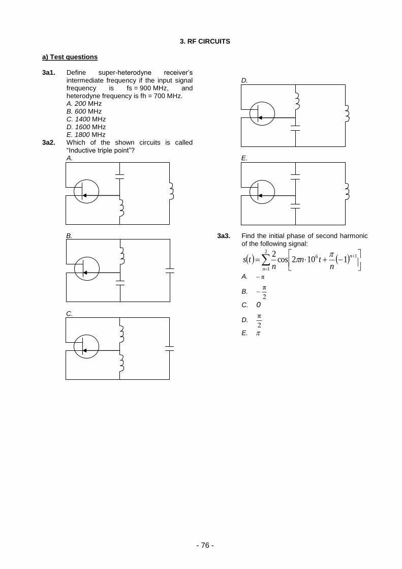
- 76 -
3. RF CIRCUITS
a) Test questions 3a1. Define super-heterodyne receiver’s
intermediate frequency if the input signal frequency is fs = 900 MHz, and heterodyne frequency is fh = 700 MHz. A. 200 MHz B. 600 MHz C. 1400 MHz D. 1600 MHz E. 1800 MHz
3a2. Which of the shown circuits is called “Inductive triple point”? A.
B.
C.
D.
E. 3a3. Find the initial phase of second harmonic
of the following signal:
2
1
16 1102cos2
n
n
ntn
nts
A. π
B. 2
π
C. 0
D. 2
π
E.
- 77 -
4. SEMICONDUCTOR PHYSICS AND ELECTRONIC DEVICES
a) Test questions 4a1. Which circuit based on operational
amplifier has transfer function with hysteresis? A. Non-inverting amplifier B. Inverting adder C. Comparator without feedback D. Comparator with positive feedback E. Comparator with negative feedback
4a2. Does semiconductor diode's I/V characteristics differ from I/V characteristics of ohmic resistance? A. Yes, it depends on the applied
voltage direction and is nonlinear B. Yes, it depends on the applied
voltage direction and is linear C. No, as the more direct voltage, the
more is the current D. Partially, as current exists irrespective
of voltage direction E. The correct answer is missing
4a3. What parameters of semiconductor
material are needed for transistor fabrication? A. Charge carriers' mobility and
concentration B. Charge carriers' concentration,
minority charge carriers' life time, mobility
C. Charge carriers' concentration and diffusion coefficient
D. Charge carriers' concentration, diffusion coefficient, mobility, band gap
E. The correct answer is missing 4a4. Which regions does the graph of drain
current dependence on source-drain voltage for p-n junction field effect transistor consist of? A. Linear dependence, saturation B. Linear dependence, saturation,
breakdown C. Linear dependence, transition,
saturation, breakdown D. Linear dependence, transition,
breakdown E. The correct answer is missing.
4a5. How are the oxide layer capacitor C0, the
surface state capacitor Css and the differential capacitor of the surface charge layer connected between one another in a MOS structure? A. Css and C0 parallel, and with Csc
sequentially B. Css and Csc parallel, and with C0
sequentially
C. C0 and Csc sequentially, and with Csc parallel
D. All capacitors are connected parallel to one another
E. The correct answer is missing.
4a6. How does differential resistance of p-n junction change parallel to direct current increase? A. Does not change B. Decreases C. Increases D. Increases, then decreases E. The correct answer is missing
4a7. How many times will diffusion capacitance of a bipolar transistor increase if its base length increases twice? A. Will not change
B. Will increase 2 times
C. Will increase 4 times D. Will decrease twice E. The correct answer is missing
4a8. How does the p-n-p bipolar transistor's transfer factor depend on diffusion length
of holes pL ?
A. No dependence
B. Increase with the increase of pL by
pL2
W1β law
C. Increase with the increase of pL by
2
pL
W
2
11
β law
D. Decreases E. The correct answer is missing
4a9. The light of what maximum wavelength
can affect the current of silicon ( 1.1gE
eV) photodiode?
A. 1130max nm
B. 550max nm
C. 1240max nm
D. 335max nm
E. The correct answer is missing 4a10. How is bipolar transistor's current gain
expressed in common base circuit with
the help of emitter effectiveness ,
transition coefficient and collector's avalanche multiplication factor M ?
A. M

- 78 -
B. M
C. M
D. M
E. The correct answer is missing 4a11. Is operating temperature range of ICs,
computers and other semiconductor devices conditioned by the used semiconductor material's band gap? A. Yes, the more the band gap, the more
temperature range B. No, as concentration of minority
charge carriers is independent from temperature
C. Conditioned partially as by increasing the temperature, carriers' mobility decreases
D. No, as band gap does not depend on temperature
E. The correct answer is missing 4a12. Which expression is wrong?
A. Diode subtypes are: point-junction diodes, stabilitrons, varicaps and tunnel diodes
B. In tunnel diodes reverse current for the same voltage is higher than direct current value
C. In varicaps with increase of voltage barrier capacitance increases
D. Schottky diodes operation is based on processes which take place in semiconductor-metal contact
E. The response time of Schottky diodes, therefore, frequency properties are conditioned by barrier capacitance
4a13. Field effect transistors, compared with
bipolar transistors A. Have small input resistance B. Have small noise coefficient C. The current is at the same time
conditioned by electrons and holes D. Provide current amplification E. The performance is mainly
conditioned by injection of minority carriers
4a14. Through which device is the electrical
signal amplification implemented? A. Resistor B. Capacitor and inductor C. Diode D. Transistor E. Photodiode
4a15. How many pins does the field effect transistor have? A. 1 gate
B. 2 sources and 1 drain C. 3 sources, 1 gates and 1 drain D. 2 bases and 1 collector E. 1 source, 1 gate and 1 drain
4a16. Is the gate of a field effect transistor
isolated from its channel? A. Yes B. No C. Partially and there is weak tunnel
coupling D. In saturation mode of field effect
transistor most part of channel current flows through gate
E. The correct answer is missing 4a17. n – type Ge sample, which is anticipated
for making a transistor, has 1.5 Ohmcm specific resistance and 5.410
3 cm
3/Kl
Holy coefficient. What does the charge carriers' concentration and their mobility equal? A. 1.610
21 m-3, 5 m
2/Vs
B. 1.61021
m-3, 0.1 m2/Vs
C. 1.161021
m-3, 0.36 m2/Vs
D. 21020
m-3, 0.36 m2/Vs
E. The correct answer is missing. 4a18. By means of what semiconductor device
can light influence be detected? A. Posistor B. Resistor C. Photodiode D. Capacitor E. Inductor
4a19. Which materials' conductivity is higher?
A. Dielectrics B. Semiconductors C. Metals D. All have low conductivity E. All have high conductivity
4a20. How does the negative differential
resistance current range change depending on the density of lightly degenerated n-region impurities in tunnel diode? A. Interval decreases when increasing
density B. Interval increases when increasing
density C. It is not conditioned by density of
impurity D. Interval increases when reducing
density E. All the conditions are true
4a21. Generally, what is the response time of
photodiode conditioned by? A. The diffusion time of equilibrium
carriers in the base

- 79 -
B. Their transit time through the layer of p-n junction
C. RC constant of diode structure D. Only A and C E. Conditions A, B, C
4a22. Which statement mentioned below is not true for ohmic contact? A. Electrical resistance of ohmic contact
is small B. Electrical resistance of ohmic contact
does not depend on the current direction if the current value does not exceed the given value
C. Electrical resistance of ohmic contact does not depend on the current direction in case of any current value flowing through it
D. Most part of ohmic contacts is formed on the basis of n-n+ or p-p+ type contacts
E. All the answers are correct
4a23. By increasing the lifetime of electrons 4 times, their diffusion length A. Increases 4 times B. Increases twice C. Does not increase D. Reduces twice E. The correct answer is missing
4a24. What does the generation frequency
depend on in Gunn diode? A. Mobility speed of field domain B. Impurity density in semiconductor C. Sample length D. Dielectric permeability of material E. All the answers are correct
4a25. How can the cutoff voltage of MOS
transistor change? A. By opposite voltage of substrate-
channel junction, when substrate is higher ohmic than the channel
B. By opposite voltage of substrate-channel junction when substrate resistance is equal or smaller than the channel resistance
C. By voltage applied to the gate D. By A and C E. By B and C
4a26. Which statement is wrong for unipolar
transistors? A. In unipolar transistors, physical
processes of current transport are conditioned by one sign carriers-electrons or holes
B. In unipolar transistors, physical processes of current transport are conditioned by the injection of minority carriers.
C. In unipolar transistors current control is carried out by the vertical electrical field
D. The surface channel unipolar transistor includes metal-dielectric-semiconductor structure
E. The correct answer is missing 4a27. What is the high frequency property of
Schottky diode conditioned by? A. Moving the majority carriers through
diode B. Excluding minority carriers’
accumulation in diode C. Value of Schottky barrier D. Impurity density in a semiconductor E. Only C and D
4a28. Which of the below written statements is
wrong for an integrated capacitor? A. An integrated capacitor represents IC
element consisting of conductive electrodes (plates), divided by isolation layer
B. In ICs the role of an integrated capacitor is often performed by reverse-biased p-n junctions of a transistor structure
C. The quality factor of an integrated capacitor is defined by the following:
CRfQ 2 where f
operating frequency, C
capacitance of a capacitor, Rresistance of a resistor sequentially connected with the transistor
D. The quality factor of an integrated capacitor characterizes loss of power at capacitive current junction
E. All the answers are correct 4a29. Which of the below mentioned statements
is wrong for electronic lithography? A. In this method the electron beams are
used as a source of radiation B. The method of electron beam
lithography is based on non-thermal influence left by electron beam on resist
C. The ultraviolet beams fall on resist surface at electron beam lithography
D. It is possible to reduce diffraction effects by increasing the electron accelerating voltage in electron beam lithography
E. The correct answer is missing 4a30. Which of the below mentioned statements
is correct for a bipolar transistor in saturation mode? A. Emitter and collector junctions are
forward-biased B. Emitter junction is forward-biased,
and collector junction –reverse-biased

- 80 -
C. Transistor base resistance in this mode is maximum, as emitter and collector junctions inject large number of free particles to base region
D. Free carriers’ extraction takes place from transistor base being in this mode
E. The correct answer is missing 4a31. What crystallographic plane is underlined
in cubic lattice?
A. (100) B. (101) C. (001) D. (011) E. (110)
4a32. Due to what properties is silicon considered the main material of microelectronics? A. Exclusive combination of its band gap
and electro-physical parameters B. Its oxide stability and isolating
properties C. High development of technological
methods related to it in different physical-chemical processes
D. The value of its natural resources E. All the answers are correct
4a33. What statement is wrong for metal-nitride-oxide semiconductor (NMOS) field effect transistor? A. In a such transistor, silicon nitride and
silicon dioxide double structure serves as a subgate isolator
B. There are many deep levels (traps) for electrons in silicon nitride layer
C. The layer’s thickness of silicon dioxide is selected such that it is not tunnel transparent
D. After removing the voltage on MNOS-field transistor’s gate, the injected charge remains long trapped which corresponds to the existence of induced inversion layer.
E. The correct answer is missing
4a34. If the density of semiconductor’s defects is large, A. The lifetime of carriers will be large B. The conductivity of semiconductor will
decrease
C. The recombination speed will increase
D. The current will remain constant E. The generation speed will increase
4a35. The performance of tunnel diodes is larger than the one of p – n junction as A. Injection level is large B. Injection mechanism is different C. Junction capacitance is small D. Current is formed by electrons and
holes E. Potential barrier’s height is small
4a36. What diode is called stabilitron? A. Direct current of which exponentially
increases with the voltage B. Reverse current of which is saturated C. Reverse branch of its the volt-ampere
characteristic has a region very strict dependence of current on voltage
D. The volt-ampere characteristic of which has an N- type region
E. The correct answer is missing 4a37. Threshold voltage of a short channel MOS
transistor is smaller than the one of a long channel MOS as A. It occupies smaller area B. The number of technological
processes is small C. Gate controls smaller number of
charge D. There are piled charges on the
boundary of oxide-semiconductor junction
E. Intrinsic capacitance is large
4a38. In Gann diode, negative conductivity occurs A. Due to ohmic property of contacts B. When p-n junction is controlled by
larger voltage C. Due to field domain D. Carriers’ flight time is small E. No answer is correct
4a39. To increase MOS transistor’s drain conductance which statement below is wrong? A. It is necessary to reduce channel
length and increase its width B. It is necessary to increase the
thickness of subgate isolator C. It is necessary to use dielectric with
more dielectric permittivity D. It is necessary to use as a transistor’s
substrate a semiconductor with more carrier’s mobility
E. The correct answer is missing
4a40. How does base volume resistance affect on semiconductor’s diode characteristic? A. It leads to the sharp increase of the
current
- 81 -
B. The direct current, depending on the voltage, increases slower than exponential law
C. Volt - ampere characteristic, starting with the smallest value of voltage, becomes ohmic
D. Negative differential conductance region appears on volt-ampere characteristic of the diode
E. The correct answer is missing
4a41. Carriers’ mobility, depending on temperature, changes: A. Increases linearly B. Decreases exponentially C. Remains constant D. Changes nonlinearly E. No answer is correct
4a42. The reduction of oxide layer’s thickness in a MOS transistor leads to: A. Increase of transistor’s performance B. Decrease of transistor’s performance C. Increase of intrinsic capacitance D. Increase of leakage currents E. Decrease of occupied area
4a43. Numbers of basic equivalent minimums of silicon and germanium conduction bands correspondingly are: A. 6 and 6 B. 6 and 4 C. 6 and 8 D. 4 and 6 E. 2 and 4
4a44. The band gap of a semiconductor with the increase of magnetic field A. Increases linearly B. Increases exponentially C. Decreases linearly D. Decreases exponentially E. Remains unchanged
4a45. Fermi level of full compensated semiconductor at 0K temperature is located on: A. Middle of conduction band bottom
and donor level B. Middle of donor and acceptor levels C. Middle of band gap D. Donor level E. Acceptor level
4a46. Two contacting semiconductors are in equilibrium if A. Forbidden band gaps are equal B. Fermi levels are equal C. Free carrier concentrations are equal D. Current carrier lifetimes are equal E. Current carrier diffusion coefficients are
equal 4a47. If Fermi and donor levels are equal, the
probability of electron occupancy in donor level is A. 1/2
B. 1 C. 2/3 D. 1/3 E. 0
4a48. Fundamental parameters of a semiconductor are A. Electron effective mass B. Electron and hole lifetimes C. Electron and hole mobility D. Resistivity E. Coefficient of lattice thermal
conductivity
4a49. p-n junction potential barrier under influence of absorbing light A. Increases B. Increases, then decreases C. Decreases, then increases D. Decreases E. Remains unchanged
4a50. When p–n junction occurs, which part of it acquires i–type conductivity? A. High ohmic part outside p-n junction B. Contact domain of p– and n– parts C. Deep domains of p– and n– parts D. The layer of spatial charges the layer
of p-n junction E. Possible high ohmic part, adjacent to
ohmic contact
4a51. When p–n junction occurs, which flow of carriers gives rise to potential barrier? A. Diffusion of majority carriers of p– and
n– domains B. Drift of minority carriers of p– and n–
domains C. Two flows together D. Only diffusion of electrons E. Only drift of holes
4a52. In case of being connected by general base of a bipolar transistor, when injection is missing from the emitter, on what part does the voltage, supplying collector p–n junction, fall? A. The part of load resistance, connected
to collector. B. The layer of drift charges of collector
p–n junction. C. Both A and B. D. High ohmic part of collector contact. E. The part outside spatial charges of a
collector. 4a53. What is comparably high temperature
stability of a field transistor conditioned by? A. Reverse bias voltage of gate B. Possibility of modulation of channel
resistance C. Output current conditioned by majority
carriers D. Both B and C E. Quality of ohmic contacts

- 82 -
4a54. How does the drain current of a filed transistor change when increasing the temperature? A. Increases on the account of getting rid
of surface state electrons B. Decreases due to decreasing carriers’
mobility C. Both A and B occur D. Does not change E. Increases together with output contact
heating
4a55. What is the high performance of Schottky diode conditioned by? A. Output operation of a semiconductor B. Lack of minority carriers’ accumulation
in a semiconductor C. Move of majority carriers conditioned
by diode operation D. Presence of charge capacitance E. Output operation of a metal
4a56. Why is the lightdiode’s radiation spectrum not strictly onewave? A. Because radiation reunion of carriers
occurs between two levels B. Because radiation reunion of carriers
occurs between electrons which are on one group of levels and holes which are in another group
C. Because spectral distribution of radiation, coming from diode changes
D. Because it is conditioned by injection of carriers
E. Because reunion is missing in p-n junction
4a57. When does a semiconductor amplifier, having positive feedback, become a generator? A. When the mirrors, creating positive
feedback, provide pure reflection B. When amplification exceeds all the
losses of radiation in the device C. When radiation losses in unit length of
active layer are minimum D. When radiation is directed E. When radiation is provided in the layer
of p–n junction
4a58. If p-n junction with difC diffusion and
argchC charge capacitances is in
equilibrium state, then
A. 0difC , 0arg chC
B. 0difC , 0arg chC
C. 0difC , 0arg chC
D. 0difC , 0arg chC
E. difC , 0arg chC
4a59. There is double heterojunction luminescent AlGaAs - GaAs - AlGaAs
structure. Refraction index of GaAs is higher than refraction index of AlGaAs. What is the role of intermediate GaAs microsize layer for radiation? A. Majority carriers B. Ohmic contact C. Waveguide D. Reduction of radiation E. Observation of radiation.
4a60. Which is the key advantage of double
heterojunction luminescent structure
towards single heterojunction luminescent
structure?
A. Operates at higher bias voltage B. Easier realized technologically C. Provides high intensity of radiation by
double injection D. Provides high radiation losses E. Provides chaos observation of radiation
4a61. What type of conductivity does strictly
compensated semiconductor have?
A. Ion conductivity B. Electronic conductivity C. i-type conductivity D. Hole conductivity E. Has no conductivity
4a62. What type of radiation is there in radiating
semiconductor structures?
A. Spontaneous B. Chaotic C. Compulsive D. Spontaneous and compulsive E. Multiwave
4a63. When does non-equilibrium electro
conductance reach dynamic balance in a
semiconductor, created by light?
A. When the increase of non-equilibrium carrier density, generated by light, occurs
B. When non-equilibrium hole density exceeds electrons
C. When the generation and reunion processes of non-equilibrium holes and electrons reach dynamic balance
D. When observing radiation energy is enough for moving valance electron to conductance region
E. When the semiconductor is in total vacuum
4a64. What is the high photosensitivity of a field
phototransistor conditioned by?
A. Possibility to connect large input resistance
B. Gate photocurrent C. Modulation of photogenerated carrier
channel conductance, drain current gain
D. Environment to observe radiation E. All the mentioned factors
- 83 -
4a65. What properties of p-n junction allow creating group technology for high efficiency ICs? A. The capacitive property of p-n junction B. Signal correction property by one p-n
junction C. Signal amplification property by two p-n
junction D. The property of p-n junction resistance E. All the mentioned properties
4a66. What does radiation’s quantum energy depend on? A. Spectrum form of radiation B. Intensity of radiation flow C. Radiation frequency D. Environment of observing radiation E. All the mentioned factors
4a67. What does the abrupt heterojunction conductance band difference equal to? A. The difference of work-function B. The difference of dipole moments C. The difference of semiconductors
affinities D. The difference of band gap E. The difference of Fermi energy
4a68. The charge carriers’ mobility in a double gate MOS is larger as A. Threshold transconductance is large B. Short channel effects are present C. Oxide effective thickness is small D. The perpendicular field coefficient is
small in the channel E. The channel is far from substrate
4a69. The electric field value in p-n junction at avalanche multiplication (impact ionization) regime is defined by: A. Avalanche breakdown current in the
given point B. Avalanche breakdown current change
rate at time C. Avalanche breakdown voltage D. The electron and hole ionization rates E. The phase difference between current
and voltage
4a70. The domain formation time in Gann diode: A. Must be larger than Maxwell relaxation
time B. Must be defined by the value of applied
field C. Must equal to transit time D. Must be larger than the lifetime of
electrons and holes E. Must be smaller than transit time
4a71. The charge carriers’ mobility in the base of drift transistor is large A. As the concentration of impurities is
small B. The base width is small C. The emitter impurity concentration is
high
D. The diffusion coefficient is large E. None of the answers is correct
4a72. The tunnel diode high frequency operation is conditioned by: A. The p-n doped impurity degree B. Depletion layer width C. p-n junction capacitance D. Jmax /Jmin ratio E. The value of excess current
4a73. What the depletion layer width near the drain in Shottky barrier controlled FETs is conditioned by? A.The source-drain impurity concentration B. The drain applied voltage C The substrate legiration degree D. The voltage difference between gate
and channel drop voltage E. The sum of gate voltage and channel
voltage
4a74. What type of a semiconductor can be defined by thermal-compression methods
if p=5n, and n =10p? A. Intrinsic type of conductance B. p type C. n type D. Both p type and n type E. None of the answers is correct
4a75. Can the conductance of a conductor be of p-type? A. It can if the conductance band is
almost occupied (the F–is high from the middle of band gap)
B. It cannot C. The conductance of a conductor will be
of n-type D. Both p type and n type E. None of the answers is correct
4a76. On the diffraction image of waves, redistribution of incident wave energy occurs (divided into parts). Is the electronic wave (de Broil wave) divided into parts during the diffraction of electrons? A. Also divided into parts B. Turns into phonon C. Turns into the energy of crystalline
lattice D. None of the answers is correct E. No, is not divided into parts as the
electron, as a whole, appears in the diffraction image maximum
4a77. If the effective mass were gravitation characteristic, in what direction would the hole move in the Earth gravitation field? A. Vertically upward B. Wouldn’t move C. Would move chaotic D. Vertically downward E. None of the answers is correct
4a78. The energetic distance between the donor and acceptor levels is smaller than the band gap width (Ed –Ea <
1E). Why is the
probability of electron transition from the acceptor to donor (or the opposite) very small compared with the probability of band-band? A. Because the donor levels are not free B. Because the acceptor levels are not
free C. Because the width between the
dopand-dopand is large D. Because the number of free places in
bands is large E. None of the answers is correct
4a79. Complementary MOSFET is characterized by:. A.The presence of only p-type channel
B.The presence of only n-type channel C. The presence of p- and n-type
channels D. The absence of channel
4a80. Silicon thermal dioxide thickness grows: A. Only on the silicon substrate surface B. On the silicon substrate surface and in
the near-surface region C. Only in the silicon near-surface region D. In the volume of silicon substrate
4a81. The buffer n+
buried layer in the n-p-n-type bipolar transistor can be built in for: A. To decrease the volume resistance of
collector region B. To increase the volume resistance of
collector region C. To increase collector-emitter junction
resistance D. To reduce collector-emitter junction
resistance E. To reduce the lifetime of minority
charge carriers in collector region
4a82. What are the silicon thermal oxidation processes for limiting the oxidation rate? A. Deposition of oxidant (O2, H2O)
particles on Si surface B. Oxidant diffusion through SiO2 layer to
the Si-SiO2 interface C. Oxidation chemical reaction with Si and
origination of the new SiO2 layer D. By the A), and B) phases simultaneously
E. Diffusion of the reaction steam results into the Si external surface
4a83. Ion-implantation doping advantages
compared with diffusion process (mark
the wrong answer).
A. Exact (precise) regulation of impurities distribution profile
B. A wider range of impurities C. Small sideways D. Low temperature of process E. Profiles of deep distribution of
impurities
4a84. The silicon thermal oxidation process
control is performed by the following
technological parameters (mark the wrong
answer).
A. Oxidation temperature B. Oxidation time C. Velocity of the carrier gases D. Steam concentration E. Impurity concentration in the carrier
gases
4a85. For different circuit applications, a bipolar
transistor is presented in the form of
quadruple, characterized by two current
values 1I and
2I and two voltage values
21U,U .
the following are taken as input
parameters for h-parameter system:
A. 21
U,U
B. 21I,I
C. 12
U,I
D. 21
U,I
E. 21I,U
I1,U1 U2,I2
h11
h21
h12
h22
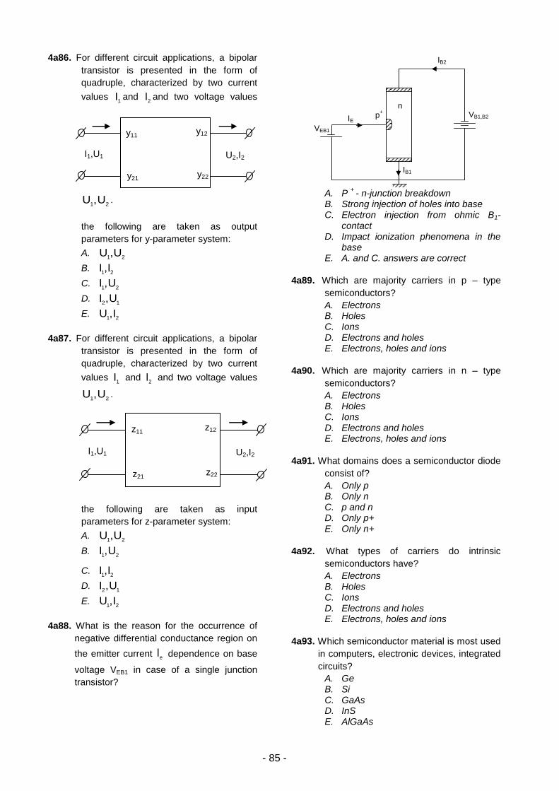
- 85 -
4a86. For different circuit applications, a bipolar
transistor is presented in the form of
quadruple, characterized by two current
values 1I and
2I and two voltage values
21U,U .
the following are taken as output
parameters for y-parameter system:
A. 21
U,U
B. 21I,I
C. 21
U,I
D. 12
U,I
E. 21I,U
4a87. For different circuit applications, a bipolar
transistor is presented in the form of
quadruple, characterized by two current
values 1I and
2I and two voltage values
21U,U .
the following are taken as input
parameters for z-parameter system:
A. 21
U,U
B. 21
U,I
C. 21I,I
D. 12
U,I
E. 21I,U
4a88. What is the reason for the occurrence of
negative differential conductance region on
the emitter current eI dependence on base
voltage VEB1 in case of a single junction
transistor?
A. P
+ - n-junction breakdown
B. Strong injection of holes into base C. Electron injection from ohmic B1-
contact D. Impact ionization phenomena in the
base E. A. and C. answers are correct
4a89. Which are majority carriers in p – type
semiconductors? A. Electrons B. Holes C. Ions D. Electrons and holes E. Electrons, holes and ions
4a90. Which are majority carriers in n – type
semiconductors?
A. Electrons B. Holes C. Ions D. Electrons and holes E. Electrons, holes and ions
4a91. What domains does a semiconductor diode
consist of? A. Only p B. Only n C. p and n D. Only p+ E. Only n+
4a92. What types of carriers do intrinsic
semiconductors have? A. Electrons B. Holes C. Ions D. Electrons and holes E. Electrons, holes and ions
4a93. Which semiconductor material is most used
in computers, electronic devices, integrated
circuits?
A. Ge B. Si C. GaAs D. InS E. AlGaAs
IE
VEB1
VB1,B2 p+
IB1
IB2
n
I1,U1 U2,I2
y11
y21
y12
y22
I1,U1 U2,I2
z11
z21
z12
z22
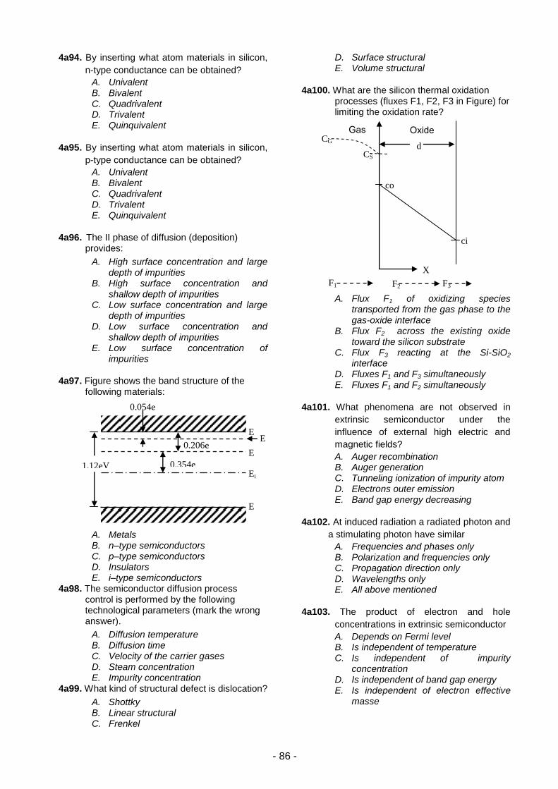
- 86 -
4a94. By inserting what atom materials in silicon,
n-type conductance can be obtained?
A. Univalent B. Bivalent C. Quadrivalent D. Trivalent E. Quinquivalent
4a95. By inserting what atom materials in silicon,
p-type conductance can be obtained?
A. Univalent B. Bivalent C. Quadrivalent D. Trivalent E. Quinquivalent
4a96. The II phase of diffusion (deposition) provides:
A. High surface concentration and large depth of impurities
B. High surface concentration and shallow depth of impurities
C. Low surface concentration and large depth of impurities
D. Low surface concentration and shallow depth of impurities
E. Low surface concentration of impurities
4a97. Figure shows the band structure of the following materials:
A. Metals B. n–type semiconductors C. p–type semiconductors D. Insulators E. i–type semiconductors
4a98. The semiconductor diffusion process control is performed by the following technological parameters (mark the wrong answer).
A. Diffusion temperature B. Diffusion time C. Velocity of the carrier gases D. Steam concentration E. Impurity concentration
4a99. What kind of structural defect is dislocation? A. Shottky B. Linear structural C. Frenkel
D. Surface structural E. Volume structural
4a100. What are the silicon thermal oxidation processes (fluxes F1, F2, F3 in Figure) for limiting the oxidation rate?
A. Flux F1 of oxidizing species
transported from the gas phase to the gas-oxide interface
B. Flux F2 across the existing oxide toward the silicon substrate
C. Flux F3 reacting at the Si-SiO2 interface
D. Fluxes F1 and F3 simultaneously E. Fluxes F1 and F2 simultaneously
4a101. What phenomena are not observed in
extrinsic semiconductor under the
influence of external high electric and
magnetic fields? A. Auger recombination B. Auger generation C. Tunneling ionization of impurity atom D. Electrons outer emission E. Band gap energy decreasing
4a102. At induced radiation a radiated photon and
a stimulating photon have similar
A. Frequencies and phases only B. Polarization and frequencies only C. Propagation direction only D. Wavelengths only E. All above mentioned
4a103. The product of electron and hole
concentrations in extrinsic semiconductor A. Depends on Fermi level B. Is independent of temperature C. Is independent of impurity
concentration D. Is independent of band gap energy E. Is independent of electron effective
masse
Gas CG
CS
co
ci
Oxide
X
F1 F2 F3
d
0.054e
V
0.206e
V 1.12eV 0.354e
V
E
C E
D E
F Ei
E
V
Silicon

- 87 -
4a104. At low temperature range lattice thermal
capacity of a metallic crystal with
temperature increasing
A. Decreases by exponential law B. Increases by exponential law C. Increases by linear law D. Increases by cubic law E. Decreases by linear law
4a105. What is a potential well? A. Energetic state for which a certain
minimum energy is required for the particle to escape it
B. Dimensional space which the particle can escape if acquires maximum energy
C. Limited space where the state energy of the particle is less than its maximum transfer energy
D. Limited space from all sides E. All the answers are correct
4a106. What is quantum tunneling? A. The process of particle transition from
low to high energetic state B. The process of passing particle
through potential barrier when its energy is less than the height of barrier
C. The process when the particle changes its energetic state in potential well
D. The process when the particle moves above potential barrier
E. None of the above
4a107. What is the result of the Schrödinger
equation solution?
A. Time-dependent potential energy of microparticle
B. Coordinate-dependent potential energy of microparticle
C. Probability of microparticle transitioning from potential well
D. Object extension level at some direction
E. Energetic spectrum of microparticle and probability density of microparticle detection at x point of space
4a108. What is quantum phenomenon? A. Dependence of object properties on
dimensions B. Dependence of object properties on
dimensions when object dimensions are equal to de Broglie wavelength at least in one direction
C. Quantization level of microparticle energy dependence on potential well parameters
D. Electron wave interference dependence on the boundary of nanoscale environment division
E. All the answers are correct
4a109. What is superlattice? A. A system of closely distributed
parallel quantum holes between which tunneling is possible
B. A system separated by macroenvironments
C. An environment with quantum dots D. An environment with high density of
quantum states E. A. and B. are correct
4a110. What is the advantage of double
heterojunction lazers conditioned by? A. Occupation of dimensional energetic
levels by charge carriers, injected by direct current
B. Dependence of valence and conduction region edges on x in case of nanoscale-thick active layer
C. Value of active layer refraction index D. Spatial condensation of
nonequilibrium charge carriers in intermediate active layer and their reunion conditioned by increase of radiation intensity
E. Potential barrier transitioning of microparticle with energy lower than barrier
4a111. What processes are involved in the
formation of nonequilibrium
electroconduction in a semiconductor? A. Electron-hole pairs reunion,
accompanying their photogeneration B. Achieving maximum values of the
nonequilibrium electron and hole densities in dynamic balance state
C. Exponential decrease of nonequilibrium charge carrier densities at switching off the light
D. Densities of nonequilibrium charge carriers remain constant after reaching dynamic balance while light exposure is constant
E. All the above mentioned simultaneously
4a112. What is the process of p-n junction barrier
formation conditioned by? A. Diffusion of majority carriers into
opposite region B. Drift of minority carriers C. Enrichment of p-n junction by mobile
charge carriers

- 88 -
D. Formation of p-n junction electrical field
E. All the above mentioned
4a113. The gradual channel approximation for the
MOS transistor’s model is conditioned by:
(Ex is a vertical electric field component in
the channel, Ey is a lateral electric field
component, L – channel length, tox – gate
oxide thickness) A. Ex << Ey B. Ex >> Ey C. EyL = Ex tox D. EyL >> Ex tox E. Eytox = ExL
4a114. What does the gate-substrate
workfunction of a MOS transistor depend
on? A. The gate material and the gate oxide
thickness B. The gate material and the oxide
charge C. The positive or negative bias applied
to the gate electrod D. The gate material and the substrate
doping E. The substrate doping and the electric
field in the channel
4a115. The strong inversion condition for a MOS
transistor model is determined as: A. The energy band curve at the
substrate surface is equal to doubled bulk potential
B. The carrier mobility is constant C. The gate voltage is equal to the flat
band voltage D. The gate-substrate workfunction is
equal to zero E. The bulk potential is greater than 0.8
V 4a116. What kinds of capacitances are there in
SPICE model of MOS transistor?
A. The depletion and diffusion capacitances of the gate – source and the gate – drain p-n junction
B. The overlap gate – source, gate – drain capacitances and the junction capacitances
C. The gate – substrate, the gate – source, the gate – drain and the gate – channel capacitances
D. The gate – substrate, the gate – source, the gate – drain capacitances and the depletion and diffusion capacitances of the gate – source and the gate – drain p-n junction
E. The overlap gate – source, gate – drain capacitances and the parasitic capacitances of the insulating regions
4a117. Calculate the small-signal
transconductance of a bipolar transistor, if
collector current IC = 5,2 mA. A. 5.2 А/V B. 200 mА/V C. 2 mА/V D. 38.5 mА/V E. 520 mА/V
4a118. How does the threshold voltage of an n-
MOS transistor change, if the substrate
bias varies from 0 V to 2 V? The strong
inversion potential PHI = 0,7 V, the body
effect coefficient GAMMA = 0,2 V1/2
. A. Increases at 0.16 V B. Decreases at 0.14 V C. Increases at 0.23 V D. Increases at 0.42 V E. Decreases at 0.26 V
4a119. An NMOS transistor starts to conduct
when: A. The potential difference between the
drain and the source terminals is higher than the threshold voltage Vt
B. The potential difference between the gate and the source terminals is higher than the threshold voltage Vt
C. The potential difference between the gate and the drain terminals is higher than the threshold voltage Vt
D. The potential difference between the drain and the base terminals is higher than the threshold voltage Vt
E. None of the above
4a120. The drain induced barrier lowering
happens because of: A. High gate voltage in an NMOS device B. High drain voltage that contributes in
reducing the threshold voltage C. The decrease in current in the
channel due to high drain voltage D. All of the above E. None of the above
4a121. The static power is affected by many
factors in CMOS ICs, some of these
factors are: A. Temperature, threshold voltage, and
supply voltage B. The activity factor at which the circuit
is switching, supply voltage, and threshold voltage
C. The capacitive load of the circuit, switching activity, and supply voltage

D. The temperature, the switching activity, and the variability in the threshold voltage
E. None of the above
4a122. The basic MOS capacitor in a MOSFET
device is made from A. Gate, Oxide Insulator and
Semiconductor B. Gate, Drain and Source C. Two parallel metal plates D. Gate and Ground E. None of the above
4a123. Compared to BJT’s, the input impedance of a MOSFET transistor is: A. Much smaller B. Much bigger C. About the same value D. Slightly bigger than a typical BJT
device E. None of the above
4a124. In n-channel MOSFET, if large electric
field is applied at the gate, electron
channel build up occurs directly
underneath the semiconductor oxide
layer. This process is called:
A. Accumulation B. Inversion C. Depletion D. Enhancement E. None of the above
4a125. In MOSFETs , the transconductance (gm)
is usually: A. Bigger than a bipolar device B. Smaller than a bipolar device C. Equal to a bipolar device D. The ratio of drain current over drain-
source voltage E. None of the above
4a126. Electron drift current density is given by
EenJnn
, where n is defined as: A. Drift velocity in cm/s B. Electron Mobility in cm
2/V·s
C. Carrier extrinsic concentration in cm -3
D. Conductivity in (Ω·cm)
-1
E. None of the above
4a127. Can an atom function either as donor or as
acceptor in the same material?
A. No B. Yes C. Yes, if the valence is equal to three D. Yes, if the valence is equal to six E. The correct answer is missing
4a128. There is one negative ion on crystal
surface. Which hole will the ion gravitate
to with more power?
A. Hole inside the crystal B. Hole outside the crystal in the same
distance from the surface C. Hole outside the crystal in twice the
distance from the surface D. The correct answer is missing E. All answers are correct
4a129. The crystal thickness is d, the
concentration of free electrons n. How
much will the concentration be if the
crystal thickness is reduced ten times.
A. Will increase ten times B. Will decrease ten times C. Will not change D. Depends only on the width of sample E. Depends only on the length of
sample
4a130. What is the the principle reason of
unsolvability of Shredinger stationary
equation in general form?
A. Lack of a simple mathematical apparatus
B. The problem of many simultaneously interacting particles by quantum theory is in principle unsolvable
C. Number of interacting particles is not a sufficient
D. Particles do not interact with each other.
E. All the answers are correct.
4a131. In crystal having =16 dielectric
transparency due to hole-phonon
interaction, the energy of the hole is
doubled. How many times will the energy
of the hole change if the dielectric
transparency is equal to 1 ( =1)?
A. Will increase sixteen times B. Will reduce sixteen times C. Will remain unchanged D. The question does not make sense E. All the answers are correct.
4a132. Why not just for the conductor, but also for
non degenerate semiconductor,
thermodynamics is the energetic distance
of output operation from Fermi level to
vacuum? In a semiconductor, the Fermi
level lies in the forbidden zone and ther
could be no particle in that level.
A. An electron can leave a semiconductor only from the conductive domain

- 90 -
B. An electron can leave a semiconductor only from the valence domain
C. An electron can leave a semiconductor from both conductive domain and immediately valence domain
D. The correct answer is missing E. All the answers are correct
4a133. What is the value of Fermi energy for
phonon and why?
A. Fermi energy is equal to the bandgap B. Fermi energy is equal to zero C. Fermi energy is equal to half of the
bandgap D. Fermi energy is close to the bottom
of conductivity region E. Fermi energy is close to the top of
conductivity region
4a134. What is the open circuit voltage of
photodiode conditioned by?
A. Diffusion of majority carriers B. Long-wave radiation C. Injection of majority carriers D. Height of potential barrier E. All the answers are correct
4a135. When increasing the intensity of rays, how
will its absorption depnsity change in solid
state?
A. Will increase B. Will decrease C. Will remain the same D. According to spectral range E. The correct answer is missing
4a136. Mainly which noises are decisive in
diodes?
A. Thermal B. Fligerian C. Fractional D. Generation-recombination E. All the mentioned noises
4a137. Which mode of electron motion is called
ballistic?
A. When it moves with finite long wire B. When there are no defects in the
environment C. When the wire length is less than the
electron free run length D. When the diameter of wire cutoff is
less than the electron free run length E. When the last two conditions occur
4a138. What is the potential barriers value of p-n
junction conditioned by?
A. Diffusion of majority carriers from p-and n-domains
B. Fermi level difference of p-and n-domains
C. Ratio of electrons and holes mobility D. The first two E. All the answers are wrong
4a139. The change of which structural parameter
increases the performance of MOS field
transistor?
A. The increase of substrate width B. The decrease of surface of gate
contact C. The decrease of channel length D. The decrease of subgate insulator’s
thickness E. The last two factors
4a140. When is the tunnel effect efficient?
A. When the particle is in a potential hole with great depth
B. When the potential barrier is much larger than the particle’s wavelength
C. When barrier width is comparable to De Broglie wavelength
D. When the energy in not quantized in potential hole
E. All the answers are correct
4a141. In what case is broadband spectral
sensitivity possible in heterojunction
photodiodes?
A. When the ray is absorbed by broadband semiconductor surface
B. When there is great input resistance C. When the ray is absorbed by
narrowband semiconductor surface D. When carriers’ mobility is great E. All the answers are correct
4a142. If a shallow (full ionized) donor
concentration increases twice in an n-type
semiconductor, the concentration of
conduction electrons will
A. Increase twice B. Decrease twice C. Increase more than twice D. Decrease more than twice E. Not change
4a143. Characteristic length for the manifestation
of quantum effects is
A. Electron diffusion length B. Electron free path C. Electron De Broglie wavelength D. Deby screening length E. Lattice constant
4a144. Photon gas is degenerated at
A. Low temperature range B. Very low temperature range
- 91 -
C. High temperature range D. Very high temperature range E. Any temperature range
4a145. In the basics of degenerated and non-
degenerated classification of an electron
gas is the
A. Pauli principle B. Identity principle C. Vegard’s law D. Detailed equilibrium principle E. Heisenberg’s uncertainty principle
4a146. Which of the statements below are false
for the varicap?
A. Work of varicap is based on the phenomenon of the barrier capacitance of the p-n junction
B. Varicap works at forward bias of the p-n junction
C. Varicap capacitance depends on the applied voltage
D. Varicaps are used for the electrical tuning of resonant contours in the circuits
E. Varicap can operate at voltages less than a certain allowable voltages
4a147. Which of the statements below is not
true for stabilitron?
A. Stabilitron is a semiconductor diode, the volt-ampere characteristic of which has a region of sharp dependence of current on voltage at the reverse branch of the characteristics.
B. The differential resistance of an ideal stabilitron in stability region of voltage is close to zero
C. Voltage of stability depends on the physical mechanism of breakdown of the diode
D. For stabilitrons with a a tunneling mechanism of breakdown, the voltage of stability, as a rule, is less than for stabilitrons with avalanche breakdown mechanism
E. Stabilitron is a semiconductor diode, the volt-ampere characteristic of which has a region of current saturation
4a148. To increase the steepness of the
characteristics of the FET, it is
necessary to (which statement is not
true)
A. Reduce the length of the channel and increase its width
B. Reduce the thickness of the gate dielectric
C. Use dielectric with low permittivity
D. For substrate use semiconductor with high mobility of free charge carriers
E. Increase the voltage on the gate of the transistor
4a149. What region is missing in the forward
branch of volt-ampere characteristics of a
diode thyristor?
A. Region of high resistance, corresponding to the close state
B. Region of low resistance, corresponding to the open state
C. Region with negative differential resistance of S-type
D. Direct current region E. Region, not observed in the static volt-
ampere characteristics of a thyristor
4a150. The equation for rds in triode mode
operation using Shichman-Hodges
MOSFET model is the following:
A. 2
*VTOU
L
WKP
gs
dsr
B. 1
VTOUL
WKPr gsds
C.
1
2*
VTOU
L
WKP
gs
dsr
D. W
LKPrds
1
E. VTOUL
WKPr gsds
4a151. The specific contact resistance for the
ohmic contact depends on: A. Contact area B. Substrate doping concentration C. Contact potential difference φk D. All the answers are correct E. The correct answer is missing
4a152. Advantage of Schottky diode over
conventional p-n-junction diode is in:
A. Smaller chip area B. Smaller forward-bias voltage drop at
the same current level C. Smaller reverse-bias current D. All the answers are correct E. The correct answer is missing
4a153. Retrograde well doping distribution is
important for:
A. Decreasing the IC cost B. Suppressing the latch-up effect C. Decreasing the IC chip area D. All the answers are correct E. The correct answer is missing
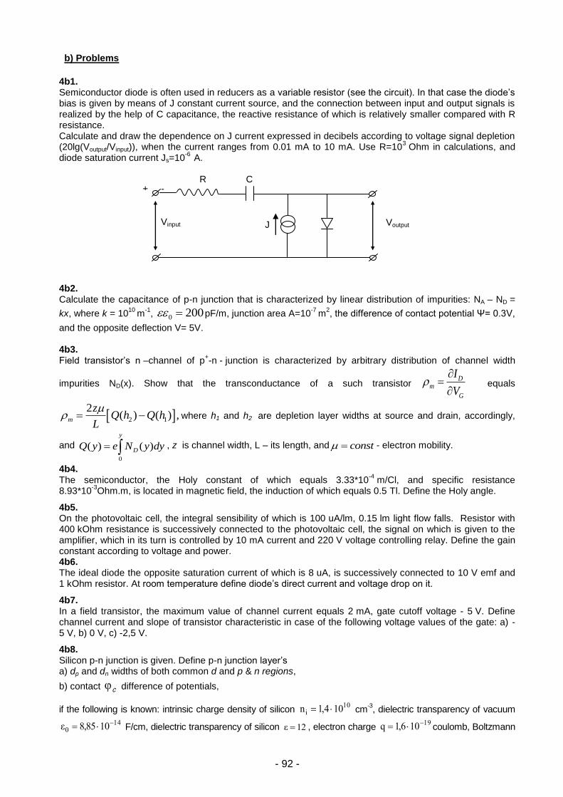
- 92 -
b) Problems
4b1. Semiconductor diode is often used in reducers as a variable resistor (see the circuit). In that case the diode’s bias is given by means of J constant current source, and the connection between input and output signals is realized by the help of C capacitance, the reactive resistance of which is relatively smaller compared with R resistance. Calculate and draw the dependence on J current expressed in decibels according to voltage signal depletion (20lg(Voutput/Vinput)), when the current ranges from 0.01 mA to 10 mA. Use R=10
3 Ohm in calculations, and
diode saturation current Js=10-6
A. 4b2. Calculate the capacitance of p-n junction that is characterized by linear distribution of impurities: NA – ND =
kx, where k = 1010
m-1
, 0 200 pF/m, junction area A=10-7
m2, the difference of contact potential Ψ= 0.3V,
and the opposite deflection V= 5V. 4b3. Field transistor’s n –channel of p
+-n - junction is characterized by arbitrary distribution of channel width
impurities ND(x). Show that the transconductance of a such transistor D
m
G
I
V
equals
2 1
2( ) ( ) ,m
zQ h Q h
L
where h1 and h2 are depletion layer widths at source and drain, accordingly,
and
0
( ) ( )
y
DQ y e N y dy , z is channel width, L – its length, and const - electron mobility.
4b4. The semiconductor, the Holy constant of which equals 3.33*10
-4 m/Cl, and specific resistance
8.93*10-3
Ohm.m, is located in magnetic field, the induction of which equals 0.5 Tl. Define the Holy angle.
4b5. On the photovoltaic cell, the integral sensibility of which is 100 uA/lm, 0.15 lm light flow falls. Resistor with 400 kOhm resistance is successively connected to the photovoltaic cell, the signal on which is given to the amplifier, which in its turn is controlled by 10 mA current and 220 V voltage controlling relay. Define the gain constant according to voltage and power. 4b6. The ideal diode the opposite saturation current of which is 8 uA, is successively connected to 10 V emf and 1 kOhm resistor. At room temperature define diode’s direct current and voltage drop on it.
4b7. In a field transistor, the maximum value of channel current equals 2 mA, gate cutoff voltage - 5 V. Define channel current and slope of transistor characteristic in case of the following voltage values of the gate: a) -5 V, b) 0 V, c) -2,5 V.
4b8. Silicon p-n junction is given. Define p-n junction layer’s a) dp and dn widths of both common d and p & n regions,
b) contact c difference of potentials,
if the following is known: intrinsic charge density of silicon 10
i 104,1n cm-3, dielectric transparency of vacuum
140 1085,8 ε F/cm, dielectric transparency of silicon 12ε , electron charge
19106,1q coulomb, Boltzmann
+ -
Voutput Vinput
C
J
R
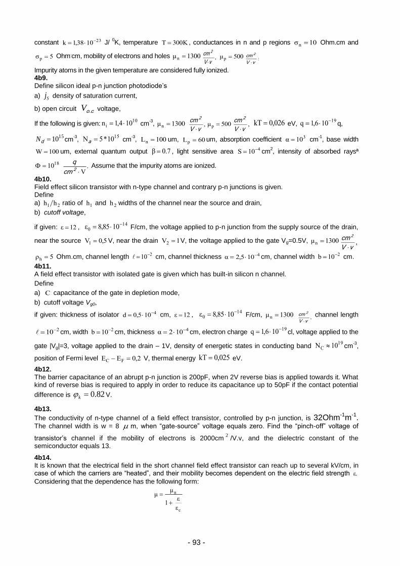
- 93 -
constant 231038,1k J/ 0K, temperature K300T , conductances in n and p regions 10n σ Ohm.cm and
5p σ Ohm.cm, mobility of electrons and holes 1300n μ ,
v V
cm 2
500p μ :
v V
cm 2
Impurity atoms in the given temperature are considered fully ionized. 4b9. Define silicon ideal p-n junction photodiode’s
a) Sj density of saturation current,
b) open circuit o.cV voltage,
If the following is given:10
i 104,1n cm-3, 1300n μ ,
v V
cm 2
500p μ ,
v V
cm 2
026,0kT eV,
19106,1q q,
1510dN cm-3,
1510*5N a cm-3, 100Ln um, 60Lp um, absorption coefficient 310α cm
-1, base width
100W um, external quantum output 7.0β , light sensitive area 410S cm2, intensity of absorbed raysª
1810 .V2cm
q
Assume that the impurity atoms are ionized.
4b10. Field effect silicon transistor with n-type channel and contrary p-n junctions is given. Define
a) 21 hh ratio of 1h and 2h widths of the channel near the source and drain,
b) cutoff voltage,
if given: 12ε , 14
0 1085,8 ε F/cm, the voltage applied to p-n junction from the supply source of the drain,
near the source 5,0V1 V, near the drain 1V2 V, the voltage applied to the gate Vg=0.5V, 1300n μ ,v V
cm 2
5h ρ Ohm.cm, channel length 210 cm, channel thickness 4105,2 α cm, channel width 210b cm.
4b11. A field effect transistor with isolated gate is given which has built-in silicon n channel.
Define
a) C capacitance of the gate in depletion mode,
b) cutoff voltage Vg0,
if given: thickness of isolator 4105,0d cm, 12ε , 14
0 1085,8 ε F/cm, 1300n μ ,v V
cm 2
channel length
210 cm, width 210b cm, thickness 4102 α cm, electron charge 19106,1q cl, voltage applied to the
gate |Vg|=3, voltage applied to the drain – 1V, density of energetic states in conducting band 19
C 10N cm-3,
position of Fermi level 2,0EE FC V, thermal energy 025,0kT eV.
4b12. The barrier capacitance of an abrupt p-n junction is 200pF, when 2V reverse bias is applied towards it. What kind of reverse bias is required to apply in order to reduce its capacitance up to 50pF if the contact potential
difference is 82.0k V.
4b13.
The conductivity of n-type channel of a field effect transistor, controlled by p-n junction, is 32Ohm-1m-1. The channel width is w = 8 m, when “gate-source” voltage equals zero. Find the “pinch-off” voltage of
transistor’s channel if the mobility of electrons is 2000cm2
/V.v, and the dielectric constant of the semiconductor equals 13.
4b14. It is known that the electrical field in the short channel field effect transistor can reach up to several kV/cm, in case of which the carriers are “heated”, and their mobility becomes dependent on the electric field strength ε.
Considering that the dependence has the following form:
c
n
1ε
ε
μμ
- 94 -
( nμ - low field mobility of electrons, cε -critical value of electrical field) find the drain current dependence on
its and the gate’s voltages. Also consider that the channel length, width and depth are given.
4b15.
Boron diffusion is provided from a “limited source” with the total amount of impurities 131025,2 Q atom/cm
2
in 2t hour. Diffusion coefficient equals 13102,9 D cm2/s. Diffusion is provided into the bulk silicon
substrate with the impurity concentration 16101DN atom/cm
3. Calculate the depth of p-n junction jx in
micrometers. 4b16.
Consider a pnp silicon transistor with doping levels of emitter, base and collector AEN = 18105 cm
-3,
DBN = 1610 cm3, AKN = 1510 cm
3, base width 1W m, cross sectional area is 3 mm2, and applied
voltages are 5.0UEB V, 5UBK V. Calculate the width of quasi-neutral part of the base, minority carriers’
(holes) concentration near the emitter-base junction and total charge of minority carriers injected into the base (T=300K).
4b17. Calculate the bipolar diffusion coefficient of current carriers in intrinsic GaAs at 300K if electron and hole mobilities are equal 8800cm
2/V.s and 400cm
2/V.s, correspondingly.
4b18. Find the potential barrier’s height existing for electrons in Schottky diode if the specific resistance of a
semiconductor 1 Om cm , electrons’ mobility 3900 2 /cm V s , gold work function Auφ 5 eV ,
semiconductor’s electron affinity ` Geχ 4 eV , intrinsic concentration 13
i 105.2n cm3
, band-gap width
gE 0.66 eV (T=300K).
4b19. For an ideal p-n-p transistor, the current components are given by Iep=3mA, Ien=0.01mA, Icp=2.99mA, Icn=0.001mA. Determine:
a) The emitter efficiency (), b) The base transport coefficient (lT), c) The common-base current gain È0 and IcB0. 4b20. In n-channel n
+-multicrystal Si-SiO2-Si MOS transistor Na=10
17cm
-3, (Qox/Q)=5*10
11cm
-2, calculate the
threshold voltage VT, if the oxide layer thickness is 5nm. What density of Bor ions is necessary to increase the threshold voltage up to 0.6V?
2B=0.84V, Si02=3.9, S=-0.98V, Si=11.9. 4b21. Intrinsic Ge is in 3000 K temperature. How many percent will the specific conductance of the sample change if the temperature increases by 1%. Accept 4b22.
Given mobilities of electrons and holes pn μμ ¨ , find the concentration of charge carriers corresponding
to minimal specific conductance.
4b23. How will charge carrier’s lifetime in non-generated semiconductor change under the doped impurity concentration if it is known that T =3000K is constant, the mobility increases by 5%, and diffusion length decreases by 10 %? 4b24. Using hydrogen atom model, calculate in semiconductor InSb crystal a) donors’ ionization energy, b) the radius of electrons in basic state, c) the electron concentration density T = 4
o K, when Nd = 1. 1014 cm
-3.
The radius of basic orbits is ,53.0o
H Ar and bandgap of InSb Eg = 0.18eV,
oos mmm (,014.0,17 * is free electron mass), 0258.0kT eV when T = 300 K, and ionization
energy HE = 13.6 eV.
- 95 -
4b25. What number of electrons must pass from one metal to another for Vk=1V contact potential difference to
occur between them when the width of dielectric between metals is d=10-9
m, 141085.8 o F/cm.
Compare the amount when there is metal-n type semiconductor contact for the same condition when in the
surface of metal, concentration of electrons is 2510smn c
-2, and in semiconductor
1010ssn cm-2
.
4b26. A (n - p - n) transistor circuit connected by general emitter is shown. Calculate, according to power,
amplification coefficient if 20,98.0 er Ohm, 500br Ohm, 30LR kOhm.
4b27.
In an intrinsic semiconductor electron concentration is 16103.1 cm
-3 at 400K and
15102.6 cm-3
at 350K.
Determine the forbidden band gap of material if it changes linearly via temperature.
4b28. Determine the holes distribution in the n-type thin and long non-degenerated germanium wire in the case of
point stationary injection of holes at point 0x . Electric field intensity applied on the sample is 5E V/cm,
temperature is 300T K, hole diffusion length is 09.0Lp cm.
4b29.
From the plane 0x of homogeneous half-infinite ( 0x ) n-type semiconductor injected holes are
stationary. Determine hole current density at x=0 point if 1310)0(p cm
-3, hole diffusion length is 07.0Lp
cm, hole diffusion coefficient is 49Dp cm2/s, injection coefficient is 4.0ξ . Non-equilibrium carrier drift is
neglected. 4b30. The N type silicon sample has 4mm length, 1,5mm width, 1mm hight and 80 Ohm resistivity. Determine the acceptor concentration of the sample if 0.12m
2/Vc and 0.025m
2/Vc are the electron and hole mobilities,
respectively, 2.51016
m-3
is the intrinsic concentration of current carrier. 4b31. In the photodetector by surface p-n junction, the width of active layer, creating photocurrent, is d=1um,
F=1014
quantum/cm2s, by α = 10
4cm
-1 and α = 10
3cm
-1 absorption coefficients, double wave (1 and 2)
radiation (hEg) are absorbed by photosensitive surface. Calculate the photocurrent ratio, created by those
two wave absorption if photosensitive area is S = 10-4 cm
2, quantum output =1, electron charge q=1.6
.10
-19c.
4b32. Define the performance of photodiode if volume charge layer width is d=10
-4 cm, maximum speed of carriers’
movement Vmax = 5.10
6 cm/s, electron density in n-type base n = 5
.10
15cm
-3, mobility n = 1,3
.10
3 cm
2/V
.s,
diffusion coefficient of minority carriers - holes Dp= 15,6 cm2/v, Holes mobility in base p = 600 cm
2/Vv,
electron charge q = 1.6.10
-19c, base width w = 3
.10
-3cm, photosensitive area S = 10
-2 cm
2, dielectric
permeability of semiconductor = 12, vacuum 0 = 8.8610-14
f/cm.
4b33. Define power density equivalent to photodiode noise if dark and light current sum I=Id+IL=5,1
.10
-7A,
frequency band Δf =1Hz, absorption radiation power P = 10-6
Vt, photocurrent IÈ=5.10
-7A, photosensitive
surface S = 10-2
cm2, electron charge q = 1.6
.10
-19c.
4b34. Define channel width shrinkage through p-n junction at the drain of field transistor, when source-drain domain affects are missing, V=+0.5 V voltage has been applied to the drain, dielectric permeability of
channel material =12, vacuum 0=8.8610-14
f/cm, contact difference of potentials =0.7V, donors’ density in and n-channel Nd=5
.10
14cm
-3, electron charge q = 1.6
.10
-19c.
bi ci
ei gr LR
Input
output

- 96 -
4b35 Calculate the drain current of an NMOS Si transistor according to the following conditions: threshold voltage Vt=1 V, gate width W=10 µm, gate length L=1 µm, thickness of oxide layer tox=10 nm, VGS=3 V and VDS=5 V. For calculation, use square model, surface mobility is 300 cm
2/V and VBS=0 V. Also calculate gm
transconductance.
4b36
Define the space charge, the values of Qsc charge and Csc capacity for the following values of ϕs surface
potential: ϕs=0; ϕs= ϕ0; ϕs=2ϕ0, for p- type of the silicon, ρsi=10 Om·cm, µn=1500 cm2/V·sec, µp=600
cm2/V·sec, εs=11.8, ε0=8.85·10
-14 F/cm, ni=1.6·10
10 cm
-3.
4b37. Define the surface-state charge density Qss for p- type silicon Na=10
18 cm
-3, T=300 K, according to the
following values of surface potential: ϕs=0; ϕs= ϕ0; ϕs=2ϕ0. Surface states are evenly distributed Nss=2·1012
cm
-2·eV
-1. Compare the value of Qss with the appropriate charge of surface-state charge Qsc. ε0=8.85·10
-14
F/cm, εs=11.8, ni=1.6·1010
cm-3
.
4b38. The density of donor in semiconductor which contains only donor impurity, is Nd, and their energy level is Ed. Find out the density of free electrons if the Fermi level coincides with Ed. 4b39. Under the influence of light, homogenous distributed exceed charge carriers with the concentration of Δn occurred in semiconductor. The density of minority charge carriers is 2.5·10
20 m
-3, and initial speed
decrease of the density is 2.8·1024
m-3
·sec-1
. Define:
a. The lifetime of minority charge carriers;
b. The value of Δn after 2 µsec when the light source had already been turned off.
4b40. The mobility of electrons is 0.38 m
2/V·sec in the germanium sample, and the mobility of holes is 0.16
m2/V·sec. The Holy effect is not seen in this sample. Which part of the current is conditioned by holes?
4b41. As the concentration of impurity has changed, the mobility increased by 5% in non-degenerate semiconductor at constant temperature T=300 K, and diffusion length increased by 10%. How did the lifetime of charge carriers change? 4b42. The concentration of donors is Nd=2·10
20 m
-3 in germanium sample. The effective mass of electron is
m*=1.57m0 (m0 is electron mass in vacuum). It can be considered that donor is dispersive center with 5·10
-2
µm of radius. Find out the mean free path and time as well as electron mobility if T=300 K.
4b43.
For the InSb crystal 23.0Eg is the forbidden gap, 17 is the dielectric permittivity, 0m015.0m is the
electron effective mass. Determine the minimal concentration of donors when impurity band is originated.
4b44.
In the silicon with 300K temperature electron mobility is 1500μ cm2/Vc and electron effective mass is
0m32.0m . Determine the electric field when band-to-band impact ionization takes place.
4b45. Determine the coefficient of temperature expansion of semiconductor forbidden gap, if the product of
electron and hole effective mass equals 0m235.0 , intrinsic carriers’ concentration equals 16102 cm-3
at
K500T1 and 12108 cm-3
at K280T2 .
4b46.
Determine the energy of electron that is reflected from the atomic (100) planes of the cubic crystalline
lattice with constant o
Aa 4 when the reflection angle is o45 .
4b47.
Find silicon photodiode’s idle state voltage if the radiation with 18
010F
scm
qv2
intensity is observed in the
active region of p-n junction. The external quantum output is 1, reflection coefficient 0. Electron and hole
- 97 -
mobility equal 1300n ,v V
cm2
500p μ
v V
cm2
respectively, diffusion length of minority carriers
210nL
cm, 3
p 10*6L cm, electron charge 19106,1q K, thermal energy 026,0kT eV. Also given densities of
majority carriers in n and p domains 1510 ap Np cm
-3,
15dn 10*5Nn cm
-3, density of intrinsic charge
10ii 10*4.1pn cm
-3:
4b48.
Given silicon p-n junction. The position of Fermi level in n region is 2,0 FC EE eV, and in p region it is
1,0 VF EE eV. Density of energetic states in conductance and valence regions 1910*8.2CN cm
-3,
1910*02.1VN cm-3
. Also given intrinsic carriers’ density in a silicon 1010*6.1 ii pn cm
-3 and room
temperature energy 026,0kT eV. Define the contact difference of p-n junction potentials.
4b49. Define the charge capacitance of silicon structure of two backward potential barriers if the depletion layers have symmetric distribution and contact edge. The total width of depletion layers d=10
-4 cm, and the area of
p-n junction S 10-4
cm2. Accept the dielectric transparency of vacuum 0 = 8.86 10
-12 F/m, and the one of
Si = 12.
4b50. Barrier capacitance of p-n junction is C1 = 100 pF for 2V backward bias voltage. What value will the
capacitance take in case of decreasing V voltage twice? The height of potential barrier of p-n junction is = 0.6V.
4b51. Determine Miller indices of the shaded plane in a cubic crystal.
4b52. n-type silicon has the following sizes: length is 10mm, width is 2mm and thickness is 1mm. Mobilities for
electron and hole are 0.12 and 0.05m2/(V-s) respectively. The intrinsic carrier density is
161.5 10in m-3
and the elementary charge is191.6 10q C. Determine the donor impurities concentration Nd in the
substrate when the resistance is R=150 . 4b53. Prove that semiconductor at the given temperature has minimum conductivity if the electron density is
/i p nn n . Here n and in are intrinsic densities and p and n are hole and electron motilities
respectively. 4b54.
Conductivities of p and n regions for germanium p-n-junction are 410p 1( )m and
210n 1( )m
respectively. Electron and hole mobilities are 0.39 and 0.19m2/ (V-s), intrinsic carrier density is
192.5 10in
m-3
and elementary charge is 191.6 10q C.
Calculate the diffusion potential at T=300k.
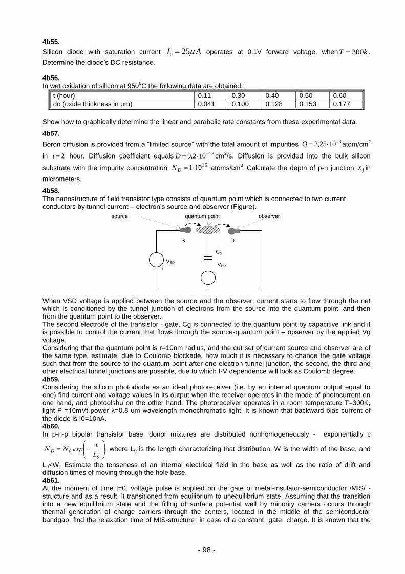
- 98 -
4b55.
Silicon diode with saturation current 0 25I A operates at 0.1V forward voltage, when 300T k .
Determine the diode’s DC resistance. 4b56. In wet oxidation of silicon at 950
0C the following data are obtained:
t (hour) 0.11 0.30 0.40 0.50 0.60
do (oxide thickness in µm) 0.041 0.100 0.128 0.153 0.177
Show how to graphically determine the linear and parabolic rate constants from these experimental data.
4b57.
Boron diffusion is provided from a “limited source” with the total amount of impurities 131025,2 Q atom/cm
2
in 2t hour. Diffusion coefficient equals 13102,9 D cm2/s. Diffusion is provided into the bulk silicon
substrate with the impurity concentration 16101DN atoms/cm
3. Calculate the depth of p-n junction jx in
micrometers.
4b58. The nanostructure of field transistor type consists of quantum point which is connected to two current conductors by tunnel current – electron’s source and observer (Figure). When VSD voltage is applied between the source and the observer, current starts to flow through the net which is conditioned by the tunnel junction of electrons from the source into the quantum point, and then from the quantum point to the observer. The second electrode of the transistor - gate, Cg is connected to the quantum point by capacitive link and it is possible to control the current that flows through the source-quantum point – observer by the applied Vg voltage. Considering that the quantum point is r=10nm radius, and the cut set of current source and observer are of the same type, estimate, due to Coulomb blockade, how much it is necessary to change the gate voltage such that from the source to the quantum point after one electron tunnel junction, the second, the third and other electrical tunnel junctions are possible, due to which I-V dependence will look as Coulomb degree. 4b59. Considering the silicon photodiode as an ideal photoreceiver (i.e. by an internal quantum output equal to one) find current and voltage values in its output when the receiver operates in the mode of photocurrent on one hand, and photoelshu on the other hand. The photoreceiver operates in a room temperature T=300K, light P =10mVt power λ=0,8 um wavelength monochromatic light. It is known that backward bias current of the diode is I0=10nA. 4b60. In р-n-р bipolar transistor base, donor mixtures are distributed nonhomogeneously - exponentially c
00D
L
xexpNN , where L0 is the length characterizing that distribution, W is the width of the base, and
L0<W. Estimate the tenseness of an internal electrical field in the base as well as the ratio of drift and diffusion times of moving through the hole base. 4b61. At the moment of time t=0, voltage pulse is applied on the gate of metal-insulator-semiconductor /MIS/ - structure and as a result, it transitioned from equilibrium to unequilibrium state. Assuming that the transition into a new equilibrium state and the filling of surface potential well by minority carriers occurs through thermal generation of charge carriers through the centers, located in the middle of the semiconductor bandgap, find the relaxation time of MIS-structure in case of a constant gate charge. It is known that the
-
VSD
+
Cg VSD
source quantum point observer
S D
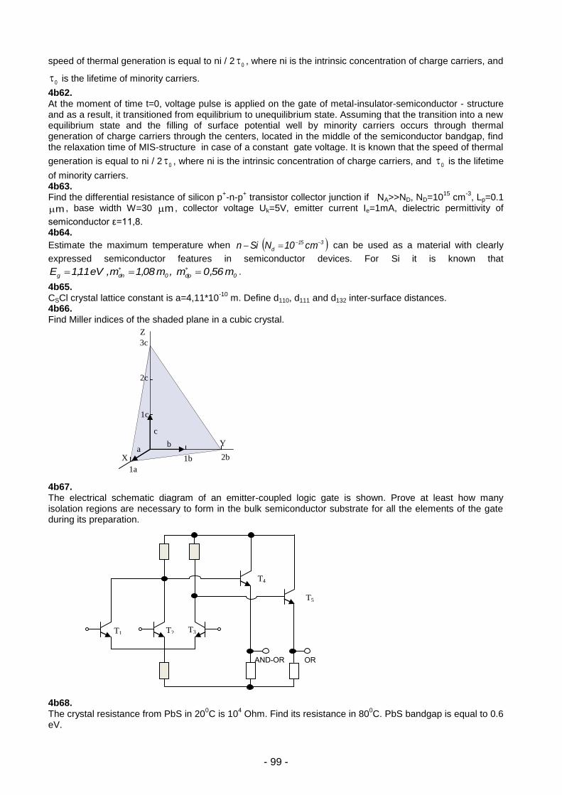
- 99 -
speed of thermal generation is equal to ni / 20 , where ni is the intrinsic concentration of charge carriers, and
0 is the lifetime of minority carriers.
4b62. At the moment of time t=0, voltage pulse is applied on the gate of metal-insulator-semiconductor - structure and as a result, it transitioned from equilibrium to unequilibrium state. Assuming that the transition into a new equilibrium state and the filling of surface potential well by minority carriers occurs through thermal generation of charge carriers through the centers, located in the middle of the semiconductor bandgap, find the relaxation time of MIS-structure in case of a constant gate voltage. It is known that the speed of thermal
generation is equal to ni / 20 , where ni is the intrinsic concentration of charge carriers, and
0 is the lifetime
of minority carriers. 4b63. Find the differential resistance of silicon p
+-n-p
+ transistor collector junction if NA>>ND, ND=10
15 cm
-3, Lp=0.1
m , base width W=30 m , collector voltage Uk=5V, emitter current Ie=1mA, dielectric permittivity of
semiconductor ε=11,8. 4b64.
Estimate the maximum temperature when 315
d cm10NSin can be used as a material with clearly
expressed semiconductor features in semiconductor devices. For Si it is known that
0dp0dng m56,0m,m08,1m,eV11,1E .
4b65. CSCl crystal lattice constant is a=4,11*10
-10 m. Define d110, d111 and d132 inter-surface distances.
4b66. Find Miller indices of the shaded plane in a cubic crystal.
4b67. The electrical schematic diagram of an emitter-coupled logic gate is shown. Prove at least how many isolation regions are necessary to form in the bulk semiconductor substrate for all the elements of the gate during its preparation.
4b68. The crystal resistance from PbS in 20
0C is 10
4 Ohm. Find its resistance in 80
0C. PbS bandgap is equal to 0.6
eV.
2c
1c
a X
1a
1b 2b
Y
Z
3c
c
b
AND-OR OR
T1 T2 T3
T4
T5
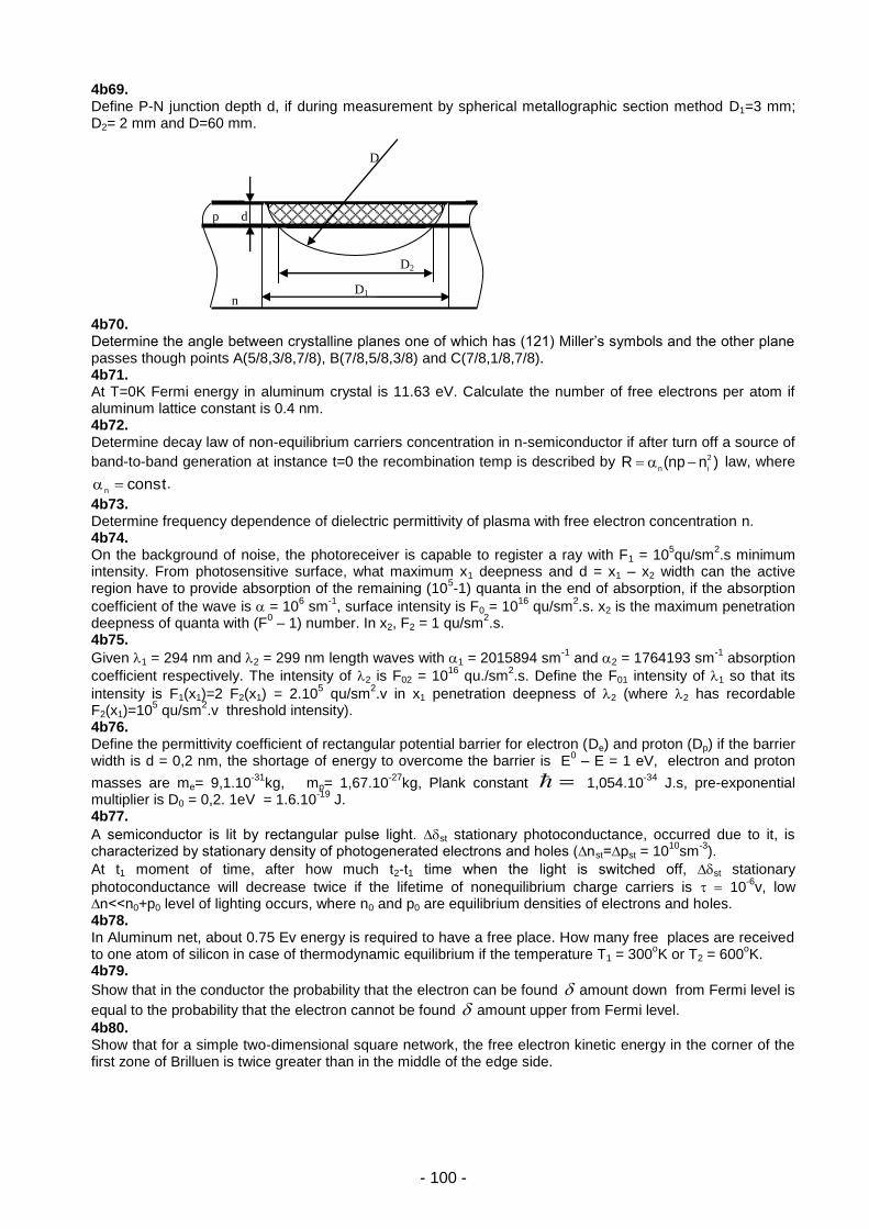
- 100 -
4b69. Define P-N junction depth d, if during measurement by spherical metallographic section method D1=3 mm; D2= 2 mm and D=60 mm.
4b70. Determine the angle between crystalline planes one of which has (121) Miller’s symbols and the other plane passes though points A(5/8,3/8,7/8), B(7/8,5/8,3/8) and C(7/8,1/8,7/8). 4b71. At T=0K Fermi energy in aluminum crystal is 11.63 eV. Calculate the number of free electrons per atom if aluminum lattice constant is 0.4 nm. 4b72. Determine decay law of non-equilibrium carriers concentration in n-semiconductor if after turn off a source of
band-to-band generation at instance t=0 the recombination temp is described by )nnp(R 2
in law, where
constn .
4b73. Determine frequency dependence of dielectric permittivity of plasma with free electron concentration n. 4b74. On the background of noise, the photoreceiver is capable to register a ray with F1 = 10
5qu/sm
2.s minimum
intensity. From photosensitive surface, what maximum x1 deepness and d = x1 – x2 width can the active region have to provide absorption of the remaining (10
5-1) quanta in the end of absorption, if the absorption
coefficient of the wave is = 106 sm
-1, surface intensity is F0 = 10
16 qu/sm
2.s. x2 is the maximum penetration
deepness of quanta with (F0 – 1) number. In x2, F2 = 1 qu/sm
2.s.
4b75.
Given 1 = 294 nm and 2 = 299 nm length waves with 1 = 2015894 sm-1
and 2 = 1764193 sm-1
absorption
coefficient respectively. The intensity of 2 is F02 = 1016
qu./sm2.s. Define the F01 intensity of 1 so that its
intensity is F1(x1)=2 F2(x1) = 2.105 qu/sm
2.v in x1 penetration deepness of 2 (where 2 has recordable
F2(x1)=105 qu/sm
2.v threshold intensity).
4b76. Define the permittivity coefficient of rectangular potential barrier for electron (De) and proton (Dp) if the barrier width is d = 0,2 nm, the shortage of energy to overcome the barrier is E
0 – E = 1 eV, electron and proton
masses are me= 9,1.10-31
kg, mp= 1,67.10-27
kg, Plank constant 1,054.10-34
J.s, pre-exponential multiplier is D0 = 0,2. 1eV = 1.6.10
-19 J.
4b77.
A semiconductor is lit by rectangular pulse light. ∆st stationary photoconductance, occurred due to it, is characterized by stationary density of photogenerated electrons and holes (∆nst=∆pst = 10
10sm
-3).
At t1 moment of time, after how much t2-t1 time when the light is switched off, ∆st stationary
photoconductance will decrease twice if the lifetime of nonequilibrium charge carriers is 10-6
v, low ∆n<<n0+p0 level of lighting occurs, where n0 and p0 are equilibrium densities of electrons and holes. 4b78. In Aluminum net, about 0.75 Ev energy is required to have a free place. How many free places are received to one atom of silicon in case of thermodynamic equilibrium if the temperature T1 = 300
oK or T2 = 600
oK.
4b79.
Show that in the conductor the probability that the electron can be found amount down from Fermi level is
equal to the probability that the electron cannot be found amount upper from Fermi level.
4b80. Show that for a simple two-dimensional square network, the free electron kinetic energy in the corner of the first zone of Brilluen is twice greater than in the middle of the edge side.
D2
D1
D
p d
n
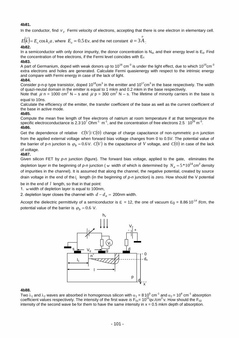
- 101 -
4b81.
In the conductor, find F Fermi velocity of electrons, accepting that there is one electron in elementary cell.
akEkE xo cos , where 5.0oE Ev, and the net constant
o
Aa 3 :
4b82. In a semiconductor with only donor impurity, the donor concentration is Nd, and their energy level is Ed. Find
the concentration of free electrons, if the Fermi level coincides with Ed.
4b83. A part of Germanium, doped with weak donors up to 10
16 cm
-3 is under the light effect, due to which 10
15cm
-3
extra electrons and holes are generated. Calculate Fermi quasienergy with respect to the intrinsic energy and compare with Fermi energy in case of the lack of light. 4b84. Consider p-n-p type transistor, doped 10
18cm
3 in the emitter and 10
17cm
3 in the base respectively. The width
of quazi-neutal domain in the emitter is equal to 1 mkm and 0.2 mkm in the base respectively. Note that n = 1000 cm
2 N – s and p = 300 cm
2 N – s. The lifetime of minority carriers in the base is
equal to 10ns. Calculate the efficiency of the emitter, the transfer coefficient of the base as well as the current coefficient of the base in active mode. 4b85. Compute the mean free length of free electrons of natrium at room temperature if at that temperature the specific electroconductance is 2.3
.10
7 Ohm
-1 . m
-1, and the concentration of free electrons 2.5
. 10
28 m
-3.
4b86.
Get the dependence of relative 0/ CVC change of charge capacitance of non-symmetric p-n junction
from the applied external voltage when forward bias voltage changes from 0 to 0.5V. The potential value of
the barrier of p-n junction is 6.0b V. VC is the capacitance of V voltage, and 0C in case of the lack
of voltage. 4b87. Given silicon FET by p-n junction (figure). The forward bias voltage, applied to the gate, eliminates the
depletion layer in the beginning of p-n junction ( w width of which is determined by 1410*5aN cm
3 density
of impurities in the channel). It is assumed that along the channel, the negative potential, created by source
drain voltage in the end of the1l length (in the beginning of p-n junction) is zero. How should the V potential
be in the end of l length, so that in that point:
1. w width of depletion layer is equal to 100nm,
2. depletion layer closes the channel with ndd 200nm width.
Accept the dielectric permittivity of a semiconductor is = 12, the one of vacuum 0 = 8.8610-14
f/cm, the
potential value of the barrier is 6.0b V.
4b88.
Two 1 and 2 waves are absorbed in homogenous silicon with 1 = 8.10
5 cm
-1 and 2 = 10
6 cm
-1 absorption
coefficient values respectively. The intensity of the first wave is F01= 1015
qv./cm2.v. How should the F02
intensity of the second wave be for them to have the same intensity in x = 0.5 mkm depth of absorption.
s
Vl
V2
hv
Vg g d
0
dn
- - +
n+
l1
l
p d
x

- 102 -
4b89. Find the drift length of non-equilibrium holes in n- Si for T = 300K when the electric field tension is E = 10 V/cm, and the length of holes diffusion is Lp = 1.5
.10
-2 cm. kT = 0.025 Ev.
4b90.
A silicon p-n junction is initially biased at 0.60 V at T = 300 K, 1/ TkeV B . Assume the temperature
increases to T = 310 K. Calculate the change in the forward-bias voltage required to maintain a constant current through the junction. 4b91.
For the electron gas with concentration n at 0T temperature, determine the average kinetic energy of
the electron with m mass.
4b92.
Holes are injected from plane 0x of long ( 0x ) and non-degenerate n type semiconductor. Determine
the distribution of steady-state excess hole concentration as a function of x when applied electric field is 8
V/cm; T= 300K, hole diffusion length is 04.0 cm. 4b93. GaAs bulk material fabricated for the estimation of Hall-effect has dimensions dx =0.5 mm, dy=3mm, and dz=10mm. The electric current is Ix=5 mA, the bias voltage is Vx=2.5 V, and the magnetic field is B=Bz =0.1 T. The Hall voltage was measured to be VH = −3.0 mV. Calculate the majority carrier mobility and the conductance. What is the conductivity type? 4b94. Avalanche photodiode has a multiplication coefficient M = 20 at a wavelength of λ = 1.5mkm. The sensitivity of the photodiode at this wavelength is equal to R = 0.6 A/W, when the photon flux is rp=10
10 photon/s.
Calculate the quantum yield and the output photocurrent. 4b95.
At the surface of n-Si (ND =1016
cm-3
) at the value of the surface potential 02 S , where e
EE iF 0 (
0e - distance from the Fermi level to the center of the bandgap), a triangular potential well is formed in
which the spectrum of heavy holes is quantized. Find the total number of two-dimensional holes in the first subband at T = 77K. 4b96.
The silicon transistor of n+-p- n type has the effectiveness of an emitter =0.999, transfer coefficient through
the base т=0.99, the thickness of the neutral base region Wb = 0.5 um, the concentration of impurities in the emitter ND=5*10
19cm
-3 , in the base NA=10
16см
-3 , and in the colelctor - ND=5*10
15см
-3. Determine the
threshold voltage on the emitter, at which the device ceases to be controlled and the puncture occurs. Calculate transit time through the base and the cutoff frequency. 4b97. For what value of the voltage on metal electrode the flat-band condition is established in the p-type semiconductor of MOS structure, if the work function difference of the metal and semiconductor is equal to
φm/p, the charge on the surface states is Qss, and the specific capacitance of the dielectric layer - Cox. 4b98. Calculate n-MOSFET channel depletion layer width in strong inversion mode if substrate bias is Vbs=0 and -2V; substrate doping concentration in the channel region is Nb=10
16 cm
-3.
Additional data for calculation: T=300K; Si-substrate; φt=25.8 mV; ni=1.5∙1010
cm-3
; ε∙ ε 0 = 1.1 pF/cm; e =1.6∙10
-19 C.
4b99. Estimate the width and the length of a square annular NMOS transistor.
Gate geometry for square annular NMOS transistor.
b
a

- 103 -
4b100. Calculate the zero-bias junction capacitance Cj(0) for abrupt p-n junction. The doping density of the n-type region is ND = 10
20 cm
-3, the doping density of the p-type region is NA=10
16cm
-3. The junction area is
S=1.5um x 1.5 um. 4b101. Determine the type of die (core-limited or pad-limited) if the total cell area equals 49 mm
2, the total number of
pads NP is 128, the width of pad WP equals 100 um and the minimum spacing between adjacent pads SP is 100 um.

- 104 -
5. SEMICONDUCTOR TECHNOLOGY
a) Test questions 5a1. What is the number of photomasks
defined by during the fabrication of the given integrated circuit? A. Photomask wearability B. Number of simultaneously processing
semiconductor wafers C. Number of topological layers formed
on the wafer D. Minimum of feature size E. Production volume
5a2. What semiconductor material has the maximum band gap? A. Si B. Ge C. GaAs D. SiC E. The correct answer is missing
5a3. The performance of a MOS transistor can be increased by: A. Increasing the temperature B. Decreasing the temperature C. Changing the channel doping level D. Decreasing thickness of dielectric
layer E. Increasing the gate voltage
5a4. Based on what semiconductor is it possible to make p-n junctions having higher operating temperatures? A. Ge, Eg=0,66 eV B. Si, Eg=1,12 eV C. GaAs, Eg=1,45 eV D. SiC, Eg= 3,1 eV E. The correct answer is missing
5a5. The best resolution to form a topological pattern is A. X-ray lithography B. Electron beam lithography C. Photolithography D. Chemical lithography E. All the answers are correct
5a6. What kind of p-n junction can be produced by epitaxial technology? A. Linearly graded p-n junction B. p-n junction by exponent function C. Abrupt p-n junction D. All the answers are correct E. The correct answer is missing
5a7. Operating frequency of bipolar transistors can be increased by A. Increasing emitter effectiveness B. Decreasing base width C. Applying collector large voltages D. Decreasing base impurity level E. Increasing signal frequency
5a8. Charge capacitance is larger than diffusion A. Because it does not depend on the
frequency B. In reverse-biased mode of p-n
junction, C. In forward-biased mode of p-n
junction D. Because it depends on the value of
applied voltage E. Because it depends on the value of
current
5a9. p-n junction current in reverse-biased mode can be reduced by: A. The reduction of the density of
impurities B. The reduction of temperature C. The reduction of contact potentials’
difference D. The reduction of applied voltage E. The size reduction of p and n regions
5a10. Which semiconductor will have higher concentration of intrinsic carriers in the given temperature, for example T=300K? A. Ge, Eg=0,66 eV B. Si, Eg=1,12 eV C. GaAs, Eg=1,45 eV D. SiC Eg= 3,1eV E. All the answers are correct
5a11. Diffusion first step (drive in) realization
provides: A. High surface density and large
diffusion depth of impurities B. High surface density and small
diffusion depth of impurities C. Low surface density and large
diffusion depth of impurities D. Low surface density and small
diffusion depth of impurities E. Low surface density of impurities
5a12. In semiconductor crystals dislocations are
classified as: A. Schottky defects B. Linear structural defects C. Frenkel defects D. Surface structural defects E. Volume structural defects
5a13. Epitaxial growth technology of layers
allows receiving: A. Linearly graded p-n junction B. p-n junction by exponent function C. Abrupt p-n junction D. p-n junction by arbitrary function E. p-n junction by quadratic function

- 105 -
5a14. Zone-melting method advantage of silicon monocrystal growth over Chokhralsi method is conditioned by: A. Absence of quartz melting tube B. Low level of thermal gradient C. High speed of monocrystal growth D. Low temperature of the process E. Presence of inexpensive equipment
5a15. For a diffusion from the infinite source the diffusion depth xj depends on diffusion time t by the following expression: A. xj ~ t B. xj ~ t
1/2
C. xj ~ t2
D. xj ~ t3
E. xj ~ exp(t)
5a16. The saturation of drain current on the output characteristic of p-n junction FET is determined by: A. Self-restriction effect if drain current
increase B. Velocity saturation of channel majority
carriers caused by drain voltage C. Density Impurities in the channel D. A and B E. All the answers are correct
5a17. What is diode’s I-V characteristic linearity conditioned by: A. Ohmic contacts of diode B. Crystal structure of output material C. Contact potential difference of p-n
junction D. Density of impurities in the base E. Width of output material band gap
5a18. The oxide layer of a MOS transistor is
formed by the following method: A. Chemical B. Ion implantation C. Epitaxial deposition D. Thermal oxidation E. Diffusion
5a19. When a diode is forward biased, which carriers create current? A. Ions of impurity atoms B. Surface charges C. Majority carriers D. Minority carriers E. Free electrons of the base
5a20. Temperature of diffusion process in silicon IC technology is A. Less than 800
0C
B. higher than 15000C
C. In 1100…13000C range
D. Independent of temperature E. All the answers are correct
5a21. The current-voltage characteristic of p-n
junction A. Is linear B. Is strictly non linear
C. Forward current value smaller than reverse current
D. Reverse current value higher than forward current
E. Independent of temperature
5a22. In case of which connection does the bipolar transistor provide simultaneous amplification of current, voltage and power? A. Common collector B. Common base C. Common emitter D. When the transistor is used by
separated base E. When emitter and base are short
connected 5a23. What is the load resistance of a bipolar
transistor look like connected by common base? A. Larger than the resistance of collector
p-n junction B. Smaller than the resistance of
collector p-n junction C. Larger than the resistance of emitter
p-n junction D. Equal to base resistance E. Equal to the resistance of input
contact
5a24. For an intrinsic semiconductor the electron concentration is 10
14 cm
-3. What
is the hole concentration? A. Higher than 10
14 cm
-3
B. Less than 1014
cm-3
C. Equal to electron concentration D. All the answers are correct E. All the answers are wrong
5a25. Semiconductor structures of A3B5 (GaAs, InP, InAs, GaSb) type are made by: A. Heteroepitaxal growth method B. Diffusion method C. Homoepitaxal growth method D. Ion Implantation method E. Vacuum deposition method
5a26. Speed of silicon thermal oxidation is limited by: A. Speed of surface adsorption of
oxidants (O2, H2O) B. Speed of diffusion oxidants through
the SiO2 layer to Si-SiO2 interface C. Speed of oxidation reaction with
silicon D. Speed of diffusion of gas results of
silicon surface reaction E. All the answers are correct
5a27. Thickness of silicon dioxide d is dependent on duration t of high-temperature oxidation by the following expression: A. d~ t
1/2
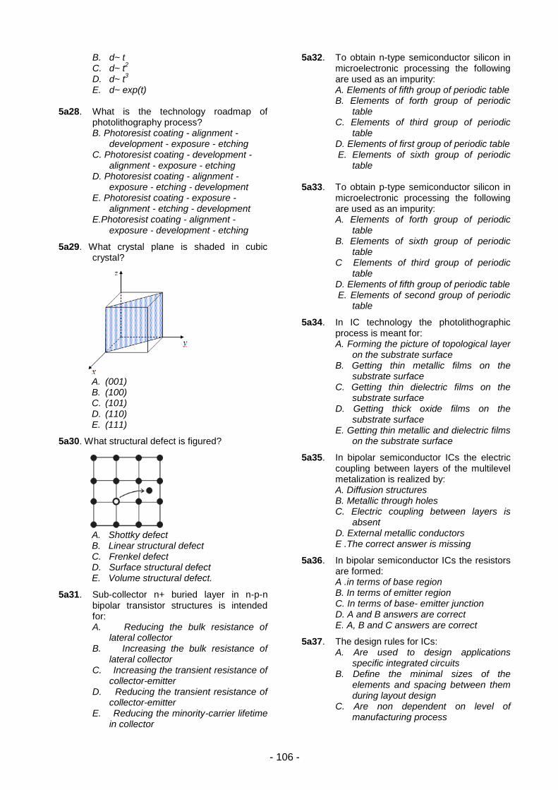
- 106 -
B. d~ t C. d~ t
2
D. d~ t3
E. d~ exp(t) 5a28. What is the technology roadmap of
photolithography process? B. Photoresist coating - alignment -
development - exposure - etching C. Photoresist coating - development -
alignment - exposure - etching D. Photoresist coating - alignment -
exposure - etching - development E. Photoresist coating - exposure -
alignment - etching - development E.Photoresist coating - alignment -
exposure - development - etching
5a29. What crystal plane is shaded in cubic crystal?
A. (001) B. (100) C. (101) D. (110) E. (111)
5a30. What structural defect is figured?
A. Shottky defect B. Linear structural defect C. Frenkel defect D. Surface structural defect E. Volume structural defect.
5a31. Sub-collector n+ buried layer in n-p-n bipolar transistor structures is intended for: A. Reducing the bulk resistance of
lateral collector B. Increasing the bulk resistance of
lateral collector C. Increasing the transient resistance of
collector-emitter D. Reducing the transient resistance of
collector-emitter E. Reducing the minority-carrier lifetime
in collector
5a32. To obtain n-type semiconductor silicon in microelectronic processing the following are used as an impurity: A. Elements of fifth group of periodic table B. Elements of forth group of periodic
table C. Elements of third group of periodic
table D. Elements of first group of periodic table E. Elements of sixth group of periodic
table
5a33. To obtain p-type semiconductor silicon in microelectronic processing the following are used as an impurity: A. Elements of forth group of periodic
table B. Elements of sixth group of periodic
table C Elements of third group of periodic
table D. Elements of fifth group of periodic table E. Elements of second group of periodic
table
5a34. In IC technology the photolithographic process is meant for: A. Forming the picture of topological layer
on the substrate surface B. Getting thin metallic films on the
substrate surface C. Getting thin dielectric films on the
substrate surface D. Getting thick oxide films on the
substrate surface E. Getting thin metallic and dielectric films
on the substrate surface
5a35. In bipolar semiconductor ICs the electric coupling between layers of the multilevel metalization is realized by: A. Diffusion structures B. Metallic through holes C. Electric coupling between layers is
absent D. External metallic conductors E .The correct answer is missing
5a36. In bipolar semiconductor ICs the resistors are formed: A .in terms of base region B. In terms of emitter region C. In terms of base- emitter junction D. A and B answers are correct E. A, B and C answers are correct
5a37. The design rules for ICs: A. Are used to design applications
specific integrated circuits B. Define the minimal sizes of the
elements and spacing between them during layout design
C. Are non dependent on level of manufacturing process

- 107 -
D. Are created by designer using design expertise
E. The correct answer is missing
5a38. In real p-n junctions beyond the defined value of the reverse voltage the reverse current: A. Sharply decreases B. Slowly decreases C. Sharply rises D. Slowly rises E. Remains practically constant
5a39. In semiconductor ICs to form the doped regions with required type and conductance in the substrate the following methods are used: A. Diffusion and ion implantation B. Ion implantation and thermal oxidation C. Ion etching and diffusion D. Diffusion and thermal oxidation E. The correct answer is missing
5a40. For the real p-n junction the main breakdown mechanisms are: A Thermal, tunnel and avalanche B. Tunnel, mechanical and thermal C. Thermal, radiation and chemical D. Avalanche, and electron-beam E. Thermal, electrochemical and tunnel
5a41. For a MOS structure transistor the minimal thickness of the oxide layer is limited by: A. Capabilities of the manufacturing
technology B. Values of the unwanted tunnel currents C. Critical electric field strength D. Defects concentration E. All the answers are correct
5a42. To compensate the radiation defects after the ion implantation doping the following processes are necessary: A. The additional doping with the donor
impurities B. The additional doping with the acceptor
impurities C. Thermal treatment in (600....800)
0C
range D. Thermal treatment in (1300....1500)
0C
range E. The mechanical planarization of the
crystal surface
5a43. In case of IC scaling by α >1 factor the power density changes in the following way: A. Decreases by α time B. Increases by α time C. Remains constant D. Increases by α
2 time
E. Decreases by α2 time
5a44. As a MOS-resistor forming region in MOS IC, the following are used:
A. Transistor’s channel B. Transistor’s source C. Transistor’s drain D. Gate’s insulator E. Metal gate
5a45. To reduce the resistivity of the polisilicon
in IC technology the following is
performed:
A. Impurities additional doping and silicide process
B. Ion etching and impurities additional doping
C. Silicide process and ion etching D. Surface oxidation and ion etching E. Silicide process and thermal oxidation
5a46. For an n-type silicon the donor impurity
concentration is Nd=1016
cm-3
. What kind
and which concentration of impurity will be
used to form p-n junction in this sample?
A. Boron with N > 1016
cm-3
B. Boron with N < 10
16 cm
-3
C. Boron with N = 1016
cm-3
D. Phosphorus with any concentration E. Phosphorus with N > 10
16 cm
-3
5a47. For a p-type silicon the acceptor impurity
concentration is Na =1015
cm -3
. What kind
and which concentration of impurity will be
used to form p-n junction in this sample?
A. Phosphorus with N = 1015
cm-3
B. Phosphorus with N < 1015
cm-3
C. Phosphorus with N >1015
cm-3
D. Boron with any concentration E. Boron with N > 10
15 cm
-3
5a48. The main limitations to reduce the feature
sizes of the nanoscale integrated circuits
are: A. Physical B. Technological C. Thermal D. Statistical E. All the answers are true
5a49. For contemporary integrated circuits the
signal time delay in the first place is
defined by: A. Gates time delay B. Interconnecting layers time delay C. Signals frequency range D. Structure of the package E. None of the above
5a50. The impurity maximum concentration in the
ion implanted layers is controlled by: A. Ion energy B. Ion angle of incidence C. Impurity doping dose

D. Doping temperature E. Thermal process temperature
5a51. As compared to the diffusion process, the
ion implantation is realized at: A. Higher temperatures B. Lower temperatures C. Same temperatures D. Presence of concentration gradient E. By neutral atoms flux
5a52. The basic manufacturing method to form
the layout pattern of contemporary
integrated circuits is: A. Ionic lithography B. Electron-beam lithography C. Subwavelength lithography D. Electromechanical lithography E. Molecular lithography
5a53. In VLSI technology the “dry” etching method
is realized by: A. Neutral atoms flux B. Accelerated ions flux C. Mechanical polishing D. Chemical-mechanical polishing E. Chemical solution
5a54. The basic requirement to the interlayer
dielectric material in the VLSI multilayer
interconnection structure is: A. High dielectric permittivity B. High specific conductivity C. High mechanical strength D. Low dielectric permittivity E. Dielectric layer is not used
5a55. What is mainly used in MOS integrated
circuits as a circuit resistor:
A. High doped source region B. High doped drain region C. Gate dielectric region D. Transistor channel region E. Resistive elements are not used
5a56. Design for manufacturability can be defined as: A. Checking all physical, electrical, and
logical errors, after the chip comes back from fabrication
B. Checking the chip before fabrication for operation at stress conditions such as low voltage, high temperature, and process variation
C. Checking the chip before fabrication for the correct functionality under nominal conditions
D. Designing techniques that allow the designer to test the chip after fabrication
E. None of the above
5a57. Signal propagation delay in IC, is mostly
determined by:
A. Delay of MOS transistors B. Delay of interconnects C. Structure of IC package D. The correct answer is missing E. The answers A,B and C are correct
5a58. To increase the gate specific capacitance
of a MOS transistor it is necessary to:
A. Use dielectric films with low permittivity
B. Decrease the thickness of dielectric film
C. Increase operation voltages D. Increase the area of the gate E. The correct answer is missing
5a59. To increase the gate specific capacitance
of a MOS transistor it is necessary to:
A. Increase the thickness of dielectric film
B. Use high permittivity (high-k) dielectric films
C. Decrease the area of the gate D. Increase operation voltages E. The correct answer is missing
5a60. The large-scale industry application of
electron beam lithography to produce IC
elements is limited by:
A. Extremely slow process B. Poor efficiency process C. Equipment complexity D. More expensive facilities E. All the answers are correct
5a61. In the current IC manufacturing process the
ion implantation is used to perform the
following technological operations:
A. Ion cleaning of the surface of semiconductor substrate
B. Ion etching of thin films and substrates
C. Adjusting transistor’s threshold voltage
D. Forming channel-stop layers E. All the answers are correct
5a62. The advanced technologies to form layout
pattern of ICs are:
A. Electron-beam lithography B. Immersion lithography C. Optical proximity correction (OPC)
technology D. Phase shift mask (PSM) technology E. All the answers are correct
- 109 -
5a63. In the IC manufacturing process the
chemical-mechanical-polishing (CMP)
technology is used:
A. To reduce the thickness of semiconductor substrate
B. For chemical activation of the substrate surface
C. For planarization of the substrate surface prior to lithography process
D. To form vias in the structure of multilevel metallization structure
E. All the answers are correct
5a64. The intrinsic silicon is doped simultaneously
with donor and acceptor impurities with the
concentrations Nd=1018
cm-3
and Na=1017
cm-3
respectively. What are the type of
conductivity and active concentration of
the silicon?
A. n-type, Nactive = 1017
cm-3
B. n-type, Nactive = 9x10
17 cm
-3
C. n-type, Nactive = 1018
cm-3
D. p- type, Nactive = 5x10
17 cm
-3
E. Intrinsic conductivity, Nactive = 0
b) Problems 5b1. For a silicon p-n junction the specific resistances of p and n-regions are 10
-4 Ohm
.m and 10
-2 Ohm
.m
correspondingly. Calculate the contact potential of the junction at a room temperature when T=300K if the mobility of holes and electrons are 0,05 m
2 V
-1 s
-1 and 0,13 m
2 V
-1 s
-1. The intrinsic concentration at a room
temperature equals 1,38x10¹⁶
m-3
.
5b2. Calculate the density of electrons and holes in a p-Ge at a room temperature if the sample specific conductance equals 100 S/cm, mobility of holes is 1900 cm
2 V
-1 s
-1, and ni=2,5x10
13 atom/cm
3.
5b3. The silicon sample is doped with a donor impurity Nd= 10
17atom/cm
3. The sample length equals 100μm,
width 10 μm, and thickness 1 μm. Calculate the resistance and sheet resistance.
5b4. What thickness of SiO2 layer is required to fabricate a MOS capacitor with a specific capacity of 100nF/cm
2 (ε
SiO2=3,8x8,85x10-14
F/cm). What oxidation process (wet or dry) would be used to grow the gate high quality oxide?
5b5.
The gate capacitance of the MOS transistor equals C. The capacitor structure is scaled by the factor =2 .
How will the gate capacitance change?
5b6. Semiconductor’s band gap width Eg = 0.7eV and the temperature does not change when T1 = 250 K changes
to T2 = 300 K. V=0.4V forward bias voltage is applied to the p-n junction created in it. Define 12 jj change of
current density in the mentioned range of temperature change if in case of T2 = 300 K, kT = 0.026eV.
5b7. How will the channel of a p-n junction field effect transistor change when the drain voltage is V=+0.1 V if the
dielectric transparency of semiconductor = 12, and for vacuum 0 = 8.8610-12
F/m, contact difference of
potentials k=0.6V, electron charge q=1.6*1019
K, and donor density in n channel Nd=1015
cm-3
. Ignore the effects of source-drain and gate-drain domains.
5b8. Calculate the drain current of a silicon n-MOSFET for the following conditions: Vt = 1 V, gate width W =
10 m, gate length L = 1m and oxide thickness tox = 10 nm. The device is biased with VGS = 3 V and VDS = 5 V. Use the device quadratic model, a surface mobility of 300 cm
2/V-s and VBS = 0 V.
5b9.
For a silicon n-channel MOS FET the source- drain distance is 1m and the doping levels are Nd =1020
cm
-3. The substrate doping is Na = 10
16 cm
-3. Assume that the source and substrate are grounded. At what VD
voltage on the drain the deplation widths of source and drain p-n junctions will meet (punch-through effect)?
5b10. The donor impurity concentration in the silicon substrate changes linearly N=kx [cm
-3 ], where k= 8 x 10
18
cm-4
and x is a distance. Calculate electrons diffusion current density when the electric field is absent.
Electrons mobility at room temperature (T=300 K) is 1200 cm2/Vs.
5b11. For a silicon n
+ - p - n bipolar transistor the base width is WB=0,6um, the doping levels of emitter, collector
and base are Nde =1019
cm-3
, Ndc =5x10¹⁶
cm-3
and Nab=5x10¹⁵
cm-3
respectively. Define the collector critical

- 110 -
voltage, when the device becomes uncontrolled (punch-through in the base region). Assume T=300 K and intrinsic concentration is ni=1,5x10
10 cm
-3.
5b12. The intrinsic silicon wafer is doped with donor Nd = 10
17 cm
-3 and acceptor Na =10
16 cm
-3 impurities
simultaneously. What is the silicon polarity of conductivity Calculate the specific conductivity of the sample
at room temperature T= 300 K. The electrons mobility at room temperature is 1400 cm2/Vs, and electron
charge is 1,6x10⁻¹⁹
C. 5b13. Estimate the time delay in a n
+ polysilicon interconnect for the following conditions: the line length
l=1mm, width b=1 m, the sheet resistance of polysilicon =200 /, and the specific capacity of the line
to the substrate C0=60 aF/m 2.
5b14. Estimate the time delay in the metal interconnect (metal 1) for the following conditions: the line length
l=1mm, width b=200 nm, the metal sheet resistance =0,1 /, and the specific capacity of the line to the
substrate C0=23 aF/m 2.
5b15. Consider a one-sided silicon p-n diode with Nd = 10
16 cm
-3 and Na = 10
18 cm
-3. Calculate the p-n junction
barrier layer capacitance for applied reverse voltages U1= 0 V and U2= -5 V. Assume the contact potential of
p–n junction at room temperature is 0,7 V, relative permittivity of silicon Si=11,8, dielectric constant 0=
8,85x10⁻¹⁴
F/cm and the junction area Sp-n = 10-5
cm2.
5b16. In the IC structure the polysilicon interconnect line is formed on the surface of the thick oxide layer and passed above the high doped n
+ region. Calculate the signal time delay for the conditions:
line length l= 50m, line width w=0,5m, sheet resistance =500/sq, oxide layer thickness tox=0,2m,
dielectric permittivity ox=3,9. 5b17. The MOS structure transistor is scaled by the factor. How will the transistor’s power consumption, power
density, time delay and switching energy change using the constant electric field scaling approach 5b18.
The semiconductor resistor is formed on the basis of MOS transistor’s n-well. The resistor’s length is 50 m
and width is 2,5m. Estimate the resistance change value over temperature range of 00C to 100
0C. The
sheet resistance of the n-well resistor at room temperature (270C ) is 300 /sq and temperature coefficient is
0,0024 1/ oC.
5b19. The diffusion resistor is formed in the emitter n
+ region of the bipolar transistor. The emitter layer thickness is
h=0,1 m and doping level is 1019
cm-3
. Calculate the resistance of the basic region for the conditions:
length l= 10 m, width w= 0,5 m, electron mobility n=1400 cm2/V s.
5b20. For a silicon semiconductor sample the donor impurity concentration Nd changes linearly from 10
18 cm
-3 to
5x10¹⁷
cm-3
, when the coordinate change is ΔX=3 mkm. Calculate the diffusion current density in the sample
when the electrical field is absent. The electrons mobility at room temperature is µ = 1200 cm2/Vs and the
thermal potential is t = 0,026 V.
5b21. The optical properties of photolithography system are described by the Rayleigh equations. Estimate the R resolution and F focus depth of the optical system. Accept that wavelength λ=193 nm, numerical aperture NA=0,65 and coefficients k1=0,3 and k2=0,5. Discuss the possibility to increase the resolution using the immersion lithography technology. 5b22. For a silicon n-channel MOS transistor the channel width is W = 5 mkm, channel length is L = 0,3 mkm, oxide thickness is tox = 15 nm and threshold voltage is Vt = 0,7 V. The device is biased with VGS = 1,5 V and VDS = 3 V. Calculate the drain current using the quadratic model. A surface mobility of electrons is 500
cm2/Vs and VBS = 0 V. Calculate the channel resistance for the same conditions.
5b23. Calculate the temperature when the resistance of the silicide polysilicon increases by 50% compared to room temperature (t=27
oC). The silicide polysilicon temperature coefficient of resistance is 0,0033 1/
oC.
- 111 -
6. NUMERICAL METHODS AND OPTIMIZATION
a) Test questions 6a1. Fragmentation consecutive algorithm,
compared with iteration algorithm, has: A. More accuracy B. Higher performance C. Less accuracy D. More machine time E. B and C together
6a2. Which is the inverse polynomial of X
4+X+1?
A. X3+X+1
B. X4+X+1
C. X4+X
2+1
D. X4+X
3+1
E. The correct answer is missing
6a3. Which of the given intrinsic description forms more accurately describes an electrical circuit? A. The graph of commutation schema B. Complex list C. Adjacency matrix D. A and B equally E. B and C equally
6a4. The following problem of linear programming:
:0x,0x
15x5x
42x6x7
maxx3x2
21
21
21
21
A. Does not have solution B. Has one solution C. Has two solutions D. Has solutions with infinite set E. Has unlimited solutions
6a5. In case of which values of parameter
the following problem has infinite set of solutions?
:0x,0x
,30x5x6
,2x4x
,2x2x
:D
,minxx)X(f
21
21
21
21
DX21λ
A. 2 B. 1/2 C. 1 D. 1/4 E. 1/8
6a6. In case of which values of 21,
parameters the following problem has one solution?
:0x,0x
,30x5x6
,2x4x
,2x2x
:D
,minxx)X(f
21
21
21
21
DX2211 λλ
A. 4,1 21 λλ
B. 1,2/1 21 λλ
C. 4,2 21 λλ
D. 8,4 21 λλ
E. 2,1 21 λλ
6a7. In case of what values of parameters
the following problem does not have a solution?
:0x,0x,0x,0xx2x
,2xx:D
,maxxxx)X(f
321
321
31
DX321
A. 0 B. 5 C. 1 D. 1/2 E. 2
6a8. In case of what values of 21b and 22b
elements
10
21
,
024
210
102
2221 bbBA
matrix system will not be fully controllable?
A. b210, b22=0 B. b21=0, b22=0
C. b210, b220
D. b21=0, b220 E. The correct answer is missing
6a9. In case of which values of 11b and 12b
elements
02
21,
420
012
201 1211 bb
BA
matrix system will not be fully controllable? A. b11=0, b12=0 B. b11=1, b12=2 C. b11=2, b12=0 D. b11=1, b12=0 E. b11=0, b12=1
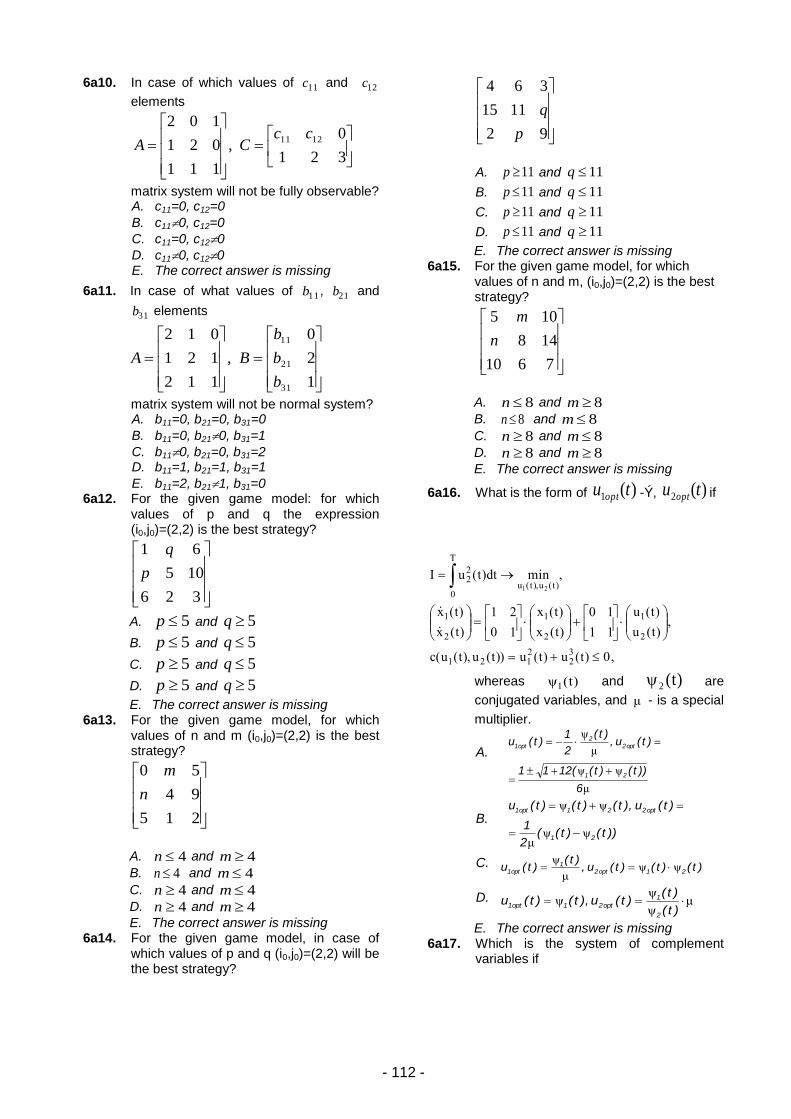
- 112 -
6a10. In case of which values of 11c and 12c
elements
321
0,
111
021
1021211 cc
CA
matrix system will not be fully observable? A. c11=0, c12=0
B. c110, c12=0
C. c11=0, c120
D. c110, c120 E. The correct answer is missing
6a11. In case of what values of 11b , 21b and
31b elements
1
2
0
,
112
121
012
31
21
11
b
b
b
BA
matrix system will not be normal system? A. b11=0, b21=0, b31=0
B. b11=0, b210, b31=1
C. b110, b21=0, b31=2 D. b11=1, b21=1, b31=1
E. b11=2, b211, b31=0 6a12. For the given game model: for which
values of p and q the expression (i0,j0)=(2,2) is the best strategy?
326
105
61
p
q
A. 5p and 5q
B. 5p and 5q
C. 5p and 5q
D. 5p and 5q
E. The correct answer is missing 6a13. For the given game model, for which
values of n and m (i0,j0)=(2,2) is the best strategy?
215
94
50
n
m
A. 4n and 4m
B. 4n and 4m
C. 4n and 4m
D. 4n and 4m
E. The correct answer is missing 6a14. For the given game model, in case of
which values of p and q (i0,j0)=(2,2) will be the best strategy?
92
1115
364
p
q
A. 11p and 11q
B. 11p and 11q
C. 11p and 11q
D. 11p and 11q
E. The correct answer is missing 6a15. For the given game model, for which
values of n and m, (i0,j0)=(2,2) is the best strategy?
7610
148
105
n
m
A. 8n and 8m
B. 8n and 8m
C. 8n and 8m
D. 8n and 8m
E. The correct answer is missing
6a16. What is the form of )(1 tu opt -Ý, )(2 tu opt if
,0)t(u)t(u))t(u),t(u(c
,)t(u
)t(u
11
10
)t(x
)t(x
10
21
)t(x
)t(x
,mindt)t(uI
32
2121
2
1
2
1
2
1
T
0)t(u),t(u
22
21
whereas )t(1ψ and )t(2 are
conjugated variables, and μ - is a special
multiplier.
A.
μ
ψψ
μ
ψ
6
))t()t((1211
)t(u,)t(
2
1)t(u
21
opt2
2
opt1
B. ))t()t((
2
1
)t(u),t()t()t(u
21
opt221opt1
ψψμ
ψψ
C. )t()t()t(u,)t(
)t(u 21opt2
1
opt1 ψψμ
ψ
D. μψ
ψψ
)t(
)t()t(u),t()t(u
2
1
opt21opt1
E. The correct answer is missing 6a17. Which is the system of complement
variables if
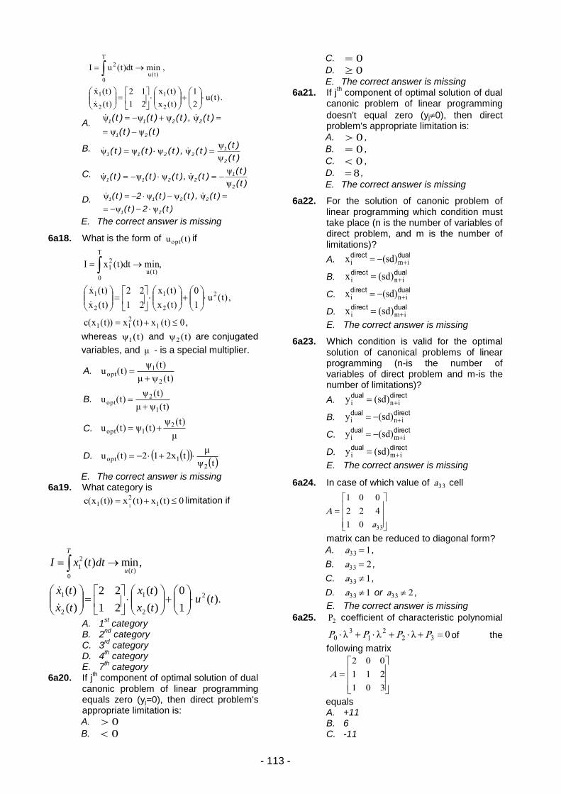
- 113 -
.)t(u2
1
)t(x
)t(x
21
12
)t(x
)t(x
,mindt)t(uI
2
1
2
1
T
0)t(u
2
A. )t()t(
)t(,)t()t()t(
21
2211
ψψ
ψψψψ
B. )t(
)t()t(,)t()t()t(
2
1
2211ψ
ψψψψψ
C. )t(
)t()t(,)t()t()t(
2
1
2211ψ
ψψψψψ
D. )t(2)t(
)t(,)t()t(2)t(
21
2211
ψψ
ψψψψ
E. The correct answer is missing
6a18. What is the form of )t(uopt if
,0)t(x)t(x))t(x(c
,)t(u1
0
)t(x
)t(x
21
22
)t(x
)t(x
,mindt)t(xI
1211
2
2
1
2
1
T
0)t(u
21
whereas )t(1ψ and )t(2ψ are conjugated
variables, and μ - is a special multiplier.
A. )t(
)t()t(u
2
1opt
ψμ
ψ
B. )t(
)t()t(u
1
2opt
ψμ
ψ
C. μ
ψψ
)t()t()t(u 2
1opt
D. t
tx212)t(u2
1optψ
μ
E. The correct answer is missing 6a19. What category is
0)t(x)t(x))t(x(c 12
1 1 limitation if
).(1
0
)(
)(
21
22
)(
)(
,min)(
2
2
1
2
1
0)(
2
1
tutx
tx
tx
tx
dttxI
T
tu
A. 1st category
B. 2nd
category C. 3
rd category
D. 4th category
E. 7th category
6a20. If jth component of optimal solution of dual
canonic problem of linear programming equals zero (yj=0), then direct problem's appropriate limitation is:
A. 0
B. 0
C. 0
D. 0
E. The correct answer is missing 6a21. If j
th component of optimal solution of dual
canonic problem of linear programming
doesn't equal zero (yj0), then direct problem's appropriate limitation is:
A. 0 ,
B. 0 ,
C. 0 ,
D. 8 ,
E. The correct answer is missing
6a22. For the solution of canonic problem of linear programming which condition must take place (n is the number of variables of direct problem, and m is the number of limitations)?
A. dualdirect
imi )sd(x
B. dualdirect
ini )sd(x
C. dualdirect
ini )sd(x
D. dualdirect
imi )sd(x
E. The correct answer is missing
6a23. Which condition is valid for the optimal solution of canonical problems of linear programming (n-is the number of variables of direct problem and m-is the number of limitations)?
A. directdual
ini )sd(y
B. directdual
ini )sd(y
C. directdual
imi )sd(y
D. directdual
imi )sd(y
E. The correct answer is missing
6a24. In case of which value of 33a cell
3301
422
001
a
A
matrix can be reduced to diagonal form?
A. 133 a ,
B. 233 a ,
C. 133 a ,
D. 133 a or 233 a ,
E. The correct answer is missing
6a25. 2P coefficient of characteristic polynomial
0322
13
0 PPPP λλλ of the
following matrix
301
211
002
A
equals A. +11 B. 6 C. -11
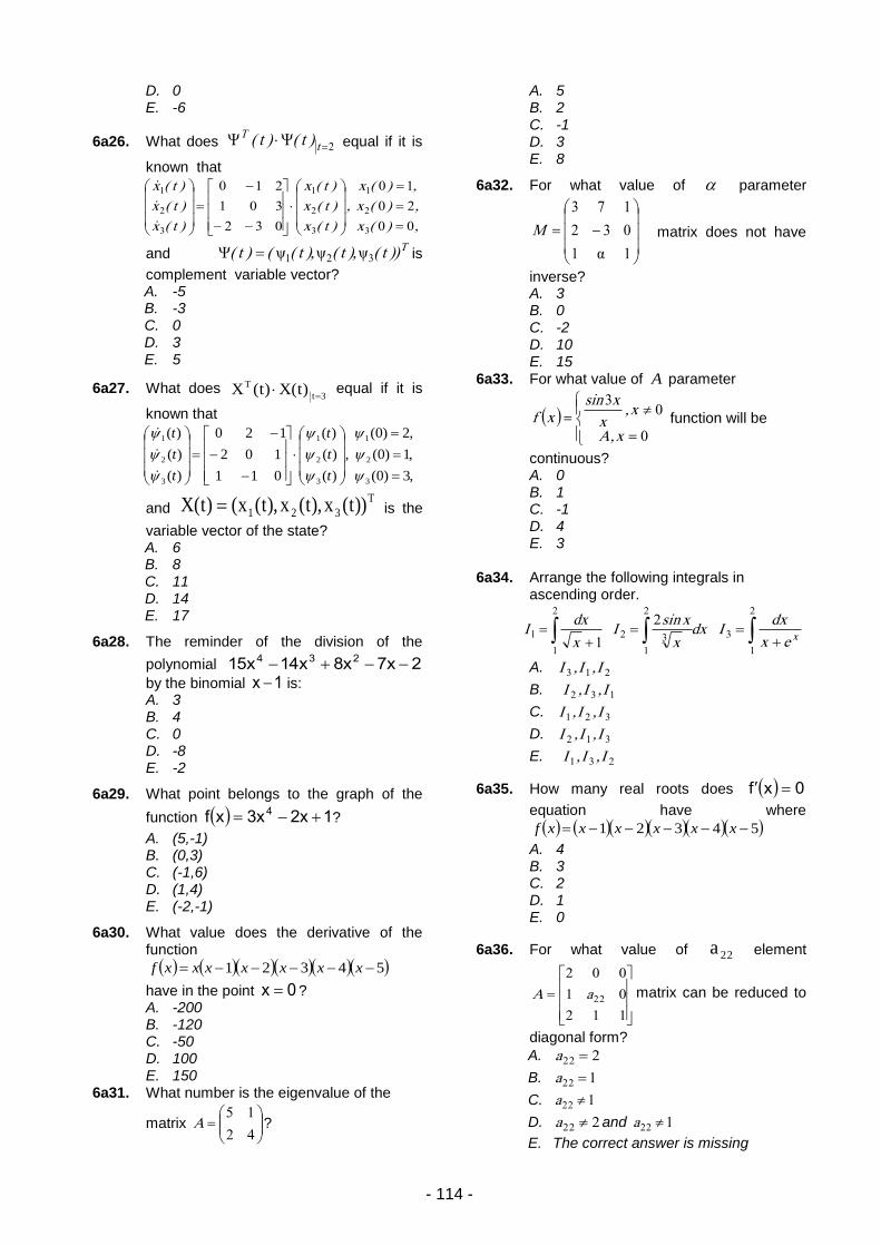
- 114 -
D. 0 E. -6
6a26. What does 2 tT )t()t( equal if it is
known that
,)(x
,)(x
,)(x
,
)t(x
)t(x
)t(x
)t(x
)t(x
)t(x
00
20
10
032
301
210
3
2
1
3
2
1
3
2
1
and T))t(),t(),t(()t( 321 ψψψ is
complement variable vector? A. -5 B. -3 C. 0 D. 3 E. 5
6a27. What does 3t
T )t(X)t(X
equal if it is
known that
,3)0(
,1)0(
,2)0(
,
)(
)(
)(
011
102
120
)(
)(
)(
3
2
1
3
2
1
3
2
1
t
t
t
t
t
t
and T
321 ))t(x),t(x),t(x()t(X is the
variable vector of the state? A. 6 B. 8 C. 11 D. 14 E. 17
6a28. The reminder of the division of the
polynomial 2x7x8x14x15 234
by the binomial 1x is: A. 3 B. 4 C. 0 D. -8 E. -2
6a29. What point belongs to the graph of the
function 1x2x3xf 4 ?
A. (5,-1) B. (0,3) C. (-1,6) D. (1,4) E. (-2,-1)
6a30. What value does the derivative of the function
54321 xxxxxxxf
have in the point 0x ? A. -200 B. -120 C. -50 D. 100 E. 150
6a31. What number is the eigenvalue of the
matrix
42
15A ?
A. 5 B. 2 C. -1 D. 3 E. 8
6a32. For what value of parameter
11
032
173
α
M matrix does not have
inverse? A. 3 B. 0 C. -2 D. 10 E. 15
6a33. For what value of A parameter
0
03
x,A
x,x
xsinxf function will be
continuous? A. 0 B. 1 C. -1 D. 4 E. 3
6a34. Arrange the following integrals in
ascending order.
2
1
11x
dxI dx
x
xsinI
2
1
32
2
2
1
3 xex
dxI
A. 213 I,I,I
B. 132 I,I,I
C. 321 I,I,I
D. 312 I,I,I
E. 231 I,I,I
6a35. How many real roots does 0xf
equation have where
54321 xxxxxxf
A. 4 B. 3 C. 2 D. 1 E. 0
6a36. For what value of 22a element
112
01
002
22aA matrix can be reduced to
diagonal form?
A. 222 a
B. 122 a
C. 122 a
D. 222 a and 122 a
E. The correct answer is missing
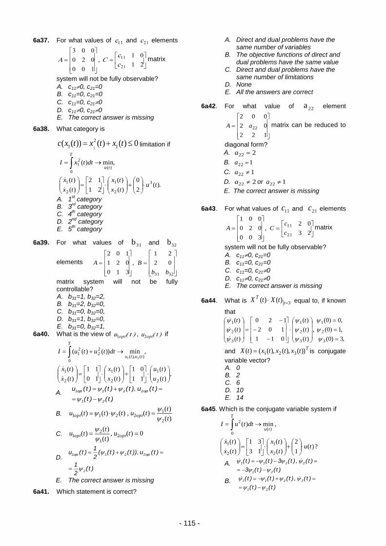
- 115 -
6a37. For what values of 11c and 21c elements
21
01
100
020
003
21
11
c
cC,A matrix
system will not be fully observable?
A. c110, c21=0 B. c11=0, c21=0
C. c11=0, c210
D. c110, c210 E. The correct answer is missing
6a38. What category is
0)()())(( 1
2
1 1 txtxtxc limitation if
).(2
0
)(
)(
21
12
)(
)(
,min)(
3
2
1
2
1
0)(
21
tutx
tx
tx
tx
dttxI
T
tu
A. 1st category
B. 3rd
category C. 4
th category
D. 2nd
category E. 5
th category
6a39. For what values of 31b and 32b
elements
3231
02
21
,
310
021
102
bb
BA
matrix system will not be fully controllable? A. b31=1, b32=2, B. b31=2, b32=0, C. b31=0, b32=0, D. b31=1, b32=0, E. b31=0, b32=1,
6a40. What is the view of )t(u opt1 , )t(u opt2 if
,)(
)(
11
01
)(
)(
10
11
)(
)(
,min))()((
2
1
2
1
2
1
0)(),(
22
21
21
tu
tu
tx
tx
tx
tx
dttutuI
T
tutu
A. )t()t(
)t(u),t()t()t(u
21
opt221opt1
B. )(
)()(,)()()(
2
12211
t
ttutttu optopt
C. 0)(,)(
)()( 2
1
21 tu
t
ttu optopt
D.
)t(2
1
)t(u)),t()t((2
1)t(u
2
opt221opt1
E. The correct answer is missing
6a41. Which statement is correct?
A. Direct and dual problems have the same number of variables
B. The objective functions of direct and dual problems have the same value
C. Direct and dual problems have the same number of limitations
D. None E. All the answers are correct
6a42. For what value of 22a element
122
02
002
22aA matrix can be reduced to
diagonal form?
A. 222 a
B. 122 a
C. 122 a
D. 222 a or 122 a
E. The correct answer is missing
6a43. For what values of 11c and 21c elements
23
02,
300
020
001
21
11
c
cCA matrix
system will not be fully observable?
A. c110, c21=0 B. c11=0, c21=0
C. c11=0, c210
D. c110, c210 E. The correct answer is missing
6a44. What is 3)()( tT tXtX equal to, if known
that
,3)0(
,1)0(
,0)0(
,
)(
)(
)(
011
102
120
)(
)(
)(
3
2
1
3
2
1
3
2
1
t
t
t
t
t
t
and TtxtxtxtX ))(),(),(()( 321 is conjugate
variable vector? A. 0 B. 2 C. 6 D. 10 E. 14
6a45. Which is the conjugate variable system if
?)(1
2
)(
)(
13
31
)(
)(
,min)(
2
1
2
1
0)(
2
tutx
tx
tx
tx
dttuI
T
tu
A. )t()t(3
)t(,)t(3)t()t(
21
2211
B. )t()t(
)t(,)t()t()t(
21
2211
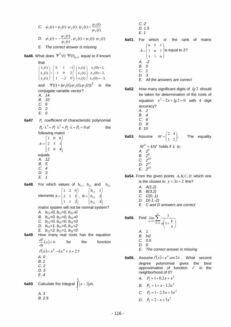
- 116 -
C. )(
)()(,)()()(
2
12211
t
ttttt
D. )()()(,)(
)()( 212
1
21 ttt
t
tt
E. The correct answer is missing
6a46. What does 2)()( tT tt equal to if known
that
,3)0(x
,2)0(x
,1)0(x
,
)t(x
)t(x
)t(x
021
201
110
)t(x
)t(x
)t(x
3
2
1
3
2
1
3
2
1
and Ttttt ))(),(),(()( 321 is the
conjugate variable vector? A. 14 B. 10 C. 6 D. 2 E. 0
6a47. 3P coefficient of characteristic polynomial
0322
13
0 PPPP λλλ of the
following matrix
402
132
001
A
equals A. 12 B. 5 C. 4 D. 3 E. 1
6a48. For which values of 11b , 21b and 31b
elements
3
2
1
,
211
112
021
31
21
11
b
b
b
BA
matrix system will not be normal system?
A. b110, b21=0, b310
B. b11=0, b21=0, b310 C. b11=0, b21=0, b31=0 D. b11=1, b21=0, b31=2 E. b11=2, b21=1, b31=0
6a49. How many real roots has the equation
0xdx
df for the function
26 46 xxxxf ?
A. 0 B. 1 C. 2 D. 3 E. 4
6a50. Calculate the integral .dxx
4
1
2
A. 3 B. 2.5
C. 2 D. 1.5 E. 1
6a51. For which the rank of matrix
α
α
α
11
11
11
A is equal to 2?
A. -2 B. 0 C. 1 D. 3 E. All the answers are correct
6a52. How many significant digits of 2lg should
be taken for determination of the roots of
equation 0222 lgxx with 4 digit
accuracy? A. 2 B. 4 C. 6 D. 8 E. 10
6a53. Assume
21
42M . The equality
kMM 6 holds if k is:
A. 26
B. 28
C. 210
D. 2
12
E. 214
6a54. From the given points DCBA ,,, which one
is the closest to 23 xy line?
A. A(1,2) B. B(3,2) C. C(0,-1) D. D(-1,-2) E. C and D answers are correct
6a55. Find
n
kn
n
kn
lim
1 1
1
A. 1 B. ln2 C. 0.5 D. 0 E. The correct answer is missing
6a56. Assume xcosexf x 2 . What second
degree polynomial gives the best approximation of function f in the neighborhood of 0?
A. 2
2 201 xx.P
B. 2
2 5.11 xxP
C. 2
2 3521 xx.P
D. 2
2 32 xxP
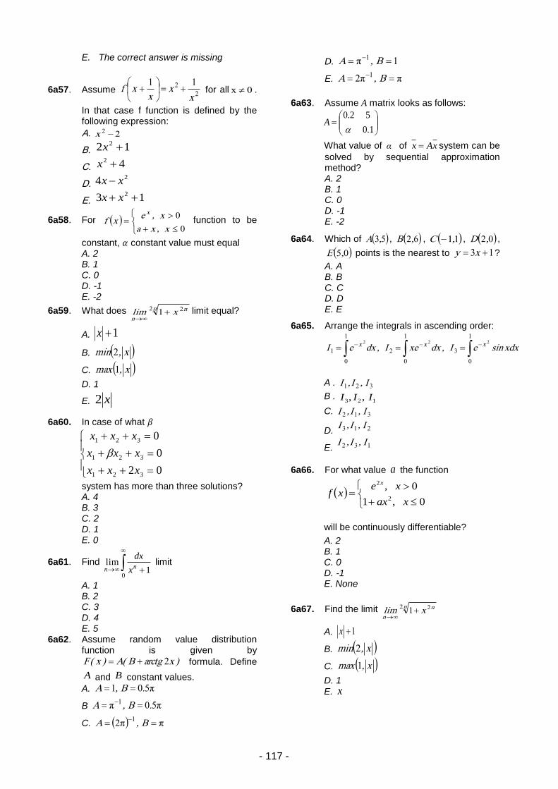
- 117 -
E. The correct answer is missing
6a57. Assume 2
2 11
xx
xxf
for all 0x .
In that case f function is defined by the following expression:
A. 22 x
B.
C.
D.
E.
6a58. For
0
0
x,xa
x,exf
x
function to be
constant, constant value must equal A. 2 B. 1 C. 0 D. -1 E. -2
6a59. What does n n
nxlim
2 21
limit equal?
A. 1x
B. x,min 2
C. x,max 1
D. 1
E. x2
6a60. In case of what
02
0
0
321
321
321
xxx
xxx
xxx
system has more than three solutions? A. 4 B. 3 C. 2 D. 1 E. 0
6a61. Find
0
1lim
nn x
dx limit
A. 1 B. 2 C. 3 D. 4 E. 5
6a62. Assume random value distribution function is given by
)xarctgB(A)x(F 2 formula. Define
A and B constant values.
A. π501 .B,A
B ππ 501 .B,A
C. ππ
B,A1
2
D. 11 B,A π
E. ππ B,A 12
6a63. Assume A matrix looks as follows:
1.0
52.0
A
What value of α of xAx system can be
solved by sequential approximation method? A. 2 B. 1 C. 0 D. -1 E. -2
6a64. Which of 53,A , 62,B , 11,C , 02,D ,
05,E points is the nearest to 13 xy ?
A. A B. B C. C D. D E. E
6a65. Arrange the integrals in ascending order:
1
0
3
1
0
2
1
0
1
222
xdxsineI,dxxeI,dxeI xxx
A . 321 I,I,I
B . 123 ,, III
C. 312 I,I,I
D. 213 I,I,I
E. 132 I,I,I
6a66. For what value a the function
0,1
0,2
2
xax
xexf
x
will be continuously differentiable?
A. 2 B. 1 C. 0 D. -1 E. None
6a67. Find the limit n n
nxlim
2 21
A. 1x
B. x,min 2
C. x,max 1
D. 1
E. x
12 2 x
42 x24 xx
13 2 xx
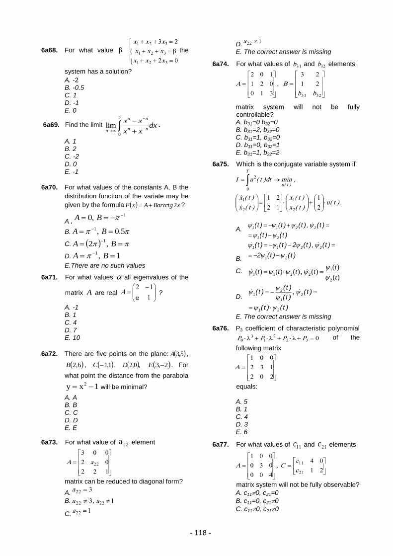
- 118 -
6a68. For what value β
02
23
321
321
321
xxx
xxx
xxx
β the
system has a solution?
A. -2 B. -0.5 C. 1 D. -1 E. 0
6a69. Find the limit dxxx
xxnn
nn
n
2
0
lim .
A. 1 B. 2 C. -2 D. 0 E. -1
6a70. For what values of the constants A, B the
distribution function of the variate may be
given by the formula xBarcctgAxF 2 ?
A .1,0 BA
B. 5.0,1 BA
C.
BA ,21
D. 1,1 BA
E.There are no such values
6a71. For what values all eigenvalues of the
matrix A are real
1
12
αA ?
A. -1 B. 1 C. 4 D. 7 E. 10
6a72. There are five points on the plane: 5,3A ,
6,2B , 1,1C , ,0,2D 2,3 E . For
what point the distance from the parabola
1xy 2 will be minimal?
A. A B. B C. C D. D E. E
6a73. For what value of 22a element
122
02
003
22aA
matrix can be reduced to diagonal form?
A.322 a
B. ,a 322 122 a
C.122 a
D.122 a
E. The correct answer is missing
6a74. For what values of 31b and 32b elements
3231
21
23
310
021
102
bb
B,A
matrix system will not be fully controllable? A. b31=0 b32=0 B. b31=2, b32=0 C. b31=1, b32=0 D. b31=0, b32=1 E. b31=1, b32=2
6a75. Which is the conjugate variable system if
.)t(u)t(x
)t(x
)t(x
)t(x
,mindt)t(uI
T
)t(u
2
1
12
21
2
1
2
1
0
2
A. )t()t(
)t(,)t()t()t(
21
2211
B. )t()t(2
)t(,)t(2)t()t(
21
2211
C. )(
)()(,)()()(
2
12211
t
ttttt
D.
)t()t(
)t(,)t(
)t()t(
21
2
1
21
E. The correct answer is missing
6a76. P3 coefficient of characteristic polynomial
0322
13
0 PPPP λλλ of the
following matrix
202
132
001
A
equals: A. 5 B. 1 C. 4 D. 3 E. 6
6a77. For what values of 11c and 21c elements
21
04
400
030
001
21
11
c
cC,A
matrix system will not be fully observable?
A. c110, c21=0
B. c11=0, c210
C. c110, c210
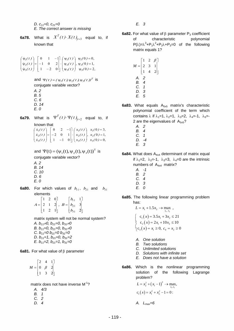
- 119 -
D. c11=0, c21=0 E. The correct answer is missing
6a78. What is 3 tT )t(X)t(X equal to, if
known that
,)(
,)(
,)(
,
)t(
)t(
)t(
)t(
)t(
)t(
20
10
00
021
201
110
3
2
1
3
2
1
3
2
1
ψ
ψ
ψ
ψ
ψ
ψ
ψ
ψ
ψ
and T))t(),t(),t(()t( 321 ψψψ is
conjugate variable vector?
A. 2 B. 5 C. 6 D. 14 E. 0
6a79. What is 2 tT )t()t( equal to, if
known that
,)(x
,)(x
,)(x
,
)t(x
)t(x
)t(x
)t(x
)t(x
)t(x
00
10
30
011
102
120
3
2
1
3
2
1
3
2
1
and T
321 ))t(),t(),t(()t( is
conjugate variable vector?
A. 2 B. 14 C. 10 D. 6 E. 0
6a80. For which values of 11b , 21b and 31b
elements
2
3
1
121
212
021
31
21
11
b
b
b
B,A
matrix system will not be normal system?
A. b110, b21=0, b310
B. b11=0, b21=0, b310 C. b11=0 b21=0 b31=0 D. b11=1, b21=0, b31=2 E. b11=2, b21=1, b31=0
6a81. For what value of parameter
2 4 1
0 2
1 3 2
M
matrix does not have inverse M-1
? A. 4/3 B. 1 C. 2 D. 4
E. 3
6a82. For what value of parameter P3 coefficient
of characteristic polynomial
P()=3+P1
2+P2+P3=0 of the following
matrix equals 1?
1 2
2 3 1
1 4 2
M
A. 2 B. 4 C. 1 D. 3 E. 5
6a83. What equals A5x5 matrix's characteristic
polynomial coefficient of the term which
contains if 1=1, 2=1, 3=2, 4=-1, 5=-
2 are the eigenvalues of A5x5? A. 2 B. 4 C. 1 D. -4 E. 3
6a84. What does A4x4 determinant of matrix equal
if 1=2, 2=-1, 3=3, 4=0 are the intrinsic
numbers of A4x4 matrix? A. -1 B. 2 C. 4 D. 3 E. 0
6a85. The following linear programming problem
has:
1 2
1 2,
1 1 2
2 1 2
3 1 4 2
1.5 max ,
c 3.5 3 21
c 2 10 10
c 0, 0
x xL x x
x x x
x x x
x x c x
A. One solution B. Two solutions C. Unlimited solutions D. Solutions with infinite set E. Does not have a solution
6a86. Which is the nonlinear programming
solution of the following Lagrange
problem?
1 2
22
2 1,
2 2
1 1 2
1 max,
1 0 :
x xL x x
c x x x
A. Lmax=6
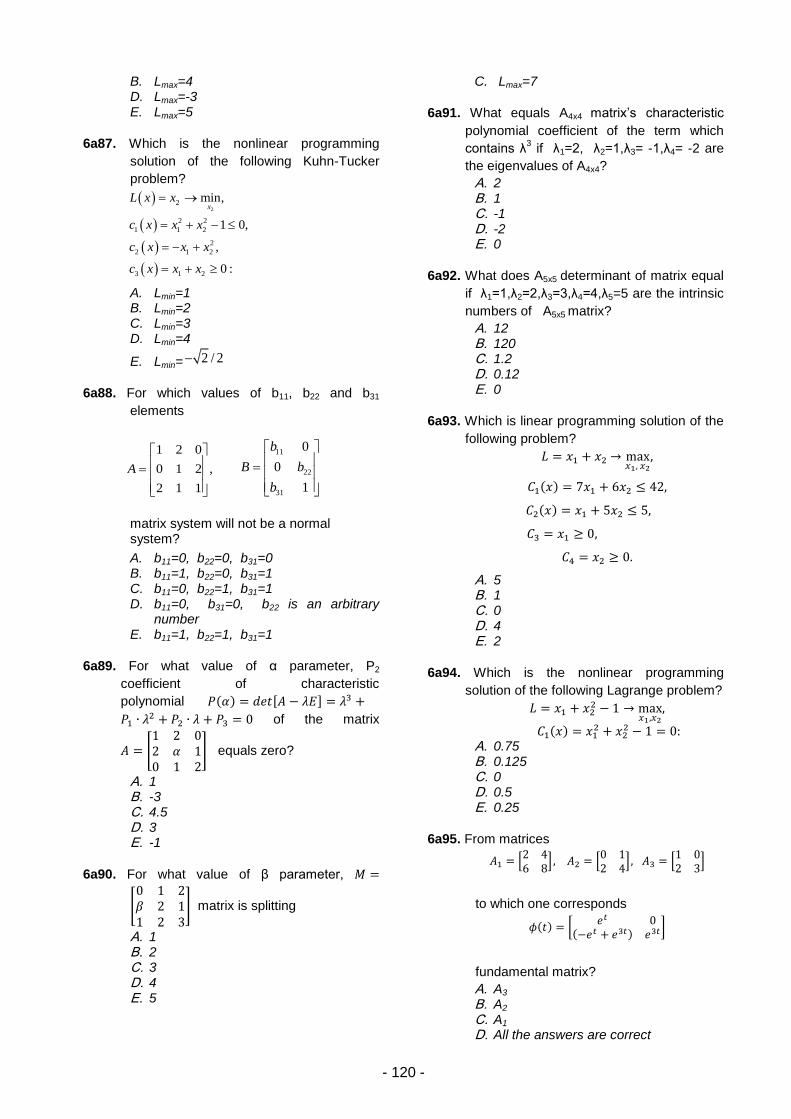
- 120 -
B. Lmax=4 C. Lmax=7 D. Lmax=-3 E. Lmax=5
6a87. Which is the nonlinear programming
solution of the following Kuhn-Tucker
problem?
2
2
2 2
1 1 2
2
2 1 2
3 1 2
min,
1 0,
,
0 :
xL x x
c x x x
c x x x
c x x x
A. Lmin=1 B. Lmin=2 C. Lmin=3 D. Lmin=4
E. Lmin= 2 / 2
6a88. For which values of b11, b22 and b31
elements
1 2 0
0 1 2 ,
2 1 1
A
11
22
31
0
0
1
b
B b
b
matrix system will not be a normal system?
A. b11=0, b22=0, b31=0 B. b11=1, b22=0, b31=1 C. b11=0, b22=1, b31=1 D. b11=0, b31=0, b22 is an arbitrary
number E. b11=1, b22=1, b31=1
6a89. For what value of α parameter, P2
coefficient of characteristic
polynomial ( ) [ ]
of the matrix
[
] equals zero?
A. 1 B. -3 C. 4.5 D. 3 E. -1
6a90. For what value of β parameter,
[
] matrix is splitting
A. 1 B. 2 C. 3 D. 4 E. 5
6a91. What equals A4x4 matrix’s characteristic
polynomial coefficient of the term which
contains λ3 if λ1=2, λ2=1,λ3= -1,λ4= -2 are
the eigenvalues of A4x4?
A. 2 B. 1 C. -1 D. -2 E. 0
6a92. What does A5x5 determinant of matrix equal
if λ1=1,λ2=2,λ3=3,λ4=4,λ5=5 are the intrinsic
numbers of A5x5 matrix?
A. 12 B. 120 C. 1.2 D. 0.12 E. 0
6a93. Which is linear programming solution of the
following problem?
( )
( )
A. 5 B. 1 C. 0 D. 4 E. 2
6a94. Which is the nonlinear programming
solution of the following Lagrange problem?
( )
A. 0.75 B. 0.125 C. 0 D. 0.5 E. 0.25
6a95. From matrices
[
] [
] [
]
to which one corresponds
( ) [
( ) ]
fundamental matrix?
A. A3 B. A2 C. A1 D. All the answers are correct
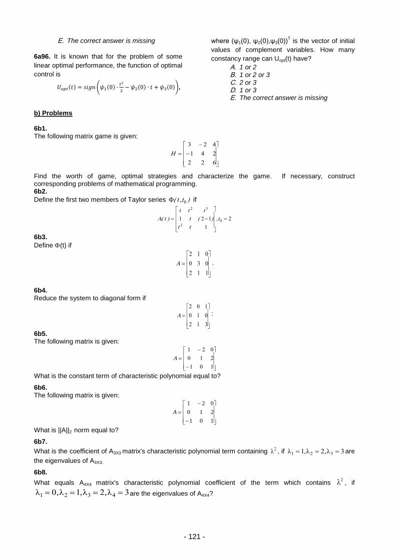
- 121 -
E. The correct answer is missing
6a96. It is known that for the problem of some
linear optimal performance, the function of optimal
control is
( ) ( ( )
( ) ( )),
where (ψ1(0), ψ2(0),ψ3(0))T is the vector of initial
values of complement variables. How many
constancy range can Uopt(t) have?
A. 1 or 2 B. 1 or 2 or 3 C. 2 or 3 D. 1 or 3 E. The correct answer is missing
b) Problems 6b1. The following matrix game is given:
622
241
423
H
Find the worth of game, optimal strategies and characterize the game. If necessary, construct corresponding problems of mathematical programming. 6b2.
Define the first two members of Taylor series )t,t( 0 if
2
1
121 0
2
32
t,
tt
)(t
ttt
)t(A
6b3.
Define (t) if
112
030
012
A .
6b4. Reduce the system to diagonal form if
312
010
102
A :
6b5. The following matrix is given:
101
210
021
A
What is the constant term of characteristic polynomial equal to?
6b6. The following matrix is given:
101
210
021
A
What is ||A||2 norm equal to?
6b7.
What is the coefficient of A3X3 matrix's characteristic polynomial term containing 2λ , if 321 321 λλλ ,, are
the eigenvalues of A3X3.
6b8.
What equals A4X4
matrix's characteristic polynomial coefficient of the term which contains 2 , if
3210 4321 λλλλ ,,, are the eigenvalues of A4X4?
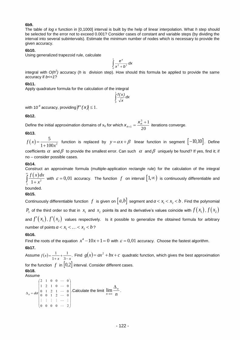
- 122 -
6b9. The table of log x function in [0,1000] interval is built by the help of linear interpolation. What h step should be selected for the error not to exceed 0.001? Consider cases of constant and variable steps (by dividing the interval into several subintervals). Estimate the minimum number of nodes which is necessary to provide the given accuracy.
6b10. Using generalized trapezoid rule, calculate
1
0
22dx
bx
e x
integral with O(h2) accuracy (h is division step). How should this formula be applied to provide the same
accuracy if b<<1?
6b11. Apply quadrature formula for the calculation of the integral
1
0
dxx
)x(f
with 10-4
accuracy, providing 1)x("f .
6b12.
Define the initial approximation domains of x0 for which20
13
1
nn
xx iterations converge.
6b13.
2
5
1 100f x
x
function is replaced by y x linear function in segment 10,10 . Define
coefficients and to provide the smallest error. Can such and uniquely be found? If yes, find it; if
no – consider possible cases.
6b14. Construct an approximate formula (multiple-application rectangle rule) for the calculation of the integral
2
11
f x dx
x
with 0,01 accuracy. The function f on interval 1, is continuously differentiable and
bounded.
6b15.
Continuously differentiable function f is given on ,a b segment and 1 2a x x b . Find the polynomial
3P of the third order so that in 1x and 2x points its and its derivative’s values coincide with 1f x , 2f x
and 1f x , 2f x values respectively. Is it possible to generalize the obtained formula for arbitrary
number of points 1 2a x x b ?
6b16.
Find the roots of the equation 4 10 1 0x x with 0,01 accuracy. Choose the fastest algorithm.
6b17.
Assume .3
1
1
1
xxxf
Find cbxaxxg 2
quadratic function, which gives the best approximation
for the function f in 2,0 interval. Consider different cases.
6b18. Assume
20
02
000
100
01
00
00
210
121
012
detn
.Calculate the limit n
n
n
lim .
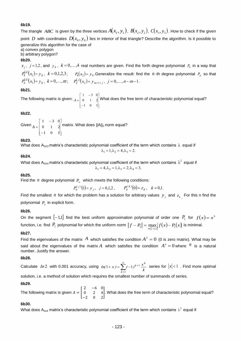
- 123 -
6b19.
The triangle ABC is given by the three vertices 11, yxA , 22 , yxB , 33 , yxC . How to check if the given
point D with coordinates 00 , yxD lies in interior of that triangle? Describe the algorithm. Is it possible to
generalize this algorithm for the case of a) convex polygon b) arbitrary polygon?
6b20.
jx , 21,j , and ky , 40 ,,k real numbers are given. Find the forth degree polynomial 4P in a way that
kk yxP 14 , 3210 ,,,k ; 424 yxP .Generalize the result: find the n -th degree polynomial nP so that
kk
n yxP 1 , m,,k 0 ; jmj
n yxP 12 , 10 mn,,j .
6b21.
The following matrix is given:
101
210
031
A What does the free term of characteristic polynomial equal?
6b22.
Given
101
210
031
Amatrix. What does ||A||2 norm equal?
6b23.
What does A3X3 matrix’s characteristic polynomial coefficient of the term which contains equal if
.,, 241 321 λλλ
6b24.
What does A4X4 matrix’s characteristic polynomial coefficient of the term which contains
2 equal if
.,,, 3214 4321 λλλλ
6b25.
Find the n degree polynomial nP which meets the following conditions:
2101 ,,j,yP j)j(
n , .,k,zP k)k(
n 100
Find the smallest n for which the problem has a solution for arbitrary values jy and kz
. For this n find the
polynomial nP in explicit form.
6b26.
On the segment 1,1 find the best uniform approximation polynomial of order one 1P for
3xxf
function, i.e. find 1P polynomial for which the uniform norm
xPxfPfx
11,1
1 max
is minimal.
6b27.
Find the eigenvalues of the matrix A which satisfies the condition 02 A (0 is zero matrix). What may be
said about the eigenvalues of the matrix A which satisfies the condition 0nA where n is a natural
number. Justify the answer.
6b28.
Calculate 2ln with 0.001 accuracy, using
1
111
k
kk
k
x)()xln( series for 1x . Find more optimal
solution, i.e. a method of solution which requires the smallest number of summands of series.
6b29.
The following matrix is given [
]. What does the free term of characteristic polynomial equal?
6b30.
What does A4x4 matrix’s characteristic polynomial coefficient of the term which contains 2λ equal if
- 124 -
:5.1,1,5.0,2 4321
6b31. Given the matrix of state variables of controlling system.
11
02A
Define )(t fundamental matrix of replacement.
6b32. Find out full controllability of the system described by the following equations.
,)t(u
)t(u
15.0
05.0
5.00
tx
tx
tx
5.05.00
05.05.0
105.0
tx
tx
tx
2
1
3
2
1
3
2
1
6b33. Estimate an accuracy of the rectangle’s symmetric rule
Iabba
fdxxfI
b
a
~
2
,
supposing that the function f two times continuously differentiable on the segment ba, .
6b34. Applying the rectangle’s symmetric rule
12
I~
abba
fdxxf
b
a
,
and the trapezoidal rule
22
I~
abbfaf
dxxf
b
a
,
to the integral
b
a
xdxeI
ln
ln
, where ba 0 , prove an inequalities
2
ba
alnbln
abab
(geometrical mean is less than logarithmical mean, which is less than arithmetical mean).
6b35.
A generalized Rolle’s theorem. Suppose the function f is continuous on b,a and 1n times continuously
differentiable on b,a . Let b,ax 0 be a point at which 0000 xfxfxf n . Then for arbitrary
point b,ax , 0xx at which 0xf there is a point 0, xx , such that 01 ηnf .
6b36.
Define the sequence of positive numbers: 00 x , n
nx
x
1
11 for 0n .
Prove that this sequence is converges and find the limit.
6b37.
Calculate the integral dxx
xsinI
.
50
0
with accuracy 0,001. That is, find number I such that 0010,II
.
6b38. The following matrix is given:
202
420
062
A
What does the free term of characteristic polynomial equal?
- 125 -
6b39.
What does A4x4 matrix’s characteristic polynomial coefficient of the term which contains 2λ equal if
.,,., 31502 4321 λλλλ
6b40. Given the matrix of state variables of controlling system.
22
01A
Define )(t fundamental matrix of replacement.
6b41. Find out full controllability of the system described by the following equations.
)t(u
)t(u
tx
tx
tx
tx
tx
tx
2
1
3
2
1
3
2
1
21
01
10
110
011
201
6b42. Given the matrix of state variables of controlling system.
31
01A
Define Φ(t) fundamental matrix of replacement
6b43. Find full controllability of system, described by the following motion equation.
11
1
2 2
2
33
1 0 1 1 0
0 1 1 :0 1
1 1 0 1 1
x tx t
u tx t x t
u tx t
x t
6b44. Find full observability of system, described by the following motion equation.
11
1
2 2
2
33
1 2 0 1 1
2 0 1 1 0
1 1 1 0 1
x tx t
u tx t x t
u tx t
x t
,
:
tx
tx
tx
t
t
3
2
1
2
1
123
021
6b45. What is the view of U1opt(t) and U2opt(t) if
1 2
2 2
1 2,
0
min ,
T
u t u tu t u t dt
1 1 1
2 22
1 1 1 0:
0 1 1 1
x t x t u t
x t u tx t
6b46. What does the sum of cubes of the roots of
[
]
matrix’s [ ] characteristic equation equal to?
6b47.
What does ( ) ( ) equal if it is known that
(
( )
( )
( )) [
] (
( )
( )
( ))
( )
( )
( )
- 126 -
and ( ) ( ( ) ( ) ( )) is conjugate variable vector.
6b48. Find the general forms of ( ) and ( ) if
∫ ( ( )
( )) ( ) ( )→
( ( )
( )) [
] ( ( )
( )) [
] ( ( )
( ))
- 127 -
7. DISCRETE MATHEMATICS AND THEORY OF COMBINATIONS
a) Test questions 7a1. The set is countable if it is
A. Finite B. Equivalent to some subset of finite set C. Equivalent to any subset of natural
number set D. Equivalent to any infinite set E. Equivalent to any infinite subset of
natural number set
7a2. The graph includes Euler cycle if and only if A. It is connected and the degrees of all
nodes are even B. It is connected and the degrees of
some nodes are odd C. The degrees of all nodes are even D. It is not connected and the degrees of
some nodes are even E. It is connected and the degrees of all
nodes are odd
7a3. If for )x,...,x,...,x(f ni1 Boolean function
f
i =1 (i=1,2,…,n), it is
A. Constant 1 function B. Linear function C. Self-dual function D. Monotone function E. Constant 0 function
7a4. If Boolean function is monotonous, then A. Its short disjunctive normal form does
not contain negation of variables B. It is not self-dual C. Its short disjunctive normal form does
not coincide with its minimal disjunctive normal form
D. it is also a threshold E. it is not a threshold
7a6. In the given design styles in what sequence does the performance increase in case of other same parameters a) library; b) gate matrix; c) full custom; d) programmable matrix; A. d - b - a - c B. a - b - c - d C. b - d - a - d D. c - a - b - d E. d - c - b - a
7a7. Which of the presented description forms of an electrical circuit is more convenient for the realization of sequential placing algorithm? A. Graph of commutation scheme B. Complex list C. Adjacency matrix D. A and B equally E. B and C equally
7a8. In case of the presented design styles, in what order does the density of cells’ placing increase? a) standard IC design; b) library design; c) gate matrix design; d) full custom design; e) programmable matrix design. A. b - a - c - e - d B. a - b - c - d - e C. d - c - b - e - a D. a - d - b - c - e E. d - b - c - e - a
7a9. The activity of 3x argument of
))()( 54321 xxvxxvx function equals
A. 1/4 B. 1/8 C. 3/8 D. 5/8 E. 3/4
7a10. If for f(x1, … , xn) Boolean function f
n,...,,21 =1, then f is
A. Constant 0 function B. Constant 1 function C. Monotone function D. Self-dual function E. Linear function
7a11. The activity of ))xxx(xx(x 654321
function’s 1x argument equals
A. 25/32 B. 27/32 C. 21/32 D. 13/16 E. 19/32
7a12. ))xxx(xx(x 654321
function’s norm
equals A. 11/64 B. 13/32 D. 17/64 D. 21/64 E. 23/64
7a13. ))()( 54321 xxvxxvx function’s norm
equals A. 7/16 B. 9/16 C. 13/16 D. 11/16 E. 5/16
7a14. f(x1, … , xn) is dual if
A. ),...,(f),...,( nn
αααα 11 =
),...,(f nαα1
- 128 -
B. ( ),...,(f),..., nn
αααα 11 =
),...,(f nαα1
C. ),...,(f),...,( nn
αααα 11 =
f (
),..., nαα1
D. ),...,( nαα1 ),...,(f n
αα1 =
),...,(f nαα1
E. ( ),...,(f),..., nn
αααα 11 =
),...,(f nαα1
7a15. The activity of the combination of
arguments 3x and 4x for the function
54321 x)xvx()xx( equals:
A. 1/4 B. 7/16 C. 3/4 D. 11/16 E. 1/8
7a16. If )x,...,x(f n1 is threshold function
A. )x,...,x(f n1
is not threshold function
B. )x,...,x(f n
1 is not threshold function
C. )x,...,x(f n
1 is threshold function
D. x )x,...,x(f n1 is threshold function
E. x )x,...,x(f n1
is threshold function
7a17. Binary relation is the equivalence relation if it is A. Transitive, symmetric but not reflexive B. Not symmetric, reflexive and transitive C. Symmetric, reflexive but not transitive D. Reflexive, transitive and symmetric E. Not symmetric, not reflexive and
transitive
7a18. ))xxvx()xvx( 54123 function’s norm
equals A. 9/16 B. 11/16 C. 13/16 D. 7/16 E. 5/16
7a19. The activity of ))xxvx()xvx( 54123
function’s 3x argument equals
A. 1/4 B. 1/8 C. 3/8 D. 5/8 E. 1/2
7a20. How many connectivity components does the complementation of the graph which has 4-connected component have?
A. 1 B. 2 C. 3 D. 4. E. The correct answer is missing
7a21. Given an n-input, m-output combinational circuit C, depending on input variables x1, x2, …, xn and output variables y1, y2, …, ym implementing functions fi(x1, x2, …, xn),
1im, and a combinational circuit C* implementing functions fj*(x1, x2, …, xn),
1jm, and obtained from C when a fault F (for example, single stuck-at-0 or stuck-at-1) occurs on its arbitrary line A. Set T of input vectors is a test with respect to
the set of faults if
A. For any f and for any an input
vector (1, 2, …, n) such that i
{0, 1},1in, and for any j, 1jm,
f*(1, 2, …, n) fj (1, 2, …, n);
B. For any f and for any input vector
(1, 2, …, n) such that i {0,
1},1in, and for any j, 1jm, fj*(1, 2, …, n) fj (1, 2, …, n);
C. For any f there exists an input
vector (1, 2, …, n) such that i
{0, 1},1in, and there exists a j,
1jm, such that fj*(1, 2, …, n) fj (1, 2, …, n);
D. For any f there exists such an input
vector (1, 2, …, n) such that i
{0, 1},1in, and there exists a j,
1jm, such that fj*(1, 2, …, n) fj (1, 2, …, n).
E. For any f there exists an input
vector (1, 2, …, n) such that i
{0, 1},1in, and there exists a j,
1jm, such that fj*(1, 2, …, n) fj (1, 2, …, n);
7a22. Given an n-input, m-output combinational circuit C, depending on input variables x1, x2, …, xn and output variables y1, y2, …, ym implementing functions fi(x1, x2, …, xn),
1im, and a combinational circuit C* implementing functions fj*(x1, x2, …, xn),
1jm, and obtained from C when a fault F (for example, single stuck-at-0 or stuck-
at-1) occurs on its arbitrary line A. Set (1, 2, …, n) detects fault F if
A. j, 1jm, and f*(1, 2, …, n) fj (1, 2, …, n);
B. for (1, 2, …, n) input patterns, i
{0, 1},1in, and for j, 1jm, fj*(1, 2, …, n) fj (1, 2, …, n);
- 129 -
C. for (1, 2, …, n) input patterns, for
i {0, 1},1in, and j, 1jm,
fj*(1, 2, …, n) fj (1, 2, …, n);
D. j, 1jm, so that fj*(1, 2, …, n) fj (1, 2, …, n);
E. j, 1jm, so that fj*(1, 2, …, n) fj (1, 2, …, n).
7a23. Given an n-input, m-output combinational circuit C, depending on input variables x1, x2, …, xn and output variables y1, y2, …, ym implementing functions fi(x1, x2, …, xn),
1im, and a combinational circuit C* implementing functions fj*(x1, x2, …, xn),
1jm, and obtained from C when a fault F (for example, single stuck-at-0 or stuck-at-1) occurs on its arbitrary line A. F fault cannot be detected with respect to some class faults if
A. (1, 2, …, n) such input pattern, i
{0, 1},1in, and j, 1jm, and
f*(1, 2, …, n) fj (1, 2, …, n);
B. 1. F fault cannot be detected or
2. G fault for which line B, for
which in case of (1, 2, …, n)
input pattern, i {0, 1},1in, and
j, 1jm, and f*(1, 2, …, n) = fj **(1, 2, …, n), where fj** is the function obtained from C when a fault G occurs on its line B
C. 1. fault F is detectable;
2.for (1, 2, …, n) input patterns,
for i {0, 1},1in, and j, 1jm,
fj*(1, 2, …, n) fj** (1, 2, …, n);
D. 1. fault F is detectable;
2. (1, 2, …, n) such input pattern,
i {0, 1},1in, and j, 1jm, so
that fj*(1, 2, …, n) fj **(1, 2, …,
n);
E. 1. fault F is detectable;
2. (1, 2, …, n) such input pattern,
i {0, 1},1in, and j, 1jm, so
that fj*(1, 2, …, n) fj **(1, 2, …,
n).
7a24. Given an n-input, m-output combinational circuit C, depending on input variables x1, x2, …, xn and output variables y1, y2, …, ym implementing functions fi(x1, x2, …, xn),
1im, and a combinational circuit C* implementing functions fj*(x1, x2, …, xn),
1jm, and obtained from C when a fault F (for example, single stuck-at-0 or stuck-at-1) occurs on its arbitrary line A. F fault is not redundant if
A. for (1, 2, …, n) input patterns, for i
{0, 1},1in, and j, 1jm, fj*(1, 2, …, n) fj (1, 2, …, n);
B. input pattern (1, 2, …, n) so that i
{0, 1},1in, and j, 1jm, for
which f*(1, 2, …, n) fj (1, 2, …,
n);
C. such input pattern (1, 2, …, n), i
{0, 1},1in, and j, 1jm, that
fj*(1, 2, …, n) = fj (1, 2, …, n);
D. such input pattern (1, 2, …, n), i
{0, 1},1in, and j, 1jm, so that
fj*(1, 2, …, n) fj (1, 2, …, n);
E. for input pattern (1, 2, …, n), i
{0, 1},1in, j, 1jm, so that fj*(1, 2, …, n) fj (1, 2, …, n).
7a25. Given an n-input, m-output combinational circuit C, depending on input variables x1, x2, …, xn and output variables y1, y2, …, ym implementing functions fi(x1, x2, …, xn),
1im, and a combinational circuit C* implementing functions fj*(x1, x2, …, xn),
1jm, and obtained from C when a fault F (for example, single stuck-at-0 or stuck-at-1) occurs on its arbitrary line A. Set T is
not a test with respect to set of faults if
A. f so that for (1, 2, …, n) input
patterns, for i {0, 1},1in, and j,
1jm, f*(1, 2, …, n) fj (1, 2, …,
n);
B. for f, for input pattern (1, 2,
…, n), for i {0, 1},1in, and j,
1jm, fj*(1, 2, …, n) fj (1, 2, …,
n);
C. for f, such input pattern (1, 2,
…, n), i {0, 1},1in, and j,
1jm, so that fj*(1, 2, …, n) fj (1, 2, …, n);
D. for f, such input pattern (1, 2,
…, n), i {0, 1},1in, and j,
1jm, so that fj*(1, 2, …, n) fj (1, 2, …, n).
F. E. f, for which, and for (1, 2,
…, n) input pattern, i {0, 1},1in,
and j, 1jm, fj*(1, 2, …, n) = fj (1, 2, …, n).
7a26. In a combinational circuit which has N lines, any number of stuck-at-0 or stuck-at-1 faults can occur. Find all possible multiple (not single) number of faults. A. 2
N
B. 3N
C. 3N - 1
D. 3N - 2
N - 1
E. 2N

- 130 -
7a27. What is a technical object model? B technical object is called A technical object model if through its experiments it is possible to have an idea about A technical object’s A. design B. properties C. parameters D. circuit E. structure
7a28. In what sequence are the following stages of digital IC design executed? a) layout design, b) behavioral-level design, c) logic design, d) RTL design A. c-a-b-d B. d-b-c-a C. b-d-c-a D. c-a-d-b E. a-b-c-d
7a29. In component level of IC design what kind of mathematical method is used? A. Probability theory B. Theory of queue system C. Boolean algebra D. Differential equations system E. Partial differential equations system
7a30. In case of the given elemental bases, in what sequence does the consumption power increase if the other parameters are similar? a) bipolar; b) CMOS; c) N-MOS A. b - c-a B. a-c-b C. a-b-c D. b-a-c E. c-b-a
7a31. Which of the given answers more contributes to the increase of performance in digital circuits? A. Decrease of load capacitance B. Increase of load capacitance C. Decrease of technological sizes D. Decrease of supply voltage E. A. and C. together
7a32. Which of the given answers more characterizes the advantage of a MOS elemental base in comparison to bipolar? A. Little consumption power B. High performance C. Simplicity of technology D. A and C together E. A and B together
7a33. A password must contain 2 numerals from the list {0, 1, 2, 3, 4, 5, 6, 7, 8, 9} and 4 letters from the list {a, A, b, B, c, C, d, D, e, E}. The first symbol must be a letter. Symbols may be repetitive. How many passwords can be generated meeting those conditions? A. 1 000 000
B. 2 000 000 C. 5 000 000 D. 8 000 000 E. 10 000 000
7a34. A password must contain 2 numerals from the list {0, 1, 2, 3, 4, 5, 6, 7, 8, 9} and 2 letters from the list {a, A, b, B, c, C, d, D, e, E}. The first symbol must be a letter. Symbols may be repetitive. How many passwords can be generated meeting those conditions? A. 100 000 B. 400 000 C. 600 000 D. 800 000 E. 1 000 000
7a35. A password must contain 2 numerals from the list {0, 1, 2, 3, 4, 5, 6, 7, 8, 9} and 3 letters from the list {a, A, b, B, c, C, d, D, e, E}. The first symbol must be a letter. Symbols may be repetitive. How many passwords can be generated meeting those conditions? A. 600 000 B. 800 000 C. 1 000 000 D. 1 200 000 E. 1 800 000
7a36. A password must contain 3 numerals from the list {0, 1, 2, 3, 4, 5, 6, 7, 8, 9} and 3 letters from the list {a, A, b, B, c, C, d, D, e, E}. The first symbol must be a letter. Symbols may be repetitive. How many passwords can be generated meeting those conditions? A. 100 000 B. 1 000 000 C. 10 000 000 D. 100 000 000 E. 1 000 000 000
7a37. 654321 xxxxxx norm of function
equals: A. 3/32 B. 9/32 C. 5/36 D. 7/32 E. 11/32
7a38. 654321 vxxxxxx norm of function
equals: A. 3/16 B. 1/8 C. 5/8 D. 1/16 E. 3/4
7a39. 654321 xxvxxvxx norm of function
equals: A. 21/32 B. 25/32 C. 27/32
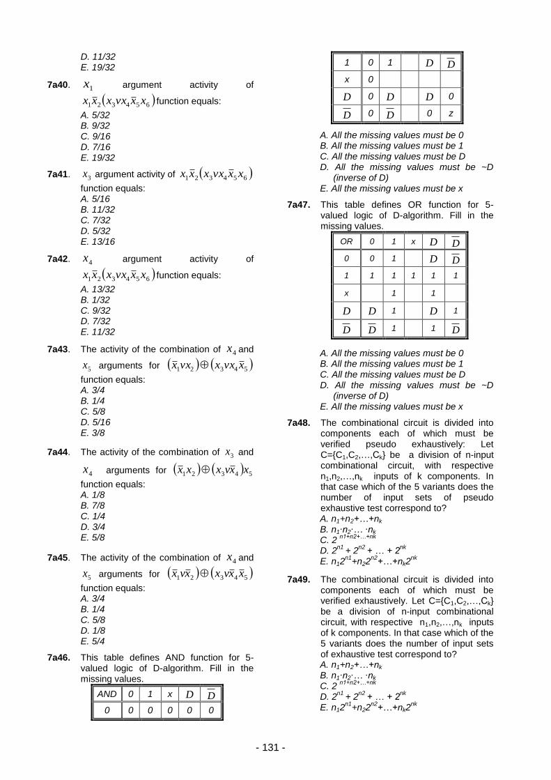
- 131 -
D. 11/32 E. 19/32
7a40. 1x argument activity of
654321 xxvxxxx function equals:
A. 5/32 B. 9/32 C. 9/16 D. 7/16 E. 19/32
7a41. 3x argument activity of 654321 xxvxxxx
function equals: A. 5/16 B. 11/32 C. 7/32 D. 5/32 E. 13/16
7a42. 4x argument activity of
654321 xxvxxxx function equals:
A. 13/32 B. 1/32 C. 9/32 D. 7/32 E. 11/32
7a43. The activity of the combination of 4x and
5x arguments for 54321 xvxxvxx
function equals: A. 3/4 B. 1/4 C. 5/8 D. 5/16 E. 3/8
7a44. The activity of the combination of 3x and
4x arguments for 54321 xxvxxx
function equals: A. 1/8 B. 7/8 C. 1/4 D. 3/4 E. 5/8
7a45. The activity of the combination of 4x and
5x arguments for 54321 xxvxxvx
function equals: A. 3/4 B. 1/4 C. 5/8 D. 1/8 E. 5/4
7a46. This table defines AND function for 5-valued logic of D-algorithm. Fill in the missing values.
AND 0 1 x D D
0 0 0 0 0 0
1 0 1 D D
x 0
D 0 D D 0
D 0 D 0 z
A. All the missing values must be 0 B. All the missing values must be 1 C. All the missing values must be D D. All the missing values must be ~D
(inverse of D) E. All the missing values must be x
7a47. This table defines OR function for 5-valued logic of D-algorithm. Fill in the missing values.
OR 0 1 x D D
0 0 1 D D
1 1 1 1 1 1
x 1 1
D D 1 D 1
D D 1 1 D
A. All the missing values must be 0 B. All the missing values must be 1 C. All the missing values must be D D. All the missing values must be ~D
(inverse of D) E. All the missing values must be x
7a48. The combinational circuit is divided into components each of which must be verified pseudo exhaustively: Let C={C1,C2,…,Ck} be a division of n-input combinational circuit, with respective n1,n2,…,nk inputs of k components. In that case which of the 5 variants does the number of input sets of pseudo exhaustive test correspond to? A. n1+n2+…+nk B. n1∙n2∙… ∙nk C. 2
n1+n2+…+nk
D. 2n1
+ 2n2
+ … + 2nk
E. n12
n1+n22
n2+…+nk2
nk
7a49. The combinational circuit is divided into components each of which must be verified exhaustively. Let C={C1,C2,…,Ck} be a division of n-input combinational circuit, with respective n1,n2,…,nk inputs of k components. In that case which of the 5 variants does the number of input sets of exhaustive test correspond to? A. n1+n2+…+nk B. n1∙n2∙… ∙nk C. 2
n1+n2+…+nk
D. 2n1
+ 2n2
+ … + 2nk
E. n12
n1+n22
n2+…+nk2
nk
- 132 -
7a50. 654321 xxvxxxx function’s
norm equals:
A. 9/16 B. 3/16 C. 5/16 D. 11/16 E. 1/16
7a51. 654321 xxvxxxx function’s norm equals:
A. 19/32 B. 17/32 C. 11/16 D. 19/32 E. 22/16
7a52. 654321 xxxvxxx function’s norm
equals:
A. 7/64 B. 21/32 C. 5/32 D. 13/16 E. 15/32
7a53. The activity of argument 1x for the
function 4321 vxxxx is equal to:
A. 5/8 B. 3/4 C. 1/4 D. 7/4 E. 5/4
7a54. The activity of argument 3x for the
function 4321 vxxxx is equal to:
A. 1/4 B. 1/2 C. 3/8 D. 5/8 E. 3/16
7a55. The activity of argument 5x for the
function 54321 xvxxxx is equal to:
A. 3/4 B. 5/8 C. 1/4 D. 3/8 E. 5/16
7a56. The activity of the combination of
arguments 4x and 5x for the function
54321 vxvxxxx is equal to:
A. 5/8 B. 3/2 C. 1/2 D. 5/2 E. 1/8
7a57. The activity of the combination of
arguments 1x and 2x for the function
54321 xvxvxvxx is equal to:
A. 5/8 B. 1/2 C. 3/4
D. 3/8 E. 5/16
7a58. The activity of the combination of
arguments 1x , 2x and 3x 2x for the
function 54321 xvxxxx is equal to:
A. 5/8 B. 3/16 C. 7/16 D. 5/16 E. 3/8
7a59. What design stage does the technological
mapping follow?
A. High level synthesis B. Logic synthesis C. Physical synthesis D. Circuit design E. Technological design
7a60. In what sequence do the effects of design
solutions increase on the final quality of
the design a) conceptual, b) structural and
c) parametrical synthesis steps?
A. a - b - c B. c - b - a C. b - c - a D. b - a - c E. c- a - b
7a61. What is the difference of electrical “short”
or “long” interconnects at most
characterized by?
A. Signal amplitude B. Signal power C. Signal edge increase D. Current power E. A. and B. together
7a62. Which of the numerated devices are used
in high level synthesis algorithms? a)
register; b) multiplexer; c) flip-flop; d)
transistor; e) inverter; f) driver
A. a-b-e B. a-c-f C. a-b-d-f D. a-b-f E. c-d-e-f
7a63. Let Q be the number of integers from the
segment [1,2, ... , 2010] that are divisible
by 2 and 3 but not by 5. Find the number
closest to Q.
A. 150 B. 200 C. 250 D. 300 E. 350
7a64. Let Q be the number of integers from the segment [1,2, ... , 2010] that are divisible by 3 and 5 but not by 7. Find the number closest to Q. A. 100 B. 120
- 133 -
C. 150 D. 170 E. 200
7a65. Let Q be the number of integers from the segment [1,2, ... , 2010] that are divisible by 3 and 7 but not by 11. Find the number closest to Q. A. 70 B. 80 C. 90 D. 100 E. 110
7a66. Let Q be the number of integers from the
segment [1,2, ... , 2010] that are divisible
by 5 and 7 but not by 11. Find the number
closest to Q.
A. 15 B. 20 C. 50 D. 70 E. 80
7a67. )xx(x321
norm of function equals A. 1/4 B. 1/2 C. 3/8 D. 3/4 E. 1/8
7a68.1
x argument activity of ))xx(x321
function equals A. 3/8 B. 19/32 C. 1/2 D. 1/8 E. 3/4
7a69.543
xxvx norm of function equals A. 1/4 B. 3/8 C. 3/4 D. 5/8 E. 1/2
7a70.3
x argument activity of 543
xxvx function
equals A. 1/4 B. 3/4 C. 5/8 D. 1/2 E. 3/8
7a71.1
x argument activity of
)xxvx()xvx(54321
function equals A. 3/4 B. 3/8
C. 1/2 D. 5/8 E. 7/16
7a72.The connected graph has ten vertices and six edges. How many new edges should be added to the graph to get a tree? A. 1 B. 2 C. 3 D. 4 E. 5
7a73.2
x argument activity of
54321x)xvx()xvx( function equals
A. 3/4 B. 5/8 C. 3/8 D. 7/16 E. 1/2
7a74. Given an n-input, 1-output combinational
circuit C, depending on input variables x1,
x2, …, xn and output variable y
implementing a function f(x1, x2, …, xn), and
a combinational circuit C* is given
implementing the function f*(x1, x2, …, xn)
obtained from C when a fault F (for
example, single stuck-at-0 or stuck-at-1)
occurs on its arbitrary line A. The fault F is
diagnosable with respect to a class of faults
if A. The fault F is necessarily detectable B. The fault F is not necessarily
detectable C. It is necessary and sufficient that the
fault F be detectable
D. All the faults from class are necessarily detectable
E. All the faults from class are not necessarily detectable
7a75. Given a 2-input, 1-output logic element of disjunction, depending on input variables x1, x2 and output variable Z implementing a function Z=x1+x2, and a combinational circuit C* is given implementing the function Z*(x1, x2) obtained from C when a fault F (for example, single stuck-at-0 or stuck-at-1) occurs on its input line A. The fault A/0 may be detectable by the help of the following set T of test patterns if
A. T={(00)} B. T={(11)} C. T={(10)} D. T={(00), (11)}
0 A
B Z*
Fault circuit
- 134 -
E. T={(00, (01), (11)}
7a76. Given a 2-input, 1-output combinational
circuit, depending on input variables a, b
and output variable f implementing a
function bb&af , and a combinational
circuit C* is given implementing the function
Z*(x1, x2) obtained from C when a fault F
(for example, single stuck-at-0 or stuck-at-
1) occurs on its input line A. “X” denotes the
fault A/0 (stuck-at-0). As a result of the fault
A/0, the circuit will implement a function f*:
A. bab&a*f
B. ba*f
C. ba*f
D. bb&a*f
E. b)ba(*f
7a77. Given a 2-input and 2-output sequential
circuit (flip-flop) depending on input
variables R, S and output functions Q, Q .
“X” denotes the fault A/0 (stuck-at 0).
Among the listed sequences of patterns
which one detects the fault A/0?
A. SR1=(01), SR2=(00) B. SR1=(11), SR2=(11), …, SR11=(11) C. SR1=(00),SR2=(01),SR3=(10),
SR4=(11) D. SR1=(11),SR2=(00),SR3=(10),
SR4=(01) E. SR1=(11), SR2=(00)
7a78. Which of elements are used in high level
synthesis algorithms: a-Boolean logic
elements; b- multiplexer; c-FF; d-transistor;
e-register; f-driver? A. c -d-e-f B. a-c-f C. a-b-e D. a-b-d-f E. b -e-f
7a79. How is the operation of a selector
organized? A. “False signal” is given to horizontal
input and basic input B. “False signal” is given to horizontal
input and “true signal” to basic input C. “True signal” is given to horizontal
input and basic input D. “True signal” is given to horizontal
input and “false signal” to basic input E. None of the above
7a80. Parametrical synthesis of a circuit precedes
the design phase of: A. Logic design B. Structural synthesis of a circuit C. Layout D. High level synthesis E. None of the above
7a81. For synchronization of Data Flow Graph
(DFG) it is necessary to insert in graph:
A. Registers B. Selectors C. Inverters D. Buffers E. None of the above
7a82. The design consists of 30 transistors of
different widths. Two groups by 15 and 8
transistors from this design are chosen. In
how many ways can this selection be made
such that the width of arbitrary transistor
from the first group will be less than width of
arbitrary transistor from the second group? A. 23
30A
B. 2330
C. 23
30C
D. 3023
E. 15
38A
7a83. For what values of a and b the straight line
y=ax+b and circle (x-1)2+(y-1)
2≤1 intersect?
A. 0b,1a
B. 1b,0a
C. 1b,2a
D. 2b,1a
E. 1b,1a
7a84. For what value of α the system of linear
equations has more than two solutions?
1
12
4
321
321
321
xxx
xxx
xxx
A. 1 B. 0
a
b f
R
S
Q
Q
’
line A
stuck-at-0

C. 1 D. 2 E. 3
7a85. For what value of α the function f(x)=αx3 -
3x2 + 3αx - 1 increases on all real line?
A. -1 B. -0.5 C. 0 D. 0.5 E. 1
7a86.The graph of the function nx
nx
n e1
xelimxf
is the function A. xx5.0
B. xx5.0
C. xx2
D. xx
E. x2
7a87. Calculate the integral dxxxI
4
0
3sgn .
Here
0,0
0,sgn
x
xx
x
x .
A. -2 B. -1 C. 0 D. 1 E. 2
7a88. From the 6 letters of the alphabet the word
“Ararat” is composed. A child, who does not
know how to read, mixed those letters and
then assembled them in a random order.
Find the probability that the new word will
also be “Ararat”.
A. 10
1
B. 30
1
C. 60
1
D. 180
1
E. 540
1
7a89. Let’s denote as signal the sequence of the
eight symbols such that each of them is one
of the letters A, B, C, D. How many signals
can be composed? A. 84
B. 4
8C
C. 4
8A
D. 48
E. 4
12C
7a90. Given is the following numerical integration
formula (Adam-Bashford):
)υ(x Δt24
91)υ(x Δt
24
37
2)υ(x Δt24
593)υ(x Δt
24
553)υx(4)υx(
Which of the following properties does this method have?
A. Implicit B. Explicit C. Three-step method D. Four-step method E. B and D variants are correct
7a91. Controllability and observability are defined
as: A. The ability to control the chip from the
input pins only B. The ability to test the whole chip easily
through checking the signals at output pins
C. Two metric used in chip-testing to measure testability
D. Two metric used before chip fabrication to test the level of manufacturability
E. None of the above
7a92. Which one of the listed tests for memory
devices is a March test?
A. {⇕ (w0); (r0, w1); (r1, w0) }
B. {⇕ (w0); (r1, w0); (r1, w0) }
C. {⇕ (w0); (r1, w0); (w0, r0)}
D. {⇕ (w0); (r0, w1); (r1, w0) }
E. {⇕ (w0); (r0, w1); (r0, w0) }
7a93. What is the complexity of a March test?
A. Linear B. Square C. Cubical D. Exponential E. NP-hard
7a94. What is the complexity of the traditional
GALPAT test?
A. Linear B. Square C. Cubical D. Exponential E. NP-hard
7a95. What is the complexity of D-algorithm?
A. Linear B. Square C. Cubical

- 136 -
D. Exponential E. Constant
7a96. In oriented graph, what is called a set of
strongly connected components?
A. The set of components which all are connected to one another by sides
B. The set of components where from any component there is a path to all the other components
C. The set of components which has at least one vertex from where there are paths to all the other components
D. The set of components which lacks cycles
E. The correct answer is missing
7a97. What do micromodels characterize?
A. Separate micromodules B. Information processes, occurring in the
object that is being designed C. Separate elements D. Interrelations, present between
elements E. Physical processes, occurring in solid
environment
7a98. What logic-geometrical operation is
presented?
A. OR B. AND C. XOR D. NOT E. NOR
7a99. In the square with the unit length side the
triangle is inscribed (all vertices are on the
sides of the square). What is the maximal
area of such triangle?
A.
1
3
B.
1
2
C.
2
3
D.
3
4
E.
5
6
7a100. Calculate the integral `
3
2
1
1x dx
A. 10 B. 2 C. 4 D. 6 E. 8
7a101. For what values of a and b the function
2 1,
,
3
3
x xf x
ax b x
is continuously
differentiable?
A. a=6, b= -8 B. a=8, b= -6 C. a=6, b=8, D. a= -6, b= -8, E. a=1, b=0
7a102. The straight lines 1y x , 10y x ,
6y and the points A(2.5; 5), B(3.5;
5), C(4.5; 5), D(5.5; 5), E(6.5; 5) are
given. Which point is inside the triangle
formed by those straight lines?
A. A B. B C. C D. D E. E
7a103. For what the function
2 3 22 1f x x x x increases
on the real line?
A. -1 B. 0 C. 1 D. 2 E. -2
7a104. Sort the integrals in the ascending order.
5.0
5.0
2
3
5.0
5.0
2
2
5.0
5.0
3
1sin,cos,sin xdxxIxdxxIxdxxI
A. I1, I2, I3 B. I3, I2, I1 C. I2, I1, I3 D. I3, I1, I2 E. I2, I3, I1
A
B
- 137 -
b) Problems 7b1.
Construct Zhegalkin polynomial for the threshold function with threshold w=3 and weights of variables 1=2,
2=2, 3=2.
7b2.
Verify the completeness of functions’ { 21 xx , 21 xx , 321 xxx } system.
7b3.
Using Post theorem verify the completeness of functions’ { x,0,1 , 321 xxx } system.
7b4.
Construct Zhegalkin polynomial of 3
21
xxx function.
7b5. Prove that for N bit number it is possible to calculate the number of 1-s for O(logN) time.
7b6. Prove that in N bit number it is possible to calculate the number of 1s in O(M) time where M is the number of 1s.
7b7. Prove that in unordered array K
th search can be executed in linear time.
7b8. Prove that ordering based on binary heap is executed in O(NlogN) time.
7b9. Construct complete disjunctive normal form of the Boolean function given by 11011011 table.
7b10. Construct Zhegalkin polynomial of the Boolean function given by 11011101 table.
7b11. Cayley code of G tree by numbered nodes is given h(G)=(3,5,4,4,5,6,7,8). Reconstruct the tree.
7b12.
Check the completeness of { 212121 ,,32 xxxxvxxxx
} system of functions.
7b13. Cayley code of G tree by numbered nodes is given h(G)=(3,2,4,4,5,6,8,8). Reconstruct the tree.
7b14.
Check the completeness of { 212121 ,,13 xxxxvxxxx
} system of functions.
7b15.
Calculate arguments’ 10,7,5,2 4321 balances and argument activities having w=10
threshold function.
7b16.
Check the completeness of functions’ { 21212121 ,,, vxxxxxxxx } system.
7b17.
Given an n-input Boolean function f(x1, x2, …, xn) = x1 x2 … xn. Construct the Binary Decision Diagram for f(x1,…, xi,…, xn). 7b18. Figure depicts the circuit of an n-bit adder. Prove that all possible single stuck-at-0 and stuck-at-1 faults on all lines of that circuit can be detected by means of only 8 test vectors.
- 138 -
7b19. Figure depicts the circuit of an N-input parity tree. Prove that all possible single stuck-at-0 and stuck-at-1 faults on all lines in that circuit can be detected by means of only 4 test vectors.
7b20. Figure depicts the circuit of N-input tree with negated Modulo 2 elements (gates XOR). Prove that all possible single stuck-at-0 and stuck-at-1 faults on all lines of that circuit can be detected by means of only 4 test vectors.
7b21. The given combinational circuit has 1000000 lines. Constant 0 or constant 1 faults of random numbers can occur there. Find the number of all possible multiple faults.
7b22. Given a Linear Feedback Shift Register corresponding to characteristic polynomial 1+x+x
3. Find the subsets
of all patterns which are generated by the given LFSR.
7b23. Given a Linear Feedback Shift Register corresponding to characteristic polynomial 1+x+x
3. Transform the
circuit, adding elementary cell(s) in a way that the obtained new circuit generates one set, consisting of all patterns.
S1
C1
a1 c1 b1
…
a2 c2 b2 an cn bn
S2 Sn
C2 Cn
x0
x1 x2
x0
x1 x2
- 139 -
7b24.
Construct Zhegalkin polynomial of the Boolean function given by21
31
xxxxf
.
7b25. By root tree’s 000101001111 code, reconstruct that tree.
7b26.
Calculate arguments activities of )( 32121 xxxxx function.
7b27. Cayley code of G tree by numbered nodes is given h(G)=(2, 3, 3, 4, 5, 5, 8) Reconstruct the tree.
7b28. Let T(F) be a test set for a fault F, a set of all possible input patterns detecting F.
Definition: Faults F1 and F2 from T(F) are called equivalent faults if T(F1) T(F2) and T(F2) T(F1), i.e., T(F1) = T(F2).
Find the faults that are equivalent to the mentioned in the figure fault “line A stuck-at-1”.
7b29. The combinational circuit is partitioned into components each to be tested exhaustively. Let C={C1,C2,…,C5} be a partition of a combinational circuit with n inputs into 5 components with 12, 14, 16, 18, 20 primary inputs. Calculate the number of input patterns for the pseudoexhaustive test with respect to the partition.
7b30. Let T(F) be a test set for a fault F, a set of all possible input patterns detecting F.
Definition: Faults F1 and F2 from T(F) are called equivalent faults if T(F1) T(F2) and T(F2) T(F1), i.e., T(F1) = T(F2).
Prove that faults F1, F2 and F3 are equivalent.
7b31. Suppose, given a 2-input, 1-output combinational circuit depending on input variables A, B and Z output variable implementing the function of conjunction Z=A B. Let T(F) be a test set for a single fault F, a set of
all possible input patterns detecting F.
Definition: Faults F1 and F2 from T(F) are called equivalent faults if T(F1) T(F2) and T(F2) T(F1), i.e., T(F1) = T(F2).
Prove that faults F1, F2 and F3 are equivalent.
7b32. In the given directed graph, realize search according to depth starting from the 2
nd vertex.
A
B
Z*
1
A
B
Z
F1: B S-a-1
F2: A S-a-1
F3: ZS-a-1
F1
F2
F3 A
B
Z
3 2 4 1
5 6 7 8

- 140 -
7b33. In the given directed graph, separate strongly connected components.
7b34. For the given directed graph, perform topological sorting.
7b35. In 7 x 7 discrete field realize Lee algorithm by the following initial conditions: The connecting contact coordinates A(1;2) , B(7;5). Objective functions are: f1 – number of crossings; f2 – connection length. Both objective functions are minimizing and respectively have the following importance coefficients a1=2, a2 =1. The discrete values of already occupied interconnections are: (2,5); (3,5); (4,1); (4,2); (4,3); (4,4); (4,5); (6,1); (6,3); (6,4); (6,5); (6,6) 7b36. Given net’s contact coordinates, having 5 contacts in a discrete field in conditional units: a(2,9); b(8,8); c(2,5); d(8,3); e(2,2): It is required to construct the orthogonal distance matrix of contacts and by its help compute the minimal tree by Prim’s algorithm, realizing the given net. 7b37. For the given graph construct adjacency matrix and using partitioning sequential algorithm, partition into 2 equal parts. As an optimality criterion, take the minimum of connection numbers between the parts.
7b38. Perform initial placement of the given circuit on the line using adjacency matrix, and using minimum interconnects length condition. As an initial element, take e1 cell.
7b39. Construct the timing graph of the given circuit and compute its critical path delays if the cell delays are given
3 2 4 1
5 6 7 8
1 2 3 4
5 6 7 8
2 3 3
3 3
2 3 3 3
3 3
2 1 3 3
3 3
2
4 3 3
3 3
2
5 3 3
3 3
2
6 3 3
3 3
2
e1
e4 e2
e3
e5
- 141 -
in conditional units: C1=C3=5, C2=10, C5=20, C4=C6=C7= 30.
7b40.
Construct Zhegalkin polynomial of 31
21
xxxxf
Boolean function.
7b41. Reconstruct the tree of root tree by 001010001111 code.
7b42.
Calculate argument activities of )( 2131 xxxx function.
7b43.
),,( 321 xxxf threshold function’s variable weights are: ξ1=3, ξ2=4, ξ3=6, and the threshold w=5.
Construct the perfect disjunctive normal form of ),,( 321 xxxf function.
7b44.
Check the completeness of ),, 213121 xxxxxx system of functions.
7b45. Construct Zhegalkin polynomial of the Boolean function given by last column of truth table - 11001011.
7b46.
Calculate arguments activities of )xxvx()xvx(43121
function.
7b47.
Check the completeness of {2121
x
2
x
1xx,xx,xx 13 } system of functions.
7b48.
)x,x,x(f321
threshold function’s variable weights are: ,4,3,2321 and threshold .4w Calculate
arguments activities of the function.
7b49. Construct Zhegalkin polynomial for the threshold function with threshold w=8 and weights of variables
5,4,3,24321 .
7b50. By root tree’s 000100011111 code, reconstruct that tree.
7b51. Given a combinational circuit with 3 inputs and 1 output depending on input variables x1, x2, x3 and output variable f realizing the function f=x1x2+x3. By using the method of Boolean differences, find all test patterns detecting the fault “line g stuck at 0” (g/0).
X1
X2
g
f
X3
1
5
8
2 3
4
6
7 9
10
- 142 -
7b52. Given a combinational circuit with 3 inputs and 1 output depending on input variables x1, x2, x3 and output variable f realizing the function f=x1x2+x3. By using the method of Boolean differences, find all test patterns detecting the fault “line g stuck at 1” (g/1).
7b53. A combinational circuit is given with N connectivity lines where for every line each of the faults “constant 0/1” (stuck-at-0, stuck-at-1) is possible. Find the number of all multiple, two and more, faults on the lines of the circuit.
7b54. A combinational circuit is given with N connectivity lines where for every line each of the faults “constant 0/1” (stuck-at-0, stuck-at-1) is possible. Find the number of all multiple, three and more, faults on the lines of the circuit. 7b55. Ring counter is shown in the figure. A decoder is connected to its outputs. How many times will the pulse frequency in the 2
nd output of the decoder be smaller than generator
frequency? Explain the calculation process.
7b56. Show X (x7... x0), 8-bit number that is necessary to be given to the inputs of multiplexer, shown in the figure
to implement logic function. Explain the solution process.
7b57. A functional circuit, consisting of 8-bit adder and 2 decoders is given. Summands, given to inputs, are presented in hexadecimal system (H denotes hexadecimal system).
X1
X2
g
f
X3
0 MS
7
. .
8 X
A
B
C
F
4
2
1
1
2
4
8
0
1
2 …
2nd output
DC
D
C
T
D
C T
D
C T
D
C T
1
G

- 143 -
It is required to explain the operation of the circuit and define what number will be depicted on the detector.
7b58. Perform initial placement of the given circuit on the line with minimization condition of interconnect total length (use adjacency matrix). Take e1 as an initial element.
7b59. For two-row placement of cells, implement the interconnects of a, b, c, d, e, f nets in two-layer orthogonal form, using horizontal paths with minimum numbers. Solve the problem by the application of monochromatic graph.
7b60. The following hardware and its delay values in conventional units (c.u.) are given: multiplier-3, delay -3 c.u. adder -1, delay -2 c.u. Required to: a) Construct Data Flow Graph (DFG) of the device and a functional circuit that will allow calculating the
following expression: Y=((axb)+c)x(dxe). b) Define where and what value (in conventional units) of delay elements should be added to exclude signal
racing. 7b61. The following devices are given: Multiplier - 3 Adder -1 4-input multiplexer - 2 Required to: a) Design the functional circuit of the device without using multiplexers which will allow calculating the
following expression: Y=((axb)+c)x(dxe); b) Define the operating cycles of the circuit and the actions, taken at each cycle. c) Perform device optimization (reduce the number of used multipliers), using multiplexers. Design the new
circuit and its operating cycles.
a e a d c f
a f b b e d c
e2 e3
e4 e5
V2
V3
V4
V5
V6
V7
V1
e1
7 1
2
4
8
48H
8
29H
8
4
4
A
B
16
32
68 128
SM 1
2
4
8
1
2
4
8
DC
DC
7
- 144 -
7b62. Contacts, belonging to a, b, c, d, e nets on x, y plane are given. For each net the minimum rectangular surrounding it is composed, as illustrated in the figure. The minimum and maximum coordinates (in conditional units) of edges of those rectangles are shown in the table. It is required to: a) Estimate the internal boundary of metal layers, necessary for net routing, if the overlaps and vias of
rectangles, surrounding the nets are not allowed. b) Define nets distribution by 2 metal layers, which will provide maximum routability, if vias are not allowed. Use the chromatic number of weighted graph of nets overlap. Define the chromatic number heuristically. As a routability condition of the same level of 2 nets, use minimum condition of relative overlap area of rectangles, surrounding them.
where S(Vi) and S(Vj) are areas of rectangles, surrounding Vi and Vj nets respectively, is the overlap area of rectangles, surrounding Vi and Vj nets.
a b c d e
xmin 1 3 6 11 12
xmax 4 8 15 13 14
ymin 2 1 3 1 4
ymax 7 5 7 5 8 7b63.
Find the function y, continuous in R, which satisfies an integral equation x
0
xfdttyxxy , where f is a
given continuous function. When this problem has a solution, and if it has, is it unique?
Hint. First, consider the cases when kxxf , for k=0,1,2.
7b64.
Suppose that the function f on the interval [a,b] satisfies the condition
yxCyfxf , b,ay,x ,
where C is a constant and 1 . Prove that the function f is identically constant.
7b65. Prove that for arbitrary real numbers a,b and for even number n the equation x
n+ax+b=0 has not more than
two real roots. What can be said for odd n? 7b66. Find the differential function f, not equal to zero identically, the solution of the following equation
yfxfyxf , Ry,x . How many such functions there exist?
7b67. The following picture shows a graph with six nodes. The numbers near the edges represent the length of the edge, i.e. the distance between the nodes. Please construct the shortest path tree rooted at node d. Use the
a
b
c
d
e
y
x xa,min xa,max
ya,max
ya,min
min)
f ij
)}S(V),max{S(V
VS(V
ji
ji
)VV(Sji
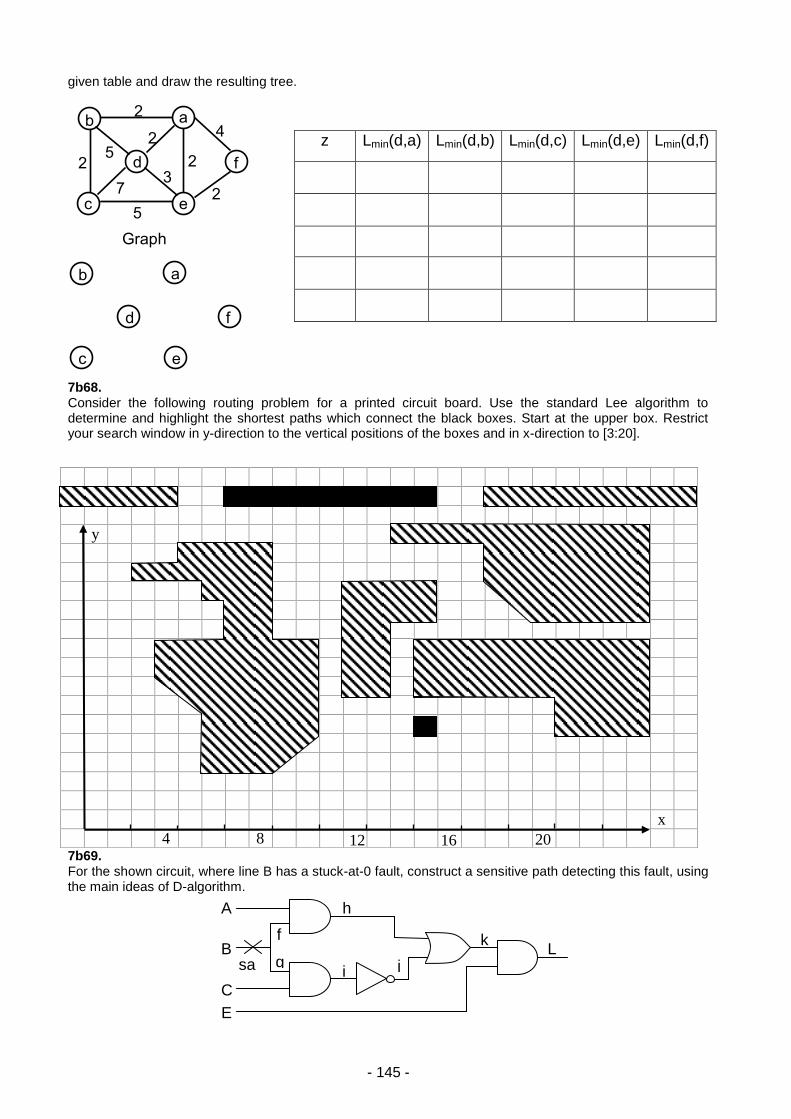
- 145 -
given table and draw the resulting tree.
7b68. Consider the following routing problem for a printed circuit board. Use the standard Lee algorithm to determine and highlight the shortest paths which connect the black boxes. Start at the upper box. Restrict your search window in y-direction to the vertical positions of the boxes and in x-direction to [3:20].
7b69. For the shown circuit, where line B has a stuck-at-0 fault, construct a sensitive path detecting this fault, using the main ideas of D-algorithm.
z Lmin(d,a) Lmin(d,b) Lmin(d,c) Lmin(d,e) Lmin(d,f)
y
x
4 8
A
B
C
E
sa0
f
g
h
i j
k L
12 16 20
Graph
a b
c
d
e
f 2
2
2
2
2
4
3 7
5
5
b
d
c e
a
f
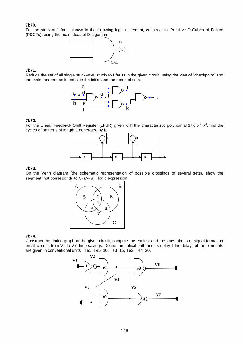
- 146 -
7b70. For the stuck-at-1 fault, shown in the following logical element, construct its Primitive D-Cubes of Failure (PDCFs), using the main ideas of D-algorithm.
7b71. Reduce the set of all single stuck-at-0, stuck-at-1 faults in the given circuit, using the idea of “checkpoint” and the main theorem on it. Indicate the initial and the reduced sets.
7b72. For the Linear Feedback Shift Register (LFSR) given with the characteristic polynomial 1+x+x
2+x
3, find the
cycles of patterns of length 1 generated by it.
7b73. On the Venn diagram (the schematic representation of possible crossings of several sets), show the
segment that corresponds to C⋅ (A+B) ՛ logic expression.
7b74. Construct the timing graph of the given circuit, compute the earliest and the latest times of signal formation on all circuits from V1 to V7, time savings. Define the critical path and its delay if the delays of the elements are given in conventional units: Te1=Te5=10, Te3=15, Te2=Te4=20.
e2 e3
e4 e5
V2
V3
V4
V5
V6
V7
V1
1
A B
C
5 2
1 3
6
4 7
x0
x1
x2
a
b
c
d
e
f
g h i
j
k
z
D
SA1
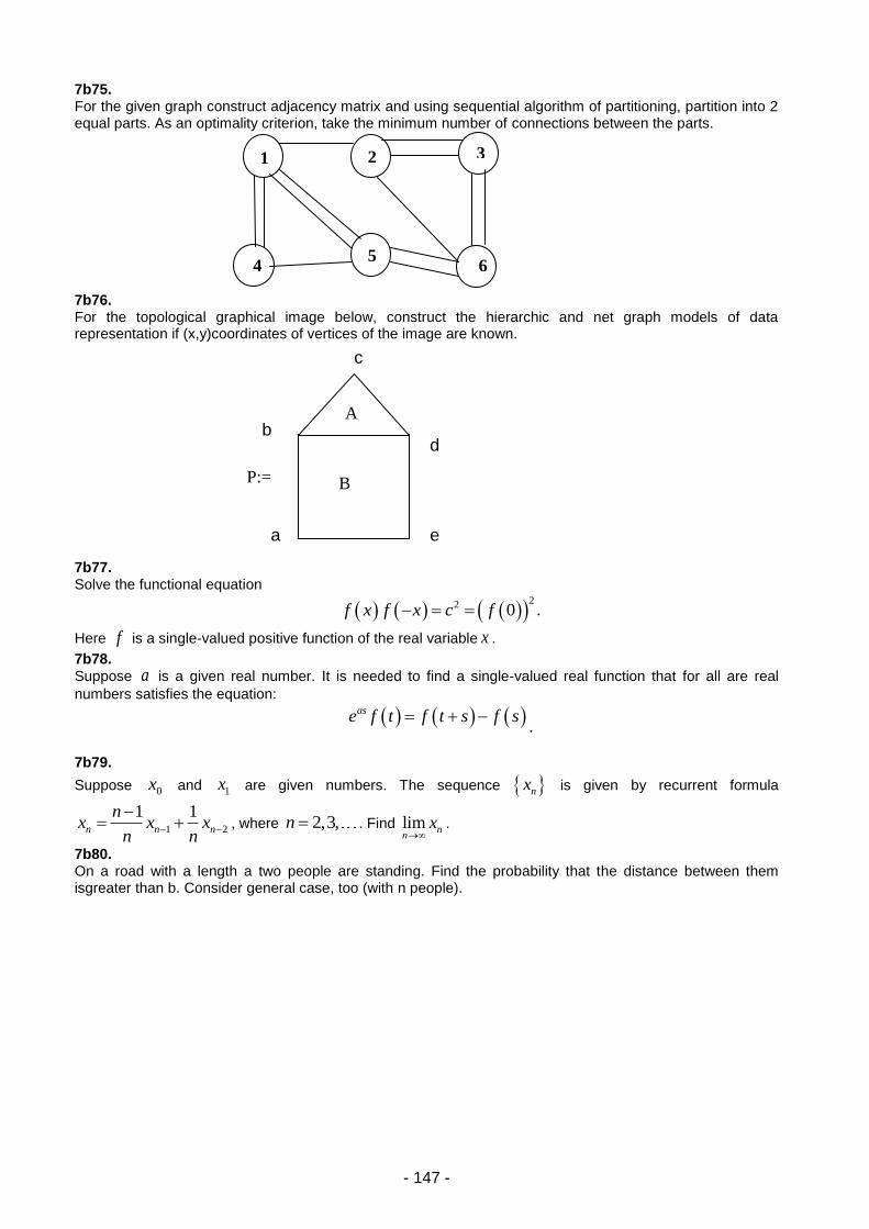
- 147 -
7b75. For the given graph construct adjacency matrix and using sequential algorithm of partitioning, partition into 2 equal parts. As an optimality criterion, take the minimum number of connections between the parts.
7b76. For the topological graphical image below, construct the hierarchic and net graph models of data representation if (x,y)coordinates of vertices of the image are known.
7b77. Solve the functional equation
22 0f x f x c f .
Here f is a single-valued positive function of the real variable x .
7b78. Suppose a is a given real number. It is needed to find a single-valued real function that for all are real
numbers satisfies the equation:
ase f t f t s f s .
7b79.
Suppose 0x and 1x are given numbers. The sequence nx is given by recurrent formula
1 2
1 1n n n
nx x x
n n
, where 2,3,n . Find lim n
nx
.
7b80. On a road with a length a two people are standing. Find the probability that the distance between them isgreater than b. Consider general case, too (with n people).
a
d
c
e
b
B
A
P:=
2
3 3
3 3
2
3
3 3
3 3
2
1
3 3
3 3
2
4
3 3
3 3
2
5
3 3
3 3
2
6
3 3
3 3
2

- 148 -
8. OBJECT-ORIENTED PROGRAMMING
a) Test questions 8a1. A function is formed that displays data (on
the screen) as well as writes them in the file. Referring to the scenario, which one of the following function declarations satisfies that need? A. void print(cout); B. void print(ostream &os); C. void print(istream &is); D. void print(ofstream ofs); E. void print(istream is);
8a2. After performing the below mentioned code, which is the value of n? int n = !(!5 & !7) A. false B. 1 C. 3 D. 5 E. It contains an error. After using !
operator, constant values should be definitely taken in brackets, e.g.(!5)
8a3. Small function is present, which is often called from several special places. How can the implementation of the codes be accelerated which use the given function? A. Make function virtual B. Replace floating point computation of
integer numbers, to use FPU device
C. Reduce the use of automat variables D. Make all the variables of that function
volatile E. Make function inline
8a4. Which is the difference between non-specialized function’s member and constructor? A. Constructor can return values, and
member-functions - no B. Member-functions can define values,
constructors – no. C. Constructor can define values, and
member-functions - no D. Member-functions can return values,
and constructors - no E. Constructor can announce values,
and member-functions - no
8a5. const int x= 0xFFFE; int y = 2; int z = x&&y; Which is the value of z, in terms of the above code? A. 0 B. 1 C. 2 D. 3 E. 4
8a6. Which of the below mentioned statements concerning overloading of ++ operator is true? A. It is impossible to overload prefix ++
operator B. It is impossible to overload postfix ++
operator C. It is necessary to use additional int
type parameter to overload ++ postfix operator
D. It is always necessary to create prefix ++ operator
E. It is impossible to overload both prefix and postfix ++ operators for one class.
8a7. Binary search complexity is A. O(logN), where N is the number of
elements B. O(NlogN) C. O(N) D. O(N
2)
E. The correct answer is missing
8a8. The complexity of Prim's algorithm is A. O(|E|) B. (|V|
2)
C. O(|E|*|V|) D. O(|E|+|V|) E. The correct answer is missing
8a9. When the class is inherited from base as public, which of the below mentioned statements is right? A. All the members of base class
become public members of inherited class
B. All the members of inherited class become public members of base class
C. All the protected members of base class are protected members of inherited class
D. All the members of base class become protected members of inherited class
E. All the members of inherited class become private members of base class
8a10. The ability to invoke a method of an object without knowing exactly what type of object is being acted upon is known as which one of the following? A. Encapsulation B. Class relationship C. Inheritance D. Polymorphism E. Friend relationship

- 149 -
8a11. class X
{
int I;
public:
int f() const;
};
int X::f() const {return I++;}
Where is an error in the above written code? A. X::f member-function must be static B. X::f member-function is constant but
changes non-mutable data-member of the object
C. X::I data-member lacks access specifier
D. X::f member-function cannot change as it lacks access specifier
E It is not possible to change the integer I as it lacks access specifier
8a12. The complexity of quick sorting algorithm for the worst case will be A. O(logN), where N is the number of
elements B. O(NlogN) C. O(N) D. O(N
2)
E. The correct answer is missing
8a13. class Base {
public:
Base();
~Base();
int getBaseNum();
private:
int baseNum;
};
class A : public Base{
public:
A();
~A()
float getBaseNum();
private:
float baseNum;
};
Which concept is presented through the code in the example? A. Recursion B. Polymorphism C. Inheritance D. Reloading of functions E. Virtual functions
8a14. int i = 4, x = 0;
do {
x++;
} while(i--);
What is the value of X after performing the above written code? A. 5 B. 4 C. 0 D. Infinite E. There is syntax error while cycle
cannot be formed as mentioned above
8a15. The complexity of Floyd algorithm is A. O(N
3), where N is the number of
nodes B. O(NlogN) C. O(N) D. O(N
2)
E. The correct answer is missing
8a16. The complexity of subline search in Knut-Morris-Pratt algorithm on average will be (n – length of the line, m – length of the subline) A. O(n) B. O(m) C. O(n+m) D. O(n*m) E. The correct answer is missing
8a17. class MyClass {
public:
MyClass();
virtual void MyFunction()=0;
};
Which is the below written statements is correct for the given code? A. MyClass is a pure virtual class B. Class definition is wrong C. MyClass is a virtual base class D. Function returns value E. MyClass is an abstract class
8a18. Which of the below written statements is correct for function overloading? A. Although the return type can be
modified, the types of the parameters can as well. The actual number of parameters cannot change.
B. Function overloading is possible in both C++ and C
C. Templates and namespaces should be used to replace occurrences of function overloading.
D. Overloaded functions may not be declared as "inline."
E. The compiler uses only the parameter list to distinguish functions of the same name declared in the same scope.
8a19. The complexity of Dexter algorithm is A. O(|E|) B. O(|E|*|V|) C. O(|V|
2)
D. O(|E|+|V|) E. The correct answer is missing
8a20. Assume an algorithm determines the number of triangles formed by n points in the plane. What is the maximal possible output of A for n=7? A. 35 B. 27 C. 17 D. 15 E. The correct answer is missing

- 150 -
8a21. What is the difference between class and struct? A. Class must contain constructor, and
struct may not have it B. Struct does not have inheritance
opportunity C. Struct does not have deconstructor D. By default input specificators are
distinguished E. No difference
8a22. Which is the value of z in case of the code below? const int x= 012; int z = 1 << x; A. 0 B. 1024 C. 4096 D. 2048 E. It contains an error and will get
compilation error
8a23. Which of the mentioned cycles is infinite? A. for (int i=1;i>23;i++); B. for (int i=0;i>=1;i++); C. for (int i=10;i>6;i++); D. for (int i=5;i>15;i++); E. All the cycles are finite
8a24. After performing the code below, what will be displayed on the screen? (assume sizeof(int) = 4) #include <iostream>
using namespace std;
void main(){
int (*p)[10]= {NULL};
int k= int((size_t)(p+1) -
(size_t)p);
cout<<k<<endl;
}
A. 1 B. 2 C. 4 D. 10 E. 40
8a25. Which of the mentioned ones is not heredity access attribute A. public B. private C. virtual D. protected E. All are heredity access attribute
8a26. For a given pair of integers n, k it is calculated n
k. Assuming that calculation
uses only multiplications, show the minimal number of multiplications among represented in the table that is enough to calculate 5
1024.
A. 12 B. 11 C. 10 D. 9 E. 8
8a27. After performing the code below, which is the value of n? int i = 5;
int n = i++-1;
A. 6 B. 5 C. 4 D. 3 E. It contains an error and will get
compilation error
8a28. After performing the code below, which is the value of b? #include <iostream>
using namespace std;
void main (){
int a = 0;
int b = 2;
switch (b) {
case 1:
a=1;
break;
case 2:
int b=0;
}
}
A. 0 B. 1 C. 2 D. There is syntax error, switch is not
possible to form as described above E. The program will work infinitely
8a29. Which of the mentioned is not C++ data type? A. unsigned long B. unsigned short C. unsigned char D. unsigned int E. All are C++ data types
8a30. Which of the mentioned is not one of the basic clauses of object-oriented programming? A. Encapsulation B. Typification C. Inheritance D. Polymorphism E. All the mentioned belong to the basic
clauses of object-oriented programming.
8a31. An algorithm is developed that for any given list of natural numbers L = {a1, …, an} finds the maximum, minimum elements and the arithmetical average value of L. What is the minimal number of passes in reading L that is enough get the output in the algorithm? A. 5 B. 4 C. 3 D. 2 E. 1
8a32. After performing the code below, which is the value of n? int n = 1 << 3 * 2 + 1;

- 151 -
A. 1 B. 17 C. 65 D. 128 E. It contains and error and will get
compilation error 8a33. To classify the following 1,2,3,5,4
sequence ascending, it is more appropriate to use A. Quick Sort B. Bubble Sort C. Merge Sort D. Heap Sort E. No appropriate version
8a34. After performing the code below, what will be displayed on the screen? #include <iostream>
using namespace std;
double A;
void main ()
{
int A;
A=5;
::A = 2.5;
cout<<A<<" "<<::A;
}
A. 5 2.5 B. 2.5 5 C. 5 5 D. 2.5 2.5 E. The program contains a syntax error
8a35. How much is the complexity of algorithm to add element in binary tree? A. O(N
2), where N is the number of
nodes B. O(logN) C. O(N) D. O(1) E. The correct answer is missing
8a36. An algorithm is developed that for any given list of natural numbers L = {a1, …,
an} finds the sum 2
1
n
i
i
a a( )
,
where a denotes the arithmetical
average of the elements list L: What is the floor amount of passes enough to calculate the output? A. 1 B. 2 C. 3 D. 4 E. 5
8a37. Which of the statements is correct? A. Class cannot have 2 constructors B. Class cannot have 2 destructors C. Virtual destructor does not exist D. All the above mentioned statements
are correct E. All the above mentioned statements
are wrong
8a38. The complexity of Merge Sort algorithm in the worst case will be: A. O(NLogN) B. O(N
2)
C. O(N) D. O(N
3)
E. The correct answer is missing 8a39. After performing the code below, what will
be displayed on the screen? #include <stdio.h>
class a {
public: virtual void print()
{printf("a");}
};
class b: public a{
public: virtual void print()
{printf("b");}
};
int main(){
b b0;
a a0= b0, &a1= b0;
a0.print();
a1.print();
return 0;
}
A. aa B. ab C. bb D. ba E. The program contains syntax error
8a40. After performing the code below, what will be displayed on the screen? #include <iostream>
using namespace std;
void main(){
int c = 1;
c= ++c + ++c;
cout<<c;
}
A. 2 B. 3 C. 4 D. 5 E. 6
8a41. What is the output of the following part of the program? cout << (2 | 4 ^ ~3 );
A. 0 B. 1 C. 2 D. 3 E. the correct answer is missing
8a42. How many errors are below? class B {}
class A
: public B
{
int m_value
int get_value(int = 0)
{
return m_value;

- 152 -
}
}
int main () {
A a();
a = a;
a.*get_value();
return 0;
}
A. 3 B. 4 C. 5 D. 6 E. 7
8a43. What is (7 >> 1 << 1) expression value? A. 5 B. 6 C. 7 D. 8 E. the correct answer is missing
8a44. What is the output of the following part of the program? int n = 5;
switch(n){
case '5':
cout << "A \n";
break;
case 5:
cout << "B \n";
default:
cout << "C \n";
break;
}
A. A B. B C. C D. BC E. AC
8a45. Complexity of “merge” sorting algorithm A. linear B. constant C. logn D. n*logn E. square
8a46. int n = !(!5 & !7)
What is the value of n after performing the code above? A. false B. true C. 0 D. 1 E. It has an error. Using ! operator,
constant values must be written in brackets. For example, (!5)
8a47. Complexity of adding element in search
balanced binary tree A. linear B. constant C. logn D. n*logn E. square
8a48. int i = 4, x = 0;
do{
x++;
}while(i--);
After executing the above written code, which is the value of X? A. 0 B. 1 C. 3 D. 4 E. 5 G.
8a49. class MyClass
{
public:
MyClass();
virtual void MyFunction()=0;
};
Which statement is true for the above
mentioned code?
A. Class definition is wrong B. MyClass is a virtual class C. MyClass is a virtual base class D. MyClass is an abstract class E. the correct answer is missing
8a50. What is the value of (13 >> 1 << 1) expression? A. 11 B. 12 C. 13 D. 14 E. 15
8a51. How many errors does the following part contain? class A
: int
{
int m_value
int get_value(int = 0)
{
return m_value;
}
}
int main () {
A a();
a = a;
a->get_value();
return 0;
}
A. 2 B. 3 C. 4 D. 5 E. 6
8a52. After performing the code below, what will
be displayed on the screen?
#include <iostream>
struct A {
virtual void f(int x = 0)
{
std::cout << "A: "
<< x << std::endl;

- 153 -
}
};
struct B : public A {
virtual void f(int x = 1)
{
std::cout << "B: "
<< x << std::endl;
}
};
int main()
{
A* p = new B();
p->f();
return 0;
}
A. A 0 B. A 1 C. B 0 D. B 1 E. The correct answer is missing
8a53. After performing the code below, what will
be displayed on the screen? #include <iostream>
struct A {
virtual ~A() {
std::cout << "A" <<
std::endl;
}
};
struct B : public A {
virtual ~B() {
std::cout << "B" <<
std::endl;
}
};
int main() {
A* p = new B();
delete p;
return 0;
}
A. A B. A B C. B D. B A E. The correct answer is missing
8a54. After performing the code below, what will
be displayed on the screen?
#include <iostream>
#include <memory>
void f(std::auto_ptr<int> a) {
*a = 3;
}
int main() {
std::auto_ptr<int> p(new
int(0));
f(p);
std::cout << *p <<
std::endl;
return 0;
}
A. 0 B. 3
C. The program contains compile-time error D. The program contains run-time error E. The correct answer is missing
8a55. After performing the code below, what will
be displayed on the screen?
#include <iostream>
struct Base {
virtual void f() {
foo();
}
virtual void foo() = 0;
};
struct Derived : public Base {
virtual void foo() {
std::cout << "Derived" <<
std::endl; }
};
int main() {
Base* pb = new Derived();
pb->f();
return 0;}
A. The program contains compile-time error as foo function has been called without description B. Derived C. Nothing D. The program contains run-time error E. The correct answer is missing
8a56. After performing the code below, what will
be displayed on the screen?
#include <iostream>
int main() {
int x = 1, y = 1;
if (x++ || y++) {
x += 5;
}
std::cout << y <<
std::endl;
return 0;
}
A. 1 B. 2 C. 5 D. 6 E. The correct answer is missing
8a57. After performing the code below, what will
be displayed on the screen?
#include <iostream>
struct A {
int m_x;
A(int x) : m_x(x) {
std::cout << m_x << " "; };
};
struct B : virtual public A {
B() : A(5) { }
};
struct C : virtual public A {
C() : A(0) { }

- 154 -
};
struct D : public B, public C {
D() : A(1) { }
};
int main() {
A* p = new D();
return 0;
}
A. 5 0 1 B. 0 1 C. 1 D. The program contains compile-time
error E. The correct answer is missing
8a58. After performing the code below, what will
be displayed on the screen?
#include <iostream>
void f(int& x) {
x += 3;
std::cout << x <<
std::endl;
}
int main() {
f(0);
return 0;
}
A. 0 B. 3 C. The program contains compile-time error D. The program contains run-time error E. The correct answer is missing
8a59. After performing the code below, what will
be displayed on the screen?
#include <iostream>
struct A {
int mx;
A(int x) : mx(0) { }
};
int main() {
A arr[5];
for (int i = 0; i < 3;
++i) {
std::cout <<
arr[i].mx << std::endl;
}
return 0;
}
A. 0 0 0 B. 5 5 5 C. 3 3 3 D. 3 3 3 0 0 E. The correct answer is missing
8a60. After performing the code below, what will
be displayed on the screen?
#include <iostream>
struct Exc1 {
void what() { std::cout
<< "Exc1" << std::endl; }
};
struct Exc2 : public Exc1 {
void what() { std::cout
<< "Exc2" << std::endl; }
};
int main() {
try {
throw Exc2();
} catch (Exc1& e) {
std::cout << "First
catch: ";
e.what();
} catch (Exc2& e) {
std::cout <<
"Second catch: ";
e.what();
} catch(...) {
std::cout <<
"Unknown exception" <<
std::endl;
}
return 0;
}
A. First catch Exc1 B. First catch Exc2 C. Second catch Exc2 D. Unknown exception E. The correct answer is missing
8a61. After performing the code below, what will be displayed on the screen? #include <iostream>
template <int i>
struct A {
static const int n =
i*A<i-1>::n;
};
template <>
struct A<1> {
static const int n = 1;
};
int main(){
std::cout << A<5>::n <<
std::endl;
return 0;
}
A. The program contains compile-time error B. 5 C. 24 D. 120 E. The correct answer is missing
8a62. Can the overloaded operator of the class be declared virtual? A. Yes B. No C. Only ++ and – operators D. Only if the class contains virtual destructor E. The correct answer is missing
8a63. After performing the code below, what will be displayed on the screen? #include <iostream>

- 155 -
#include <typeinfo>
struct A {};
struct B : public A {};
int main() {
A* p = new B();
std::cout <<
typeid(p).name() << std::endl;
return 0;
}
A. Struct A* B. Struct B* C. The program contains compile-time error D. The program contains run-time error E. The correct answer is missing
8a64. What design pattern is presented below? #include <iostream>
struct A {
virtual void f() {
func();
}
virtual void func() = 0;
};
struct B : public A {
virtual void func() {}
};
A. Virtual constructor B. Template method C. Strategy D. The program contains compile-time error E. The correct answer is missing
8a65. What design pattern is presented below? struct A {
virtual A* clone() {
return new A(*this); }
};
struct B : public A {
A* clone() { return new
B(*this); }
};
A. Virtual constructor B. Strategy C. Template method D. None E. The correct answer is missing
8a66. Which of the following class methods is not generated by compiler by default – in case of being not defined by the programmer? A. Default constructor B. Copy constructor C. Assignment operator D. Destructor E. The correct answer is missing
8a67. After performing the code below, what will be displayed on the screen? #include <iostream>
void f(int) { std::cout <<
"Integer" << std::endl; }
void f(unsigned short) {
std::cout << "Unsigned Short"
<< std::endl; }
void f(unsigned int) {
std::cout << "Unsigned Integer"
<< std::endl; }
int main() {
short c = 5;
f(c);
return 0;
}
A. Integer B. Unsigned Short C. Unsigned Integer D. The program contains compile-time error E. The correct answer is missing
8a68. After performing the code below, what will be displayed on the screen? #include <iostream>
#include <algorithm>
#include <functional>
struct A {
virtual void f() {
std::cout << "A "; }
};
struct B : public A {
virtual void f() {
std::cout << "B "; }
};
int main() {
A* a[] = { new A(), new
B() };
std::for_each(a, a+2,
std::mem_fun(&A::f));
return 0;
}
A. A A B. A B C. B A D. B B E. The correct answer is missing
8a69. What design pattern is presented below? struct AImpl {
void f() { }
};
class A {
AImpl* m_impl;
public:
A() : m_impl(new AImpl())
{ }
void f() { m_impl->f(); }
};
A. Virtual constructor B. Strategy C. Template method D. Bridge E. The correct answer is missing
8a70. What data-members can be initialized at declaration? A. Static B. Static const

- 156 -
C. Static const integral type D. None E. The correct answer is missing
8a71. Consider the following code: #include<iostream>
class A
{
public :
A()
{
std::cout <<
"Constructor of A\n";
};
~A()
{
std::cout <<
"Destructor of A\n";
};
};
class B : public A
{
public :
B()
{
cout <<
"Constructor of B\n";
};
~B()
{
cout << "Destructor
of B\n";
};
};
int main()
{
B* p;
p = new B();
delete p;
return 0;
}
What will be the printed output?
A. Constructor of B Constructor of A Destructor of A Destructor of B
B. Constructor of A Constructor of B Destructor of B Destructor of A
C. Constructor of B Constructor of A Destructor of B Destructor of A
D. Constructor of A Constructor of B Destructor of A Destructor of B
E. The sequence of construction and destruction of A and B will be compiler specific
8a72. Consider the sample code given below and
answer the question that follows. 1 class Car
2 {
3 private:
4 int Wheels;
5
6 public:
7 Car(int wheels = 0)
8 : Wheels(wheels)
9 {
10 }
11
12 int GetWheels()
13 {
14 return Wheels;
15 }
16 };
17 int main()
18 {
19 Car c(4);
20 cout << "No of wheels:"
<< c.GetWheels();
21 return 0;
22 }
Which of the following lines from the
sample code above are examples of data
member definition?
A. 4 B. 7 C. 8 D. 14 E. 19
8a73. What will happen when the following code
is compiled and executed? #include<iostream>
class my_class
{
private:
int number;
public:
my_class()
{
number = 2;
}
int& a()
{
return
number;
}
};
int main()
{
my_class m1, m2;
m1.a() = 5;
m2.a() = m1.a();
std::cout << m2.a();
return 0;
}

- 157 -
A. Compile time errors will be generated because right hand side of expressions cannot be functions
B. The printed output will be 5 C. The printed output will be 2 D. The printed output will be undefined E. None of the above
8a74. What will be the output of the following
code? class A
{
public:
A() : m_data(0){}
~A(){}
int operator ++()
{
m_data ++;
std::cout << "In first ";
return m_data;
}
int operator ++(int)
{
m_data ++;
std::cout << "In second ";
return m_data;
}
private:
int m_data;
};
int main()
{
A a;
std::cout << a++;
std::cout << ++a;
return 0;
}
A. In first 1 In second 2 B. In second 1In first 2 C. In first 0 In second 2 D. In second 0 In first 2 E. None of the above
8a75. What will be the output of the following
code? #include<iostream>
class b
{
int i;
public:
void vfoo()
{ std::cout <<"In Base "; }
};
class d : public b
{
int j;
public:
void vfoo()
{
std::cout<<"In Derived ";
}
};
int main()
{
b *p, ob;
d ob2;
p = &ob;
p->vfoo();
p = &ob2;
p->vfoo();
ob2.vfoo();
return 0;
}
A. In Base In Base In Derived B. In Base In Derived In Derived C. In Derived In Derived In Derived D. In Derived In Base In Derived E. In Base In Base In Base
8a76. Consider the following code: #include<stdio.h>
int main(int argc, char*
argv[])
{
enum Colors
{
red,
blue,
white = 5,
yellow,
green,
pink
};
Colors color = green;
printf("%d", color);
return 0;
}
What will be the output when the above
code is compiled and executed?
A. 4 B. 8 C. 16 D. 7 E. The code will have compile time
errors
8a77. Consider the sample code given below and
answer the question that follows. class SomeClass
{
int x;
public:
SomeClass (int xx) : x(xx) {}
};
int main()
{
SomeClass x(10);
SomeClass y(x);
return 0;
}

- 158 -
What is wrong with the sample code
above?
A. SomeClass y(x); will generate an error because SomeClass has no copy constructor
B. SomeClass y(x); will generate an error because SomeClass has no default constructor
C. SomeClass y(x); will generate an error because SomeClass has no public copy constructor
D. x(xx) will generate an error because it is illegal to initialize an int with that syntax
E. The code will compile without errors
8a78. Which of the following are NOT valid C++
casts? A. dynamic_cast B. reinterpret_cast C. static_cast D. const_cast E. void_cast
8a79. Consider the following code: class BaseException
{
public:
virtual void Output()
{
cout << "Base
Exception" << endl;
}
};
class DerivedException
: public BaseException
{
public:
virtual void Output()
{
std::cout <<
"Derived Exception" <<
std::endl;
}
};
void ExceptionTest()
{
try {
throw
DerivedException();
}
catch (BaseException&
ex) {
ex.Output();
} catch (...) {
cout <<
"Unknown Exception Thrown!" <<
endl;
}
}
Invoking Exception Test will result in which
output?
A. Base Exception B. Derived Exception C. Unknown Exception Thrown D. No Output will be generated E. None of the above
8a80. Consider the sample code given below and
answer the question that follows. class X {
int i;
protected:
float f;
public:
char c;
};
class Y : private X { };
Referring to the sample code above, which
of the following data members of X are
accessible from class Y?
A. c B. f C. i D. f and c E. None of the above
8a81.Which of the following sets of functions is
not qualified as overloaded function? A. void fun(int, char *)
void fun(char *, int) B. void x(int, char)
int *x(int, char) C. int get(int)
int get(int, int) D. void F(int *)
void F(float *) E. All of the above are overloaded
functions
8a82. Consider the sample code given below and
answer the question that follows. class Grandpa
{
} ;
class Ma : virtual public
Grandpa
{
} ;
class Pa : virtual public
Grandpa
{
} ;
class Me : public Ma, public
Pa, virtual public Grandpa
{
} ;

- 159 -
How many instances of Grandpa will each
instance of Me contain?
A. 1 B. 2 C. 3 D. 4 E. None of the above
8a83. What is the output of the following code
segment? int n = 9;
int *p;
p = &n;
n++;
cout << *p + 2 << ", " << n;
A. 11, 9 B. 9, 10 C. 12, 10 D. 11, 10 E. None of the above
8a84. Consider the sample code given below and
answer the question that follows: char** foo;
/* Missing code goes here */
for(int i = 0; i < 200; i++)
{
foo[i] = new char[100];
}
Referring to the sample code above, what
is the missing line of code?
A. foo = new *char[200] B. foo = new char[200] C. foo = new char[200]* D. foo = new char*[200] E. foo = new char[][200]
8a85. Consider the sample code given below and
answer the question that follows. class A
{
public:
A() {}
~A()
{
cout << "in destructor" << endl;
}
};
int main()
{
A a;
a.~A();
return 0;
}
How many times will "in destructor" be
output when the above code is compiled
and executed?
A. 0 B. 1 C. 2
D. A compile time error will be generated because destructors cannot be called directly
E. None of the above
8a86. Consider the sample code given below and
answer the question that follows. class Person
{
string name;
int age;
Person *spouse;
public:
Person(string sName);
Person(string sName,
int nAge);
Person(const Person& p);
Copy(Person *p);
Copy(const Person &p);
SetSpouse(Person *s);
};
Which one of the following are declarations
for a copy constructor?
A. Person(string sName) B. Person(string sName, int nAge) C. Copy(Person *p) D. Person(const Person &p) E. Copy(const Person &p)
8a87. Consider the following code. template<class T>
void kill(T *& t)
{
delete t;
t = NULL;
}
class my_class
{
};
void test()
{
my_class*ptr = new
my_class();
kill(ptr);
kill(ptr);
}
Invoking Test() will cause which of the
following?
A. Code will Crash or Throw and Exception
B. Code will Execute, but there will be a memory leak
C. Code will execute properly D. Code will exhibit undefined behavior E. None of the above
8a88. Which of the following is not a standard STL
header? A. <array> B. <deque> C. <queue> D. <list> E. None of the above

8a89. Which of the following member functions
can be used to add an element in an
std::vector?
A. add B. front C. push D. push_back E. None of the above
8a90. Consider the sample code given below and
answer the question that follows. class Shape
{
public:
virtual void draw() = 0;
};
class Rectangle: public Shape
{
public:
void draw()
{
// Code to draw rectangle
}
//Some more member
functions.....
};
class Circle : public Shape
{
public:
void draw()
{
// Code to draw circle
}
//Some more member
functions.....
};
int main()
{
Shape obj;
obj.draw();
return 0;
}
What happens if the above program is
compiled and executed?
A. Object obj of Shape class will be created
B. A compile time error will be generated because you cannot declare Shape objects
C. A compile time error will be generated because you cannot call draw function of class ‘Shape'
D. A compile time error will be generated because the derived class's draw() function cannot override the base class draw() function
E. None of the above
8a91. What is the output of the following C++
program?
#include <iostream>
class A
{
public:
explicit A(int n = 0) :
m_n(n) { }
A(const A& a)
: m_n(a.m_n)
{
++m_copy_ctor_calls;
}
public:
static int
m_copy_ctor_calls;
private:
int m_n;
};
int A::m_copy_ctor_calls = 0;
A f(const A& a) { return a; }
A g(const A a) { return a; }
int main()
{
A a;
A b = a, c(a);
std::cout <<
A::m_copy_ctor_calls;
b = g(c);
std::cout <<
A::m_copy_ctor_calls;
const A& d = f(c);
std::cout <<
A::m_copy_ctor_calls <<
std::endl;
return 0;
}
A. 245 B. 134 C. 124 D. Contains compile error E. None of the above
8a92. What is the output of the following C++
program?
#include <iostream>
#include <vector>
class A
{
public:
A(int n = 0) : m_n(n) { }
public:
virtual int value() const {
return m_n; }

- 161 -
virtual ~A() { }
protected:
int m_n;
};
class B
: public A
{
public:
B(int n = 0) : A(n) { }
public:
virtual int value() const {
return m_n + 1; }
};
int main()
{
const A a(1);
const B b(3);
const A *x[2] = { &a, &b };
typedef std::vector<A> V;
V y;
y.push_back(a);
y.push_back(b);
V::const_iterator i =
y.begin();
std::cout << x[0]->value()
<< x[1]->value()
<< i->value() <<
(i + 1)->value() << std::endl;
return 0;
}
A. 1313 B. 1413 C. 1423 D. Contains compile error E. None of the above
8a93. What is the output of the following C++
program?
#include <iostream>
class A
{
public:
A(int n = 2) : m_i(n) { }
~A() { std::cout << m_i; }
protected:
int m_i;
};
class B
: public A
{
public:
B(int n) : m_x(m_i + 1) ,
m_a(n) { }
public:
~B()
{
std::cout << m_i;
--m_i;
}
private:
A m_x;
A m_a;
};
int main()
{
{ B b(5); }
std::cout << std::endl;
return 0;
}
A. 2531 B. 5432 C. 2513 D. Contains compile error E. None of the above
8a94. What is the output of the following C++
program?
#include <iostream>
class A
{
public:
A() : m_i(0) { }
protected:
int m_i;
};
class B
{
public:
B() : m_d(0.0) { }
protected:
double m_d;
};
class C
: public A
, public B
{
public:
C() : m_c('a') { }
private:
char m_c;
};
int main()
{
C d;

- 162 -
A *b1 = &d;
B *b2 = &d;
const int a =
(reinterpret_cast<char*>(b1) ==
reinterpret_cast<char*>(&d)) ?
1 : 2;
const int b = (b2 == &d) ?
3 : 4;
const int c =
(reinterpret_cast<char*>(b1) ==
reinterpret_cast<char*>(b2)) ?
5 : 6;
std::cout << a << b << c <<
std::endl;
return 0;
}
A. 246 B. 135 C. 136 D. Contains compile error E. None of the above
8a95. What is the output of the following C++
program?
#include <algorithm>
#include <functional>
#include <iostream>
#include <iterator>
#include <list>
int main()
{
typedef std::list<int> L;
L l(5);
typedef L::const_iterator
CI;
CI cb = l.begin(), ce =
l.end();
typedef L::iterator I;
I b = l.begin();
std::transform(cb, --ce,
++b,
std::bind2nd(std::plus<CI::valu
e_type>(), 1));
std::copy(l.begin(),
l.end(),
std::ostream_iterator<CI::value
_type>(std::cout));
std::cout << std::endl;
return 0;
}
A. 01234 B. 43210
C. 12345 D. Contains compile error E. None of the above
8a96. What is the output of the following C++
program?
#include <cstddef>
#include <iostream>
class A
{
public:
A() : m_x(0) { }
public:
static ptrdiff_t
member_offset(const A &a)
{
const char *p =
reinterpret_cast<const
char*>(&a);
const char *q =
reinterpret_cast<const
char*>(&a.m_x);
return q - p;
}
private:
int m_x;
};
class B
: public A
{
public:
B() : m_x('a') { }
public:
static int m_n;
public:
static ptrdiff_t
member_offset(const B &b)
{
const char *p =
reinterpret_cast<const
char*>(&b);
const char *q =
reinterpret_cast<const
char*>(&b.m_x);
return q - p;
}
private:
char m_x;
};
int B::m_n = 1;
class C
{

- 163 -
public:
C() : m_x(0) { }
virtual ~C() { }
public:
static ptrdiff_t
member_offset(const C &c)
{
const char *p =
reinterpret_cast<const
char*>(&c);
const char *q =
reinterpret_cast<const
char*>(&c.m_x);
return q - p;
}
private:
int m_x;
};
int main()
{
A a;
B b;
C c;
std::cout <<
((A::member_offset(a) == 0) ? 0
: 1);
std::cout <<
((B::member_offset(b) == 0) ? 0
: 2);
std::cout <<
((A::member_offset(b) == 0) ? 0
: 3);
std::cout <<
((C::member_offset(c) == 0) ? 0
: 4);
std::cout << std::endl;
return 0;
}
A. 1234 B. 0204 C. 1230 D. Contains compile error E. None of the above
8a97. What is the output of the following C++
program?
#include <iostream>
template<class T, T t = T()>
class A
{
private:
template<bool b>
class B
{
public:
static const int m_n =
b ? 1 : 0;
};
public:
static const int m_value =
B<(t > T())>::m_n - B<(t <
T())>::m_n;
};
int main()
{
std::cout << A<int, -
9>::m_value << A<bool,
true>::m_value
<<
A<char>::m_value << std::endl;
return 0;
}
A. -110 B. 101 C. -101 D. Contains compile error E. None of the above
8a98. What is the output of the following C++
program?
#include <iostream>
class A
{
public:
A(int n = 0)
: m_i(n)
{
std::cout << m_i;
++m_i;
}
protected:
int m_i;
};
class B
: public A
{
public:
B(int n = 5) : m_a(new
A[2]), m_x(++m_i) { std::cout
<< m_i; }
~B() { delete [] m_a; }
private:
A m_x;
A *m_a;
};
int main()
{
B b;
std::cout << std::endl;

- 164 -
return 0;
}
A. 02020 B. 20020 C. 02002 D. Contains compile error E. None of the above
8a99. What is the output of the following C++
program?
#include <iostream>
class A
{
public:
virtual void f(int n) {
std::cout << n << 1; }
virtual ~A() { }
void f(int n) const {
std::cout << n; }
};
class B
: public A
{
public:
void f(int n) { std::cout
<< (n << 1); }
void f(int n) const {
std::cout << n + 1; }
};
int main()
{
const A a;
B b;
A &c = b;
const A *d = &b;
a.f(2);
b.f(2);
c.f(1);
d->f(1);
std::cout << std::endl;
return 0;
}
A. 2421 B. 4131 C. 2411 D. Contains compile error E. None of the above
8a100. What is the output of the following C++
program?
#include <algorithm>
#include <iostream>
#include <list>
#include <vector>
class Int
{
public:
Int(int i = 0) : m_i(i) { }
public:
bool operator<(const Int&
a) const { return this->m_i <
a.m_i; }
Int& operator=(const Int
&a)
{
this->m_i = a.m_i;
++m_assignments;
return *this;
}
static int
get_assignments() { return
m_assignments; }
private:
int m_i;
static int m_assignments;
};
int Int::m_assignments = 0;
int main()
{
std::list<Int> l;
l.push_back(Int(3));
l.push_back(Int(1));
l.sort();
std::cout <<
Int::get_assignments();
std::vector<Int> v;
v.push_back(Int(2));
v.push_back(Int());
std::sort(v.begin(),
v.end());
std::cout <<
Int::get_assignments() <<
std::endl;
return 0;
}
A. 20 B. 00 C. 02 D. Contains compile error E. None of the above
8a101. What is the output of the following C++
program?
#include <algorithm>
#include <iostream>
#include <list>

- 165 -
struct P
{
bool operator()(const int
&n) const
{
return n % 3 == 0;
}
};
int main()
{
const int a[] = { 5, 2, 6,
1, 13, 9, 19 };
const int count = sizeof(a)
/ sizeof(a[0]);
std::list<int> l(a, a+
count);
std::cout << l.size();
std::remove_if(l.begin(),
l.end(), P());
std::cout << l.size() <<
std::endl;
return 0;
}
A. 66 B. 77 C. 44 D. Contains compile error E. None of the above
8a102. What is the output of the following C++
program?
#include <iostream>
#include <stdexcept>
class A
{
public:
A(int n) : m_n(n) {
std::cout << m_n; }
~A() { std::cout << m_n; }
private:
int m_n;
};
int f(int n)
{
if (1 == n) {
throw
std::logic_error("0");
}
A l(n);
return f(n - 1) * n / (n -
1);
}
int main()
{
try {
int r = f(3);
A a(r);
}
catch (const std::exception
&e) {
std::cout << e.what()
<< std::endl;
}
return 0;
}
A. 32230 B. 03223 C. 32023 D. Contains compile error E. None of the above
8a103. What is the output of the following C++
program?
#include <iostream>
class A
{
public:
A(int i) : m_i(i) { }
public:
int operator()(int i = 0)
const { return m_i + i; }
operator int () const {
return m_i; }
private:
int m_i;
friend int g(const A&);
};
int f(char c)
{
return c;
}
int g(const A& a)
{
return a.m_i;
}
int main()
{
A f(2), g(3);
std::cout << f(1) << g(f)
<< std::endl;
return 0;
}
A. 53 B. 33 C. 35 D. Contains compile error E. None of the above

- 166 -
8a104. What is the output of the following C++
program?
#include <iostream>
class A
{
public:
explicit A(int n = 0) :
m_n(n) { }
public:
A& operator=(const A& a)
{
this->m_n = a.m_n;
++m_assignment_calls;
return *this;
}
public:
static int
m_assignment_calls;
private:
int m_n;
};
int A::m_assignment_calls = 0;
A f(const A& a) { return a; }
A g(const A a) { return a; }
int main()
{
A a(3);
A b = a;
std::cout <<
A::m_assignment_calls;
b = g(a);
g(b);
std::cout <<
A::m_assignment_calls;
const A& c = f(b);
std::cout <<
A::m_assignment_calls <<
std::endl;
return 0;
}
A. 110 B. 101 C. 011 D. Contains compile error E. None of the above
8a105. What is the output of the following C++
program?
#include <iostream>
class A
{
public:
A(int n = 0) : m_n(n) { }
A(const A &a) : m_n(a.m_n)
{ ++m_copy_ctor_calls; }
~A() { ++m_dtor_calls; }
private:
int m_n;
public:
static int
m_copy_ctor_calls;
static int m_dtor_calls;
};
int A::m_copy_ctor_calls = 0;
int A::m_dtor_calls = 0;
int main()
{
A *p = 0;
{
const A a = 2;
p = new A[3];
p[0] = a;
}
std::cout <<
A::m_copy_ctor_calls <<
A::m_dtor_calls;
p[1] = A(1);
p[2] = 2;
delete [] p;
std::cout <<
A::m_copy_ctor_calls <<
A::m_dtor_calls << std::endl;
return 0;
}
A. 0106 B. 6100 C. 0601 D. Contains compile error E. None of the above
8a106. What is the output of the following C++
program?
#include <iostream>
class B
{
public:
virtual int shift(int n =
2) const { return n << 2; }
};
class D
: public B
{
public:
int shift(int n = 3) const
{ return n << 3; }
};
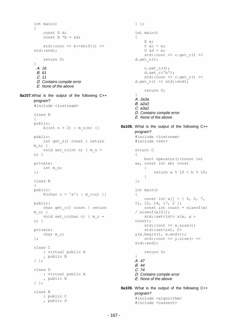
- 167 -
int main()
{
const D d;
const B *b = &d;
std::cout << b->shift() <<
std::endl;
return 0;
}
A. 16 B. 61 C. 11 D. Contains compile error E. None of the above
8a107.What is the output of the following C++
program?
#include <iostream>
class A
{
public:
A(int n = 2) : m_n(n) {}
public:
int get_n() const { return
m_n; }
void set_n(int n) { m_n =
n; }
private:
int m_n;
};
class B
{
public:
B(char c = 'a') : m_c(c) {}
public:
char get_c() const { return
m_c; }
void set_c(char c) { m_c =
c; }
private:
char m_c;
};
class C
: virtual public A
, public B
{ };
class D
: virtual public A
, public B
{ };
class E
: public C
, public D
{ };
int main()
{
E e;
C &c = e;
D &d = e;
std::cout << c.get_c() <<
d.get_n();
c.set_n(3);
d.set_c('b');
std::cout << c.get_c() <<
d.get_n() << std::endl;
return 0;
}
A. 2a3a B. a2a3 C. a3a2 D. Contains compile error E. None of the above
8a108. What is the output of the following C++
program?
#include <iostream>
#include <set>
struct C
{
bool operator()(const int
&a, const int &b) const
{
return a % 10 < b % 10;
}
};
int main()
{
const int a[] = { 4, 2, 7,
11, 12, 14, 17, 2 };
const int count = sizeof(a)
/ sizeof(a[0]);
std::set<int> x(a, a +
count);
std::cout << x.size();
std::set<int, C>
y(x.begin(), x.end());
std::cout << y.size() <<
std::endl;
return 0;
}
A. 47 B. 44 C. 74 D. Contains compile error E. None of the above
8a109. What is the output of the following C++
program?
#include <algorithm>
#include <cassert>

- 168 -
#include <cstddef>
#include <functional>
#include <iostream>
#include <vector>
class A
{
public:
A() : m_size(sizeof(A)) { }
public:
virtual void f() const {
std::cout << 1; }
virtual ~A() { }
public:
static bool compare(const A
*a, const A *b)
{
assert(a != 0);
assert(b != 0);
return a->m_size < b-
>m_size;
}
protected:
size_t m_size;
};
class B
: public A
{
public:
B() : m_b(0) { m_size =
sizeof(B); }
public:
virtual void f() const {
std::cout << 2; }
private:
char *m_b;
};
class C
: public A
{
public:
C() { m_size = sizeof(C); }
public:
virtual void f() const {
std::cout << 3; }
public:
static int *m_c;
};
int *C::m_c = 0;
struct D
{
void operator()(A *a) const
{ delete a; }
};
int main()
{
typedef std::vector<A*> V;
V v;
v.push_back(new C);
v.push_back(new B);
v.push_back(new A);
std::stable_sort(v.begin(),
v.end(), A::compare);
std::for_each(v.begin(),
v.end(), std::mem_fun(&A::f));
std::cout << std::endl;
D d;
std::for_each(v.begin(),
v.end(), d);
return 0;
}
A. 123 B. 312 C. 231 D. Contains compile error E. None of the above
8a110. What is the output of the following C++
program?
#include <iostream>
class A
{
public:
A(int n = 0) : m_i(n) {
std::cout << m_i; }
protected:
int m_i;
};
class B
: public A
{
public:
B(int n) : m_j(n) , m_a(--
m_j) , m_b() { std::cout <<
m_j; }
private:
int m_j;
A m_a;
A m_b;
static A m_c;
};
int main()
{
B b(2);
std::cout << std::endl;
return 0;
}
A B::m_c(3);
A. 30101 B. 30103 C. 00101 D. Contains compile error E. None of the above

- 169 -
b) Problems 8b1. Develop a program that, given two symbol sequences, finds the length of the longest common subsequence of the given sequences For example,
SYNOPSYS, SINOPSYS 7 8b2. Assume A is the known W. Ackermann function:
(0, ) 1;
( ,0) ( 1,1);
( 1, 1) ( , ( 1, )).
A y y
A x A x
A x y A x A x y
Redefine A in a way that it is computed modulo 7717.
( , ) ( , ) (7717),AM x y A x y Mod Restrict the enormous growth of A. Develop a program that can compute AM(10,10) in several seconds and find the value of AM(10,10). 8b3.
Assume Fib is the Fibonacci function:
otherwise. ),2()1(
2nor 1n if ,1)(
nFibnFibnFib
Define the number Q as follows: .)k(FibFib/1Q
11
1k
Calculate the number Q with an accuracy guaranteeing that the sum of the first 36 decimal digits can be computed exactly. 8b4. Develop an algorithm that for any given pair of natural numbers n ≥ k constructs the set of all the subsets of {1,2,…,n} having cardinality equal to k. 8b5. Prove (using induction argument) that the following algorithm for exponentiation is correct. function power (y,s)
comment Return yz, where уR, z N
x:=1; while z > 0 do if z is odd then x := x * y;
z:= z/2; y:=y2; return(x) 8b6. Prove (using induction argument) that the following algorithm for the multiplication of natural numbers is correct. function multiply (y, z)
comment Return у*z, where y,z N x:=0: while z > 0 do x := x + y * (z mod 2);
y:=2y; z:= z/2; return(x) 8b7. Prove (using induction argument) that the following algorithm for the multiplication of natural numbers is correct. function multiply(y, z) comment Return the product y*z. If z = 0 then return(0) else
return(multiply(2y, z/2 + y*(z mod 2)) 8b8. Write a program which, given a sequence of integers, finds the length of the longest increasing subsequence. Input Input contains length of sequence 0<N<1000, then follows N integers, does not exceed 109 by absolute.

- 170 -
Output Write one number in the output, length of the longest increasing subsequence. Example Input Output 5 1 7 1 5 2 3 3 8b9. Assume F is a Fibonacci sequence. F0 = 1; F1 = 1; FN = FN-1 + FN-2 N>1 Write a program to find N-th Fibonacci number modulo 1000007. 0 < N < 109 Example N = 5 F5 % 1000007 = 8 8b10. Given a positive integer N. Write a program to count the number of positive integers, not exceeding N and not divisible none of the given integers: 2,3,5. Input Input contains one integer N (1≤N≤2000000000). Output Output one number, answer for the given N. Example Input Output 10 2
8b11. Develop a detailed flowchart for an algorithm computing the greatest common divisor for a pair of positive integers, avoiding deletion operation.
8b12.
Assume a digital image is given by means of M = ||m ij || nn matrix where mij are non-negative integers. a. Develop a detailed flowchart for an algorithm that finds the (rounded) coordinates of the centre of gravity of the image. Define needed auxiliary functions. b. Evaluate the complexity of the developed algorithm.
8b13.
Assume for any integer m 2 P(m) is a result of attaching consecutive positive integers represented in m-ary form. For example, the beginning part of P(3) looks as follows:
Develop a detailed flowchart for an algorithm that given m 2 and n 1 finds the numeral allocated at n-th place in P(m) . Define needed auxiliary functions.
8b14. A sequence is said to be a polyndrome if it has the central symmetry. Develop a detailed flowchart for an algorithm that given binary sequence S finds а longest segment of S that is a palindrome. If there are several such segments then it is enough to find one of them and the length of it.
8b15. Print out all simple numbers not exceeding 1000. Natural number is called simple if it has exactly two dividers.
8b16. Print out all perfect numbers not exceeding 1000. Natural number is called perfect if it equals the sum of all its dividers. For example, 6 = 1 + 2 + 3.
8b17. Check if the given n number is symmetric or not (n < 107). The number is symmetric if it is read the same way from the beginning and the end. For example, 7586857.
8b18.
Let n2 be an integer. A partition of n is a representation of n as a sum of positive integers without taking their order into account. For example, the partitions of 3 are:
1 2 10 11 12 20 21 22 100 101 110
L 1 2 3 4 5 6 7 8 9 10 11
- 171 -
1+1+1; 2+1; 3.
Develop a pseudocode for an algorithm generating the list of all the partitions of the given n.
8b19.
Binomial coefficients ( ) are defined as follows: (
)
( )
Assume that admissible arithmetical operations are addition, subtraction, multiplication and division. Assuming that multiplication and division operations have the same complexity, and neglecting addition and subtraction operations, do the following.
A. Write a pseudocode for trivial, direct calculation of binomial coefficients. B. Propose a faster algorithm for calculation of binomial coefficients and develop a pseudocode. C. Evaluate the complexities C1(n,m) and C2(n,m) of the developed codes. D. Find, how faster your own algorithm’s code works with respect to the trivial one for n=100 and m=90.
8b20. The array coefficients An = [an , an-1 , .. . a1
, a0] are associated with a random polynomial An(x) = an x
n + an-1
xn-1
+ . . . + a1 x + a0.
A. Develop an algorithm that given polynomial coefficients arrays An = [an , an-1 , .. . a1 , a0] and
Bm = [bm , bm-1 , .. . b1 , b0] calculates the array corresponding the product An(x) * Bm(x).
B. Develop a detailed flowchart for that algorithm.
8b21. The sequence P(n) represents monotonically ordered integer powers and sums of those powers of the number 5. For simplification, the initial segment of P(n) is as follows: 1, 5, 6, 25, 26, 30, 37,125, ... Develop a detailed flowchart for an algorithm that calculates P(n). 8b22. Assume given two rectangles – with top left vertex and bottom right vertex coordinates. Implement a program that will detect the crossing of those rectangles.
8b23. Assume the number of vertices of convex polygon is given. No three diagonals of a convex polygon cross in one point. Develop a program that finds the number of crossing points of polygon’s diagonals.
The number of crossing points of diagonals is equal to 5.
8b24. Develop a program that will check whether the given polygon is convex or not. A convex polygon is a simple polygon interior of which is a convex set. The following properties of a simple polygon are all equivalent to convexity: Every internal angle is less than 180 degrees. Every line segment between two vertices remains inside or on the boundary of the polygon. Otherwise, the polygon is called concave.
(0, 15)
(20,0)
(-5,8)
(10,-20)
(0, 8)
(10, 0)
- 172 -
8b25. Assume given a MxN rectangle in a unit grid. Develop a program that will find all rectangles within the given rectangle, the vertices of which are the nodes of the grid, and the sides of which are parallel to the coordinate axis.
Example: For the 2x3 rectangle given above, the result is 18 rectangles. 8b26. Write a program which will set the natural number n and will print the count of n digit numbers which are relatively prime with 30 (the numbers are called relatively prime if they have no common positive divisor other than 1, for example 7 and 30). For example if input number is 1, the output will be 2. 8b27. Write a program which will set the natural number n and will print the count of last zeros of number n! (n! = n*(n-1)*…*1). For example if input is 5, the 5! = 120 ends by one zero, therefore the output will be 1. 8b28. Write a program which will set the natural number n and will print the sum of all n digit numbers the digits of which are 1, 2, 3, 4, and 5. For example if input number is 1, the output will be 15. 8b29. Write a program which will set the natural number n and will print the count of n digit numbers that contain digits 1 and 2. For example if input number is 2, the output will be 34. 8b30. Given is the following sequencing graph of an algorithm. The edges describe the data-dependencies between the operations such that an operation may only be executed after all its predecessors in the sequencing graph finished execution. The available functional units are an adder and a multiplier. The adder has a latency of one clock cycle and the multiplier of two clock cycles.
Determine the start times of all operations using the as-soon-as-possible scheduling (ASAP) method. What is the latency of this schedule? How many operational units are required for this schedule? 8b31. Given matrix A(nxm) of rows and all columns of which are sorted, i.e. for all valid i and j A[i][j] < A[i][j+1] and A[i][j] < A[i+1][j]. Write a program which takes matrix A and k elements c1,...,ck numbers as an input and for each ci prints the following “dose ci exist in matrix A” at the output. 8b32. Left rotation of a string is to move some leading characters to its tail. Implement a function to rotate a string. For example, if the input string is “abcdefg” and number 2, the rotated result is “cdefgab”. Write a
program which rotates given string with given length n by given number c (c < n).
8b33. Write a program which takes given natural numbers M, N, and a1, …, aM integral numbers and prints the N minimum numbers. For example, if the given numbers are 5, 2, and {4, 5, 6, 2, 8}, the output must be {2, 4}.
convex concave
NOP
NOP
V0
V1 V2 V3
V4 V5
V6
V7
*
*
* *
+
+

- 173 -
8b34. There are N doors in a row numbered from 1 to N. Initially all doors are closed. N passes are made by the N doors. In pass 1 all the doors (1,2,3,4....) are toggled starting from the first door. In the second pass every second door is toggled (2,4,6,8,...). In the third pass every third door is toggled (3,6,9...). Similarly N passes are made. Write a program which takes natural numbers N and k and prints the state of door k after N passes, i.e. “Open” or “Close”.

- 174 -
9. NANOELECTRONICS
a) Test questions 9a1. What are the conditions that minimum
energy change of contact potential must satisfy to notice one electron-tunneling? A. Must be smaller than temperature fluctuation B. Must be larger than quantum fluctuation C. Must be larger than temperature fluctuation D. Must be larger than potential barriers E. B) and C) together
9a2. Why is size quantization phenomena
more accessible and easier observed in semiconductors than the metals? A. Charge carriers’ density in
semiconductors is small B. Semiconductors can be doped by mixtures C. The effective electron mass and energy in semiconductors are small D. Charge carriers’ density in metals is large E. Charge carriers’ mobility in semiconductors is small
9a3. What model is required to be used considering size quantization phenomena in a MOS transistor in deep inverse mode? A. Rectangular infinite well model B . Rectangular finite well model C. Short channel phenomena model D. Full depletion mode model E. Triangular well model
9a4. In order to overcome Columb blockade, voltage must be applied which should be A. Larger than potential barriers value B. Smaller than potential barriers value C. Equal to D. Larger than E. A) and D) together
9a5. What are the zone marginal bendings in hyper networks (eg. GaAs) conditioned by? A. Difference of bandgap prohibited zones B. Difference of output work C. Interrelation difference towards
electron D. Concentration of mixtures E. Charged different depletion layers,
following each other
9a6. Mark the wrong answer for carbon nanopipes: A. Carbon nanopipe is the third subtype of
carbon B. Carbon nanopipe is a molecule,
consisting of one of the various atoms of carbon
C. Carbon nanopipe is a pipe with up to 1nm in diameter and several um roller tube
D. Carbon atoms are arranged in the plane of separate layers in carbon nanopipes
E. Carbon atoms are arranged on the vertices of regular six-angles on the walls of carbon nanopipes.
9a7. What is atomic force microscope
operation based on? A. The intermolecular interactions in case
of angstrom sized distances between probe and the surface
B. The intermolecular interactions in case of micrometer sized distances between probe and the surface
C. The intermolecular interactions in case of several dozen nanometers sized distances between probe and the surface
D. The registration of the tunnel current between probe and the surface
E. The optical interactions between the probe and surface
b) Problems
9b1
It is known that colloidal solutions (sols), for example, quantum dots, can agglomerate, forming composite
complexes, consisting of 2 or more particles. One reason for this phenomenon is the excess surface energy
and the power of molecular attraction, forcing other small particles to unite. To prevent agglomeration, it is
possible to report the charge of the same name sign to nanoparticles, which will lead to their repulsion. How
can nanoparticles be charged in a colloidal solution ? What could be the minimum and maximum charge of
nanoparticles? Suppose, for example, each of the forming sols of silicon nanocrystals (Si), having a
spherical shape with a radius R = 1 nm, and a positive charge q, equal in magnitude to twice the electron
charge was reported. Will these particles form agglomerates in a collision in a colloidal solution in benzene at
room temperature? Will the result change if benzene is replaced with water? Does the probability of
- 175 -
agglomeration depend on size of the nanoparticle, their concentration, the temperature of the solution?
Charged colloidal nanoparticles
9b2
At present, many types of light sources are known. However, few know that the work of any of them is
impossible without the use of nanotechnology. Moreover, the more informed a person is using
nanotechnology to create a light source, the more sophisticated, versatile and reliable they become.
Historically, the first light source for humans was the fire. Sitting in a cave near the fire, the old man
indifferently followed how under the influence of ascending air currents, nanoparticles ash and soot, smoke
generators, moved into aerosol state and evaporated back.
1) Calculate the upward air flow V speed, which is necessary for translation of spherical nanoparticles of
carbon with a diameter of 100 nm into aerosol state, if (coefficient of internal friction of particles) is
equal to 0.72, outhezia force F (which determines the particle sedimentation) 0.4 N, the resistance
coefficient of particles equal to 107, particle density is taken as 1.17 g/cm
3.
Note: for calculation use v = (2F/cS)1/2
, where S = area of cross-section of the particle.
The next generation light sources were incandescent lamps. The work of such light sources is based on a
tungsten (wolfram) filament that glows because of warm-up from passing of electric current through it. The
lifetime of the lamp is small. However, it was found that the addition of halogens into a lamp (especially
iodine) significantly prolongs the lifetime of the light source (the so-called halogen lamps). Special research
has shown that the lifetime of the lamp in this case is due to the chemical transport reactions involving
formed intermediate compounds nanoclusters of tungsten and halogen.
2) One of such nanoclusters has composition W6I12 and is characterized by an ionic structure.
Experimentally it is stated that under the action of silver nitrate, only 1/3 of the total amount of iodine
can be precipitated of the nanoclusters. Suggest a nanocluster structure. Note that the cation in the
nanocluster has high-symmetric structure.
The main drawback of incandescent lamps - the enormous loss of energy in the form of useless heat
dissipation. As an alternative to incandescent lamps mercury (Hg) lamps can be seen, in which the sources
of light radiation are the mercury atoms, excited by a glow electric discharge. The main disadvantage of such
lamps - the complexity of their utilization.
3) Suggest a reasonable means of utilizing mercury lamps by means of nanotechnology. Note that the
proposed method should be simple, economically viable and exclude any risk for the environment.
The most advanced light sources (LED lamps) are based on the luminescence of quantum dots. Their main
peculiarity is that, by varying the size of nanoparticles of luminescent material, radiation with different
energies and, consequently, with different wavelengths can be obtained.
4) What color will light LED lamp based on quantum dots of cadmium selenide radius of 3 nm? For
calculation use (Eg)2 = (E0)
2 + [2(h/2)
2E0(/r)
2] / m, where Eg – gap width for a quantum quantum
dot, E0 - the band gap for the bulk sample, r - radius of the nanocrystal (m), m - electron effective
mass. For CdSe E0 = 2.8810-19
J, m = 1.0910-31
kg.
9b3
In a nanoworld there is everything - even machines that can transport molecules, clusters and other nanogoods or simply ride without business. Imagine a nano-vehicle, in which the roles of front and rear pairs of wheels do the same nanotube, closed on both sides (Fig. 1).
Fig.1. Nano-vehicle on nano-wheels
Fig.2. Section of a wheel (N = 8)
- 176 -
The wheels of such a vehicle are not perfect cylinders. They are composed of hexagons with a side of 0.14 nm, and the cross section is not a circle, but correct N-gon (Fig. 2). When moving, the truck will keep on hopping, spending energy mgh on each jump, where m - mass of the truck, h - the height of the jump, which depends on the number of hexagons in a section of the wheel – N.
The mass of nano-truck for large N can be described by: m(N) = m1 + m2N + m3N2, where m1 = 10
000 a.m.u. (atomic mass unit), m2 = 700 a.m.u., m3 = 25 a.m.u.
1) Explain the type of dependence m(N) . 2) Determine the dependence of the energy E required for one step, from N . 3) Determine the value of N, for which the energy wastes in one step are minimal, and calculate these
costs.
Consider that for small angles, the approximate expressions for trigonometric functions can be used: sin(x) ≈ x, cos(x) ≈ 1 – x
2/2.
9b4
A quantum dot is a semiconductor nanocrystal, in which the movement of charges is limited to three dimensions in space. In a bulk semiconductor material there exists valence band and conductivity band, separated from one another by band gap. If the electron energy increases, it passes into the conductivity band and a hole appears in valence band. In a quantum dot instead of bands, there are discrete levels, and the band gap (Eg) in this case is the difference of higher energy filled and lowest unoccupied electronic levels.
1) Qualitatively sketch the energy band diagram for the bulk semiconductor and the quantum dot. In both figures, mark the band gap.
2) What is a hole? It was found that wavelength of luminescence and band gap are related for quantum dots:
(Eg)2 = (E0)
2 + [2(h/2)
2E0(/r)
2] / m, where Eg – gap width for a quantum dot, E0 - the band gap for
the bulk sample, r - radius of the nanocrystal (m), m - effective mass of electron. For cadmium
selenide E0 = 2.8810-19
J, m = 1.0910-31
kg. 3) What is the luminescence? 4) Calculate what is the wavelength of the luminescence (assuming that it corresponds to the band gap)
for a crystal with 1 cm radius, 1 nm equal to. 5) What is the minimum size of the quantum dot that corresponds to the luminescence in the visible
range? Find the required data.
One way of obtaining nanoparticles of cadmium selenide is the interaction of cadmium oleate Cd(C17H33COO)2 and trioctilephosphinselenide SeP(C8H17)3 in the environment of diphenyl ether (C6H5)2O.
The reaction is carried out by heating up to 200C for 5 minutes in an argon atmosphere, then cooled to room temperature. The obtained quantum dots of cadmium selenide are precipitated with acetone.
6) Write the reaction equation of obtaining quantum dots as per the above written method. 7) Why such specific conditions (argon atmosphere, reagents, solvents) are needed for the reaction?
Maybe it is easier to pour hot water solutions of salts of cadmium and appropriate selenide? 8) Where quantum dots, based on cadmium selenide, can be (or are already) applied?
9b5
Once, two young friend-nanotechnologists asked, at first glance, a simple question: how does the de Broglie wave frequency ω of free particle depend on wave vector k? They decided to get the right formula, but each of them acted in his own way.
The first one thought this way. Write the well-known formula of connection (cyclic) frequency with the period:
2
T
. Express the period through the wavelength and speed: T
. In the result, this is obtained:
2 2
T
(1)
Then apply the de Broglie relation for the pulse and wavelength: h
p . Substitute it in (1), after which
consider 2h , and multiply the numerator and denominator by mass of the particle m. Then apply the
definition of pulse p mv and connection pulse by wave vector p k . The chain of equalities is obtained:
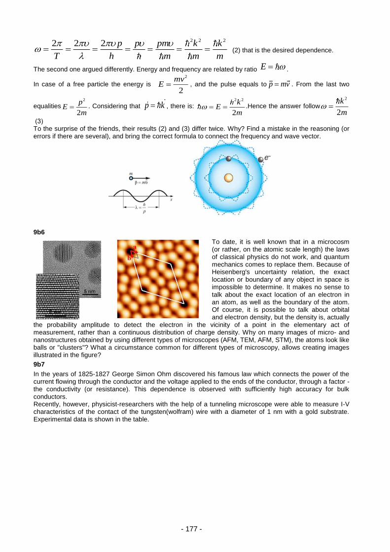
- 177 -
2 2 22 2 2 p p pm k k
T h m m m
(2) that is the desired dependence.
The second one argued differently. Energy and frequency are related by ratio E .
In case of a free particle the energy is
2
2
mvE , and the pulse equals to p mv . From the last two
equalities2
2
pE
m . Considering that p k , there is:
2 2
2
kE
m .Hence the answer follow
2
2
k
m
(3) To the surprise of the friends, their results (2) and (3) differ twice. Why? Find a mistake in the reasoning (or errors if there are several), and bring the correct formula to connect the frequency and wave vector.
9b6
To date, it is well known that in a microcosm (or rather, on the atomic scale length) the laws of classical physics do not work, and quantum mechanics comes to replace them. Because of Heisenberg's uncertainty relation, the exact location or boundary of any object in space is impossible to determine. It makes no sense to talk about the exact location of an electron in an atom, as well as the boundary of the atom. Of course, it is possible to talk about orbital and electron density, but the density is, actually
the probability amplitude to detect the electron in the vicinity of a point in the elementary act of measurement, rather than a continuous distribution of charge density. Why on many images of micro- and nanostructures obtained by using different types of microscopes (AFM, TEM, AFM, STM), the atoms look like balls or "clusters"? What a circumstance common for different types of microscopy, allows creating images illustrated in the figure?
9b7
In the years of 1825-1827 George Simon Ohm discovered his famous law which connects the power of the current flowing through the conductor and the voltage applied to the ends of the conductor, through a factor - the conductivity (or resistance). This dependence is observed with sufficiently high accuracy for bulk conductors. Recently, however, physicist-researchers with the help of a tunneling microscope were able to measure I-V characteristics of the contact of the tungsten(wolfram) wire with a diameter of 1 nm with a gold substrate. Experimental data is shown in the table.

- 178 -
Table with experimental data
U, mV I, mkA U, mV I, mkA U, mV I, mkA
7.5 0.37 276 14.95 455.6 33.76
22.7 0.83 293 16.15 470.7 35.5
45.4 1.74 300.6 16.79 480.2 36.97
68 2.66 310 17.34 493.4 38.35
92.7 3.58 323.3 17.98 502.8 39.08
111.5 4.59 330.8 18.62 514.2 40.28
149.3 6.33 342.2 20 523.6 41.93
160.7 7.25 351.6 21.56 533.1 43.58
173.9 7.89 361.1 22.29 542.5 45.32
192.8 8.81 374.3 23.67 550.1 46.97
200.4 9.45 385.6 25.23 557.7 48.53
207.9 9.91 397 26.61 567.1 50.28
225 11.2 412.1 27.8 576.6 51.74
243.9 12.48 421.6 29.45 584.1 53.3
260.9 13.76 431 30.92 593.6 55.14
266.5 14.31 442.3 32.39 601.1 56.88
1. Why gold or tungsten wires are most commonly used? 2. What effect was observed by physicists? What is the difference between current-voltage
characteristics of a tungsten wire of circular section of 1 mm diameter, 1 micron, 10 nm and 1 nm and a unit length (plot all these curves on a graph and explain).
3. Plot the conductivity of the applied voltage according to point 3. Constant G0 is usually applied to the effect. What is this constant called? What is its dimension and value in the SI system? And for what is this value currently used?
9b8
Porous silicon is an aggregate of nanocrystals and pores with sizes ranging from units to hundreds of nanometers. This material is currently subject to many research laboratories around the world because of its unique structural, optical, electronic and biological properties. Porous silicon is classified in accordance with the International Union of Pure and Applied Chemistry which determines the type of porous material depending on the size of pores.
Table. Classification of porous silicon according to the size of its porous.
The existence of equilibrium free charge carriers in mesoporous silicon nanocrystals (meso-PC) was recently proved. It was found that in addition to the bands of local surface oscillations in the spectra of IR transmission of films of meso-PC, absorption of infrared radiation due to the presence of free charge carriers (FCC) is observed.
1) How can the decrease in the concentration of free charge carriers (FCC) in mesoporous silicon nanocrystals compared with bulk silicon be explained?
2) the figure shows the absorption coefficient of crystalline silicon (c-Si) and meso-PC on the
wavelength of infrared radiation. Dependencies () were determined on the basis of measured transmission spectra according to the relation
)(Tlnh)( λλα 1 , (1)
where h – thickness of meso-PC, T () - transmission (depending on T () are obtained experimentally).
Porous silicon type Porous size
Microporous (Nanoporous)
2 nm
Mesoporous 2-50 nm
Macroporous >50 nm
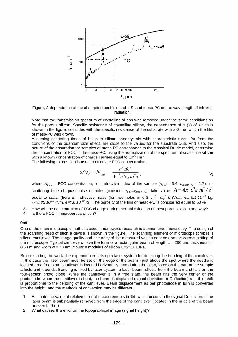
- 179 -
3 4 5 6 7 8 9 10 20
10
100
1000
ПК
c-Si
, мкм
, см
-1
Figure, A dependence of the absorption coefficient of c-Si and meso-PC on the wavelength of infrared
radiation.
Note that the transmission spectrum of crystalline silicon was removed under the same conditions as
for the porous silicon. Specific resistance of crystalline silicon, the dependence of () of which is shown in the figure, coincides with the specific resistance of the substrate with a-Si, on which the film of meso-PC was grown. Assuming scattering times of holes in silicon nanocrystals with characteristic sizes, far from the conditions of the quantum size effect, are close to the values for the substrate c-Si. And also, the nature of the absorption for samples of meso-PS corresponds to the classical Drude model, determine the concentration of FCC in the meso-PC, using the normalization of the spectrum of crystalline silicon with a known concentration of charge carriers equal to 10
20 cm
-3.
The following expression is used to calculate FCC concentration:
τεπ
λνα
*снзmc
neN)(
032
22
4 , (2)
where NFCC – FCC concentration, n – refractive index of the sample (nc-Si = 3.4, nmeso-PC = 1.7), -
scattering time of quasi-pulse of holes (consider c-Si=meso-PC), take value 2*
0
32 /4 emcA
equal to const (here m*- effective mass (for free holes in c-Si m
*= mp
*=0.37m0, m0=9.110
-31 kg;
0=8.8510-12
Ф/m, е=1.610-19
Kl). The porosity of the film of meso-PC is considered equal to 60 %.
3) How will the concentration of FCC change during thermal oxidation of mesoporous silicon and why?
4) Is there FCC in microporous silicon?
9b9
One of the main microscopic methods used in nanoworld research is atomic-force microscopy. The design of the scanning head of such a device is shown in the figure. The scanning element of microscope (probe) is silicon cantilever. The image quality and accuracy of the measured values depends on the correct setting of the microscope. Typical cantilevers have the form of a rectangular beam of length L = 200 um, thickness t = 0.5 um and width w = 40 um, Young's modulus of silicon E=2* 1010Pa.
Before starting the work, the experimenter sets up a laser system for detecting the bending of the cantilever. In this case the laser beam must be set on the edge of the beam - just above the spot where the needle is located. In a free state cantilever is located horizontally, and during the scan, force on the part of the sample affects and it bends. Bending is fixed by laser system: a laser beam reflects from the beam and falls on the four-section photo diode. While the cantilever is in a free state, the beam hits the very center of the photodiode, when the cantilever is bent, the beam is displaced (signal deviation or Deflection) and this shift is proportional to the bending of the cantilever. Beam displacement as per photodiode in turn is converted into the height, and the methods of conversion may be different.
1. Estimate the value of relative error of measurements (in%), which occurs in the signal Deflection, if the laser beam is substantially removed from the edge of the cantilever (located in the middle of the beam or even farther).
2. What causes this error on the topographical image (signal height)?
λ, μm
α,
cm
-1
PC
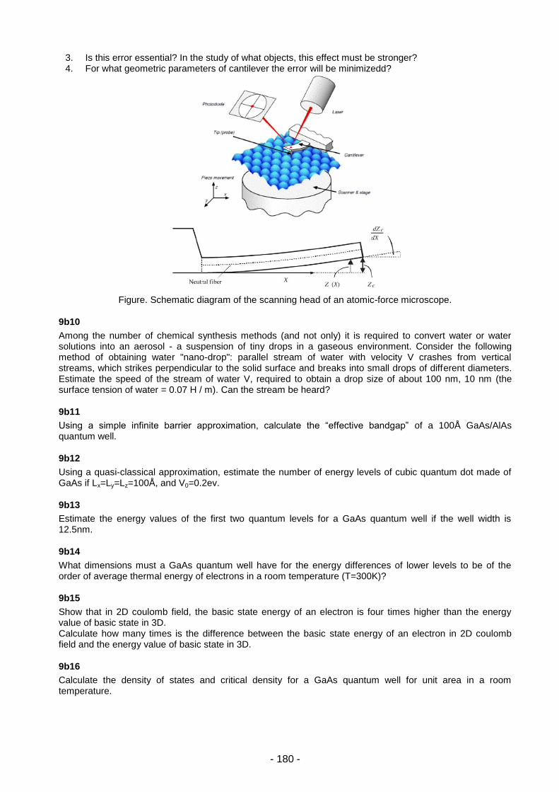
- 180 -
3. Is this error essential? In the study of what objects, this effect must be stronger? 4. For what geometric parameters of cantilever the error will be minimizedd?
Figure. Schematic diagram of the scanning head of an atomic-force microscope.
9b10
Among the number of chemical synthesis methods (and not only) it is required to convert water or water solutions into an aerosol - a suspension of tiny drops in a gaseous environment. Consider the following method of obtaining water "nano-drop": parallel stream of water with velocity V crashes from vertical streams, which strikes perpendicular to the solid surface and breaks into small drops of different diameters. Estimate the speed of the stream of water V, required to obtain a drop size of about 100 nm, 10 nm (the surface tension of water = 0.07 H / m). Can the stream be heard?
9b11
Using a simple infinite barrier approximation, calculate the “effective bandgap” of a 100Å GaAs/AlAs quantum well.
9b12
Using a quasi-classical approximation, estimate the number of energy levels of cubic quantum dot made of GaAs if Lx=Ly=Lz=100Å, and V0=0.2ev.
9b13
Estimate the energy values of the first two quantum levels for a GaAs quantum well if the well width is 12.5nm.
9b14
What dimensions must a GaAs quantum well have for the energy differences of lower levels to be of the order of average thermal energy of electrons in a room temperature (T=300K)?
9b15
Show that in 2D coulomb field, the basic state energy of an electron is four times higher than the energy value of basic state in 3D. Calculate how many times is the difference between the basic state energy of an electron in 2D coulomb field and the energy value of basic state in 3D.
9b16
Calculate the density of states and critical density for a GaAs quantum well for unit area in a room temperature.

- 181 -
9b17
Estimate the electron energy for a GaAs quantum well if the quantum well is in an electrical field for 104
V/sm.
9b18
For basic state of exciton in a GaAs/Al0.3Ga0.7As quantum well with 100Å width and 1mEv semiwidth, calculate the absorption coefficient value for a light with x polarity. Consider only the case of heavy hole. The exciton radius for a quantum well is equal to 2/3 radius of 3D case.
9b19
Draw the dependence of density of states from energy for bulk crystal, quantum well, quantum wire and quantum dot.
9b20
A GaAs/Al0.3Ga0.7As multilayer quantum structure with 100Å width has exciton (heavy hole case) absorption peak in case of 1.51eV. 80kV/sm voltage is applied to the well (exciton absorption peak change is 20meV). Calculate radiation beam intensivity ratio in case of the presence and absence of the field, if the exciton line length is 2.5eV, the total length of heterostructure is 1um, and the photon energy is 1.49eV.

- 182 -

- 183 -
ANSWERS TO TEST QUESTIONS AND
SOLUTIONS OF PROBLEMS
- 184 -
1. DIGITAL INTEGRATED CIRCUITS
a) Test questions 1a1. B 1a2. D 1a3. E 1a4. B 1a5. A 1a6. C 1a7. B 1a8. B 1a9. D 1a10. A 1a11. A 1a12. D 1a13. C 1a14. B 1a15. E 1a16. A 1a17. C 1a18. E 1a19. A 1a20. C 1a21. D 1a22. B 1a23. D 1a24. E 1a25. E 1a26. B 1a27. B 1a28. B 1a29. E 1a30. C 1a31. D 1a32. B 1a33. D 1a34. D 1a35. C 1a36. D 1a37. C 1a38. C 1a39. A 1a40. D 1a41. A 1a42. D 1a43. D 1a44 B 1a45 E 1a46 E
1a47 B 1a48. C 1a49. B 1a50. E 1a51. A 1a52. C 1a53. C 1a54. E 1a55. B 1a56. B 1a57. D 1a58. C 1a59. C 1a60. C 1a61. B 1a62. D 1a63. C 1a64. D 1a65. C 1a66. B 1a67. B 1a68. B 1a69. C 1a70. D 1a71. A 1a72. B 1a73. D 1a74. B 1a75. A 1a76. A 1a77. B 1a78. C 1a79. B 1a80. C 1a81 B 1a82. B 1a83. D 1a84. C 1a85. B 1a86. D 1a87. D 1a88. A 1a89. B 1a90. D 1a91. C 1a92. D
1a93. B 1a94. C 1a95. A 1a96. B 1a97. B 1a98. A 1a99. C 1a100. B 1a101. E 1a102. E 1a103. B 1a104. C 1a105. D 1a106. B 1a107. D 1a108. B 1a109. D 1a110. A 1a111. A 1a112. D 1a113. A 1a114. B 1a115. C 1a116. A 1a117. B 1a118. A 1a119. D 1a120. B 1a121. D 1a122. B 1a123. D 1a124. A 1a125. C 1a126. A 1a127. D 1a128. B 1a129. B 1a130. D 1a131. C 1a132. C 1a133. B 1a134. B 1a135. A 1a136. C 1a137. B 1a138. B
1a139. A 1a140. B 1a141. A 1a142. C 1a143. A 1a144. C 1a145. B 1a146. B 1a147. C 1a148. B 1a149. B 1a150. C 1a151. C 1a152. D 1a153. A 1a154. B 1a155. C 1a156. A 1a157. B 1a158. C 1a159. D 1a160. B 1a161. B 1a162. D 1a163. C 1a164. B 1a165. B 1a166. C 1a167. C 1a168. A 1a169. C 1a170. C 1a171. D 1a172. C 1a173. B 1a174. B 1a175. A 1a176. E 1a177. D 1a178. C 1a179. B 1a180. A
- 185 -
b) Problems 1b1. tsuX=tbf+tnor+tsu-tclkbf=2+7+4-3=11 ns thdX=tclkbf+thd-tbf-tnor=3+5-2-7=-1 ns tL=tclkbf+tCQ+tor=3+6+8=17 ns tcycle=tCQ+tnor+tsu=6+7+4=17 ns 1b2. 1b3.
1b4.
FSM
D Q D Q
D Q
CLK
pulse_in
reset
pulse_out
- 186 -
1b5. 1b6. D Flip Flop with High Active Set, v.1
D Flip Flop with High Active Set, v.2 1b7. D Flip Flop with High Active Set and Reset, v.1
A
B C
B
D
B D
A C
B
Z
VDD
VSS
D
SET
CLK
Q
QN
D
SET
CLK
Q
QN
D
SE
T
CL
K
Q
QN RESET
- 187 -
D Flip Flop with High Active Set and Reset, v.2
1b8.
Z=A&B+!C&B+!A&!B&C=!(!B(A+!C)+!A&B&C)
1b9.
p
n
THPTHNp
n
SP
VVDDV
V
β
β
β
β
1
, L
Wkpβ
p
n
THPTHNp
n
p
p
n
n
THPTHN
p
p
n
n
SP
W
W
kpp
kpn
VVDDVW
W
kpp
kpn
L
W
L
W
kpp
kpn
VVDDV
L
W
L
W
kpp
kpn
V
1
1
A B C Z !Z
0 0 0 0 1
0 0 1 1 0
0 1 0 1 0
0 1 1 0 1
1 0 0 0 1
1 0 1 0 1
1 1 0 1 0
1 1 1 1 0
!B
A !C
!A
C
B C
!B A
!C
Z
VDD
VSS
B
!A
D
RESET
CL
K
Q
QN SET
- 188 -
p
n
p
n
p
n
p
n
p
n
W
W
.
W
W
.W
W.
W
W
kpp
kpn
..W
W
kpp
kpn
3
11
84
3
11
84603
1
1
80560
1. Wn=3 um
643
10
3
3
11
843 .
.VSP
V
2. Wn=12 um
933
10
12
3
11
8412 .
.VSP
V
VSP12 < VSP3
12
10
n
p
W
W
3
10
n
p
W
W
Therefore, the inverter corresponds to the left curve for which Wn=12 um. 1b10. For both circuits the best case delay is the delay from input C to output Y. For the shown NAND cell the delay from A input to Y output is smaller than from B input. Therefore, the best case delay of the 2
nd circuit is smaller.
1b11.
The frequency of the ring oscillator is defined by PLHnPHLnPLHPHLPLHPHL tt...tttt
f
2211
1,
where tPHLi and tPLHi are the delays of i-th inverter’s output and fall accordingly. The number of inverters in a ring oscillator must be odd, so the 1
st and the 2
nd circuits are not included in the
ring oscillator (in operation, logic “1” is given to set input and the output NAND cell operates as an inverter). The delay from “a” input to the output of the used NAND cell is smaller than the delay from “b” input to the output, so the 4
th ring oscillator is the fastest.
1b12. a. In order to get the signal from I12 in Q and QN, it is necessary to have the correct logic state in I22 and
I23 feedback until CK fall transition. To say it otherwise, it is necessary to keep CK constant until the signal “passes” I3-I17-I23-I22 path. The signal level in I22 and I23 cells’ outputs must be either 0.9 VDD or 0.1 VDD (VDD is supply voltage). Thus, CK mustn’t switch at max(tPHLI3+tPLHI17, tPLHI3+tPHLI17)+max(triseI23+tfallI22,tfallI23+triseI22)=1650 ps.
b. As explained in item a., in this case D also must remain constant at max(tPHLI1+tPLHI11, tPLHI1+tPHLI11)+max(triseI13+tfallI12, tfallI13+triseI12)- tPLHI12=1250 ps.
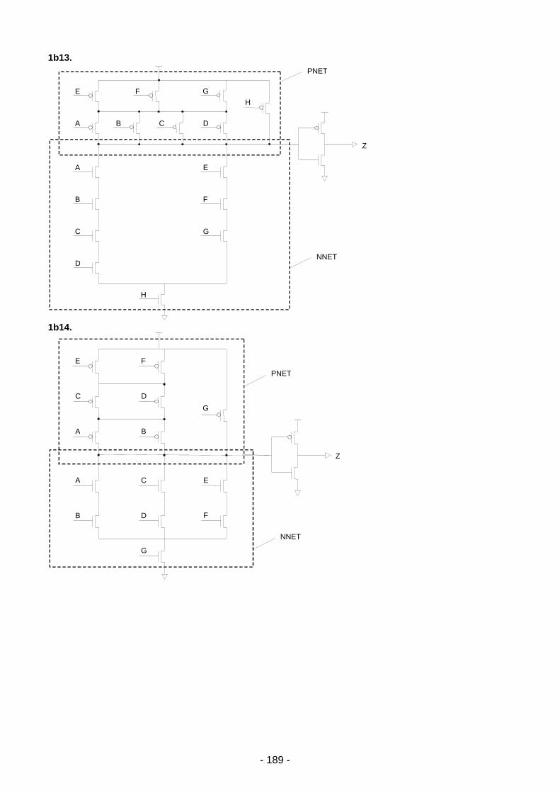
- 189 -
1b13.
1b14.
C
A
A
B
B
D G
E
F
Z
G
PNET
NNET
C
D
E F
E
A
A
B
C
D
B C D
F G H
E
F
G
Z
H
PNET
NNET
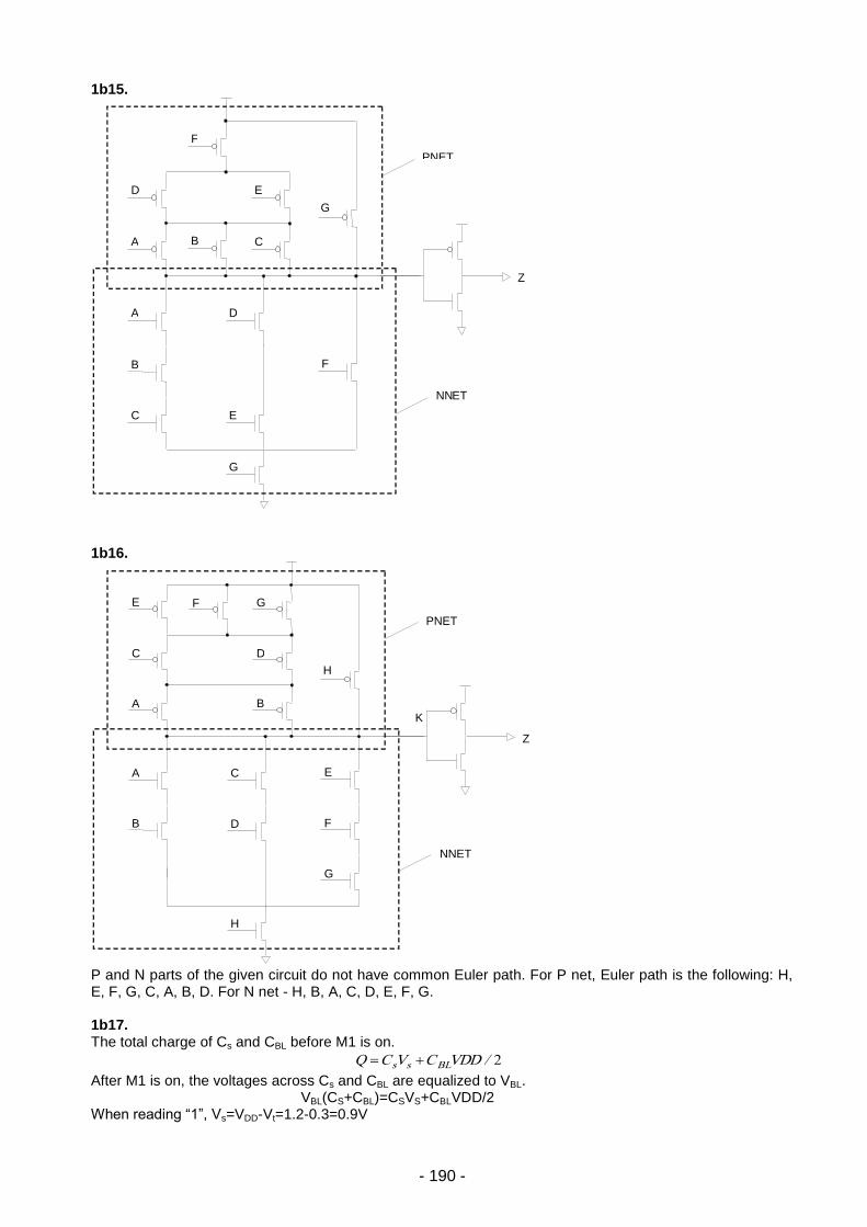
- 190 -
1b15.
1b16.
P and N parts of the given circuit do not have common Euler path. For P net, Euler path is the following: H, E, F, G, C, A, B, D. For N net - H, B, A, C, D, E, F, G. 1b17. The total charge of Cs and CBL before M1 is on.
2/VDDCVCQ BLss
After M1 is on, the voltages across Cs and CBL are equalized to VBL. VBL(CS+CBL)=CSVS+CBLVDD/2
When reading “1”, Vs=VDD-Vt=1.2-0.3=0.9V
C
A
A
B
B
D H
Z
H
PNET
NNET
C
F
F D
E
G
K
E G
D
A
A
B
C
E G
F
Z
G
PNET
NN ET
D
F
C E
B

- 191 -
BLs
BLssBL
CC
/VDDCVCV
2=(0.9Cs+0.6*10Cs)/(Cs+10Cs)=6.9/11=0.63V
When reading “0”, Vs=0 VBL=0.6*10Cs/11Cs=0.55V
1b18.
R=2VDDL/Wk (VDD-Vt)2; R1=22.50.25/41154=0.68 kOhm
R2=22.50.25/0.5302.12=19 kOhm
a) VOH=VDD=2.5V, VOL=R1/(R1+R2)=0.68/(0.68+19)2.5=0.87 mV b) 1. Vin=Low, In=0, Pdiss=0,
2. Vin=High=2.5V, In=Ip=(W/L)pkp(VDD-|Vtp|)2/2=133.2 A. Pstatic=VDDIp=2.5*133.2=333W.
c)
tpLH=0.7RpCL=0.7*19*1=13.3 ns; tpHL=0.7RnCL=0.7*0.68*1=0.476 ns 1b19. a) Y=!(CD(A+B))
NMOS (W/L)A=(W/L)B=(W/L)C/2=(W/L)D/2; (W/L)C=(W/L)D=4*3=12; (W/L)A=(W/L)B=6 PMOS (W/L)A=(W/L)B=2(W/L)C=2(W/L)D ; (W/L)C=(W/L)D=8/3; (W/L)A=(W/L)B=16/3
b) tpHL: ABCD=1010 -> 1011 or 1010 -> 0111; transistor discharges the caps in all nodes of the pull-down network, before transition all caps are charged. If D were on before transition then D’s drain node cap would be discharged, so tpHL would be less. tpLH: ABCD=1111 -> 0011; before transition all caps are charged, AB path discharges these caps.
1b20.
P(Y=1)=(1-P(A=1)P(C=1)P(D=1)) (1-P(B=1)P(C=1)P(D=1))= =(1-0.5*0.3*0.8)(1-0.2*0.3*0.8)=0.88*0.952=0.83776
P(Y=0)=1- P(Y=1)=1-0.83776=0.16224 P0-1=P1-0= P(Y=0)*P(Y=1)= 0.1359181824=0.136
αsw= P0-1
Psw= αsw VDD2FclkCout=0.136*2.5
2*250*10
6*30*10
-15=0.659*10
-5W=6.59W
1b21. Verilog Description module counter_rev(clk,ce,clr,load,d,up,q,tc);
input clk, ce, clr,load,up;
input[7:0] d;
output tc;
reg tc;
output[7:0] q;
reg[7:0] q;
always @(posedge clk or posedge clr)
begin
if(clr==1) q<=8'b0;
else if(load) q<=d;
else if (ce==0)
q<=q;
else if (up==1)
q<=q+1;
else q<=q-1;
end
always @(q or up)
begin if((q==8'd255)&&(up==1))
tc=1;
else if((q==8'b0)&&(up==0))
tc=1;
else tc=0; end
endmodule
Constructing a counter circuit diagram based on T Flip-Flop To construct a circuit diagram use T flip-flops with asynchronous reset, synchronous loading and enable input.
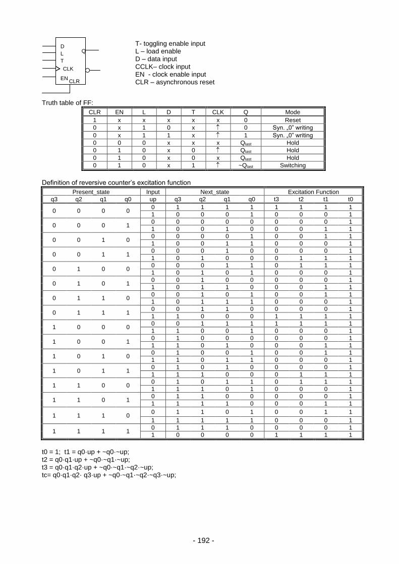
- 192 -
Truth table of FF:
CLR EN L D T CLK Q Mode
1 x x x x x 0 Reset
0 x 1 0 x 0 Syn. „0” writing
0 x 1 1 x 1 Syn. „0” writing
0 0 0 x x x Qlast Hold
0 1 0 x 0 Qlast Hold
0 1 0 x 0 x Qlast Hold
0 1 0 x 1 ~Qlast Switching
Definition of reversive counter’s excitation function
Present_state Input Next_state Excitation Function
q3 q2 q1 q0 up q3 q2 q1 q0 t3 t2 t1 t0
0 0 0 0 0 1 1 1 1 1 1 1 1
1 0 0 0 1 0 0 0 1
0 0 0 1 0 0 0 0 0 0 0 0 1
1 0 0 1 0 0 0 1 1
0 0 1 0 0 0 0 0 1 0 0 1 1
1 0 0 1 1 0 0 0 1
0 0 1 1 0 0 0 1 0 0 0 0 1
1 0 1 0 0 0 1 1 1
0 1 0 0 0 0 0 1 1 0 1 1 1
1 0 1 0 1 0 0 0 1
0 1 0 1 0 0 1 0 0 0 0 0 1
1 0 1 1 0 0 0 1 1
0 1 1 0 0 0 1 0 1 0 0 1 1
1 0 1 1 1 0 0 0 1
0 1 1 1 0 0 1 1 0 0 0 0 1
1 1 0 0 0 1 1 1 1
1 0 0 0 0 0 1 1 1 1 1 1 1
1 1 0 0 1 0 0 0 1
1 0 0 1 0 1 0 0 0 0 0 0 1
1 1 0 1 0 0 0 1 1
1 0 1 0 0 1 0 0 1 0 0 1 1
1 1 0 1 1 0 0 0 1
1 0 1 1 0 1 0 1 0 0 0 0 1
1 1 1 0 0 0 1 1 1
1 1 0 0 0 1 0 1 1 0 1 1 1
1 1 1 0 1 0 0 0 1
1 1 0 1 0 1 1 0 0 0 0 0 1
1 1 1 1 0 0 0 1 1
1 1 1 0 0 1 1 0 1 0 0 1 1
1 1 1 1 1 0 0 0 1
1 1 1 1 0 1 1 1 0 0 0 0 1
1 0 0 0 0 1 1 1 1
t0 = 1; t1 = q0·up + ~q0·~up; t2 = q0·q1·up + ~q0·~q1·~up; t3 = q0·q1·q2·up + ~q0·~q1·~q2·~up; tc= q0·q1·q2· q3·up + ~q0·~q1·~q2·~q3·~up;
D
L
T
CLK
Q
CLR EN
T- toggling enable input L – load enable D – data input CCLK– clock input EN - clock enable input CLR – asynchronous reset
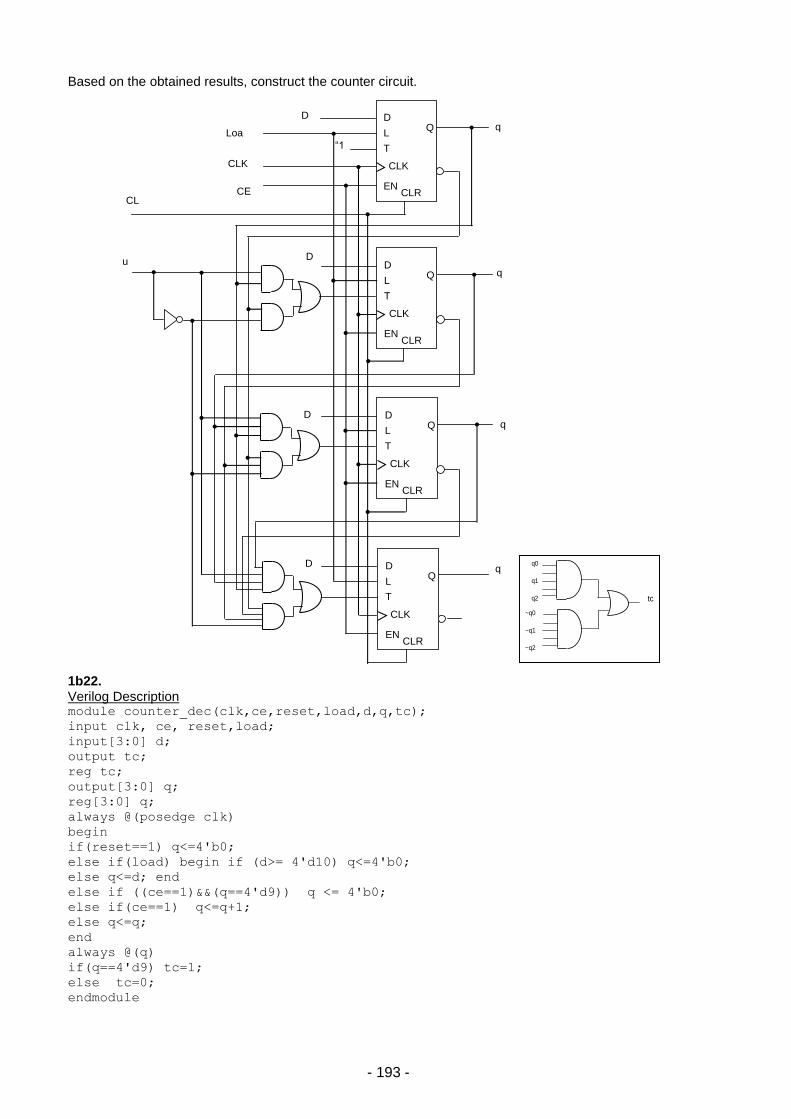
- 193 -
Based on the obtained results, construct the counter circuit.
1b22. Verilog Description module counter_dec(clk,ce,reset,load,d,q,tc);
input clk, ce, reset,load;
input[3:0] d;
output tc;
reg tc;
output[3:0] q;
reg[3:0] q;
always @(posedge clk)
begin
if(reset==1) q<=4'b0;
else if(load) begin if (d>= 4'd10) q<=4'b0;
else q<=d; end
else if ((ce==1)&&(q==4'd9)) q <= 4'b0;
else if(ce==1) q<=q+1;
else q<=q;
end
always @(q)
if(q==4'd9) tc=1;
else tc=0;
endmodule
D
L
T
CLK
Q
CLR EN
D
L
T
CLK
Q
CLR EN
D
L
T
CLK
Q
CLR EN
D
L
T
CLK
Q
CLR EN
q
0
q
1
u
p
q
2
CL
R
D
0
D
1
D
2
D
3
“1
”
Loa
d
CE
CLK
q
3
q0
q1
q2
q3
up
~q0
~q1
~q2
~q3
tc
- 194 -
Constructing a counter circuit diagram based on T Flip-Flop To construct a circuit diagram use T flip-flops with asynchronous reset, synchronous loading and enable input.
Truth table of FF:
CLR EN L D T CLK Q Mode
1 x x x x 0 Reset
1 x 1 0 x 0 Syn. „0” writing
1 x 1 1 x 1 Syn. „0” writing
1 0 0 x x x Qlast Hold
1 1 0 x 0 Qlast Hold
1 1 0 x 0 x Qlast Hold
1 1 0 x 1 ~Qlast Switching
Definition of binary-coded decimal counter’s excitation function:
q3 q2 q1 q0 t3 t2 t1 t0
0 0 0 0 0 0 0 1
0 0 0 1 0 0 0 1
0 0 1 0 0 0 1 1
0 0 1 1 0 1 1 1
0 1 0 0 0 0 0 1
0 1 0 1 0 0 1 1
0 1 1 0 0 0 0 1
0 1 1 1 1 1 1 1
1 0 0 0 0 0 0 1
1 0 0 1 1 0 0 1
Exitation Function’s Minimization using Karnaugh Maps
t0 = 1 t1 = q0·q3+~q0·q3 t2 = q0·q1 t3 = q0·q3
00
01
11
10
00 01 11 10 q3q2
q1q0
00
01
11
10
00 01 11 10 q3q2
q1q0
00
01
11
10
00 01 11 10 q3q2
q1q0
t0 = 1 t1 = q0·q3+~q0·q2 t2 = q0·q1 t3 = q0·q3
t3 t2
t1
1
1
1
1
1 1
1 1
D
L
T
CLK
Q
CLR EN
T- toggling enable input L – load enable D – data input CLK– clock input EN - clock enable input CLR – synchronous reset
- 195 -
Circuit diagram is constructed based on the obtained results.
1b23. Creation of State Transition Graph of FSM The digits of entering decimal number are given on the entries of FSM sequentially.The remainder of division of a decimal number by 3 is equal to the remainder of division of the sum of decimal digits of this number by 3. FSM is given by means of the following five sets: А = { X, Y,
S, , }, where: Х = {X1, X2 . . . XM} – set of input symbols; Y = {Y1, Y2 . . . YN} – set of output symbols; S = {S0, S1 . . . SK-1} – set of internal states of FSM;
– next state (transition) function,
- output function.
The considered FSM has 3 states S = {S0,S1,S2}, where, S0 – the remainder equal to 0,S1 – the remainder equal to 1,S2 – the remainder equal to 2. X = {0,1,2,3,4,5,6,7,8,9} Y = {0,1,2} S = {S0,S1,S2}
D
L
T
CLK
Q
CLR EN
D
L
T
CLK
Q
CLR EN
D
L
T
CLK
Q
CLR EN
D
L
T
CLK
Q
CLR EN
q0
q1
q2
CLR
D0
D1
D2
D3
“1”
Load
CE
CLK
q3
tc
0369
0369
147
0369
258 S1/1
S0/0
S2/2
147
258
147 147

- 196 -
Verilog Description of FSM module fsm_remainder(in,clk,reset,out);
input[3:0] in;
input clk, reset;
output[1:0] out;
reg [1:0] out;
reg[1:0] state, next_state;
parameter S0=2'b00, S1=2'b01, S2=2'b10;
always @(posedge clk or negedge reset)
if(!reset) state <= S0;
else state<=next_state;
always @(in or state)
begin
case(state)
S0: case(in)
4'd0,4’d3,4’d6,4’d9: next_state=S0;
4'd1, 4’d4, 4’d7: next_state=S1;
4'd2, 4’d5, 4’d8: next_state=S2;
default: next_state=S0;
endcase
S1: case(in)
4'd0,4’d3,4’d6,4’d9: next_state=S1;
4'd1, 4’d4, 4’d7: next_state=S2;
4'd2, 4’d5, 4’d8: next_state=S0;
default: next_state=S0;
endcase
S2: case(in)
4'd0,4’d3,4’d6,4’d9: next_state=S2;
4'd1, 4’d4, 4’d7: next_state=S0;
4'd2, 4’d5, 4’d8: next_state=S1;
default: next_state=S0;
endcase
default: next_state=S0;
endcase
end
always @(state)
if(state==S0) out=2'b00;
else if (state==S1) out = 2'b01;
else if (state ==S2) out = 2'b10;
else out=2'bxx;
endmodule
Synthesis of FSM Using JK Flip-Flops 1. Definition of input and output signals
To code decimal digits n = log210 = 4 input variables are required, as x3, x2, x1, x0. Binary-coded decimal digits: Y = {0, 1, 2}.
Decimal digit x3 x2 x1 x0
“0” 0 0 0 0
“1” 0 0 0 1
“2” 0 0 1 0
“3” 0 0 1 1
“4” 0 1 0 0
“5” 0 1 0 1
“6” 0 1 1 0
“7” 0 1 1 1
“8” 1 0 0 0
“9” 1 0 0 1
To code output signals two variables are required, as y1, y0.
Output y1 y0
“0” 0 0
“1” 0 1
“2” 1 0

- 197 -
So, FSM has 4 inputs and 2 outputs. 2. State assignment The number of required state variables k is defined as follows:
23. Accept k=2. S0 – 00 S1 – 01 S2 – 10 Unused state – 00 (solution of minimal-value) Definition of excitation function
Transition J K
0 - 0 0 x
0 - 1 1 x
1 - 0 x 1
1 - 1 x 0
State and output table
Present_state Output Input Next_State Excitation Functions
q1 q0 y1 y0 X q1 q0 j1 k1 j0 k0
0 0
0 0
0v3v6í9 0 0 0 - 0 -
1í4í7 0 1 0 - 1 -
1 0 1 - 0 -
0 1
0 1
0v3v6v9 0 1 0 - - 0
1v4v7 1 0 1 - - 1
2v5v8 0 0 0 - - 1
1 0
1 0
0v3v6v9 1 0 - 0 0 -
1v4v7 0 0 - 1 0 -
2v5v8 0 1 - 1 1 -
Excitation functions depend on 6 variables: q1,q2,x0,x1,x2,x3. Тo simplify the process of designing w1, w2, w3 extra variables are inserted: 0v3v6v9 - w1; 1v4v7 - w2; 2v5v8 - w3; Karnaugh maps for w1,w2,w3.
Definition of j1,k1,j2,k2 excitation functions as function of w1,w2,w3,q1,q0. j1=w1f1 +w2f2+w3f3; k1=w1g1+w2g2+w3g3 j0=w1p1+w2p2+w3p3, k0=w1t1+w2t2+w3t3, where f1…f3,g1,…g3, p1…p3, t1... t3 depend on q1,q2 variables.
00
01
11
10
00 01 11 10 x3x2
x1x0 w1
x3
x2
x0
1 1
1
1
- - - -
- -
00
01
11
10
00 01 11 10 x3x2
x1x0 w2
x0
- - - -
- -
1
1
1
x3
x2
00
01
11
10
00 01 11 10 x3x2
x1x0 w3
x0
- - - -
- -
1
1
1 x3
x2
x1
w1 = ~x3·~x2·~x1·~x0 + ~x2·x1·x0 + x2·x1·~x0 + x3·x0 w2 = ~x3·~x2·~x1·x0 + x2·~x1·~x0 +x2·x1·x0 w3 = x3·~x0 + x2·~x1·x0 + ~x2·x1·x0
- 198 -
As follows from the above table, f1 and g1 are equal to 0. So, j1=w2q2 + w3~q2; k1 = w2 + w3; j0=w2~q1+ w3q1; k0=w2 + w3; y1=q1; y0=q0;
FSM circuit diagram
y1
y0
J
CLK
CLR K
J
CLK
CLR K
q1
q0
x3
x2
x1
x0
~x3 ~x2 ~x1 x0
x2 ~x1 ~x0
x2 x1 x0
x2 ~x1 x0
~x2 x1 x0
x3 ~x0
clk
clr
q1
q0
0
1
1 0 q1
q0
0
1
1 0 q1
q0
0
1
1 0 q1
q0
0
1
1 0
j1 k1 J0 K0
0 1
- - - - - 1
- - 1 - - 1
- 0
f2 = q2 g2=1 p2=1
t2=1
Maps for definition f2,g2,p2,t2 (factors for w2)
q1
q0
0
1
1 0 q1
q0
0
1
1 0 q1
q0
0
1
1 0 q1
q0
0
1
1 0
J1 k1 J0
- - - -
1 - - 0 - - 1 0
- 1 1 -
K0
f3=~q2
g3=1 p3=q1 t3=1
Maps for definition f3,g3,p3,t3 (factors for w3)
q1
q0
0
1
1 0 q1
q0
0
1
1 0
1 -
1
-
0 0 0
0
Maps for defining y1, y0
- 199 -
1b24. Creation of State Transition Graph of FSM FSM is given by means of the following five sets: А =
{ X, Y, S, , }, where Х = {X1, X2 . . . XM} – set of input symbols; Y = {Y1, Y2 . . . YN} – set of output symbols; S = {S0, S1 . . . SK-1} – set of internal states of FSM;
– next state (transition) function,
- output function X={00,01,10,11} Y={0,1}
S0 – got zero 1s (modulo 5) S1 – got one 1 (modulo 5) S2 – got two 1s (modulo 5) S3 – got three 1s (modulo 5) S4 – got four 1s (modulo 5)
Verilog Description of FSM module moore_countmod5(data,clock,reset,out);
input reset, clock;
input[1:0] data;
output out;
reg out;
reg [2:0] state, next_state;
parameter st0 = 3'b000, st1 = 3'b001, st2 = 3'b010, st3=3'b011, st4=3'b100;
//FSM register
always @(posedge clock or negedge reset)
begin: statereg
if(!reset) //asynchronous reset
state <= st0;
else state <= next_state;
end //statereg
//FSM next_state logic
always @(state or data)
begin: fsm
case (state)
st0: case (data)
2'b00: next_state = st0;
2’b01,2’b10: next_state = st1;
2’b11: next-state = st2;
default: next_state = st0;
endcase
st1:case(data)
2'b00: next_state =st1;
2’b01, 2’b10: next_state=st2;
2'b11: next_state = st3;
default: next_state = st0;
endcase
st2: case(data)
2'b00: next_state = st2;
2’b01, 2’b10: next_state=st3;
2'b11: next_state = st4;
default: next_state = st0;
endcase
st3: case(data)
2'b00: next_state = st3;
2’b01, 2’b10: next_state=st4;
2'b11: next_state = st0;
default: next_state = st0;
endcase
st4: case(data)
2'b00: next_state = st4;
2’b01, 2’b10: next_state=st0;
2'b11: next_state = st1;
default: next_state = st0;
endcase
S0/1
S1/0
S2/0
00 00
00
S4/0 00
S3/0 00
0110
11
0110
0110
11
0110
11
11
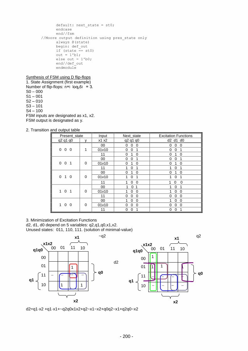
- 200 -
default: next_state = st0;
endcase
end//fsm
//Moore output definition using pres_state only
always @(state)
begin: def_out
if (state == st0)
out = 1'b1;
else out = 1'b0;
end//def_out
endmodule
Synthesis of FSM using D flip-flops 1. State Assignment (first example) Number of flip-flops: 2 . S0 – 000 S1 – 001 S2 – 010 S3 – 101 S4 – 100 FSM inputs are designated as x1, x2. FSM output is designated as y. 2. Transition and output table
Present_state Input Next_state Excitation Functions
q2 q1 q0 y x1 x2 q2 q1 q0 d2 d1 d0
0 0 0
1
00 0 0 0 0 0 0
01v10 0 0 1 0 0 1
11 0 1 0 0 1 0
0 0 1
0
00 0 0 1 0 0 1
01v10 0 1 0 0 1 0
11 1 0 1 1 0 1
0 1 0
0
00 0 1 0 0 1 0
01v10 1 0 1 1 0 1
11 1 0 0 1 0 0
1 0 1
0
00 1 0 1 1 0 1
01v10 1 0 0 1 0 0
11 0 0 0 0 0 0
1 0 0
0
00 1 0 0 1 0 0
01v10 0 0 0 0 0 0
11 0 0 1 0 0 1
3. Minimization of Excitation Functions d2, d1, d0 depend on 5 variables: q2,q1,q0,x1,x2. Unused states: 011, 110, 111. (solution of minimal-value)
d2=q1·x2 +q1·x1+~q2q0x1x2+q2~x1~x2+q0q2~x1+q2q0~x2
00
01
11
10
00 01 11 10 q1q0
x1x2
q1
q0
x1
x2
00
01
11
10
00 01 11 10 q1q0
x1x2
q1
q0
x1
x2
~q2 q2
d2
1 1
1 1
1 1
1
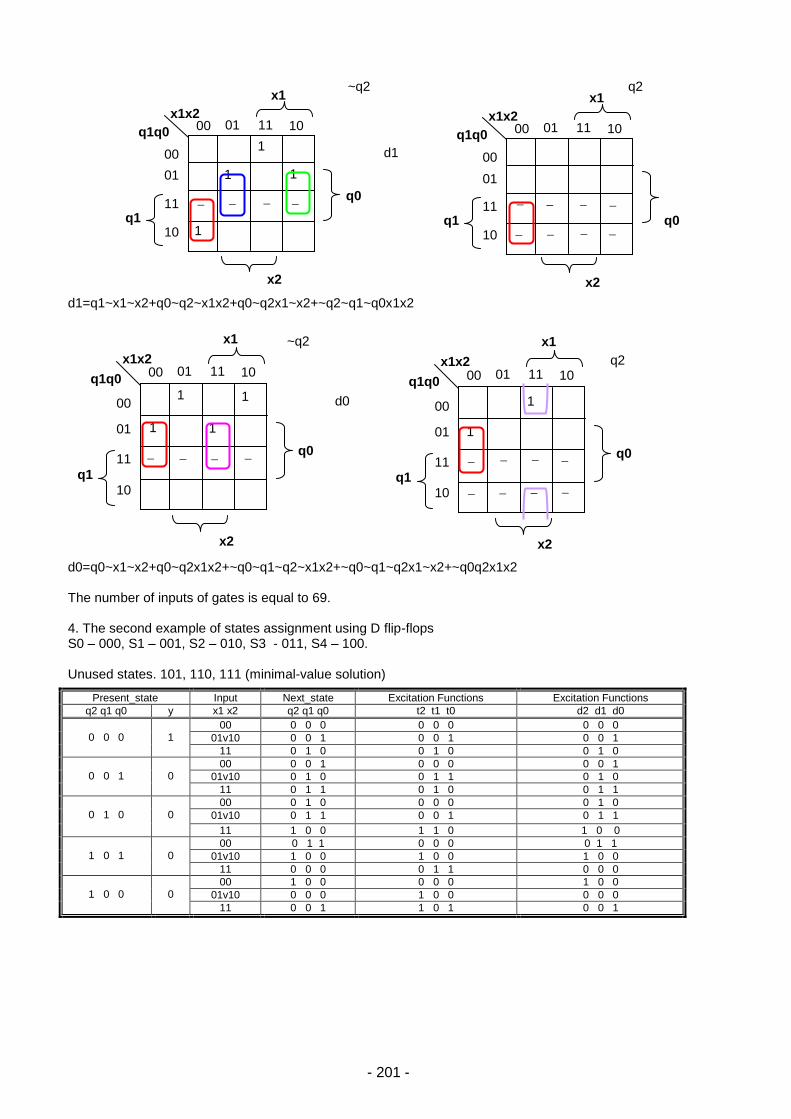
- 201 -
d1=q1~x1~x2+q0~q2~x1x2+q0~q2x1~x2+~q2~q1~q0x1x2
d0=q0~x1~x2+q0~q2x1x2+~q0~q1~q2~x1x2+~q0~q1~q2x1~x2+~q0q2x1x2 The number of inputs of gates is equal to 69. 4. The second example of states assignment using D flip-flops S0 – 000, S1 – 001, S2 – 010, S3 - 011, S4 – 100. Unused states. 101, 110, 111 (minimal-value solution)
Present_state Input Next_state Excitation Functions Excitation Functions
q2 q1 q0 y x1 x2 q2 q1 q0 t2 t1 t0 d2 d1 d0
0 0 0
1
00 0 0 0 0 0 0 0 0 0
01v10 0 0 1 0 0 1 0 0 1
11 0 1 0 0 1 0 0 1 0
0 0 1
0
00 0 0 1 0 0 0 0 0 1
01v10 0 1 0 0 1 1 0 1 0
11 0 1 1 0 1 0 0 1 1
0 1 0
0
00 0 1 0 0 0 0 0 1 0
01v10 0 1 1 0 0 1 0 1 1
11 1 0 0 1 1 0 1 0 0
1 0 1
0
00 0 1 1 0 0 0 0 1 1
01v10 1 0 0 1 0 0 1 0 0
11 0 0 0 0 1 1 0 0 0
1 0 0
0
00 1 0 0 0 0 0 1 0 0
01v10 0 0 0 1 0 0 0 0 0
11 0 0 1 1 0 1 0 0 1
00
01
11
10
00 01 11 10 q1q0
x1x2
q1
q0
x1
x2
00
01
11
10
00 01 11 10 q1q0
x1x2
q1
q0
x1
x2
~q2
q2
d0
1 1
1 1 1
1
00
01
11
10
00 01 11 10 q1q0
x1x2
q1
q0
x1
x2
00
01
11
10
00 01 11 10 q1q0
x1x2
q1 q0
x1
x2
~q2 q2
d1
1
1 1
1
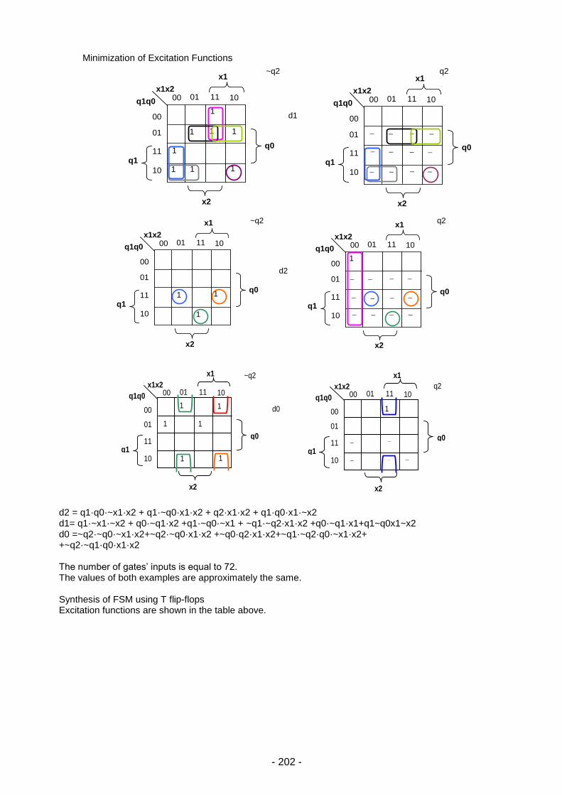
- 202 -
Minimization of Excitation Functions
d2 = q1·q0·~x1·x2 + q1·~q0·x1·x2 + q2·x1·x2 + q1·q0·x1·~x2 d1= q1·~x1·~x2 + q0·~q1·x2 +q1·~q0·~x1 + ~q1·~q2·x1·x2 +q0·~q1·x1+q1~q0x1~x2 d0 =~q2·~q0·~x1·x2+~q2·~q0·x1·x2 +~q0·q2·x1·x2+~q1·~q2·q0·~x1·x2+ +~q2·~q1·q0·x1·x2 The number of gates’ inputs is equal to 72. The values of both examples are approximately the same. Synthesis of FSM using T flip-flops Excitation functions are shown in the table above.
00
01
11
10
00 01 11 10 q1q0
x1x2
q1
q0
x1
x2
00
01
11
10
00 01 11 10 q1q0
x1x2
q1
q0
x1
x2
~q2 q2
d1
1
1
1
1 1
1 1
1
00
01
11
10
00 01 11 10 q1q0
x1x2
q1
q0
x1
x2
00
01
11
10
00 01 11 10 q1q0
x1x2
q1
q0
x1
x2
~q2 q2
d2
1
1 1
1
00
01
11
10
00 01 11 10 q1q0
x1x2
q1
q0
x1
x2
00
01
11
10
00 01 11 10 q1q0
x1x2
q1
q0
x1
x2
~q2
q2
d0
1 1
1 1
1
1 1
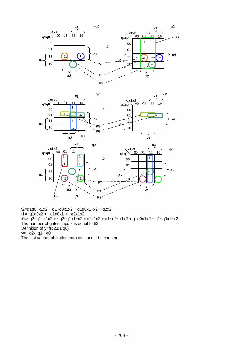
- 203 -
t2=q1q0~x1x2 + q1~q0x1x2 + q1q0x1~x2 + q2x2; t1=~q1q0x2 + ~q1q0x1 + ~q2x1x2 t0=~q2~q1~x1x2 + ~q2~q1x1~x2 + q2x1x2 + q1~q0~x1x2 + q1q0x1x2 + q1~q0x1~x2 The number of gates’ inputs is equal to 63. Definition of y=f(q2,q1,q0) y= ~q2·~q1·~q0 The last variant of implementation should be chosen.
00
01
11
10
00 01 11 10 q1q0
x1x2
q1
q0
x1
x2
00
01
11
10
00 01 11 10 q1q0
x1x2
q1
q0
x1
x2
~q2
q2
t0
1 1
1 1
1 1
1
1
P7
P8
P9 P10
P11
00
01
11
10
00 01 11 10 q1q0
x1x2
q1
q0
x1
x2
00
01
11
10
00 01 11 10 q1q0
x1x2
q1
q0
x1
x2
~q2 q2
t1
1
1 1
1
1
1
P5
P6
P7
00
01
11
10
00 01 11 10 q1q0
x1x2
q1
q0
x1
x2
00
01
11
10
00 01 11 10 q1q0
x1x2
q1
q0
x1
x2
~q2 q2
t2
P1
1
1 1
1 1
P2
P3
P4
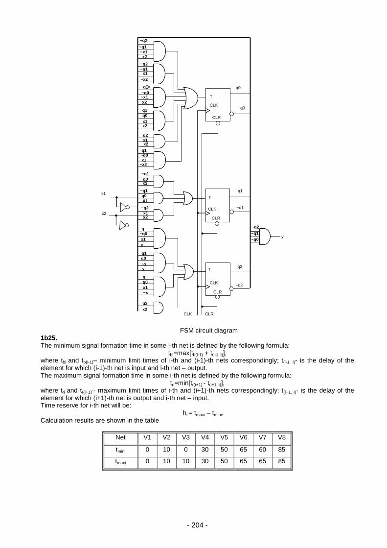
- 204 -
FSM circuit diagram
1b25. The minimum signal formation time in some i-th net is defined by the following formula:
tbi=max[tb(i-1) + t(i-1, i)], where tbi and tb(i-1)– minimum limit times of i-th and (i-1)-th nets correspondingly; t(i-1, i)- is the delay of the element for which (i-1)-th net is input and i-th net – output. The maximum signal formation time in some i-th net is defined by the following formula:
tri=min[tr(i+1) - t(i+1, i)], where tri and tr(i+1)– maximum limit times of i-th and (i+1)-th nets correspondingly; t(i+1, i)- is the delay of the element for which (i+1)-th net is output and i-th net – input. Time reserve for i-th net will be:
hi = tmaxi – tmini. Calculation results are shown in the table
Net V1 V2 V3 V4 V5 V6 V7 V8
tmini 0 10 0 30 50 65 60 85
tmaxi 0 10 10 30 50 65 65 85
x1
x2
q0
~q0
q1
~q1
~q2
q2
~q2
~q1
~x1 x2
~q2
~q1 ~q1
x1
~x2
q1
~q0 ~x1
x2
q1
q0
x1 x2
q2 x1 x2
q1 ~q0 x1
~x2
~q1
q0 x2
X1
q0 ~q1
~q2
x1 x2
q
1 ~q0
x1
x
2
q0
~x
1 x
2
q1
q
1 q0
x1
~x
2
q2
x2
T
CLK
CLK
T
T
CLK
CLR
CLR
CLR
~q2
~q1
~q0 y
CLK CLR

- 205 -
Critical path passes through all the nets for which tbi=tri, i.e. V1, V2, V4, V5, V6, V8. The total delay of that path is 85.
1b26. The equivalent circuit of interconnect’s 3-segment, R,C distributed parameters will look like this:
The delay in it will be
= rc + 2rc + 3rc = 6rc: r =[(300:3):0,2]x0,1 = 50 Ohm,
10103
300 .c fF
c = (300:3)x0,1 = 10 fF,
= 6x50x10 = 3000 OhmfF = 3 ns.
1b27. Present the given circuit in the view of 4 sequentially connected regions: Designate faultness probabilities of those regions
PΣ1, PΣ2, PΣ3, PΣ4. Using probability summing, multiplication and full probability laws, the following can be written:
PΣ1 = P1P1 + 2P1(1-P1)= P1(2-P1)=0,5(2-0,5)=0,75 PΣ2 = P2(2-P2)=0,84
PΣ3 = P3=0,8 PΣ4 = P4(2-P4)=0,64
The faultness probability of the circuit will be:
P= PΣ1 PΣ1 PΣ1 PΣ1=0,750,840,80,64=0,32256. 1b28. R, C equivalent circuit of interconnect will look as follows:
e2 e3
e4 e5
V2
V3
V4
V5
V6
V7
V1 e1
e6 V8
I2
I1
O1
r r r
c c c
P4
P4 P2
P2
P3
P1
P1
PΣ1 PΣ2 PΣ3 PΣ4
r r r
c c c c c
r
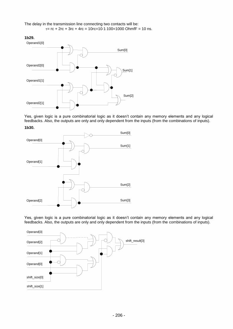
- 206 -
The delay in the transmission line connecting two contacts will be:
= rc + 2rc + 3rc + 4rc = 10rc=101100=1000 OhmfF = 10 ns. 1b29.
Yes, given logic is a pure combinatorial logic as it doesn’t contain any memory elements and any logical feedbacks. Also, the outputs are only and only dependent from the inputs (from the combinations of inputs).
1b30.
Yes, given logic is a pure combinatorial logic as it doesn’t contain any memory elements and any logical feedbacks. Also, the outputs are only and only dependent from the inputs (from the combinations of inputs).
shift_size[0]
shift_result[3]
shift_size[1]
Operand[3]
Operand[2]
Operand[1]
Operand[0]
Operand[0]
Sum[0]
Operand[1]
Sum[1]
Operand[2]
Sum[2]
Sum[3]
Operand1[0]
Operand2[0]
Sum[0]
Operand1[1]
Operand2[1]
Sum[1]
Sum[2]
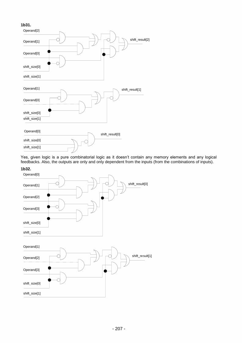
- 207 -
1b31.
Yes, given logic is a pure combinatorial logic as it doesn’t contain any memory elements and any logical feedbacks. Also, the outputs are only and only dependent from the inputs (from the combinations of inputs).
1b32.
shift_re sult[1]
shift_size[0]
shift_size[1]
Operand[1]
Operand[2]
Operand[3]
shift_size[0]
shift_result[0]
shift_size[1]
Operand[0]
Operand[1]
Operand[2]
Operand[3]
Operand[0]
shift_size[0] shift_size[1]
shift_result[0]
shift_size[0] shift_size[1]
shift_size[0]
Operand[1]
Operand[0]
shift_result[1]
shift_result[2]
shift_size[0]
shift_size[1]
Operand[2]
Operand[1]
Opera nd[0]
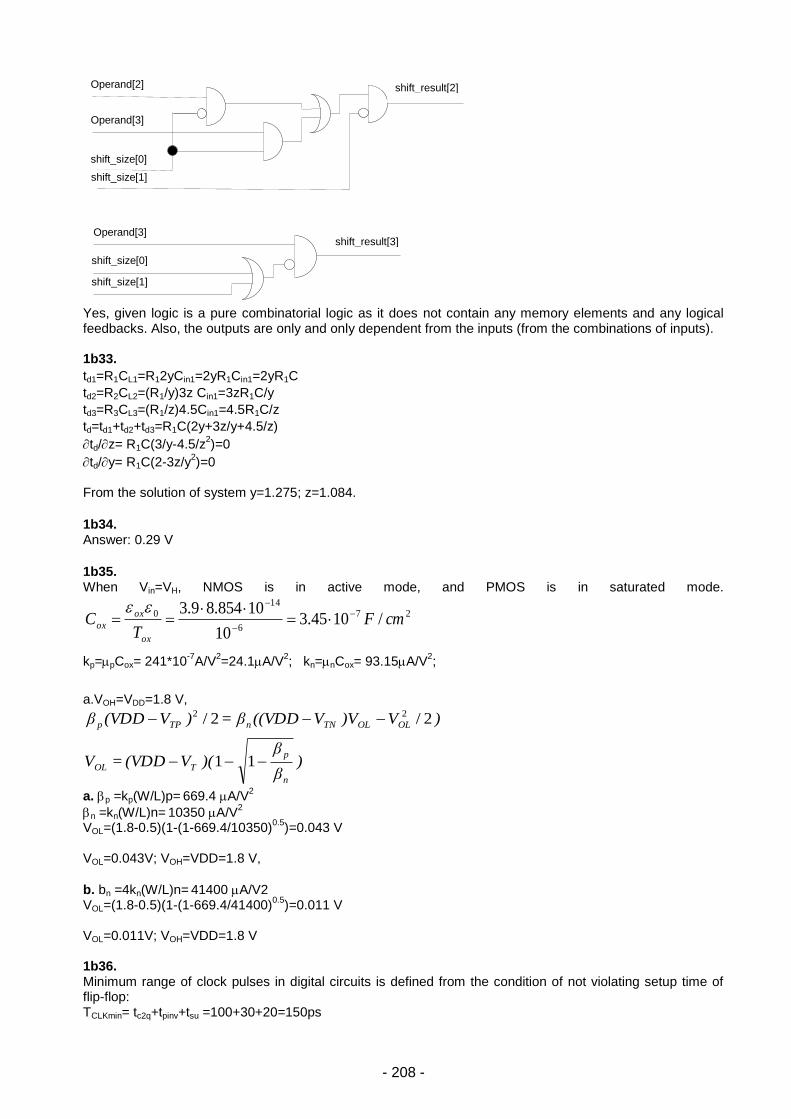
- 208 -
Yes, given logic is a pure combinatorial logic as it does not contain any memory elements and any logical feedbacks. Also, the outputs are only and only dependent from the inputs (from the combinations of inputs). 1b33.
td1=R1CL1=R12yCin1=2yR1Cin1=2yR1C
td2=R2CL2=(R1/y)3z Cin1=3zR1C/y
td3=R3CL3=(R1/z)4.5Cin1=4.5R1C/z
td=td1+td2+td3=R1C(2y+3z/y+4.5/z)
td/z= R1C(3/y-4.5/z2)=0
td/y= R1C(2-3z/y2)=0
From the solution of system y=1.275; z=1.084.
1b34. Answer: 0.29 V
1b35. When Vin=VH, NMOS is in active mode, and PMOS is in saturated mode.
27
6
140 /1045.3
10
10854.89.3cmF
TC
ox
ox
ox
kp=pCox= 241*10-7
A/V2=24.1A/V
2; kn=nCox= 93.15A/V
2;
a.VOH=VDD=1.8 V,
)β
β)(V(VDD=V
)V)VV((VDDβ=)V(VDDβ
n
p
TOL
OLOLTNnTPp
11
2/2/ 22
a. p =kp(W/L)p=
669.4 A/V
2
n =kn(W/L)n= 10350 A/V
2
VOL=(1.8-0.5)(1-(1-669.4/10350)0.5
)=0.043 V VOL=0.043V; VOH=VDD=1.8 V,
b. bn =4kn(W/L)n= 41400 A/V2
VOL=(1.8-0.5)(1-(1-669.4/41400)0.5
)=0.011 V VOL=0.011V; VOH=VDD=1.8 V 1b36. Minimum range of clock pulses in digital circuits is defined from the condition of not violating setup time of flip-flop: TCLKmin= tc2q+tpinv+tsu =100+30+20=150ps
Operand[3]
shift_size[0] shift_size[1]
shift_result[3]
shift_size[1]
shift_size[0]
Operand[2]
Operand[3]
shift_result[2]
- 209 -
1b37.
a. V625.0110060
100
A
AVV
AV
V VCC
CV
b. CVsw=CV+2CAV=60+2Ē100=260 fF 1b38. Design of Moore’s FSM:
Description of FSM by Verilog module fsm(in,out,clk,reset);
input clk,reset;
input[2:0] in;
output out;
reg out;
reg[2:0] state, next_state;
parameter s0=3'b000, s1=3'b001, s2=3'b010, s3=3'b011, s4=3'b100,s5=3'b101,s6=3'b110;
//state register
always @(posedge clk or negedge reset)
begin
if (!reset) state=s0;
else state=next_state;
end
//next state logic
always @(state or in)
begin
case (state)
s0: case (in)
3'b000: ßnext_state=state;
3'b001,3'b010,3'b100: next_state=s1;
3'b011,3'b101,3'b110: next_state=s2;
3'b111: next_state=s3;
default: next_state=s0;
endcase
s1: case (in)
3'b000: next_state=state;
3'b001,3'b010,3'b100: next_state=s2;
3'b011,3'b101,3'b110: next_state=s3;
3'b111: next_state=s4;
default: next_state=s0;
endcase
S0/1 S1/0
S3/0 S2/0
S4/0
S5/0 S6/0
001,010,100 000
000 111
110,011,11
0
000
000
110,011,11
0
111
001,010,100
110,011,11
0
111
110,011,11
0 001,010,100
000
111
000
110,011,11
0
001,010,100
000
001,010,100
111
001,010,100
111
110,011,11
0
111

- 210 -
s2: case (in)
3'b000: next_state=state;
3'b001,3'b010,3'b100: next_state=s3;
3'b011,3'b101,3'b110: next_state=s4;
3'b111: next_state=s5;
default: next_state=s0;
endcase
s3: case (in)
3'b000: next_state=state;
3'b001,3'b010,3'b100: next_state=s4;
3'b011,3'b101,3'b110: next_state=s5;
3'b111: next_state=s6;
default: next_state=s0;
endcase
s4: case (in)
3'b000: next_state=state;
3'b001,3'b010,3'b100: next_state=s5;
3'b011,3'b101,3'b110: next_state=s6;
3'b111: next_state=s0;
default: next_state=s0;
endcase
s5: case (in)
3'b000: next_state=state;
3'b001,3'b010,3'b100: next_state=s6;
3'b011,3'b101,3'b110: next_state=s0;
3'b111: next_state=s1;
default: next_state=s0;
endcase
s6: case (in)
3'b000: next_state=state;
3'b001,3'b010,3'b100: next_state=s0;
3'b011,3'b101,3'b110: next_state=s1;
3'b111: next_state=s2;
default: next_state=s0;
endcase
default: next_state=s0;
endcase
end
//output logic
always @(state)
if (state==s0)
out=1'b1;
else out=1'b0;
endmodule
Testbench module stimulus;
reg[2:0] in;
reg clk, reset;
fsm test(in,out,clk,reset);
initial begin
clk=0;
reset=1;
#10 reset = 0;
in=0;
#13 reset = 1;
#10 in = 3'd0;
#10 in = 3'd2;
#10 in = 3'd1;
#10 in = 3'd3;
#10 in = 3'd5;
#10 in = 3'd0;
#10 in = 3'd4;
#10 in = 3'd7;
#10 in = 3'd1;
#10 in = 3'd7;
#10 in= 3'd0;
#10 $finish;
end
always #5 clk = ~clk;endmodule
- 211 -
1b39. The circuit of the polynomial is presented in the figure.
The description of the counter by Verilog module polynomial_counter (clk, preset, q);
input clk, preset;
output[0:4] q;
reg [0:4] q;
always @(posedge clk or negedge preset)
if (!preset)
q= 5'b10000;
else q={q[4], q[0], q[1],q[2]^q[4], q[3]};
endmodule
Testbench module stimulus;
reg clk, preset;
wire[0:4] q;
polynomial_counter test(clk,preset,q);
initial begin
clk=0;
preset=1;
#3 preset=0;
#20 preset = 1;
#200 $finish;
end
always #5 clk=~clk;
endmodule
1b40. The problem is solved in two phases:
Definition of minimum number of horizontal channels;
Calculation of minimum H distance between two rows of cells.
Construct horizontal and vertical limitations graph of a, b, c, d, e nets and heuristically define its chromatic number, as shown in the figure below.
As seen from the figure, chromatic number of the graph equals 3. Hence it follows that for two-layer reciprocally perpendicular routing of the given nets, at least 3 horizontal channels are needed, as shown in the figure.
Thus, the minimum H distance between two rows of cells will be defined by the formula, shown below. H= 3*0,1 + 2*0,1 + 2*0,2=0,9 um.
D D D D D
CLK
a e a d c
a b b e
d
c
H
1
2
3
d 2
c 1
1 b
a
2
e 3
- 212 -
1b41. The solution of the problem is based on the fact that N-MOS transistor is open, if “1” logic level signal is given to its gate, and P-MOS transistor - “0” logic level signal. Therefore the solution of the problem is the following: a) T1, T2, T3, T4, T5, T6 →“0”; b) T1, T3 →“0” ; T2, T4, T5, T6 →“1”. 1b42. R, C equivalent circuit of M1-M2 transmission line will look as follows:
The delay in the transmission line, connecting two modules, will be: τ= rc + 2rc + 3rc + 4rc = 10rc=10x10x100=10000 OhmfF = 10 ns. 1b43. Present the given circuit in the form of 4 sequentially connected regions:
Designate the probabilities of faultless operation of those regions PΣ1, PΣ2, PΣ3, PΣ4. Using the rules of addition, multiplication of probabilities and full probabilities, the following can be written: PΣ1 = P1P1 + 2P1(1-P1)= P1(2-P1)=0,5(2-0,5)=0,75 PΣ2 = P2 =0,6 PΣ3 = P3=0,8 PΣ4 = P4(2-P4)=0,64 The probability of faultless operation of the circuit will be P= PΣ1 xPΣ1 xPΣ1 xPΣ1=0,75x0,6x0,8x0,64=0,2304. 1b44. The same current flows through both transistors. Vx<4V, the transistor below is not saturated VDS<VGS-VT, and the one above is saturated VDS=VGS=5-Vx.
22
0
2 ]2
[][2
1DS
DStGStGS V
VVVVV
)2.12.1(39.01|)|2||2(0 xFSBFtt VVVV
xx
xx VV
VV ]2
15[))]2.12.1(39.01(5[2
1 2
Solving these equations, for example graphically, the following will be obtained Vx=1.09V.
Taking W/L=1,
uAVV
KI xx
PD 12.4548.0)24.04(25]2
15[
1b45.
a. A = (CL/C
in1)1/N
A=(20103/10)
1/3=12.6
(W/L)1=1, (W/L)2=12.6, (W/L)2=158.7
r r r
c c c c c
r
M2
M1
P1
P2 P3
P1 P4
P4
PΣ1 PΣ2 PΣ3 PΣ4
- 213 -
td=0.7N(Rn1
+Rp1
)(Cout1
+ACin1
)=2.1R1(Cout1+12.6C
in1)26.5R1Cin1
b. N=ln(CL/C
in1)= ln(2010
3/10)=7.6
N=7
A=(20103/10)
1/7=2.96
(W/L)1=1, (W/L)2=A2,…, (W/L)7=A
7
td=0.7N(R
n1+R
p1)(C
out1+AC
in1)=4.9R1(Cout1
+2.96Cin1)14.5R1Cin1
c. P=VDD2F Cin1(A+A
2+..+A
7)
1b46.
( ) RPnetmin=7RP/6, when ABC=111; RPnetmax=2.5RP, when ABC=110, RNnetmin=6RN/7, when ABC=000; RNnetmax=2RN, when ABC=001 RPnetmax= RNnetmax => RP=4RN/5 => Wp=8WN/5
1b47. a.
A B Out
0 0 1
0 1 0
1 0 0
1 1 1
b. Out=VOL, when NMOS conducts VDSn=0.3V, VGSn=2.5V, NMOS is in linear mode.
PMOS is saturated VDSp=2.5-0.3=2.2V > VGSp-Vt=2.5-5=2V. ID=0.5βp(VGSp-VT)
2= βn((VGSn-VT)VDSn-0.5VDSn
2)
0.5Wpkp(2.5-0.5)2=Wnkn((2.5-0.5)*0.3-0.5*0.32), kn=2kp
Wp=0.6Wn=0.9um. 1b48. a. Vx changes from 2.5V to 0V. The time of Vx charge up to 1.25V will be t=CRMnln(2.5/2). b. The final voltage of x node will be (2.5-VTn)=2.07V, the initial voltage is 0 V. The change time of Vx will be
t= CRMnln(2.07/(2.07-1.25)) c. VBmin=1.25-VTn=0.82V. 1b49.
a. VSBM3=Vx, Vx=VDD-Vt=VDD-Vt0-((2|F|+VSB)0.5
-(2|F|)0.5
)) Vx= 2.5-0.5-0.5((0.6+Vx)
0.5-(0.6)
0.5))
Vx= 1.61-0.5(0.6+Vx)0.5
b. When Vin=VL, VDS2=VDD-(Vx-Vt)=2Vt=1V, VGSM2=Vx=VDD-Vt=2.0V, M2 is in linear mode. When Vin=VH, VDS2=VDD-VDS1, M2 is saturated if VDS1<2Vt.
c. Vin=0, Vout= VGSM2-Vt=VDD-2Vt=1.5V.
VDD
Y
- 214 -
d. When Vin=VSP, Vout=Vin, considering that M1 and M2 are saturated. 0.5β2(VDD-2Vt)
2=0.5β1(VSP-Vt)
2,
2
1
2
1 )2(
TDDT
SP
VVV
V
If W1>>W2, β1>> β2, VSP=VT=0.5V. If W1<<W2, β1<< β2, VSP=VDD-2VT=1.5V, M2 is not saturated VDSM2=VDD-VSP=1.0V, VGSM2=VDD-Vt=2.0V. But for M2 to conduct, Vout must be smaller or equal to 1.5V. Considering W1<<W2, the output voltage will have the maximum possible value 1.5V.
1b50. a. When Vin=VH, NMOS is in active mode, PMOS - saturated.
ID=0.5βp(VGSp-|VTp|)2= βn((VGSn-VTn)VDSn-0.5VDSn
2)
0.5βp(2.5-0.4)2= βn((2.5-0.5)VOL-0.5VOL
2);
βn/βp=(Wn/Wp)(kn/kp)=(4/0.5)(120/30)=64 VOL=0.01V, VOH=VDD=2.5V.
b. VSP=Vin=Vout. First consider the transistors are saturated. 0.5βp(VDD-|Vtp|)
2=0.5βn(VSP-Vtn)
2,
V
VVV
V
p
TpDDTn
p
n
SP 7625.0
|)|(
1
But when Vout=0.7625V, VDS=2.5-0.7625<VGS-|VTP|=2.1V. Therefore PMOS is not saturated. Then VSP
must be calculated from the following equation: βp((VDD-|Vtp|)VSP-VSP
2/2) =0.5βn(VSP-Vtn)
2,
(2.5-0.4)VSP-VSP2/2 =32(VSP-0.5)
2,
VSP=0.695V. 1b51.
The truth table of function, the initial and simplified graphs of NMOS and the circuit are shown below.
F 0 0 0 0 0 0 0 1 0 0 0 0 0 1 0 0
A 0 1 0 1 0 1 0 1 0 1 0 1 0 1 0 1
B 0 0 1 1 0 0 1 1 0 0 1 1 0 0 1 1
C 0 0 0 0 1 1 1 1 0 0 0 0 1 1 1 1
D 0 0 0 0 0 0 0 0 1 1 1 1 1 1 1 1
D - +
- + B
C - +
A
0 0
- +
- +
0 0
- +
0 1
- +
0 1
D - +
- +
0 0
- + B
C
- + A
0 0
- +
0 0
- + - +
- +
- +
0 0
- +
- +
0 0
- +
- +
0 0
- +
0 1
- +
0 1
- 215 -
1b52.
1. S1 = 0; S2 = 1; S3= 0; 2. S1 = 1; S2 = 1; S3= 0; 3. S1 = x; S2 = x; S3= 1; 4. S1 = x; S2 = 0; S3= 0;
Verilog description of the circuit.
module task_1(data, clk, S1,S2, S3, reset, out);
input data, clk, S1,S2, S3, reset;
output out, q1, q2, q3;
always @(posedge clk)
if (reset==0) q1=0; //synchronous reset
else if (S1==1) q1=q1^data;//T
flip-flop
else q1=data; //D-flip-flop
always @ (data or q1)
if (S2) q3=q1;
else q3=data;
always @ (clk or data)
if (clk) q2=data;
else q2=q2;
always @(q2 or q3)
if (S3) out=q2;
else out = q3;
endmodule
1b53. The characteristic equation of D flip-flop is q* = d;
d1 = xq2; d2=1;
Hence q1*= xq2; q2* =1; y=xq1;
State X=0 X=1
0 0 0 1, 0 0 1, 0
0 1 1 1, 0 0 1, 0
1 1 1 1, 0 0 1, 1
FSM has three states 00, 01, 11. The naming of states is 00 = S0, 01 = S1, S2=11. The state diagram of FSM is shown. The derived FSM is a detector of input sequencies 001 and 101.
Z Z
VDD
0
Ā
0 1
A
B B
Ā
0 1
A
C C
B B
C C
0 0
D D
S0 S1 S2
0/0
1/0
0/0
1/0
1/1 0/0
- 216 -
1b54. To obtain the module of count equal to 42, use two Johnson’s counters with modules 6 and 7. Counter are moving in count independent. The circuit is represented below.
The state 1111 (d4=q6q7) is skipped. The S5 state decoding function is f = q2q3 +q5q6 1b55.
Consruction arbiter state diagram. FSM input alphabet X={r0, r1, r2, r3, dir}, where r0,r1,r2,r3 are service request from devices. The input dir sets device priorities. If dir=0, the request r0 has the highest priority, then r1,r2,r3 are followed. If dir=1, priorities have inverse order. The state diagram of FSM is shown below.
S0 - initial state of FSM, requests are absent S1 - execution of request r0 S2 - execution of request r1 S3 - execution of request r2 S4 - execution of request r3
Verilog description of the arbiter module arbiter(r,g,clk,reset, dir);
input [0:3] r;
input reset,clk,dir;
output [0:3] g;
parameter s0=3'b000,s1=3'b001,
s2=3'b010,s3=3'b011,s4=3'b100;
reg [2:0] next_state,state;
always @(posedge clk)
if(!reset) state=s0;
else state=next_state;
always @(r or state)
begin
case (state)
s0:casex({r,dir})
5'b0000x: next_state=s0;
5'b1xxx0,5'b10001: next_state=s1;
5'b01xx0,5'bx1001: next_state=s2;
5'b001x0,5'bxx101: next_state=s3;
4'b00010,5'bxxx11: next_state=s4;
default: next_state=s0;
endcase
s1: if (r[0]) next_state=s1;
else next_state=s0;
s2: if (r[1]) next_state=s2;
else next_state=s0;
s3: if (r[2]) next_state=s3;
else next_state=s0;
s4: if(r[3]) next_state=s4;
else next_state=s0;
default:next_state=s0;
endcase
end
assign g[0]=(state==s1);
assign g[1]=(state==s2);
assign g[2]=(state==s3);
assign g[3]=(state==s4);
endmodule
1b56. a. data_out[0] = (data_in == 8’b0000_0010) || (data_in == 8’b0000_1000) || (data_in == 8’b0001_0000) || (data_in == 8’b1000_0010)
Therefore the answer will look like this. assign data_out[0] = data_in[1] | data_in[3] | data_in[5] | data_in[7];
b. assign data_out[1] = data_in[2] | data_in[3] | data_in[6] | data_in[7];
c. assign data_out[2] = data_in[4] | data_in[5] | data_in[6] | data_in[7];
S0/y0
S1/g0
S2/g1
S3/g2
S4/g3
r0r1r2r3
dirr0
r0
r0 r1
r1
dirr3r2 r1r0
dirr0r1
dirr3r2r1
dirr3r2
dirr0r1r2
r3
r2
dirr3
dirr0r1r2r3
dirr3
r2
r3
D
Clk
D
Clk Clk
D
Clk
D
Clk
D
Clk Clk
D
Clk Clk
D
Clk
Clk
Reset
q1 q2 q3 q4 q5 q6
- 217 -
1b57.
In1, In2 P(0) at X net P(1) at X net Switching activity
AB 0.4 0.6 0.24
AC 0.45 0.55 0.248
BC 0.72 0.28 0.201
a. BC b. AC c. 0.201, 0.248
1b58.
a. P(Y=0)=n0/2n=4/8=0.5, n0 is the number of rows in the truth table with Y=0, n is the number of inputs;
P(Y=1)=0.5; P0-1=0.5*0.5=0.25; P1-0=0.5*0.5=0.25. b. P(Y=1)=P(A=1)P(B=1)P(C=1)+ P(A=1)P(B=0)P(C=0)+ P(A=0)P(B=1)P(C=0)+
+P(A=0)P(B=0)P(C=1)=0.2*0.4*0.8+0.2*0.6*0.4+0.8*0.4*0.4+0.8*0.6*0.6=0.512; P(Y=0)=1- -P(Y=1)=0.488; P0-1=0.488*0.512= 0.249856; P1-0=0.512*0.488= 0.249856.
1b59. !X=!(((!A+!B)(!C+!D+!E)+!F)!G)=!(!(AB)!(CDE)+!F)+G=)=!(!(AB)!(CDE) F+G=(AB+CDE)F+G PMOS: (W/L)G=6*2=12, (W/L)F=6*2/2=6, (W/L)CDE=6*2/3=4, (W/L)AB=6*2/2=6 NMOS: (W/L)G=2/2=1, (W/L)F=1*2=2, (W/L)CDE=2*3/2=3, (W/L)AB=2*2/2=2 1b60.
P1=VDD2Cload1F=VDD
2F(Cout+Cin)=80010
62510
-15=20uW
P2=VDD2Cload2F=VDD
2F(Cout+Cload)= 80010
611010
-15=88uW
P=P1+P2=108uW. 1b61.
Cox=0ox/Tox=8.8510-12
3.97/1.510-8
=2.34fF/um2
n=nCox(W/L)n=550 sm2/Vs2.34fF/um
214=1.8mA/V
2
p=pCox(W/L)n=180 sm2/Vs2.34fF/um
212=0.505mA/V
2
p
n
TpDDTn
p
n
SP
41
)VV(V4
V
VSP=((1.8/(40.505))
0.50.7+3.3-0.8)/(1+(1.8/(40.505))
0.5)=(0.940.7+2.5)/1.94=1.63V
1b62.
c=covW+cfg=30Ē0.5+40=55 aF/u, r=Rsh/W=0.08/0.5=0.16 Ohm/u, C=Lc=22500 aF, R=Lr=80 Ohm, tD=0.7(Rbuf+R)C=0.7(Rbuf+Lr)cL=0.7(100+500*0.16)500*55 =3465000 as=3.465 ps,
ps695.2as105.269)100555002
5005516.0(7.0)RcL
2
Lrc(7.0t 4
2
buf
2
D
ps772.2as2772000)20
11275008010027500(7.0)
N2
1NRCRbufC(7.0t
DN
1b63.
r, c, L Out In Rbuf
- 218 -
1b64.
1b65.
1b66.
1b67. The assignment of counter states is the following: S0 – 00, S1 – 01, S2 – 10. The code 11 is not used. The matrix of excitation functions is represented below.
Transition J K
0 0 0 -
0 1 1 -
1 0 - 1
1 1 - 0
The table of excitation functions of JK flip-flops is given below. q1, q2 – flip-flops outputs.
State q1 q2 J1 K1 J2 K2
S0 0 0 0 - 1 -
S1 0 1 1 - - 1
S2 1 0 - 1 0 -
The minimization of excitation functions is performed using Karnaugh maps.
J1= q2; K1= K2=1; J2=q1;
Repeated States
q1
q2
0
0 1
1
1
- -
q1
q2
0
0 1
1
-
- 1
J1 K1
-
q1
q2
0
0 1
1
-
-
q1
q2
0
0 1
1
1
- -
J2 K2
- 1
- 219 -
On the basis of these expressions the following circuit is constructed.
1b68. module Mealy_fsm (in,yout, clk, reset);
input in, clk, reset;
output yout;
reg yout;
reg [1:0] state, next_state;
// state register
always @(posedge clk or negedge reset)
if (!reset)
state<= 2’b00;
else state<=next_state;
//next_state logic
always @(in or state)
case (state)
2’b00: next_state=in? 2’b10: 2’b01;
2’b01: next_state=in? 2’b00: 2’b10;
2’b10: next_state=in? 2’b01: 2’b00;
default: next_state=2’b00;
endcase
//output logic
always @(in or state)
case (state)
2’b00: yout=in;
2’b01, 2’b10: yout=1;
default: yout=0;
endcase
endmodule
1b69. module up_down_counter(up, down, clk, reset, count);
parameter N=8;
input up, down, clk,reset;
output [N-1:0] count;
reg [N-1:0] count;
always @(negedge clk)
if(reset) count<=0;
else
case ({up, down})
0: count<=count;
1: count<=count-1;
2: count<= count+1;
default: count<=0;
endcase
endmodule
1b70.
Galois LFSR Description in Verilog module Galois_LFSR(clk, load, en, q, data);
input clk, load, en;
input [0:6] data;
output reg [0:6] q;
always @(posedge clk or posedge load)
begin
if (load) q<=data; //can be anything except zero
J
C
K
J
C
K
Clk
Reset
CLK
D D D D D D D q0 q1 q2 q3 q4 q5 q6
- 220 -
else if (en)
q<={q[6],q[0:4], q[6]^q[5]};
end
endmodule
1b71. module ALU (A, B, F, Y);
parameter n=8;
input [n-1:0] A,B;
input[2:0] F;
output [n-1:0] Y;
reg [n-1:0] Y;
always @(A or B or F)
begin
case (F)
0: Y= A&B;
1: Y= A|B;
2: Y= A+B;
4: Y= A^B;
5: Y= A-B;
6: Y= A| (~B);
7: Y = ~A;
default: Y=0;
endcase
end
endmodule
1b72. S= X + Y + Z +W
A B Cin
S Cout
A B Cin
S Cout
A B Cin
S Cout
A B Cin
S Cout
Cin
Cout
B
A B Cin
Cout
x0 y0 x1 y1 x2 y2 x3 y3
z3 z2 z1 z0
B
Cout
B
A B Cin
Cout
S Cout
sum0 sum1 sum2 sum4 sum5
Cin
Cout
w0
A A B
w1 w2 w3
A Cin Cin
A
S S S
A B
Cin
Cout
0
S
sum3
- 221 -
1b73.
1b74.
XY
X
X
SS
SSZ
SSZ
21
211
211
A
B
S
Cout
A
B
S
Cout
A
B
S
Cout
A
B
S
Cout
A
B
S
Cout
A
B
S
Cout
A
B
S
Cout
A
B
S
Cout
A
B
S
Cout
A
B
S
Cout
A
B
S
Cout
A
B
S
Cout
Cin
Cin
Cin
Cin
Cin
Cin
Cin
Cin
а0
а1
а2
а3
b0
b1
b2
b3
а0
b0
а1
а2
а3
а0
а1
а2
а3
b1
а0
а1
b2
а2
а3
а0 b3
а1
a2
a3
P0
P1
P2
P3 P3
P4
P5
P6
P7
X
y
Z1
Z2 S1
S2
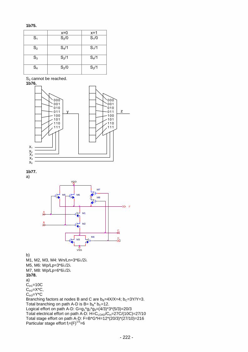
- 222 -
1b75.
S3 cannot be reached. 1b76.
1b77. a)
b)
M1, M2, M3, M4: Wn/Ln=3*6/2
M5, M6: Wp/Lp=3*6/2
M7, M8: Wp/Lp=6*6/2 1b78. a) Cin1=10C Cin2=X*C, Cin3=Y*C Branching factors at nodes B and C are bB=4X/X=4; bC=3Y/Y=3. Total branching on path A-D is B= bB* bC=12. Logical effort on path A-D: G=g1*g2*g3=(4/3)*3*(5/3)=20/3 Total electrical effort on path A-D: H=CLOAD/Cin=27C/(10C)=27/10 Total stage effort on path A-D: F=B*G*H=12*(20/3)*(27/10)=216 Particular stage effort fi=(F)
1/3=6
M6
F
VDD
C
VSS
A
M2B
D
M1
M5M8
M7
M4M3
x=0 x=1
S1 S2/0
S1/0
S2 S4/1
S1/1
S3 S2/1
S4/1
S4 S2/0
S2/1
000 001 010 011 100 101 110 111
z
000 001 010 011 100 101 110 111
y
X1
X2 X3 X4
X5
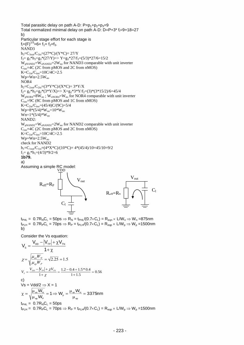
- 223 -
Total parasitic delay on path A-D: P=p1+p2+p3=9 Total normalized minimal delay on path A-D: D=P+3* fi=9+18=27 b) Particular stage effort for each stage is fi=(F)
1/3=6= f1= f2=f3.
NAND3
h3=C3out/C3in=(27*C)/(Y*C)= 27/Y
f3= g3*h3=g3*(27/Y)=> Y=g3*27/f3=(5/3)*27/6=15/2
WpNAND2=WnNAND2=2Wno for NAND3 comparable with unit inverter
Cino=4C (2C from pMOS and 2C from nMOS)
K=C1in/Cino=10C/4C=2.5
Wp=Wn=2.5Wno
NOR4
h2=C2out/C2in=(3*Y*C)/(X*C)= 3*Y/X
f2= g2*h2=g2*(3*Y/X)=> X=g2*3*Y/f2=(3)*(3*15/2)/6=45/4
WpNOR4=8Wno ; WnNOR4=Wno for NOR4 comparable with unit inverter
Cino=9C (8C from pMOS and 1C from nMOS)
K=C2in/Cino=(45/4)C/(9C)=5/4
Wp=8*(5/4)*Wno=10*Wno
Wn=1*(5/4)*Wno
NAND2:
WpNAND2=WnNAND2=2Wno for NAND2 comparable with unit inverter
Cino=4C (2C from pMOS and 2C from nMOS)
K=C1in/Cino=10C/4C=2.5
Wp=Wn=2.5Wno
check for NAND2
h1=C1out/C1in=(4*X*C)/(10*C)= 4*(45/4)/10=45/10=9/2
f1= g1*h1=(4/3)*9/2=6
1b79. a) Assuming a simple RC model:
tPHL = 0.7RNCL = 50ps RN = tPHL/(0.7CL) = Reqn L/Wn Wn =875nm
tPLH = 0.7RPCL = 70ps RP = tPLH/(0.7CL) = Reqp L/Wp Wp =1500nm b)
Consider the Vs equation:
1
VVVV
TNTPDD
S
560511
40514021
1.
.
.*...VVVV
TNTPDD
S
c)
Vs = Vdd/2 X = 1
nm3375W
W1W
W
ep
Nen
p
Pep
Nen
tPHL = 0.7RNCL = 50ps
tPLH = 0.7RPCL = 70ps RP = tPLH/(0.7CL) = Reqp L/Wp Wp =1500nm
enWN
epWP
2.25 1.5
Reff=RP
VDD
Cl
Vout
Reff=Rn Cl
Vout
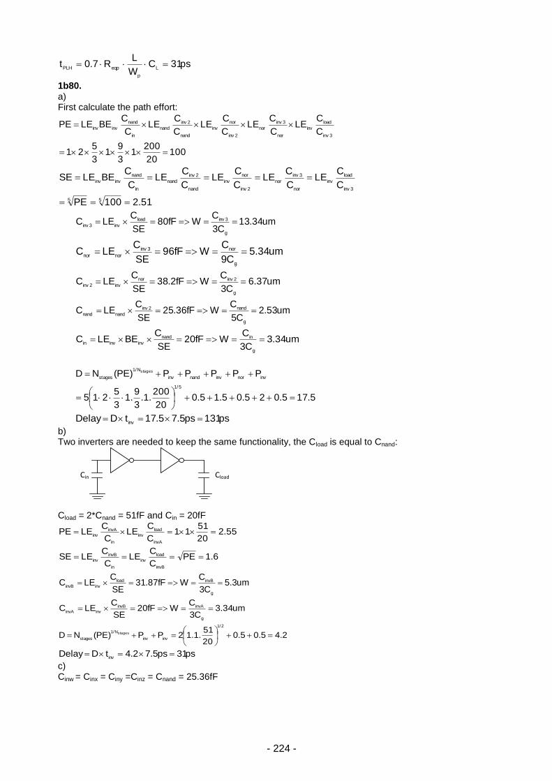
- 224 -
ps31CW
LR7.0t
L
p
eqpPLH
1b80. a) First calculate the path effort:
10020
2001
3
91
3
521
C
CLE
C
CLE
C
CLE
C
CLE
C
CBELEPE
3inv
load
inv
nor
3inv
nor
2inv
nor
inv
nand
2inv
nand
in
nand
invinv
51.2100PE
C
CLE
C
CLE
C
CLE
C
CLE
C
CBELESE
55
3inv
load
inv
nor
3inv
nor
2inv
nor
inv
nand
2inv
nand
in
nand
invinv
um34.13C3
CWfF80
SE
CLEC
g
3invload
inv3inv
um34.5C9
CWfF96
SE
CLEC
g
nor3inv
nornor
um37.6C3
CWfF2.38
SE
CLEC
g
2invnor
inv2inv
um53.2C5
CWfF36.25
SE
CLEC
g
nand2inv
nandnand
um34.3C3
CWfF20
SE
CBELEC
g
innand
invinvin
5.175.025.05.15.020
200.1.
3
9.1
3
5215
PPPPP)PE(ND
5/1
invnorinvnandinv
N/1
stages
stages
ps131ps5.75.17tDDelayinv
b) Two inverters are needed to keep the same functionality, the Cload is equal to Cnand:
Cload = 2*Cnand = 51fF and Cin = 20fF
55.220
5111
C
CLE
C
CLEPE
invA
load
inv
in
invA
inv
6.1PEC
CLE
C
CLESE
invB
load
inv
in
invB
inv
um3.5C3
CWfF87.31
SE
CLEC
g
invBload
invinvB
um34.3C3
CWfF20
SE
CLEC
g
invAinvB
invinvA
2.45.05.020
51.1.12PP)PE(ND
2/1
invinv
N/1
stages
stages
ps31ps5.72.4tDDelayinv
c) Cinw = Cinx = Ciny =Cinz = Cnand = 25.36fF
Cin Cload
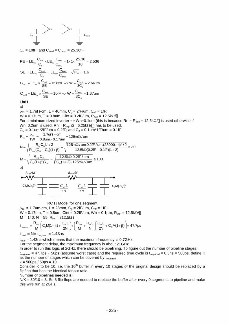
- 225 -
Cin = 10fF; and Cload = Cnand = 25.36fF
536.210
36.2511
C
CLE
C
CLEPE
invA
load
inv
in
invA
inv
6.1PEC
CLE
C
CLESE
invB
load
inv
in
invB
inv
um64.2C3
CWfF85.15
SE
CLEC
g
2invIload
inv2invI
um67.1C3
CWfF10
SE
CLEC
g
invAinvB
inv1invI
1b81. a)
Cu = 1.7u-cm, L = 40mm, Cg = 2fF/um, Ceff = 1fF;
W = 0.17um, T = 0.8um, Cint = 0.2fF/um, Reqn = 12.5k/[]
For a minimum sized inverter => Wn=0.1um (this is because Rn = Reqn = 12.5k/[] is used otherwise if
Wn=0.2um is used, Rn = Reqn /2= 6.25k/[]) has to be used. CG = 0.1um*2fF/um = 0.2fF; and CJ = 0.1um*1fF/um = 0.1fF
um/m125um17.0um8.0
cmu7.1
TWR Cu
int
30)21)(fF1.0fF2.0(k5.12
2/)um28000.(um/fF2.0.um/m125
)1)(CC(R
2/LCRN
2
JGeqn
2
intint
183um/m125)21(C
um/fF2.0.k5.12
R)1(C
CRM
GintG
inteqn
b)
RC Model for one segment
Cu = 1.7um-cm, L = 28mm, Cg = 2fF/um, Ceff = 1fF;
W = 0.17um, T = 0.8um, Cint = 0.2fF/um, Wn = 0.1m, Reqn = 12.5k/[]
M = 140; N = 55; Rint = 212.5k
ps7.47)1(MCN2
LC
N
LR
M
R
N2
LC)1(MC
M
Rt
G
intinteqnint
J
eqn
segment
ns43.1tNtsegmenttotal
ttotal = 1.43ns which means that the maximum frequency is 0.7GHz. For the segment delay, the maximum frequency is about 21GHz. In order to run this logic at 2GHz, there should be pipelining. To figure out the number of pipeline stages:
tsegment = 47.7ps 50ps (assume worst case) and the required time cycle is trequired = 0.5ns = 500ps, define K as the number of stages which can be covered by trequired k = 500ps / 50ps = 10. Consider K to be 10, i.e. the 10
th buffer in every 10 stages of the original design should be replaced by a
flipflop that has the identical fanout ratio. Number of pipelines needed is: N/K = 30/10 = 3. So 3 flip-flops are needed to replace the buffer after every 9 segments to pipeline and make this wire run at 2GHz.
Cin Cload
Reqn/M RintL/N
CJM(1+) CGM(1+)
N
LC
2
int N
LC
2
int
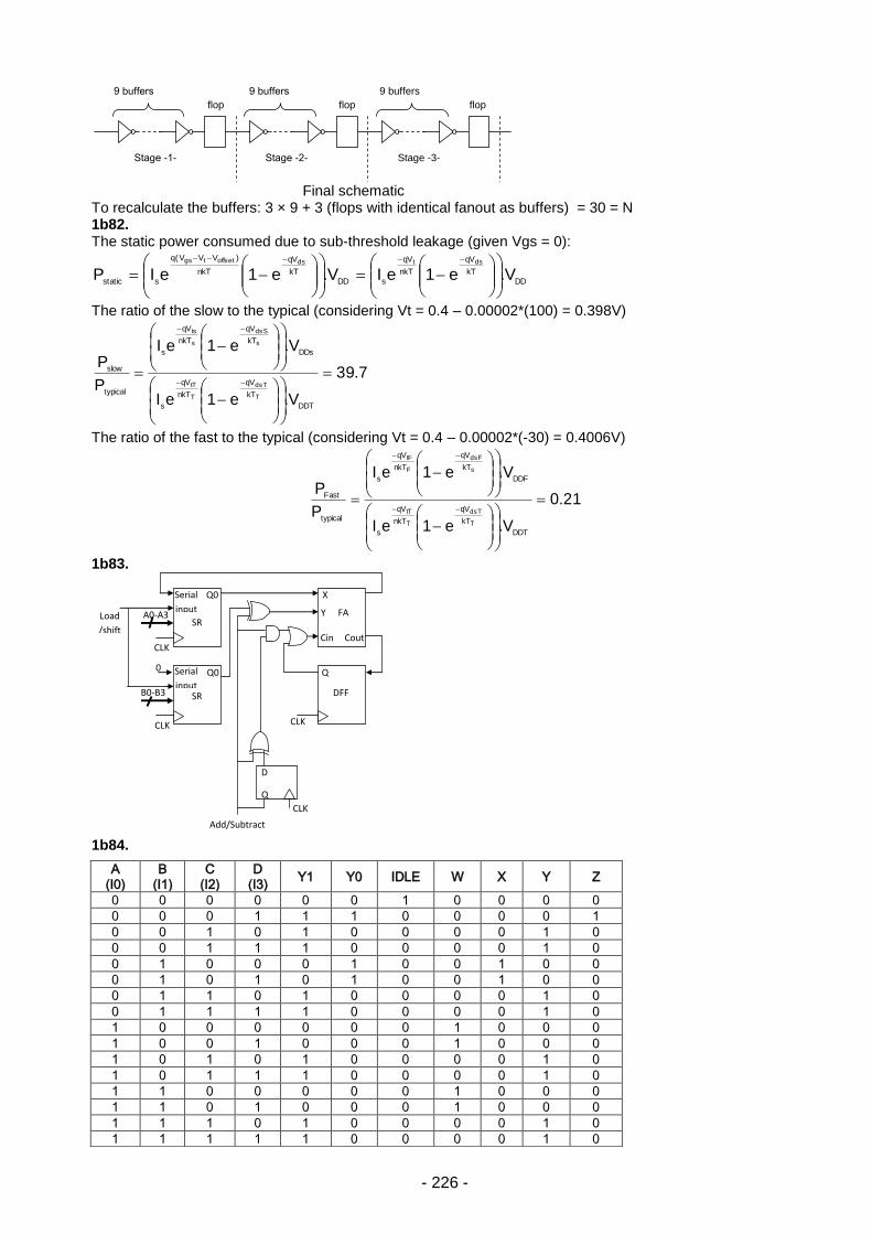
- 226 -
Final schematic
To recalculate the buffers: 3 × 9 + 3 (flops with identical fanout as buffers) = 30 = N 1b82. The static power consumed due to sub-threshold leakage (given Vgs = 0):
DD
kT
qV
nkT
qV
sDD
kT
qV
nkT
)VVV(q
sstaticV.e1eIV.e1eIP
dstdsoffsettgs
The ratio of the slow to the typical (considering Vt = 0.4 – 0.00002*(100) = 0.398V)
7.39
V.e1eI
V.e1eI
P
P
DDT
kT
qV
nkT
qV
s
DDs
kT
qV
nkT
qV
s
typical
slow
T
dsT
T
tT
s
dsS
s
ts
The ratio of the fast to the typical (considering Vt = 0.4 – 0.00002*(-30) = 0.4006V)
21.0
V.e1eI
V.e1eI
P
P
DDT
kT
qV
nkT
qV
s
DDF
kT
qV
nkT
qV
s
typical
Fast
T
dsT
T
tT
s
dsF
F
tF
1b83.
1b84.
9 buffers 9 buffers 9 buffers
flop flop flop
Stage -1- Stage -2- Stage -3-
Add/Subtract
CLK
Serial
input
DFF
Q0
SR
Q0
FA
Serial
input
X
Y
Cin Cout
Q
CLK
CLK
CLK
Load
/shift
D
B0-B3
A0-A3
0
Q
SR
A (I0)
B (I1)
C (I2)
D (I3)
Y1 Y0 IDLE W X Y Z
0 0 0 0 0 0 1 0 0 0 0
0 0 0 1 1 1 0 0 0 0 1
0 0 1 0 1 0 0 0 0 1 0
0 0 1 1 1 0 0 0 0 1 0
0 1 0 0 0 1 0 0 1 0 0
0 1 0 1 0 1 0 0 1 0 0
0 1 1 0 1 0 0 0 0 1 0
0 1 1 1 1 0 0 0 0 1 0
1 0 0 0 0 0 0 1 0 0 0
1 0 0 1 0 0 0 1 0 0 0
1 0 1 0 1 0 0 0 0 1 0
1 0 1 1 1 0 0 0 0 1 0
1 1 0 0 0 0 0 1 0 0 0
1 1 0 1 0 0 0 1 0 0 0
1 1 1 0 1 0 0 0 0 1 0
1 1 1 1 1 0 0 0 0 1 0
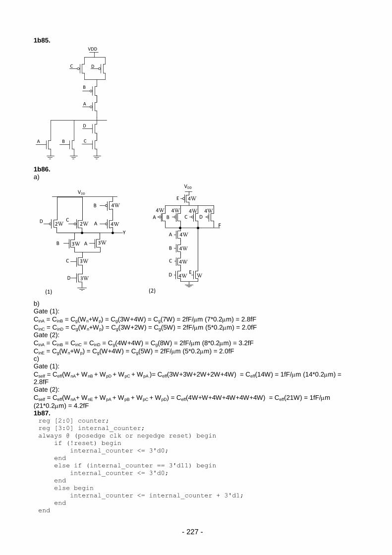
- 227 -
1b85.
1b86. a)
b) Gate (1):
CinA = CinB = Cg(Wn+Wp) = Cg(3W+4W) = Cg(7W) = 2fF/m (7*0.2m) = 2.8fF
CinC = CinD = Cg(Wn+Wp) = Cg(3W+2W) = Cg(5W) = 2fF/m (5*0.2m) = 2.0fF Gate (2):
CinA = CinB = CinC = CinD = Cg(4W+4W) = Cg(8W) = 2fF/m (8*0.2m) = 3.2fF
CinE = Cg(Wn+Wp) = Cg(W+4W) = Cg(5W) = 2fF/m (5*0.2m) = 2.0fF c) Gate (1):
Cself = Ceff(WnA+ WnB + WpD + WpC + WpA )= Ceff(3W+3W+2W+2W+4W) = Ceff(14W) = 1fF/m (14*0.2m) = 2.8fF Gate (2):
Cself = Ceff(WnA+ WnE + WpA + WpB + WpC + WpD) = Ceff(4W+W+4W+4W+4W+4W) = Ceff(21W) = 1fF/m
(21*0.2m) = 4.2fF 1b87. reg [2:0] counter;
reg [3:0] internal_counter;
always @ (posedge clk or negedge reset) begin
if (!reset) begin
internal_counter <= 3'd0;
end
else if (internal_counter == 3'd11) begin
internal_counter <= 3'd0;
end
else begin
internal_counter <= internal_counter + 3'd1;
end
end
A B C
D
A
B
C D
VDD
(1) (2)
D
E
D
E D
C
VDD
F
A
A
B
B
C
VDD
Y
B
A
A
C
C
D
B
2W 2W
4W
4W
3W 3W
3W
3W
4W
4W 4W 4W 4W
4W
4W
4W
4W W
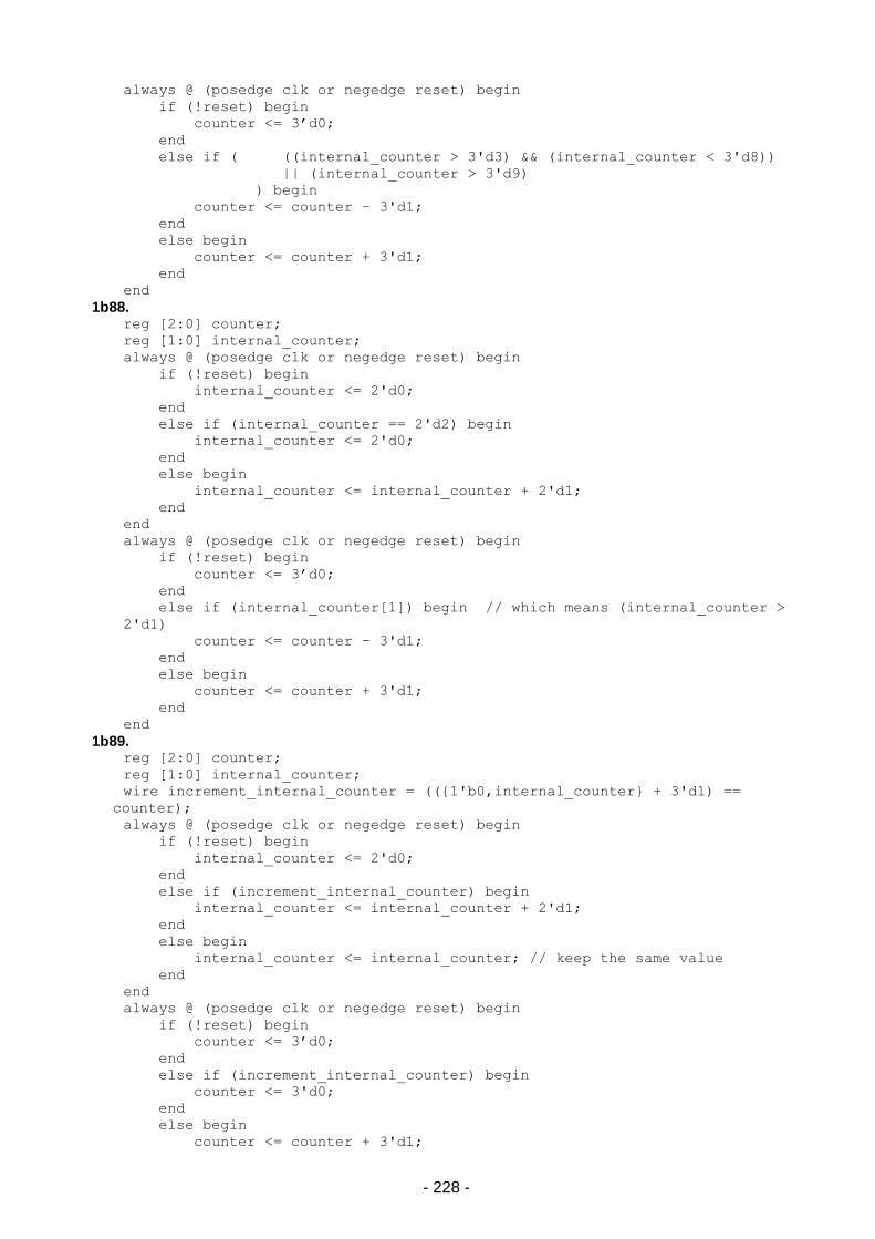
- 228 -
always @ (posedge clk or negedge reset) begin
if (!reset) begin
counter <= 3’d0;
end
else if ( ((internal_counter > 3'd3) && (internal_counter < 3'd8))
|| (internal_counter > 3'd9)
) begin
counter <= counter – 3'd1;
end
else begin
counter <= counter + 3'd1;
end
end
1b88. reg [2:0] counter;
reg [1:0] internal_counter;
always @ (posedge clk or negedge reset) begin
if (!reset) begin
internal_counter <= 2'd0;
end
else if (internal_counter == 2'd2) begin
internal_counter <= 2'd0;
end
else begin
internal_counter <= internal_counter + 2'd1;
end
end
always @ (posedge clk or negedge reset) begin
if (!reset) begin
counter <= 3’d0;
end
else if (internal_counter[1]) begin // which means (internal_counter >
2'd1)
counter <= counter – 3'd1;
end
else begin
counter <= counter + 3'd1;
end
end
1b89. reg [2:0] counter;
reg [1:0] internal_counter;
wire increment_internal_counter = (({1'b0,internal_counter} + 3'd1) ==
counter);
always @ (posedge clk or negedge reset) begin
if (!reset) begin
internal_counter <= 2'd0;
end
else if (increment_internal_counter) begin
internal_counter <= internal_counter + 2'd1;
end
else begin
internal_counter <= internal_counter; // keep the same value
end
end
always @ (posedge clk or negedge reset) begin
if (!reset) begin
counter <= 3’d0;
end
else if (increment_internal_counter) begin
counter <= 3'd0;
end
else begin
counter <= counter + 3'd1;
- 229 -
end
end
1b90. reg [2:0] counter;
reg [2:0] internal_counter;
always @ (posedge clk or negedge reset) begin
if (!reset) begin
internal_counter <= 3'd0;
end
else if (internal_counter == 3'd6) begin
internal_counter <= 3'd0;
end
else begin
internal_counter <= internal_counter + 3'd1;
end
end
always @ (posedge clk or negedge reset) begin
if (!reset) begin
counter <= 3’d0;
end
else if (internal_counter > 3'd4) begin
counter <= counter – 3'd1;
end
else begin
counter <= counter + 3'd1;
end
end
1b91.
Modify the given function into F=AB+AC+ form, implement the function in the structure of dual 4:1 multiplexor, using A and C as selection variables.
1b92.
ABCD Z ABCD Z
0000 0 1000 0
0001 0 1001 0
0010 0 1010 0
0011 1 1011 1
0100 0 1100 1
0101 0 1101 1
0110 0 1110 1
0111 1 1111 1
P1=7/16; P0=9/16 P01 = P0Ē P1=7/16*9/16=63/256=0.246 1b93. For static implementation, energy is consumed in case of 01 transitions of outputs, for dynamic implementation – when the previous state of the output is 0. P=P01VDD
2CĒF
a) P= P01ANDVDD2CĒF+ P01ANDVDD
2CĒF+ P01MUXVDD
2CĒF=(3/16+3/16+1/4)Ē2.5
2 Ē0.3Ē10
12Ē100Ē10
6=
=1.17Ē10-4
W, b) P= P0ANDVDD
2CĒF+ P0ANDVDD
2CĒF+ P0MUXVDD
2CĒF=(3/4+3/4+1/2)Ē2.5
2 Ē0.3Ē10
-12Ē100Ē10
6=
=3.75Ē10-4
W.
A
F
C
A

- 230 -
1b94. The same current flows through both transistors. Vx<4V, the transistor below is not saturated: VDS<VGS-VT, and the transistor above is saturated: VDS=VGS=5-Vx.
22
0
2 ]2
[][2
1DS
DStGStGS V
VVVVV
)2.12.1(39.01|)|2||2(0 xFSBFtt VVVV
x
xxx V
VVV ]
215[))]2.12.1(39.01(5[
2
1 2
Solving this equation, for example by graphical method, this is obtained: Vx=1.09V. Taking W/L=1,
mkVV
KI xx
PD 12.4548.0)24.04(25]2
15[
1b95. Switching point voltage is computed by the following formula:
p
n
TpDDTn
p
n
SP
1
)VV(V
V
Putting switching point and threshold values, denoting n/p ratio by x
2, this is obtained:
1.2=(0.5x+(3.0-0.7))/(1+x), x=1.57, n/p=x2=2.47,
n/p =(Wnkpn/Ln)/(Wpkpp/Lp)= (Wnkpn)/(Wpkpp)= (Wnn)/(Wpp)= 3Wn/Wp=2.47 Wp=3Wn/ 2.47=3Ē 0.5/2.47=0.61 mkm 1b96. Represent the function in the following form:
f(а, b,c) =~a~b + ac + bc = a~b + (a+b)c: On the basis of this expression, the block can be programmed as follows:
f(a,b,c) = (a+b)Mux1 + (a+b)Mux2 = (a+b)c +~a~b. 1b97.
Implement a function of three variables f(a,b,c) = ac + ~a~b. The scheme on the 2:1 multiplexer corresponds to BDD function. To solve the problem, set up a table of the given function. Then, transfer the values of the given function to the scheme on multiplexers.
a b c f
0 0 0 1
0 0 1 1
0 1 0 0
0 1 1 0
1 0 0 0
1 0 1 1
1 1 0 0
1 1 1 1
f
“1”
“0”
“1”
a
b
0
1
0
1 0
1
“0”
“1”
c
Mux 1
Mux 2
- 231 -
1b98. Analyze the given scheme. d1 = ~q1; d2 = q1; t3= q2; Define the characteristic equation of flip-flops: q1*, q2*, q3*.
q1* = d1 =~q1; q2* = d2 = q1; q3* = t3q3= q2q3; On the basis of the characteristic equations, the sequence of states of the scheme is defined. Table of states of the scheme will have the following form:
q1 q2 q3
0 0 0
0 1 0
1 0 1
0 1 1
1 0 0
0 1 0
After the state 010, the sequence of states is repeated. 1b99. Code of one of the numbers, for example A, is given to the input of the decoder, implementing all the minterms of the function of four variables. To construct a scheme, outputs Yi should be connected to the inputs of Di multiplexer which have the same name. The code of the second number is given to address inputs of the multiplexer (in this case B). At coincidence of the codes of numbers A and B, the output of the multiplexer will have "1."
1b100. First transistor groups that connect load transistor with grounding are defined (1 and 3 groups in Figure a). Afterwards taking the sequential or parallel connections of transistors into account, the graph model of logic connections of the circuit is built (Figure b). The logic circuit, corresponding to the obtained graph model is shown in Figure c.
MUX
b2
b1
b0
DC
A0
A1
A2
А3 а1
а2
а3
а0
0
1
2
3
15
0
1
2
3
A0
A1
A2
А3 b3
A= =B
A!=B 15
1
1
0
0
0
c
b
a
y
0
1
0
1
1
0
0
1
0
1
0
1
1
0
1
1B
0‘1’
- 232 -
1b101. Logic 1 is given to C input of D FF. Therefore it operates as signal level repeater, given to D input. In this case there is 0 in its direct output, and 1 in its inverse output. Logic 0 will be formed in the output of “XOR” cell, as the input levels are the same. As there are logic 0s in all address inputs of the decoder, A input signal will be repeated in its 0 output. There will be logic level 1 in all the remaining outputs. 1b102. Logic 1 is always given to the input of an adder with 1 weight. For the LED to light it is necessary to have
logic 0 in the output of the adder with 16 weight, i.e. A+ B ՛ +1<16 inequality occurs. As B՛=15−В, putting it in
the previous inequality, it will turn out that the LED is lit in case of А < В condition. 1b103. 4-bit binary up counter with 16 coefficient is presented. It can change its states from 0 to 15. After getting 16 impulses to the input of a counter, it will again appear in 7 states. In the same state it will appear after 112 impulses the latter being divisible by 16 and the closest to 125. After 13 more impulses it will be in 4 state which will be s hown by the numerical indicator. 1b104. The critical path of a combinatorial circuit is the path with maximum delay. The mobility of an operation is the difference of its as-soon-as-possible (ASAP) start time and as-late-as-possible (ALAP) start time. The critical path in high level synthesis is a path for which all operations on the path have mobility equals zero. 1b105. 1) If there is no data dependency and two functional units that can execute the operations in parallel. 2) If the operations are on alternative branches in the control flow. 1b106. Node index ASAP ALAP Mobility 0 1 3 2 1 1 5 4 2 1 3 2
F
A
NOR
B
E
C
D
AND
AND OR
D
3
4M2
2
1
E
C
B
A
Load transistor
VDD
D
C B A
VSS
E
F
3 2
1
4
Figure a
Figure c Figure b

- 233 -
3 1 4 3 4 1 4 3 5 2 6 4 6 3 5 2 7 3 6 3 8 5 7 2 1b107. 1) TLM communication by function calls, RTL communication by signal protocols 2) TLM offers many timing modeling styles (PV; PVT,…), RTL is always clock driven (cycle-accurate). 1b108.
L1: cyc_wait,L1 = roundup[(4ns-10ns)/10ns] = 0 L2: cyc_wait,L2=roundup[(45ns+4ns-10ns)/10ns]=4 Mem: cyc_wait,mem=roundup[(483ns+45ns+4ns-10ns)/10ns]=53
1b109. cyc_wait,avg= α *0+(1- α)[ β*4+(1- β)*53] For α =β=50%: cyc_wait_avg=14.25
1b110. t_exe =(500 000*CPI + 500 000 * 0.4 * cyc_wait,avg) * t_clock
= (500 000 * 1.6 + 500 000 0.4. * 14.25) * 10ns = 36.5 ms 1b111.
To make the LUT operate in its dual 5-input mode, A6 must be configured to ‘0’ so O6 always takes the output of the upper LUT5. 1b112.
a) f = 1/T = 1/ (4*4ns) = 62.5 MHz b) f = 1/T = 1/ (3*4ns) = 83.3 MHz c) f = 1/T = 1/ (2*4ns) = 125 MHz
1b113. Define: Pi = Ai ⊕ Bi Carry propagate signal Gi = AiBi Carry generate signal Then
Si = Pi ⊕ Ci-1 Ci+1= Gi + PiCi For a 4-bit adder: C1 = G0 + P0C0 C2 = G1 + P1C1 = G1 + P1G0 + P1P0C0 C3 = G2 + P2C2 = G2 + P2G1 + P2P1G0 + P2P1P0C0 C4 = G3 + P3C3 = G3 + P3G2 + P3P2G1 + P3P2P1G0 + P3P2P1P0C0 1b114.
Xi+1 Xi C S2 S1 FFIN
0 0 0 0 0 0
0 0 1 0 1 0
0 1 0 0 1 0
0 1 1 1 0 0
1 0 0 1 0 0
1 0 1 1 1 1
1 1 0 1 1 1
1 1 1 0 0 1
LUT5
LUT5
LUT6
O6
O5
A6
A[5:1] 1 0
- 234 -
1b115.
sv
LTEh
tdt
td
dt
tdv
vv
LTEhvhLTE
t
5
6
4
max
61)310sin(
363
3
2
32
max
max
4
maxmax
2
10102
1022
102)10sin(102))10(cos(
102))10sin(2(
1022
2
1
1b116.
1b117. In order to obtain the same delay of the rising and falling edge of an inverter it is necessary to provide the
same resistivity for nMOS and pMOS transistor. That will happen if Wp/Lp=(n/p)(Wn/Ln)= 2(Wn/Ln). The
smallest inverter with equal delays at rising and falling edge (the unit inverter) will have Wn/Ln =3/2 and
Wp/Lp =6/2. In order to obtain the same falling edge delay for circuit in figure as for the unit inverter, one should
provide that nMOS subcircuit has, in the worst case, the same resistivity as the nMOS transistor in the inverter. In the worst case the slowest falling edge will occur when M4 and at least one of M1, M2, and M3 conducts. Therefore the resistivity of series connection of M4 and (M1 or M2 or M3) should be the same as
the resistivity of the unit nMOS. Therefore W1/L1 = W2/L2 = W3/L3 = W4/L4 = 2(Wn/Ln) = 6/2.
Similarly, to get the same rising edge delay pMOS subcircuit should have the same resistivity as the pMOS transistor of unit inverter. In the worst case the slowest rising edge will occur when M5, M6, and M7 conduct. Therefore the resistivity of series connection of M5, M6 and M7 should be the same as the
resistivity of the unit pMOS. Therefore W5/L5 = W6/L6 = W7/L7 = 3(Wp/Lp) = 18/2. Simultaneously, when
only M8 conducts, the same rising edge will provide W8/L8 = Wp/Lp = 6/2.
1b118. For pMOS subcircuit:
dcbadcbadcbaF OR ) AND AND ( OR ) OR OR ( AND ) OR OR (
For nMOS subcircuit
dcbadcbacbadcbaF AND ) OR OR ( AND ) OR OR (d OR ) OR OR ( AND ) OR OR (
a
b
c
d
VDD
M1 M2 M3
NMOS NMOS NMOS
M5
M6
M7
M8 PMOS
PMOS
PMOS
PMOS
M4
NMOS
- 235 -
2. ANALOG INTEGRATED CIRCUITS a) Test questions 2a1. D 2a2. D 2a3. E 2a4. E 2a5. B 2a6. E 2a7. B 2a8. E 2a9. B 2a10. E 2a11. E 2a12. D 2a13. C 2a14. C 2a15. C 2a16. A 2a17. C 2a18. C 2a19. E 2a20. A 2a21. C 2a22. D 2a23. D 2a24. D 2a25. E 2a26. D 2a27. E 2a28. E 2a29. D 2a30. B 2a31. A 2a32. B 2a33. E 2a34. C 2a35. B 2a36. C 2a37. C 2a38. E 2a39. B 2a40. C 2a41. B
2a42. E 2a43. B 2a44. D 2a45. C 2a46. D 2a47. E 2a48. A 2a49. E 2a50. E 2a51. D 2a52. E 2a53. C 2a54. A 2a55. D 2a56. A 2a57. D 2a58. C 2a59. B 2a60. B 2a61. A 2a62. D 2a63. A 2a64. D 2a65. A 2a66. D 2a67. C 2a68. D 2a69. A 2a70. B 2a71. A 2a72. B 2a73. C 2a74. C 2a75. B 2a76. B 2a77. E 2a78. C 2a79. E 2a80. B 2a81. A 2a82. C
2a83. B 2a84. C 2a85. E 2a86. C 2a87. B 2a88. B 2a89. C 2a90. A 2a91. A 2a92. D 2a93. A 2a94. B 2a95. C 2a96. A 2a97. A 2a98. A 2a99. D 2a100. B 2a101. C 2a102. C 2a103. B 2a104. B 2a105. C 2a106. D 2a107. D 2a108. C 2a109. A 2a110. B 2a111. C 2a112. C 2a113. A 2a114. B 2a115. A 2a116. D 2a117. B 2a118. E 2a119. D 2a120. B 2a121. C 2a122. B 2a123. C
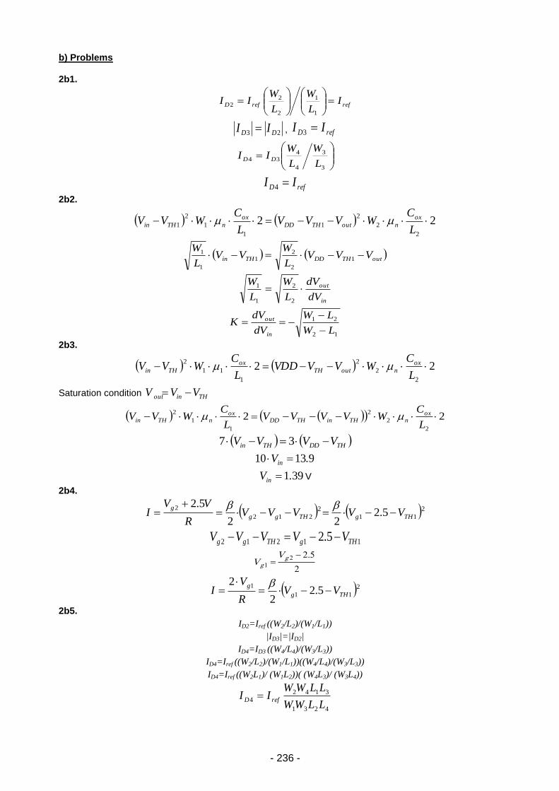
- 236 -
b) Problems 2b1.
refrefD IL
W
L
WII
1
1
2
22
23 DD II , refD II 3
3
3
4
434
L
W
L
WII DD
refD II 4
2b2.
222
2
2
1
1
1
2
1 L
CWVVV
L
CWVV ox
noutTHDDox
nTHin
outTHDDTHin VVVL
WVV
L
W 1
2
21
1
1
in
out
dV
dV
L
W
L
W
2
2
1
1
12
21
LW
LW
dV
dVK
in
out
2b3.
222
2
2
1
11
2
L
CWVVVDD
L
CWVV ox
noutTHox
THin
Saturation condition THinout VVV
222
2
2
1
1
2
L
CWVVVV
L
CWVV ox
nTHinTHDDox
nTHin
THDDTHin VVVV 37
91310 .Vin
391.Vin V
2b4.
211
2
212
25.2
22
5.2THgTHgg
gVVVVV
R
VVI
11212 5.2 THgTHgg VVVVV
2
5221
.VV
gg
211
15.2
2
2THg
gVV
R
VI
2b5.
ID2=Iref ((W2/L2)/(W1/L1))
|ID3|=|ID2|
ID4=ID3 ((W4/L4)/(W3/L3))
ID4=Iref ((W2/L2)/(W1/L1))((W4/L4)/(W3/L3))
ID4=Iref ((W2L1)/ (W1L2))( (W4L3)/ (W3L4))
4231
3142
4LLWW
LLWWII refD
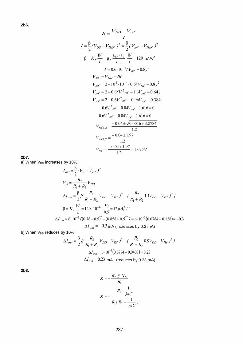
- 237 -
2b6.
I
VVR refDD
22
22)VV()VV(I THNrefTHNGS
ββ
1200
L
W
tL
WK
ox
Sinn
εεμβ uA/V
2
24 801060 ).V(.I ref
3840960602
64061602
806010102
2
2
244
.V.V.V
).V.V(.V
).V(.V
IRVV
refrefref
refrefref
refref
DDref
0616104060
0616104060
2
2
.V.V.
.V.V.
refref
refref
V 675121
971040
21
971040
21
8784300160040
21
21
..
..V
.
..V
.
...V
ref
,ref
,ref
2b7. a) When VDD increases by 10%.
26
2
21
22
21
2
21
2
2
1250
5010120
112
2
VA.L
WK
])VV.RR
R()VV
RR
R[(I
VRR
RV
)VV(I
n
THDDTHDDout
DDA
THAout
μβ
β
β
3012800784010650858050780106 3223 ...]....[I out
30.I out mA (increases by 0.3 mA)
b) When VDD reduces by 10%.
])VV.RR
R()VV
RR
R[(I THDDTHDDout
2
21
22
21
2 902
β
2300408007840106 3 ...I out
230.I out mA (reduces by 0.23 mA)
2b8.
)Cj
R(R
CjR
K
R
X||RK C
ω
ω
1
1
21
2
1
2
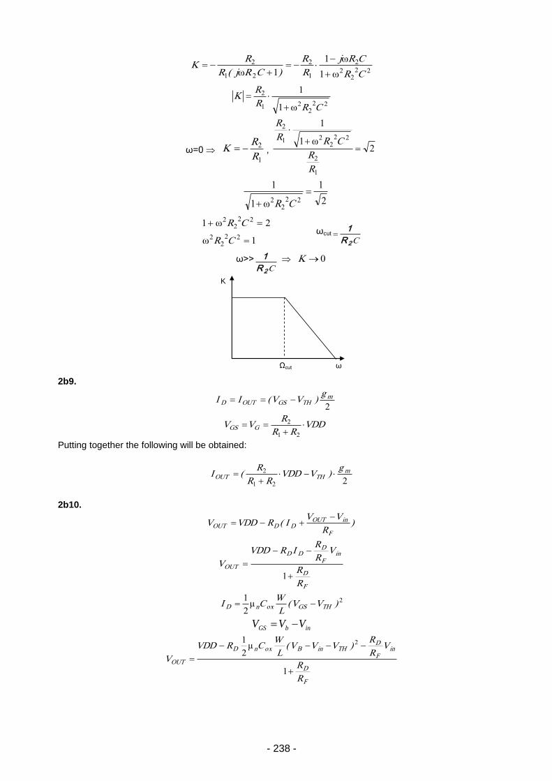
- 238 -
222
2
2
1
2
21
2
1
1
1 CR
CRj
R
R
)CRj(R
RK
ω
ω
ω
222
21
2
1
1
CRR
RK
ω
ω=0 1
2
R
RK , 2
1
1
1
2
222
21
2
R
R
CRR
R
ω
2
1
1
1
222
2
CRω
1
21
222
2
222
2
CR
CR
ω
ω ωcut
C2R
1
ω>>C2R
1 0K
2b9.
2
mTHGSOUTD
g)VV(II
VDDRR
RVV GGS
21
2
Putting together the following will be obtained:
221
2 mTHOUT
g)VVDD
RR
R(I
2b10.
)R
VVI(RVDDV
F
inOUTDDOUT
F
D
inF
DDD
OUT
R
R
VR
RIRVDD
V
1
2
2
1)VV(
L
WCI THGSoxnD μ
inbGS VVV
F
D
inF
DTHinBoxnD
OUT
R
R
VR
R)VVV(
L
WCRVDD
V
1
2
1 2μ
K
ω Ωcut
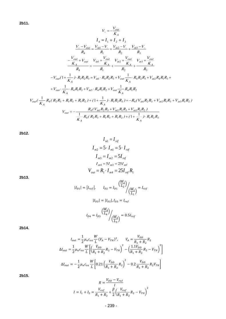
- 239 -
2b11.
A
out
K
VV
3214 IIII
3
3
2
2
1
1
4 R
VV
R
VV
R
VV
R
VV inininout
3
3
2
2
1
1
4 R
K
VV
R
K
VV
R
K
VV
R
VK
V
A
outin
A
outin
A
outinout
A
out
2142143314
31423243241321
11
111
RRRK
VRRRVRRRK
V
RRRVRRRK
VRRRVRRR)K
(V
Aoutin
Aout
inA
outinA
out
)RRVRRVRRV(R)RRR)K
()RRRRRR(RK
(V inininAA
out 21331232143212131324
11
1
3212131324
2133123214
11
1RRR)
K()RRRRRR(R
K
)RRVRRVRRV(RV
AA
inininout
2b12.
refm II 1
refmm III 55 12
refmm III 523
refmm III 255 34
141 25 RIIRV refmout
2b13.
| | ( )
( )
⁄
( )
( )
⁄
2b14.
( )
[(
)
(
)
]
[ (
)
]
2b15.
(
)
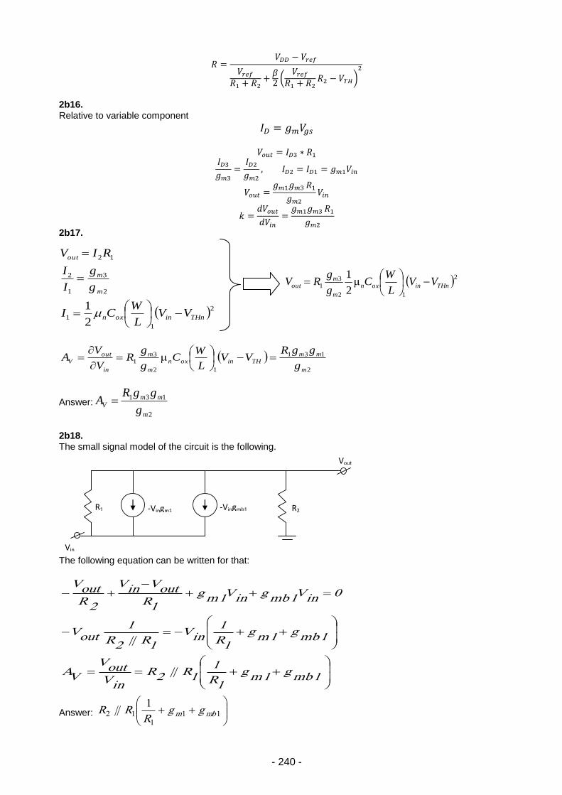
- 240 -
(
)
2b16. Relative to variable component
2b17.
2
131
12
31 μ
m
mmTHinoxn
m
m
in
outV
g
ggRVV
L
WC
g
gR
V
VA
Answer:
2
131
m
mmV
g
ggRA
2b18. The small signal model of the circuit is the following.
The following equation can be written for that:
1mbg1mg
1R
11R||2R
inVoutV
VA
1mbg1mg
1R
1inV
1R||2R
1outV
0inV1mbginV1mg
1RoutVinV
2RoutV
Answer:
11
112
1mbm gg
RR||R
R1 -Vingm1 -Vingmb1 R2
Vin
Vout
2
1
1
2
3
1
2
12
2
1THninoxn
m
m
out
VVL
WCI
g
g
I
I
RIV
2
12
31 μ
2
1THninoxn
m
mout VV
L
WC
g
gRV
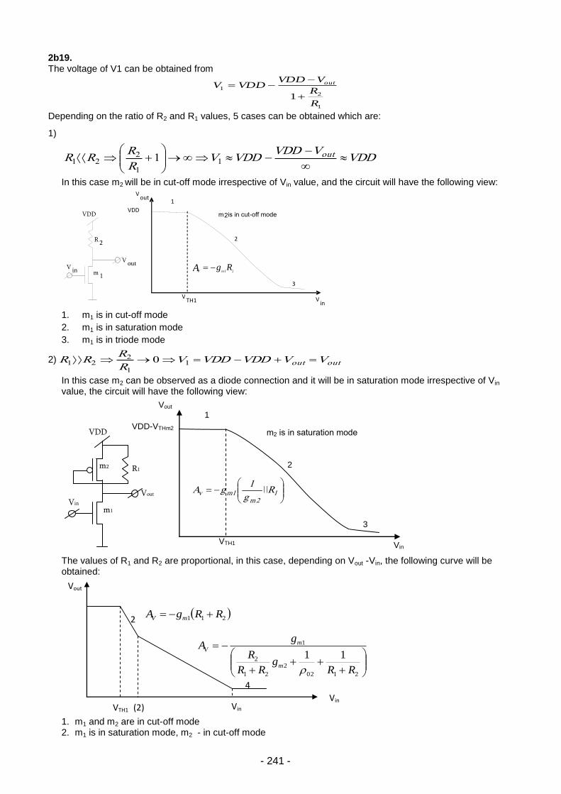
- 241 -
2b19. The voltage of V1 can be obtained from
1
21
1R
R
VVDDVDDV out
Depending on the ratio of R2 and R1 values, 5 cases can be obtained which are:
1)
VDDVVDD
VDDVR
RRR out
1
1
221 1
In this case m2 will be in cut-off mode irrespective of Vin value, and the circuit will have the following view:
1. m1 is in cut-off mode
2. m1 is in saturation mode
3. m1 is in triode mode
2) outout VVVDDVDDVR
RRR 1
1
221 0
In this case m2 can be observed as a diode connection and it will be in saturation mode irrespective of Vin value, the circuit will have the following view:
The values of R1 and R2 are proportional, in this case, depending on Vout -Vin, the following curve will be obtained:
1. m1 and m2 are in cut-off mode 2. m1 is in saturation mode, m2 - in cut-off mode
V out
V in
V TH1
2
3
VDD
1
m 1
R 2
VDD
V out V in
m 2 is in cut - off mode
2 1 R g A m V
2102
2
21
2
1
11
RRg
RR
R
gA
m
mV
Vout
Vin
VTH1 (2) Vin
211 RRgA mV 2
4
Vout
Vin VTH1
2
3
VDD-VTHm2
1
m1
R1
VDD
Vout
Vin
m2
m2 is in saturation mode
1
2m1mv R\\
g
1gA
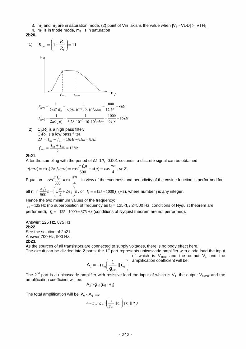
- 242 -
3. m1 and m2 are in saturation mode, (2) point of Vin axis is the value when |V1 - VDD| > |VTH2| 4. m1 is in triode mode, m2 is in saturation
2b20.
1) 1111
3
R
RKcut
Hz.ohm.RC
f
Hz.ohm,RC
f
cut
cut
16862
1000
101010286
1
2
1
85612
1000
10210286
1
2
1
3632
2
3521
1
π
π
2) C1,R2 is a high pass filter. C2R3 is a low pass filter.
Hzff
f
HzHzHzfff
ktkt
kentr
ktkt
122
8816
21
12
2b21. After the sampling with the period of Δt=1/fs=0.001 seconds, a discrete signal can be obtained
00( ) cos 2 cos
500
f nu n t f n t
= ( ) cos
4
nx n
, nZ.
Equation 0cos500
f n= cos
4
n
in view of the evenness and periodicity of the cosine function is performed for
all n, if 0 2500 4
fn j n
, or 0 125 1000f j (Hz), where number j is any integer.
Hence the two minimum values of the frequency:
0 125f Hz (no superposition of frequency as f0 = 125<fs / 2=500 Hz, conditions of Nyquist theorem are
performed), 0 125 1000 875f Hz (conditions of Nyquist theorem are not performed).
Answer: 125 Hz, 875 Hz. 2b22. See the solution of 2b21. Answer 700 Hz, 900 Hz. 2b23. As the sources of all transistors are connected to supply voltages, there is no body effect here. The circuit can be divided into 2 parts: the 1
st part represents unicascade amplifier with diode load the input
of which is Vinput and the output V1 and the amplification coefficient will be:
The 2nd
part is a unicascade amplifier with resistive load the input of which is V1, the output Voutput and the amplification coefficient will be:
A2=-gm3(r03||R1)
The total amplification will be 21
AA
)R||r(r||g
ggAm
mm 10301
2
31
1
f Fcut1 Fcut2
k
01
2m
1m1r||
g
1gA
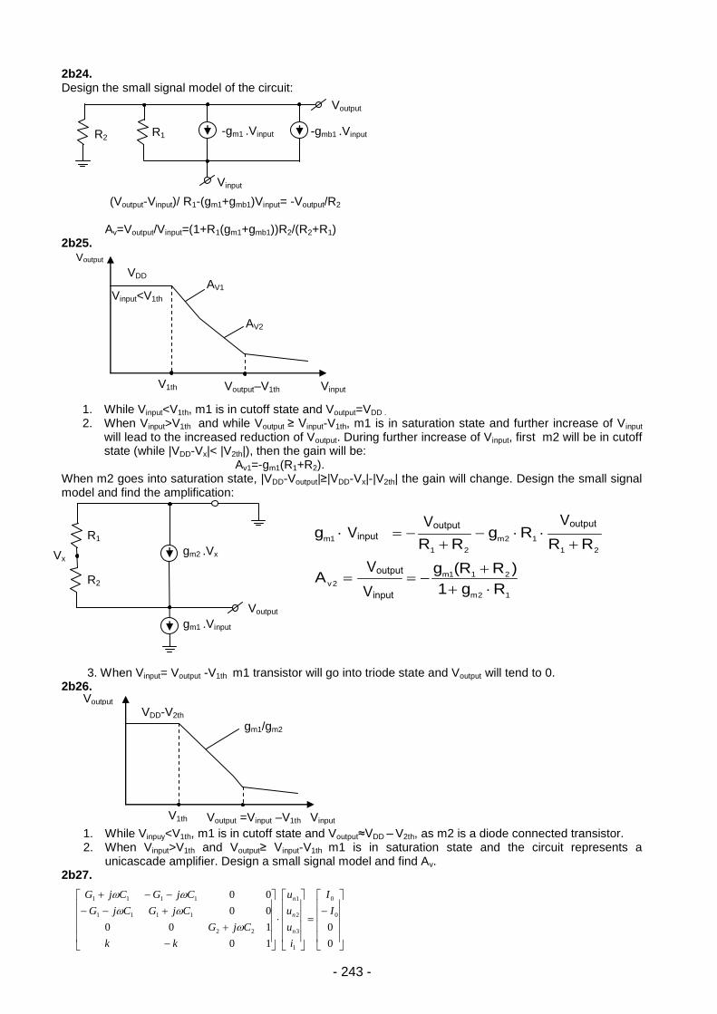
- 243 -
2b24. Design the small signal model of the circuit:
(Voutput-Vinput)/ R1-(gm1+gmb1)Vinput= -Voutput/R2
Av=Voutput/Vinput=(1+R1(gm1+gmb1))R2/(R2+R1) 2b25.
1. While Vinput<V1th, m1 is in cutoff state and Voutput=VDD . 2. When Vinput>V1th and while Voutput ≥ Vinput-V1th, m1 is in saturation state and further increase of Vinput
will lead to the increased reduction of Voutput. During further increase of Vinput, first m2 will be in cutoff state (while |VDD-Vx|< |V2th|), then the gain will be:
Av1=-gm1(R1+R2). When m2 goes into saturation state, |VDD-Voutput|≥|VDD-Vx|-|V2th| the gain will change. Design the small signal model and find the amplification:
3. When Vinput= Voutput -V1th m1 transistor will go into triode state and Voutput will tend to 0. 2b26.
1. While Vinpuy<V1th, m1 is in cutoff state and Voutput≈VDD – V2th, as m2 is a diode connected transistor. 2. When Vinput>V1th and Voutput≥ Vinput-V1th m1 is in saturation state and the circuit represents a
unicascade amplifier. Design a small signal model and find Av. 2b27.
-gmb1 .Vinput R1
Voutput
R2 -gm1 .Vinput
Vinput
R1
Vx
Voutput
gm1 .Vinput
gm2 .Vx
R2 Vinput
Voutput
Voutput Voutput Vinput
12m
211m
2v
21
12m
21
1m
Rg1
)RR(gA
RRRg
RRg
VDD
V1th Voutput–V1th Vinput
AV1
Voutput
Vinput<V1th
AV2
VDD-V2th
V1th Voutput =Vinput –V1th Vinput
gm1/gm2
Voutput
0
0
10
100
00
00
0
0
1
3
2
1
22
1111
1111
I
I
i
u
u
u
kk
CjG
CjGCjG
CjGCjG
n
n
n

- 244 -
2b28. a)
Vtnew = 0.4 – 0.1 = 0.3V
8.0vWCv4.02.1WCIsatoxsatoxds ; and
9.0vWCv3.02.1WCIsatoxsatoxds
the saturation current will increase by x1.125 b)
063.0eee1eIe1eII
I )1.0(nkT
q)VV(
nkT
q
kT
qV
nkT
qV
s
kT
qV
nkT
qV
s
2sub
1sub 1t2tdd2tdd1t
Isub2/Isub1 = 15.8 c)
Changing Vt and T
0089.0e1eIe1eII
I2kT
qV
2nkT
qV
s
1kT
qV
1nkT
qV
s
2sub
1subdd2tdd1t
Isub2/Isub1 = 112.35
Changing T only
0733.0e1eIe1eII
I2kT
qV
2nkT
qV
s
1kT
qV
1nkT
qV
s
2sub
1subdd1tdd1t
Isub2/Isub1 = 13.64
The sub-threshold leakage will increase as the temperature increase,
d) Assume that the threshold voltage has to be reduced by increasing the body voltage (using body effect), what would be the value of Vsb to reach the targeted Vt.
)||2V||2(4.0VFsbFt ; then
)88.0V88.0(2.04.03.0sb => V688.0V
sb
2b29. Approximate Vt0 and tox then:
sat
ctgs
2
tgs
oxds.
LEVV
VVWCI
Assume EcL = 0, then
sattgsoxds
.VVWCI
Substitute for Ids1 = 78.70A and Vgs1 = 1.2 V and Ids2 = 56.21A and Vgs2 = 1.0V then:
4.1V0.1
V2.1
VV
VV
I
I
0t
0t
0t2gs
0t1gs
2ds
1ds
Vt0 = 0.5V
substitute in one of the two equations, then tox = 10 nm. 2b30. W = 900nm; L = 180nm; and xd = 20nm;
2
8
14
ox
ox
oxcm/F87
10*40
10*85.8*97.3
tC
fF141fF10*180*900*87WLC 5
ox
cm/nF566.1cm10*180*cm/F10*87LCC 726
oxg
fF66.15fF10*20*900*87WxCC 5
doxol
2Col+WLCox = 172.32fF
Operation Region
Cgb Cgs Cgd CG
Cutoff WLC
ox
141fF 0 0 olox
C2WLC
172.32fF
Linear 0 2/WLC
ox
70.5fF
2/WLCox 70.5fF
oloxC2WLC
172.32fF
Saturation 0 3/WLC2
ox 94fF
0 oloxC23/WLC2
125.32fF
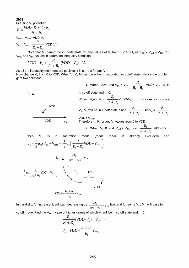
- 245 -
VDD
Vx
Ix=0
Ix
2b31. First find V1 potential:
21
211
RR
RVRVDDV x
VDS1: VDS1=VDD-Vx
Vgs1: Vgs1=
21
1
RR
R
(VDD-Vx)
Note that M1 cannot be in triode state for any values of Vx from 0 to VDD, as VDS1> Vgs1 – VTH: Put VDS1 and Vgs1 values in saturation inequality condition:
1
21
1 )( THxx VVVDDRR
RVVDD
As all the inequality members are positive, it is correct for any Vx. Now change Vx from 0 to VDD. When Vx=0, M1 can be either in saturation or cutoff state. Hence the problem gets two solutions:
1. When Vx=0 and Vgs1< VTH -
21
1
RR
R
VDD< VTH, M1 is
in cutoff state and Ix=0.
When Vx≠0, Vgs1=
21
1
RR
R
(VDD-Vx). In this case for positive
Vx, M1 will be in cutoff state since
21
1
RR
R
(VDD-Vx)<
21
1
RR
R
VDD< VTH1. Therefore Ix=0, for any Vx values from 0 to VDD.
2. When Vx=0 and Vgs1> VTH1, i.e.
21
1
RR
R
VDD>VTH1,
then M1 is in saturation mode (triode mode is already excluded) and
1
21
111
2
1)(
2
1THmTHgsmx VVDD
RR
RgVVgI .
In parallel to Vx increase, Ix will start decreasing by mg
xvv
xI
)1(
law, and for some Vx , M1 will pass to
cutoff mode. Find the Vx, in case of higher values of which M1 will be in cutoff state and Ix=0.
THx VVVDDRR
R)(
21
1
1
1
21THx V
R
RRVDDV
VDD Vx
Ix=0
Ix
mg
xvv
xI
)1(
1
1
21THV
R
RRVDD
1
21
1
2
1THm VVDD
RR
Rg
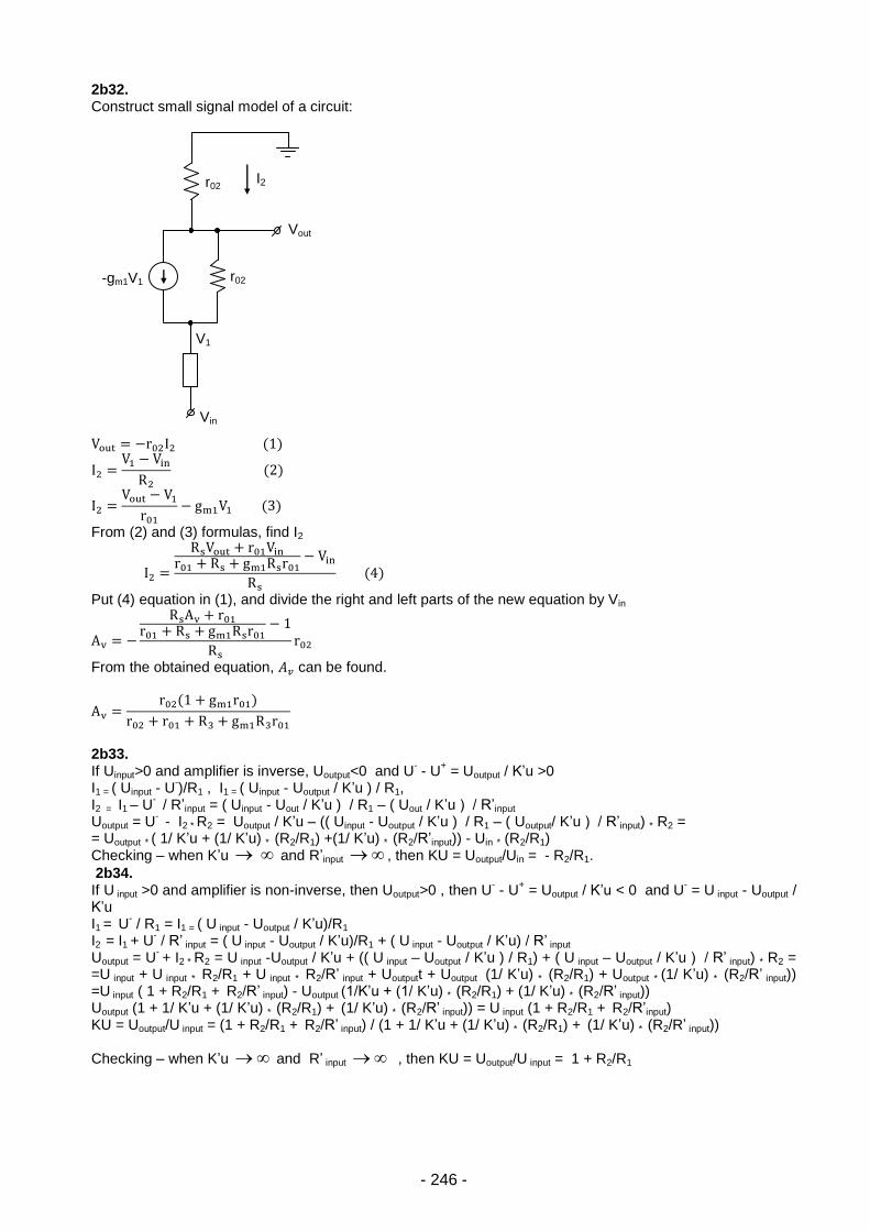
- 246 -
2b32. Construct small signal model of a circuit:
( )
( )
( )
From (2) and (3) formulas, find I2
( )
Put (4) equation in (1), and divide the right and left parts of the new equation by Vin
From the obtained equation, can be found.
( )
2b33. If Uinput>0 and amplifier is inverse, Uoutput<0 and U
- - U
+ = Uoutput / K’u >0
I1 = ( Uinput - U-)/R1 , I1 = ( Uinput - Uoutput / K’u ) / R1,
I2 = I1 – U- / R’input = ( Uinput - Uout / K’u ) / R1 – ( Uout / K’u ) / R’input
Uoutput = U- - I2 * R2 = Uoutput / K’u – (( Uinput - Uoutput / K’u ) / R1 – ( Uoutput/ K’u ) / R’input) * R2 =
= Uoutput * ( 1/ K’u + (1/ K’u) * (R2/R1) +(1/ K’u) * (R2/R’input)) - Uin * (R2/R1) Checking – when K’u and R’input , then KU = Uoutput/Uin = - R2/R1.
2b34. If U input >0 and amplifier is non-inverse, then Uoutput>0 , then U
- - U
+ = Uoutput / K’u < 0 and U
- = U input - Uoutput /
K’u I1 = U
- / R1 = I1 = ( U input - Uoutput / K’u)/R1
I2 = I1 + U- / R’ input = ( U input - Uoutput / K’u)/R1 + ( U input - Uoutput / K’u) / R’ input
Uoutput = U- + I2 * R2 = U input -Uoutput / K’u + (( U input – Uoutput / K’u ) / R1) + ( U input – Uoutput / K’u ) / R’ input) * R2 =
=U input + U input * R2/R1 + U input * R2/R’ input + Uoutputt + Uoutput (1/ K’u) * (R2/R1) + Uoutput * (1/ K’u) * (R2/R’ input)) =U input ( 1 + R2/R1 + R2/R’ input) - Uoutput (1/K’u + (1/ K’u) * (R2/R1) + (1/ K’u) * (R2/R’ input)) Uoutput (1 + 1/ K’u + (1/ K’u) * (R2/R1) + (1/ K’u) * (R2/R’ input)) = U input (1 + R2/R1 + R2/R’input) KU = Uoutput/U input = (1 + R2/R1 + R2/R’ input) / (1 + 1/ K’u + (1/ K’u) * (R2/R1) + (1/ K’u) * (R2/R’ input)) Checking – when K’u and R’ input , then KU = Uoutput/U input = 1 + R2/R1
r02 I2
r02
Vout
-gm1V1
V1
Vin

- 247 -
3. RF CIRCUITS
a) Test questions 3a1. A 3a2. A 3a3. B
- 248 -
4. SEMICONDUCTOR PHYSICS AND ELECTRONIC DEVICES
a) Test questions 4a1. D 4a2. A 4a3. B 4a4. C 4a5. B 4a6. B 4a7. C 4a8. C 4a9. A 4a10. B 4a11. A 4a12. C 4a13. B 4a14. D 4a15. E 4a16. A 4a17. C 4a18. C 4a19. C 4a20. B 4a21. E 4a22. C 4a23. C 4a24. C 4a25. E 4a26. C 4a27. B 4a28. C 4a29. C 4a30. A 4a31. D 4a32. E 4a33. C 4a34. C 4a35. B 4a36. C 4a37. C 4a38. C 4a39. B 4a40. D 4a41. D 4a42. D 4a43. B 4a44. B 4a45. B 4a46. B 4a47. C 4a48. A 4a49. D 4a50. B 4a51. A
4a52. B 4a53. C 4a54. C 4a55. B 4a56. B 4a57. B 4a58. C 4a59. B 4a60. D 4a61. D 4a62. C 4a63. C 4a64. C 4a65. C 4a66. C 4a67. C 4a68. E 4a69. C 4a70. C 4a71. D 4a72. B 4a73. E 4a74. E 4a75. D 4a76. E 4a77. C 4a78. A 4a79. E 4a80. D 4a81. C 4a82. C 4a83. B 4a84. A 4a85. D 4a86. A 4a87. C 4a88. D 4a89. B 4a90. A 4a91. C 4a92. D 4a93. B 4a94. E 4a95. D 4a96. C 4a97. B 4a98. D 4a99. B 4a100. B 4a101. E 4a102. E
4a103. C 4a104. D 4a105. A 4a106. B 4a107. E 4a108. B 4a109. A 4a110. D 4a111. E 4a112. A 4a113. B 4a114. D 4a115. A 4a116. D 4a117. B 4a118. A 4a119. B 4a120. B 4a121. A 4a122. A 4a123. B 4a124. C 4a125. B 4a126. B 4a127. B 4a128. A 4a129. C 4a130. B 4a131. D 4a132. C 4a133. B 4a134. D 4a135. A 4a136. C 4a137. E 4a138. B 4a139. E 4a140. C 4a141. A 4a142. C 4a143. C 4a144. E 4a145. B 4a146. B 4a147. E 4a148. C 4a149. D 4a150. B 4a151. B 4a152. B 4a153. B
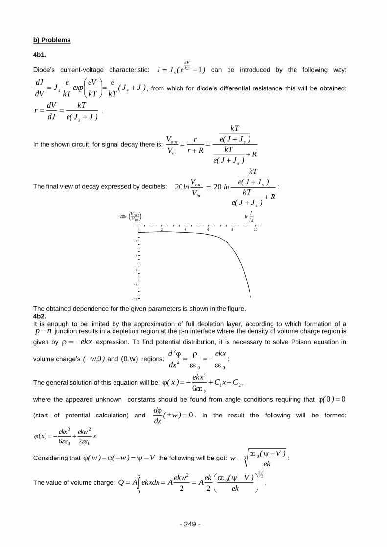
- 249 -
b) Problems 4b1.
Diode’s current-voltage characteristic: )e(JJ kT
eV
s 1
can be introduced by the following way:
)JJ(kT
e
kT
eVexp
kT
eJ
dV
dJss
, from which for diode’s differential resistance this will be obtained:
)JJ(e
kT
dJ
dVr
s .
In the shown circuit, for signal decay there is:
R)JJ(e
kT
)JJ(e
kT
Rr
r
V
V
s
s
in
out
The final view of decay expressed by decibels:
R)JJ(e
kT
)JJ(e
kT
lnV
Vln
s
s
in
out
2020 :
The obtained dependence for the given parameters is shown in the figure. 4b2. It is enough to be limited by the approximation of full depletion layer, according to which formation of a
np junction results in a depletion region at the p-n interface where the density of volume charge region is
given by ekx expression. To find potential distribution, it is necessary to solve Poison equation in
volume charge’s ),w( 0 and )w,(0 regions:
00
2
2
ekx
dx
d:
The general solution of this equation will be: 21
0
3
6CxC
ekx)x(
,
where the appeared unknown constants should be found from angle conditions requiring that 00 )(
(start of potential calculation) and 0
)w(dx
d. In the result the following will be formed:
.26
)(0
2
0
3
xekwekx
x
Considering that V)w()w( the following will be got: 3 0
ek
)V(w
:
The value of volume charge: 3
2
0
2
022
ek
)V(ekA
ekwAekxdxAQ
w
,
- 2
- 4
- 6
- 8
- 10
2 4 6 8 10
ln 𝐽
𝐽𝑆 20ln (
𝑜
)
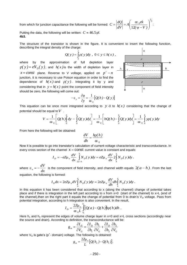
- 250 -
from which for junction capacitance the following will be formed:
31
0
12
)V(
ekA
dV
dQC :
Putting the data, the following will be written: 546.C pf.
4b3. The structure of the transistor is shown in the figure. It is convenient to insert the following function, describing the integral density of the charge:
y
,)x(hy,dy)y()y(Q0
0
where by the approximation of full depletion layer
)y(eN)y( D , and )x(h is the width of depletion layer in
constx plane. Reverse to V voltage, applied on np
junction, it is necessary to use Poison equation in order to find the
dependence of )x(h -and )y( . Integrating it by y and
considering that in )x(hy point the component of field intensity
should be zero, the following will come out:
)y(Q)h(Qy
y
0
1
This equation can be once more integrated according to y -0 to )x(h considering that the change of
potential should be equal toV .
hhh h
dy)y(ydy)y(Q)h(hQdy)y(Qdy)h(QV00000 00
111
From here the following will be obtained:
0
)h(h
dh
dV
Now it is possible to go into transistor’s calculation of current-voltage characteristic and transconductance. In
every cross section of the channel constx current value is constant and equals:
a
h
Dn
h
ha
DnD dy)y(Ndx
dVeZdy)y(N
dx
dVeZI 2
2
,
where dx
dVx is the component of field intensity, and channel width equals )ha( 2 . From the last
equation, the following is formed:
a
h
D
a
h
nDnD dy)y(Ndhdh
dVeZdy)y(NdVeZdxI 22 ,
In this equation it has been considered that according to x (along the channel) change of potential takes place and if there is integration in the left part according to x from x=0 (start of the channel) to x=L (end of the channel),then on the right part it equals the change of potential from 0 to drain’s VD voltage. Pass from potential integration, according to h integration is also convenient. In the result,
dh)h(h)h(Q)a(QL
ZI
h
h
n
D
2
10
2,
Here h1 and h2 represent the edges of volume charge layer in x=0 and x=L cross sections (accordingly near the source and drain). According to definition, the transconductance will be:
G
D
G
D
G
Dm
V
h
h
I
V
h
h
I
V
Ig
2
2
1
1
where VG is gate’s (p+- domain) voltage. The following is obtained:
)h(Q)h(QL
Zg n
m 12
2
.
h1 h2
a
p+
p+
Ф
Ф
А B
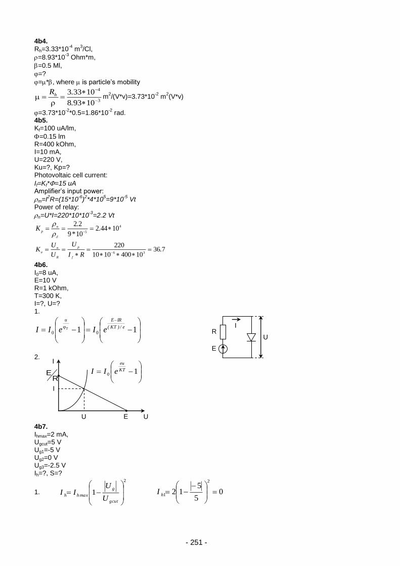
- 251 -
4b4. Rh=3.33*10
-4 m
3/Cl,
=8.93*10-3
Ohm*m,
=0.5 Ml,
=?
=*, where is particle’s mobility
3
4
10938
10333
.
.Rh m2/(V*v)=3.73*10
-2 m
2(V*v)
=3.73*10-2
*0.5=1.86*10-2
rad. 4b5. Kf=100 uA/lm,
=0.15 lm R=400 kOhm, I=10 mA, U=220 V, Ku=?, Kp=? Photovoltaic cell current:
If=Kf*=15 uA Amplifier’s input power:
m=I2R=(15*10
-6)2*4*10
5=9*10
-5 Vt
Power of relay:
n=U*I=220*10*10-3
=2.2 Vt
4
510442
109
22
.
*
.K n
p
736104001010
22036
.RI
U
U
UK
f
p
R
n
u
4b6. I0=8 uA, E=10 V R=1 kOhm, T=300 K, I=?, U=? 1.
11 00
e/)KT(
IREu
eIeII T
2. 4b7. Ihmax=2 mA, Ugcut=5 V Ug1=-5 V Ug2=0 V Ug3=-2.5 V Ih=?, S=?
1.
2
1
gcut
g
maxhhU
UII
05
512
2
1
hI
E U U
I
I
RE
10
KT
eu
eII
R
E
I
U
- 252 -
25
012
2
2
hI
505
5212
2
3 ..
I h
2.
2
12
gcut
g
gcut
maxh
U
U
U
IS
05
51
5
222
1
S
805
01
5
222
2 .S
205
521
5
222
3 ..
S
4b8. a. By the above mentioned values calculate the densities of majority carriers in p- and n- domains:
16
1910*8.4
1300*10*6.1
10
n
ndn
qNn
cm
-3,
16
1910*2.6
500*10*6.1
5
p
pap
qNP
cm
-3
When the external voltage is missing, the contact k difference of potentials can be calculated by the
following:
78.0)10*4.1(
10*2.6*10*8.4ln
10*6.1
30010*38.1ln
210
1616
19
23
2
i
pn
n
pn
q
kTk V,
b. dp and dn widths of both common d and p & n domains will be defined in the following way:
196.010*2.6*10*8.4*10*6.1
)10*2.610*8.4(*78.0*10*86.8*12*22161619
1616140
ad
adk
NqN
NNd
um
n
p
p
n
n
p
N
N
d
d
d
a , np ddd ,
11.0
10*8.4
10*2.61*10*8.4
10*2.6*0000196.0
)1(
*
16
1616
16
dad
an
NNN
Ndd um
086.011.0196.0 np ddd um
c. The maximum mE strength of an electrical field is defined by the following:
410*9.70000196.0
78.0*2*2
dE k
m
V/cm
4b9.
a. Sj density of photodiode’s saturation current by ideal p-n junction can be defined as follows:
First, from Einstein equation define diffusion coefficients of electrons and holes
8.331300*026.0 nnq
kTD cm
2/v, 13500*026.0 pp
q
kTD cm
2/v, where kT/q=0.026V,
then the densities of minority carriers.
5
15
2102
10*96.110
10*4.1
d
i
nN
np cm
-3 ,
4
15
2102
10*9.310*5
10*4.1
a
ip
N
nn cm
-3
And finally the current density:
1145
19 10*8.801.0
10*9.3*8.33
006.0
10*96.1*1310*6.1
n
pn
p
npS
L
nD
L
PDqj A/cm
2
b. In order to define open circuit voltage, first define the photo current by the above mentioned values:
4184319 10*1.110*10*7.0*01.0*10*10*6.1 SWqI f A
then open circuit voltage 3.010*8.8
10*1.1ln*026.0
I
Iln
q
kT1
I
Iln
q
kTV
11
4
S
F
S
F
xx V
- 253 -
4b10.
a. Define 21 hh ratio of 1h and 2h widths of the channel near the source and drain. Near source reverse
biasing voltage applied on p-n junction 515011
..VVVGnp
V, and near the drain 2112
VVVGnp
V. Near source width of charge layer 21
02 nPn Vd ρμεε
42114 104505150130010858122 *..*.***.**/
cm, and near the drain
4211421
02105202501300108581222
*.*.***.**Vd
/
nPn cm.
1h and 2h widths of source and drain of the channel will be defined:
444
1110111045021022α *.*.**dh cm,
444
22109601052021022α *.*.**dh cm,
Thus 21 hh ratio of 1h and 2h widths will be
1519601121
../.hh
b. cutoff voltage
24750130010858128
104
ρμεε8
α14
8
0
2
0.
.***.**
*V
n
G
V
4b11. a. Define C capacitance of the gate in depletion mode
422 101010 *bS cm2 12
4
414
0 101221050
101085812εε
*.*.
**.*
d
SC F
b. In order to define the cutoff voltage, first find the density of majority carriers in the channel
1519 10230250
2010 *.
.
.exp*
kT
EEexpNn FC
C
cm
-3, then the cutoff voltage
8410122
101010210231061α12
2241519
0.
*.
*****.**.
C
blqnV
G
V
4b12. Capacitance of the abrupt p-n- junction is given by
S
VNN
eNNC
kra
DA
2
εε
0
0
,
where NA and ND are the donor and acceptor densities and S is cross section area of diode. When Vr=2 V, C1=200 pF
kra
DA
VNN
eNNSC
2
εε
10
0
1
,
When reverse bias is Vr , then 2C = 50 pF.
kra
DA
VNN
eNNSC
2
εε
20
0
2
,
Therefore
kr
kr
V
V
C
C
1
2
2
1
,
Hence
1441
2
2
1
2.)V(
C
CV
kkrr
V.
4b13.
Dn Neμσ
32110 μμ
σ
nD
eN
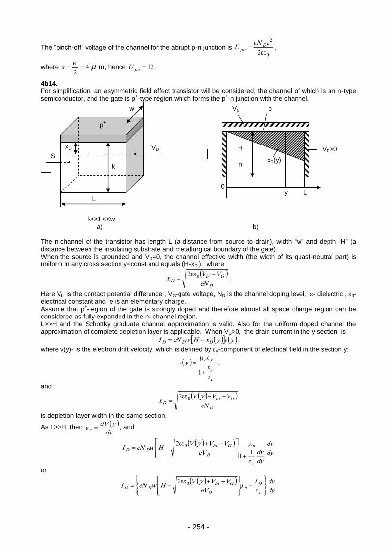
- 254 -
The “pinch-off” voltage of the channel for the abrupt p-n junction is 0
2
2εε
ε aNU D
po ,
where 42
wa m, hence 12poU .
4b14. For simplification, an asymmetric field effect transistor will be considered, the channel of which is an n-type semiconductor, and the gate is p
+-type region which forms the p
+-n junction with the channel.
k<<L<<w a) b) The n-channel of the transistor has length L (a distance from source to drain), width “w” and depth “H” (a distance between the insulating substrate and metallurgical boundary of the gate). When the source is grounded and VD=0, the channel effective width (the width of its quasI-neutral part) is uniform in any cross section y=const and equals (H-xD ), where
D
GbiD
eN
VVx
02εε
.
Here Vbi is the contact potential difference , VG-gate voltage, ND is the channel doping level, - dielectric , 0-electrical constant and e is an elementary charge. Assume that p
+-region of the gate is strongly doped and therefore almost all space charge region can be
considered as fully expanded in the n- channel region. L>>H and the Schottky graduate channel approximation is valid. Also for the uniform doped channel the approximation of complete depletion layer is applicable. When VD>0, the drain current in the y section is
yvyxHweNI DDD ,
where v(y)- is the electron drift velocity, which is defined by y-component of electrical field in the section y:
c
y
ynyv
ε
ε
εμ
1
,
and
D
GbiD
eN
VVyVx
02εε
is depletion layer width in the same section.
As L>>H, then
dy
ydVy ε , and
dy
dv
dy
dveV
VVyVHweNI
c
n
D
GbiDD
ε
μεε
11
2 0
or
dy
dvI
eV
VVyVHweNI
c
Dn
D
GbiDD
εμ
εε02
VG p+
VD>0
n xD(y)
0
y
L
H
L
k
w
p+
xD VD
S
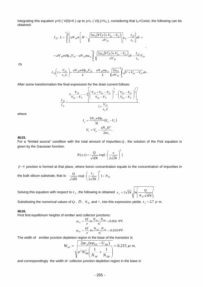
- 255 -
Integrating this equation y=0 ( V(0)=0 ) up to y=L ( V(L)=VD ), considering that ID=Const, the following can be obtained:
D
c
D
V
D
GbinDDnD
V
c
Dn
D
GbiDD
VI
dveV
VVyVweNVwHeN
dvI
eV
VVyVHweNLI
D
D
ε
εεμμ
εμ
εε
0
0
0
0
2
2
,
Or
DV
GbiD
nDDnD
c
DD dvVVV
eNL
weN
L
VwHeN
L
VI
0
021
εεμμ
ε.
After some transformation the final expression for the drain current follows:
L
V
VV
VV
VV
VVV
VV
V
I
I
c
D
Tbi
Gbi
Tbi
GbiD
Tbi
D
p
D
ε
1
232
3
2
3
,
where
Tbi
nD
pVV
L
wHNI
3
μ3
0
2
εε2
HeNVV D
biT .
4b15. For a “limited source” condition with the total amount of impurities Q , the solution of the Fick equation is
given by the Gaussian function.
]2
exp[),(
2
Dt
x
Dt
QtxN
np junction is formed at that place, where boron concentration equals to the concentration of impurities in
the bulk silicon substrate, that is: D
jN
Dt
x
Dt
Q
]
2exp[
2
Solving this equation with respect to jx , the following is obtained
DtN
QDtx
D
j
ln2
Substituting the numerical values of Q , D , DN and t , into this expression yields 7,2jx m.
4b16. First find equilibrium heights of emitter and collector junctions:
856020
.n
NNln
e
kT
i
DBAE
E
eV,
635020
.n
NNln
e
kT
i
AKDB
K
eV.
The width of emitter junction depletion region in the base of the transistor is
215.011
)(2
22
00
DBAE
DB
EBE
nE
NNNe
UeW
m,
and correspondingly the width of collector junction depletion region in the base is
- 256 -
258.011
)(2
22
00
DBAK
DB
BKK
nK
NNNe
UeW
m.
Therefore the width of the neutral base will be the following:
527.0 nKnEB WWWW m.
The concentration of minority carries (holes) at the emitter-base junction will equal the following:
12
2
101850
.
kT
eUexp
N
n)(p EB
DB
i
n
3cm .
Finally, the total charge of minority carries accumulated in the base is
1310462
0 .W)(peS
Q Bn K .
4b17. Bipolar diffusion coefficient is determined as
npD
p
D
n
pnD
.
For intrinsic semiconductor
pn
pn
DD
DDD
2.
Using Einstein relations one obtains
720μμ
μμ2,
e
TkD
pn
pnB
cm2/s.
4b18. First a density of donors in the semiconductor can be defined:
1510611
.e
Nn
Dρμ
3cm .
The built-in potential barrier for the electrons is equal to
GeAum ,
Here the semiconductor work function can be represented as
02
χχχχ g
GeD
i
i
cGe
D
cGeFcGeGe
E
N
nlnkT
n
NlnkT
N
NlnkTEE
where it is meant, that
,n
NlnkT
E
i
cg
2
and
1100 .n
NlnkT
i
D eV
Therefore, 224.Ge eV, and 78.0m eV.
4b19.
a) 996700103
3.
.II
Iγ
enep
ep
,
b) 996703
992.
.
I
Iα
ep
cpT ,
c) 993400 .γαα T
013.III enepe m²
99120010992 ...III cncpc mA
870000866001399340991200 .....IαII eccµ uA.
- 257 -
4b20.
2
7-
ox
oxF/cm.
cmcm105
F..
dC 7
14
10961085893ε
111096
1051061980ψ
7
1119
..
..
C
QV
ox
ox
SFB
V
0201096
84010106110858911284011
7
171914
.*.
......V
T
V
The substrate accumulation charge (Boron) will lead to flat-band bias by
oxC
qN bor, and therefore
ox
bor
C
qN02.06.0
12
19
7
bor 1067.2106.1
109.662.0N
cm-2
4b21.
2
1
22
21
kT
E
o
kT
E
o
e
e
σσ
σσ
1801181121
1
12
12
11
2
2
22
1
22021
..e
e
ee
ee
TTk
E
kT
E
kT
E
kT
E
kT
E
kT
E
σ
σ
σσσσ
Answer: will increase by 18%. 4b22.
pi
n
pn
n
neen
epen
μμσ
μμσ
2
n
np i
2
Find the minimum value from 0dn
dσ condition:
p
ni
n
pi
ii
n
pip
in
pi
n
n
n
n
n
np
nnn
n
n
nee
dn
d
μ
μ
μ
μ
μ
μμμ
μμσ
22
2
2
2
2
0
4b23.
m
kT
m
kT
e
kTL
e
kTD;DL;
m
e
d
d
ττ
μτ
μττ
μ
2
ox
BaSBFBT
C
)(qNVV
ψεψ
222
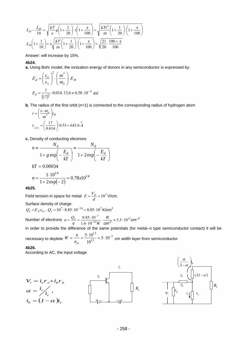
- 258 -
100
100
20
21
1001
20
11
10
11
1001
20
11
1001
20
11
10
2
xx
m
kTL
x
m
kTx
e
kTLL
D
DD
τ
ττμ
Answer: will increase by 15%.
4b24. a. Using Bohr model, the ionization energy of donors in any semiconductor is expressed by:
Ho
*
s
od E
m
mE
2
ε
ε
4
2105866130140
17
1 ...Ed eV
b. The radius of the first orbit (n=1) is connected to the corresponding radius of hydrogen atom
o
H*o
A...
r
rm
mr
bSnI6643530
0140
17
ε
c. Density of conducting electrons
14
14
1078.02exp21
101
00034.0
exp21exp1
xn
kT
kT
E
N
kT
Eg
Nn
d
d
d
d
4b25.
Field tension in space for metal 710d
VE k V/cm.
Surface density of charge 7147 108581085810 ..Q,EQ soks ε K/cm
2
Number of electrons 2-
2cm
cm
K
K
12
19
7
10551061
10858
..
.
q
Qn s
in order to provide the difference of the same potentials (for metal–n type semiconductor contact) it will be
necessary to deplete 3
15
12
10510
105
ssn
nW cm width layer from semiconductor.
4b26. According to AC, the input voltage
eb
e
c
bbeei
i1i
,i
i
ririV
bi
ci
LR
bi
ei gr br
LR
iV er
1rc
bi1
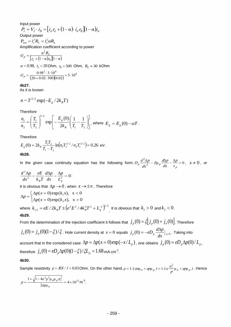
- 259 -
Input power
ebeeebii iririiVP αα 11
Output power
L
2
eL
2
cout RiRiP
Amplification coefficient according to power
αα
α
11
2
be
Lp
rr
RG
20,98.0 er Ohm, 500br Ohm, 30LR kOhm
4
42
10502050002020
103980
..
.G p
4b27. As it is known
)2/exp(~ 2/3 TkETn Bg
Therefore
21
2/3
2
1
2
1 11
2
)0(exp
TTk
E
T
T
n
n
B
g
, where
TEE gg )0( .
Therefore
26.0/ln2)0( 2/3
12
2/3
21
21
21
TnTnTT
TTkE Bg eV.
4b28.
In the given case continuity equation has the following form: 02
2
ppp
p
dx
pdE
dx
pdD
τμ , 0x , or
022
2
pB L
p
dx
pd
Tk
eE
dx
pd:
It is obvious that 0p , when x . Therefore
0 x),exp()0(
0 x),exp()0(
2
1
xkxp
xkxpp
where 2/122222
2,1 4/2/ pBB LTkEeTkeEk. It is obvious that 01 k and 02 k .
4b29.
From the determination of the injection coefficient it follows that )0()0()0( npp jjj . Therefore
/)1)(0()0( pn jj . Hole current density at 0x equals 0)0(
xpp
dx
pdeDj . Taking into
account that in the considered case )/exp()0( pLxxpp , one obtains ppp LpeDj /)0()0( ,
therefore 68.1/)1)(0()0( ppn LpeDj mA.cm-2
.
4b30.
Sample resistivity 030.l/RS ρ Ohm. On the other hand, )epp
ne/()epen/( pn
ipn μμμμρ
2
11 . Hence
21
222
1042
411
n
ipn
e
nep
ρμ
μμρm
-3.
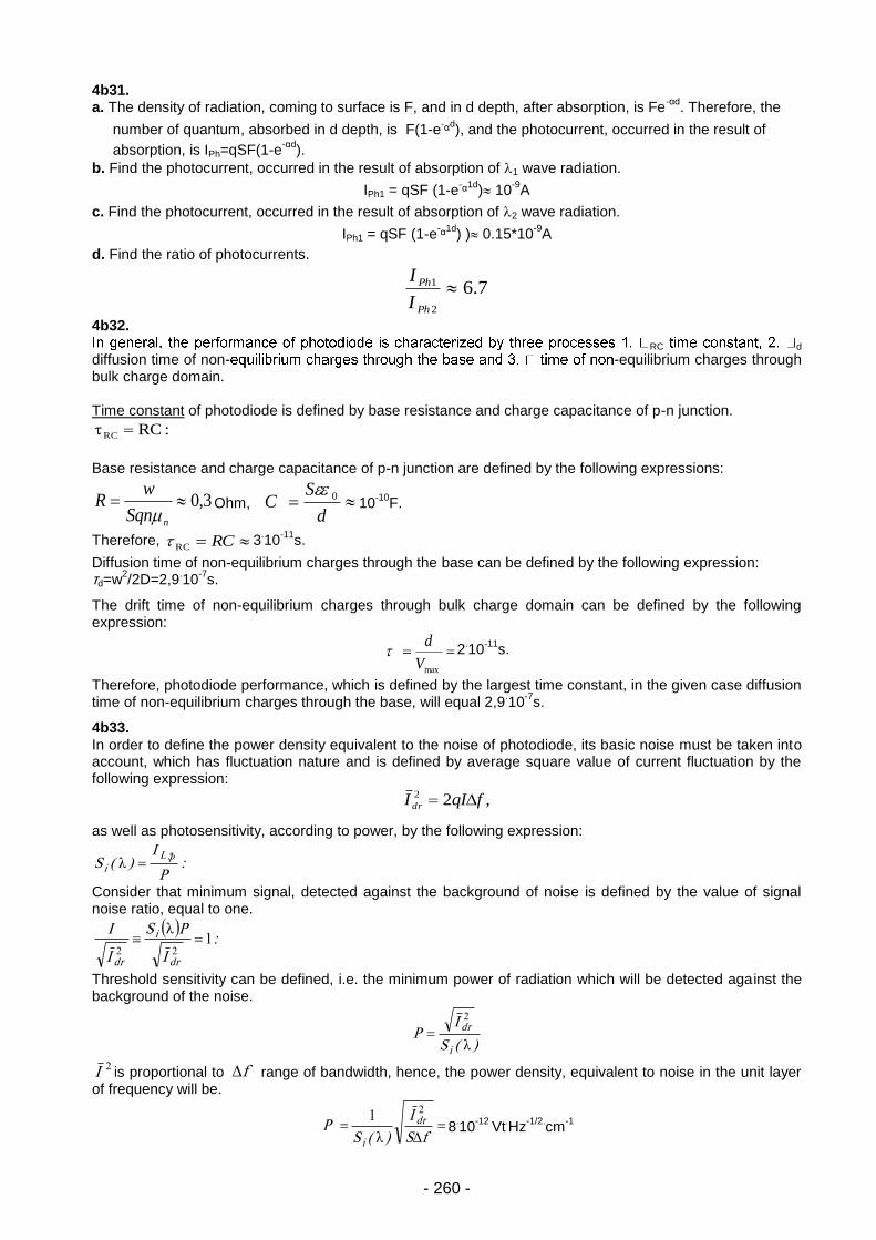
- 260 -
4b31. a. The density of radiation, coming to surface is F, and in d depth, after absorption, is Fe
-αd. Therefore, the
number of quantum, absorbed in d depth, is F(1-e-αd
), and the photocurrent, occurred in the result of
absorption, is IPh=qSF(1-e-αd
).
b. Find the photocurrent, occurred in the result of absorption of 1 wave radiation.
IPh1 = qSF (1-e-α1d
) 10-9
A
c. Find the photocurrent, occurred in the result of absorption of 2 wave radiation.
IPh1 = qSF (1-e-α1d
) ) 0.15*10-9
A
d. Find the ratio of photocurrents.
4b32.
RC d diffusion time of non- -equilibrium charges through bulk charge domain. Time constant of photodiode is defined by base resistance and charge capacitance of p-n junction.
:RCRC
Base resistance and charge capacitance of p-n junction are defined by the following expressions:
3,0nSqn
wR
Ohm,
d
SC 0
10-10
F.
Therefore, RCRC 3.10
-11s.
Diffusion time of non-equilibrium charges through the base can be defined by the following expression: τd=w
2/2D=2,9
.10
-7s.
The drift time of non-equilibrium charges through bulk charge domain can be defined by the following expression:
maxV
d 2
.10
-11s.
Therefore, photodiode performance, which is defined by the largest time constant, in the given case diffusion time of non-equilibrium charges through the base, will equal 2,9
.10
-7s.
4b33. In order to define the power density equivalent to the noise of photodiode, its basic noise must be taken into account, which has fluctuation nature and is defined by average square value of current fluctuation by the following expression:
,22 fqII dr
as well as photosensitivity, according to power, by the following expression:
:P
I)(S
ýL
i λ
Consider that minimum signal, detected against the background of noise is defined by the value of signal noise ratio, equal to one.
:
I
PS
I
I
dr
i
dr
122
λ
Threshold sensitivity can be defined, i.e. the minimum power of radiation which will be detected against the background of the noise.
)(S
IP
i
dr
λ
2
2I is proportional to f range of bandwidth, hence, the power density, equivalent to noise in the unit layer of frequency will be.
fS
I
)(SP dr
i
21
λ8
.10
-12 Vt
.Hz
-1/2.cm
-1
7.62
1 Ph
Ph
I
I
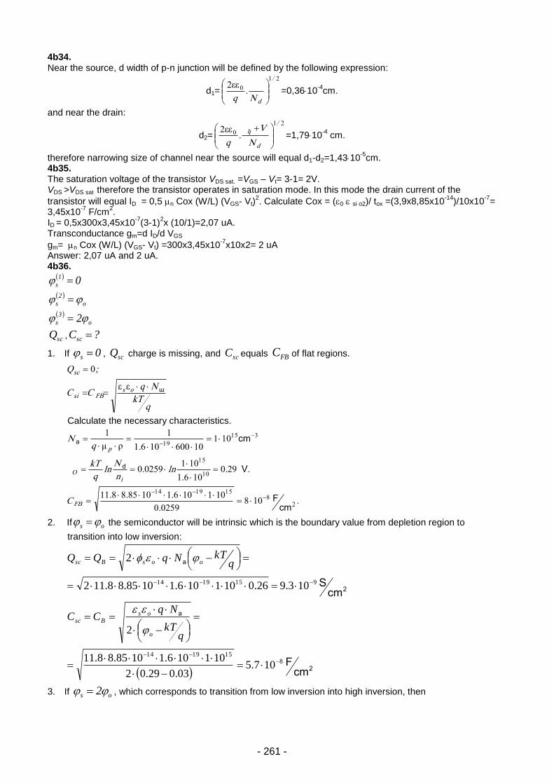
- 261 -
4b34. Near the source, d width of p-n junction will be defined by the following expression:
d1=
21
02/
dN.
q
εε=0,3610
-4cm.
and near the drain:
d2=
21
02/
d
Ï
N
V.
q
εε=1,7910
-4 cm.
therefore narrowing size of channel near the source will equal d1-d2=1,4310-5
cm. 4b35. The saturation voltage of the transistor VDS sat. =VGS – Vt= 3-1= 2V. VDS >VDS sat therefore the transistor operates in saturation mode. In this mode the drain current of the
transistor will equal ID = 0,5 n Cox (W/L) (VGS- Vt)2. Calculate Cox = (0 si o2)/ tox =(3,9x8,85x10
-14)/10x10
-7=
3,45x10⁻⁷
F/cm2.
ID = 0,5x300x3,45x10-7
(3-1)2x (10/1)=2,07 uA.
Transconductance gm=d ID/d VGS
gm= n Cox (W/L) (VGS- Vt) =300x3,45x10-7
x10x2= 2 uA Answer: 2,07 uA and 2 uA. 4b36.
o
3
s
o
2
s
1
s
2
0
scQ , ?Csc
1. If 0s , scQ charge is missing, and scC equals FBC of flat regions.
qkT
NqCC
;Q
osFBsi
sc
³
εε
0
Calculate the necessary characteristics.
..
...C
...
ln.n
Nln
q
kT
.qN
FB
iO
p
28
151914
10
15
315
19
10802590
101106110858811
2901061
10102590
101106001061
11
cmF
V
cm
d
a
ρμ
2. If os the semiconductor will be intrinsic which is the boundary value from depletion region to
transition into low inversion:
2
a
2
a
cmF
cmS
8151914
9151914
107.503.029.02
101106.11085.88.11
2
103.926.0101106.11085.88.112
2
qkT
NqCC
qkTNqQQ
o
osBsc
oosBsc
3. If os 2 , which corresponds to transition from low inversion into high inversion, then
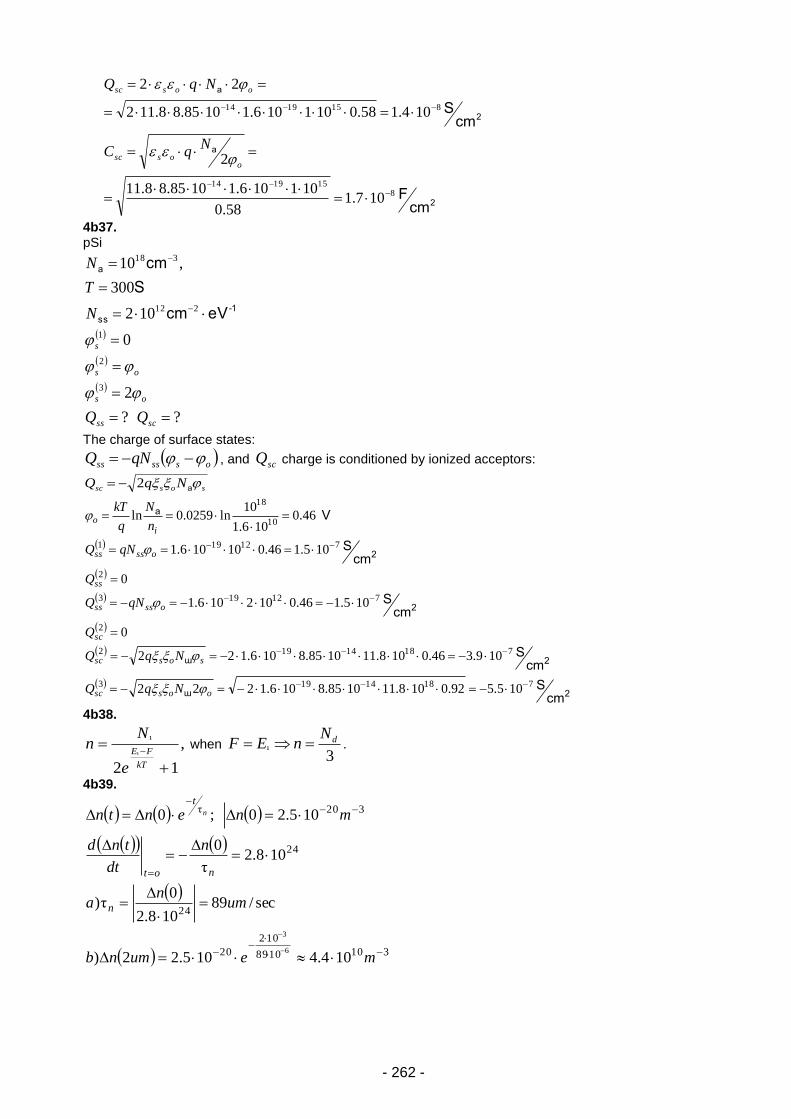
- 262 -
2
a
2
a
cmF
cmS
8151914
8151914
107.158.0
101106.11085.88.11
2
104.158.0101106.11085.88.112
22
oossc
oossc
NqC
NqQ
4b37. pSi
??
2
0
102
300
,10
3
2
1
212
318
scss
os
os
s
N
T
N
1-
ss
a
eVcm
S
cm
The charge of surface states:
osssss qNQ , and scQ charge is conditioned by ionized acceptors:
sossc NqQ a2
2³
2³
2
2
a
cmS
cmS
cmS
cmS
V
71814193
71814192
2
712193
2
712191
10
18
105.592.0108.111085.8106.1222
109.346.0108.111085.8106.122
0
105.146.0102106.1
0
105.146.010106.1
46.0106.1
10ln0259.0ln
oossc
sossc
sc
ossss
ss
ossss
io
NqQ
NqQ
Q
qNQ
Q
qNQ
n
N
q
kT
4b38.
,
12¹
¹
kT
FE
e
Nn when
3¹
dNnEF .
4b39.
3101089
102
20
24
24
320τ
104.4105.22)
sec/89108.2
0τ)
108.2τ
0
105.20;0
6
3
meumnb
umn
a
n
dt
tnd
mnentn
n
not
tn
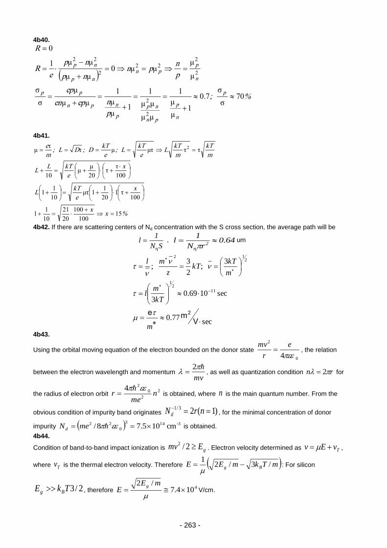
- 263 -
4b40.
%;.
p
nepen
ep
p
npn
np
np
eR
R
p
n
p
pn
np
p
npn
pp
n
ppn
np
np
7070
1
11
1
1
01
0
2
2
2
222
2
22
σ
σ
μ
μ
μμ
μμ
μ
μμμ
μ
σ
σ
μ
μμμ
μμ
μμ
4b41.
%xx
x
e
kTL
x
e
kTLL
m
kT
m
kTL
e
kTL;
e
kTD;DL;
m
e
15100
100
20
21
10
11
1001
20
11
10
11
1002010
2
τμτ
ττ
μμ
ττμτμττ
μ
4b42. If there are scattering centers of Nd concentration with the S cross section, the average path will be
SN
1l
¹
, 64.0rN
1l
2
¹um
sec77.0
sec1069.03
3;
2
3;
112
1
212
Vme 2
m
kT
ml
m
kTkT
z
ml
4b43.
Using the orbital moving equation of the electron bounded on the donor state
0
2
4
e
r
mv , the relation
between the electron wavelength and momentum mv
2 , as well as quantization condition rn 2 for
the radius of electron orbit 2
2
0
24n
mer
is obtained, where n is the main quantum number. From the
obvious condition of impurity band originates )1(23/1 nrNd , for the minimal concentration of donor
impurity -3143
0
22 cm 105.78/ meNd is obtained.
4b44.
Condition of band-to-band impact ionization is gEmv 2/2. Electron velocity determined as TvEv ,
where Tv is the thermal electron velocity. Therefore mTkmEE Bg /3/21
: For silicon
2/3TkE Bg , therefore 4104.7
/2
mEE
gV/cm.
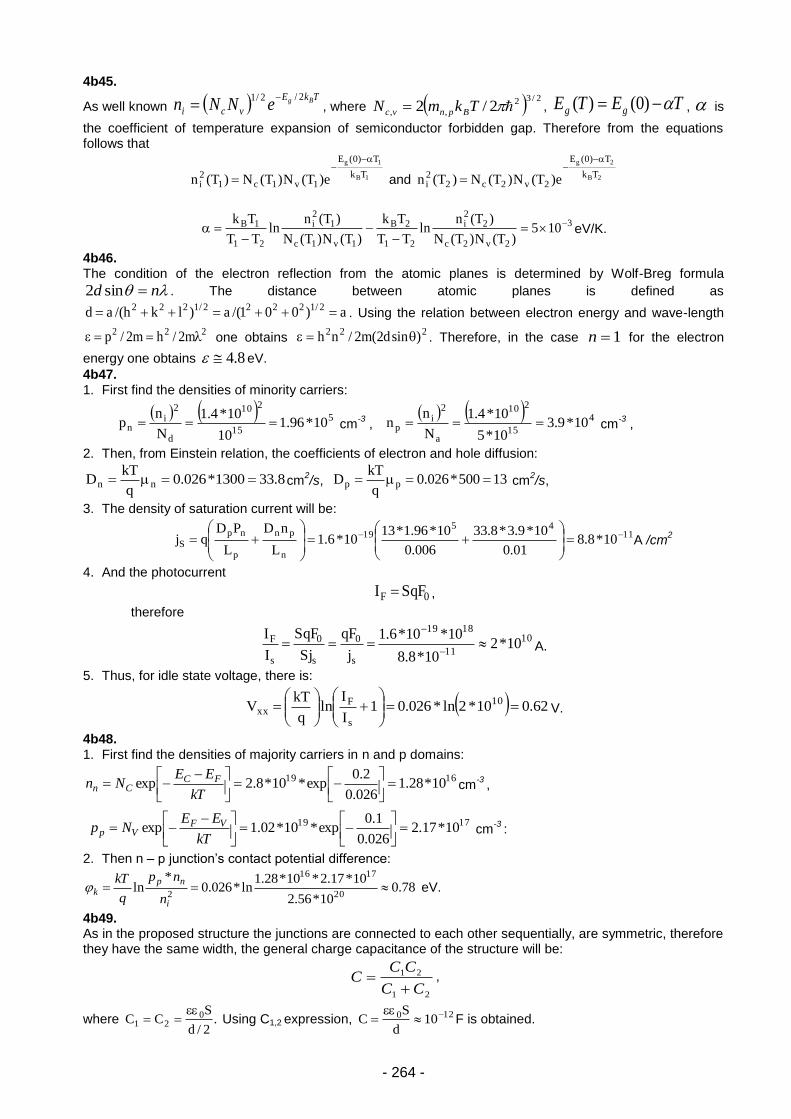
- 264 -
4b45.
As well known TkE
vciBgeNNn
2/2/1 , where 2/32
,, 2/2 TkmN Bpnvc , TETE gg )0()( , is
the coefficient of temperature expansion of semiconductor forbidden gap. Therefore from the equations follows that
1B
1g
Tk
T)0(E
1v1c12i e)T(N)T(N)T(n
and 2B
2g
Tk
T)0(E
2v2c22i e)T(N)T(N)T(n
3
2v2c
22i
21
2B
1v1c
12i
21
1B 105)T(N)T(N
)T(nln
TT
Tk
)T(N)T(N
)T(nln
TT
Tk
eV/K.
4b46. The condition of the electron reflection from the atomic planes is determined by Wolf-Breg formula
nd sin2 . The distance between atomic planes is defined as
a)001/(a)lkh/(ad 2/12222/1222 . Using the relation between electron energy and wave-length
222 m2/hm2/p one obtains 222 )sind2(m2/nh . Therefore, in the case 1n for the electron
energy one obtains 8.4 eV.
4b47. 1. First find the densities of minority carriers:
5
15
210
d
2i
n 10*96.110
10*4.1
N
np cm
-3 ,
4
15
210
a
2i
p 10*9.310*5
10*4.1
N
nn cm
-3 ,
2. Then, from Einstein relation, the coefficients of electron and hole diffusion:
8.331300*026.0q
kTD nn cm
2/s, 13500*026.0
q
kTD pp cm
2/s,
3. The density of saturation current will be:
11
4519
n
pn
p
np
S 10*8.801.0
10*9.3*8.33
006.0
10*96.1*1310*6.1
L
nD
L
PDqj
A /cm
2
4. And the photocurrent
0F SqFI ,
therefore
10
11
1819
s
0
s
0
s
F 10*210*8.8
10*10*6.1
j
qF
Sj
SqF
I
I
A.
5. Thus, for idle state voltage, there is:
62.010*2ln*026.01I
Iln
q
kTV 10
s
Fxx
V.
4b48. 1. First find the densities of majority carriers in n and p domains:
1619 10*28.1026.0
2.0exp*10*8.2exp
kT
EENn FC
Cn cm-3
,
1719 10*17.2
026.0
1.0exp*10*02.1exp
kT
EENp VF
Vp cm-3
:
2. Then n – p junction’s contact potential difference:
78.010*56.2
10*17.2*10*28.1ln*026.0
*ln
20
1716
2
i
npk
n
np
q
kT eV.
4b49. As in the proposed structure the junctions are connected to each other sequentially, are symmetric, therefore they have the same width, the general charge capacitance of the structure will be:
21
21
CC
CCC
,
where .2/d
SCC 0
21
Using C1,2 expression, 120 10
d
SC
F is obtained.
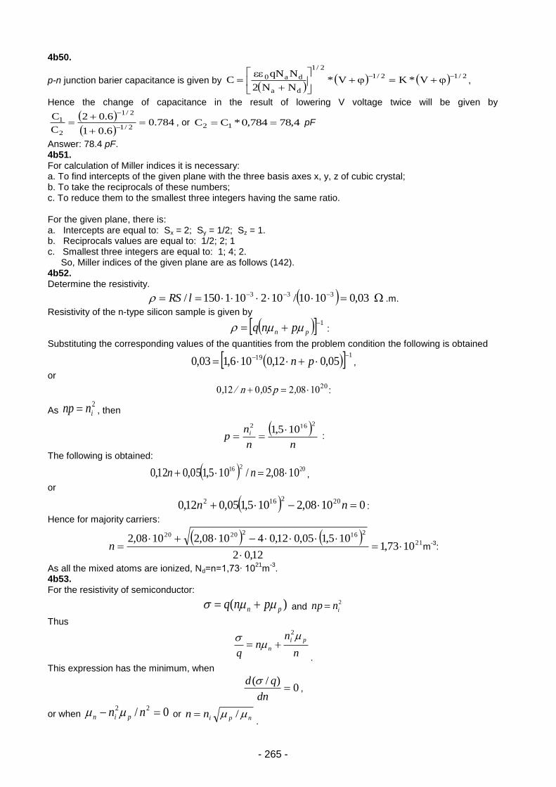
- 265 -
4b50.
p-n junction barier capacitance is given by
2/12/1
2/1
da
da0 V*KV*NN2
NqNC
,
Hence the change of capacitance in the result of lowering V voltage twice will be given by
784.06.01
6.02
C
C2/1
2/1
2
1
, or 4,78784,0*CC 12 pF
Answer: 78.4 pF. 4b51. For calculation of Miller indices it is necessary: a. To find intercepts of the given plane with the three basis axes x, y, z of cubic crystal; b. To take the reciprocals of these numbers; c. To reduce them to the smallest three integers having the same ratio. For the given plane, there is: a. Intercepts are equal to: Sx = 2; Sy = 1/2; Sz = 1. b. Reciprocals values are equal to: 1/2; 2; 1 c. Smallest three integers are equal to: 1; 4; 2.
So, Miller indices of the given plane are as follows (142). 4b52. Determine the resistivity.
03,01010/102101150/ 333 lRS .m.
Resistivity of the n-type silicon sample is given by
1 pn pnq :
Substituting the corresponding values of the quantities from the problem condition the following is obtained
119 05,012,0106,103,0 pn ,
or 2010082050120 ,p,n/, :
As 2
innp , then
nn
np i
2162105,1
:
The following is obtained:
20216 1008,2/105,105,012,0 nn ,
or
01008,2105,105,012,0 202162 nn :
Hence for majority carriers:
21
21622020
1073,112,02
105,105,012,041008,21008,2
n m
-3:
As all the mixed atoms are ionized, Nd=n=1,73∙ 1021
m-3
. 4b53. For the resistivity of semiconductor:
)( pn pnq and 2
innp
Thus
n
nn
q
pi
n
2
.
This expression has the minimum, when
0)/(
dn
qd ,
or when 0/ 22 nn pin or npinn /
.

- 266 -
Since 2
2 )/(
dn
qd the value of this expression is positive, then in this point pni
nn / resistivity has the
minimum value. 4b54.
For the p-type silicon ppp q . From this expression for the hole densities in the p-region, the following
is obtained: 23194 1029,3)106,119,0/(10)/(
ppp qp m-3
:
Similarly for the n-type silicon: 2119 106,1)106,139,0/(100)/(
nnn qn m-3
For the hole densities in the n-region: 17212192 1091,3)1060,1/()105,2(/ nin nnp m
-3
Therefore the built-in potential is equal to:
35,01091,3
1029,3ln
106,1
3001038,1ln
17
23
19
20
n
p
kp
p
q
kT V.
4b55. Let us find the diode DC current for the DC voltage (V=0,1V) by the following formula
17,1)1)3001038,1/1,0106,1(exp(1025)1exp( 23196
0
kT
qVII mA:
In this case DC resistance of diode is equal to
85)1017,1/(1,0/ 3
0 IVR .
4b56.
For wet oxidation at 9500C BtAdd
0
2
0
Rearranging the equation Ad
Btd
0
0
Thus, a plot of do versus t/do will give B as the slope and A as the intercept.
do (µm) 0.041 0.100 0.128 0.153 0.177
t/do (h/µm) 2.683 3.000 3.125 3.268 3.390
From the plot, the intercept of the line yields A = 0.50 µm. The slope of the line yields B = 0.2 µm
2h.
4b57. For a “limited source” condition with the total amount of impurities Q , the solution of Fick equation is given by
the Gaussian function.
]2
exp[),(
2
Dt
x
Dt
QtxN
np junction is formed at the place, where boron concentration equals the concentration of impurities in the
bulk silicon substrate, that is:
D
jN
Dt
x
Dt
Q
]
2exp[
2
Solving this equation with respect to jx ,
DtN
QDtx
D
j
ln2
Substituting the numerical values of Q , D , DN and t , into this expression yields
7,2jx m.
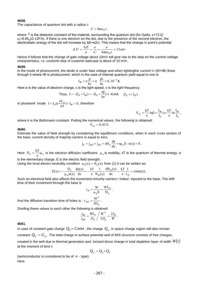
- 267 -
4b58. The capacitance of quantum dot with a radius r:
rC 04πεε ,
where is the dielectric constant of the material, surrounding the quantum dot (for GaAs, ε=13.2) ε0=8.85g10-12F/m. If there is one electron on the dot, due to the presence of the second electron, the electrostatic energy of the dot will increase by ΔE=e2/c. This means that the change in point’s potential
mvr
e
C
e
e
EV 11
4 0
πεε
Hence it follows that the change of gate voltage about 10mV will give rise to the step on the current-voltage characteristics, i.e. coulomb step of coulomb staircase is about of 10 mVr.
4b59. In the mode of photocurrent, the diode is under bias voltage and when lightingthe current I=-(I0+IΦ) flows through it where IΦ is photocurrent, which in the case of internal quantum yield equal to one is
3Φ 106
hc
pλe
hν
peI A.
Here e is the value of electron charge, c is the light speed, ν is the light frequency.
Thus, -6)hν
ep(I -)II(I 0Φ0 mA )II( Φ0 .
In photoemf mode 0,I -)kT
eVe(II xx
0 therefore
00xx
I
Iln
e
kT)
I
I1ln(
e
kTV ,
where k is the Boltzmann constant. Putting the numerical values, the following is obtained:
35.0Vxx V.
4b60. Estimate the value of field strength by considering the equilibrium conditions, when in each cross section of the base, current density of majority carriers is equal to zero.
0)x(nEedx
dneDjjj nnnEnDn .
Here nne
kTD is the electron diffusion coefficient, nμ is mobility, кТ is the quantum of thermal energy, e
is the elementary charge, E is the electric field strength.
Using the local electro neutrality condition )x(N)x(n 00 from (1) it can be written as:
)y(constL
1
e
kT
dx
)x(dN
)x(N
1
e
kT
dx
)x(dn
)x(n
D)x(E
0
D
Dn
n
.
Such an electrical field also affects the movement minority carriers / holes/, injected to the base. The drift time of their movement through the base is
p
0
pdr
D
WL
E
Wt
.
And the diffusion transition time of holes is : p
2
difD2
Wt .
Dividing these values to each other the following is obtained:
W
L
D
W
D
WL
t
t
pp
02
0 2
2
dif
dr .
4b61.
In case of constant gate charge ConstQG , the charge scQ in space charge region will also remain
constant scG GQ . The total charge in surface potential well of MIS structure consists of free charges,
created in the well due to thermal generation and ionized donor charge in total depletion layer of width tW
at the moment of time t:
dpsc QQQ
(semiconductor is considered to be of n - type).
Here
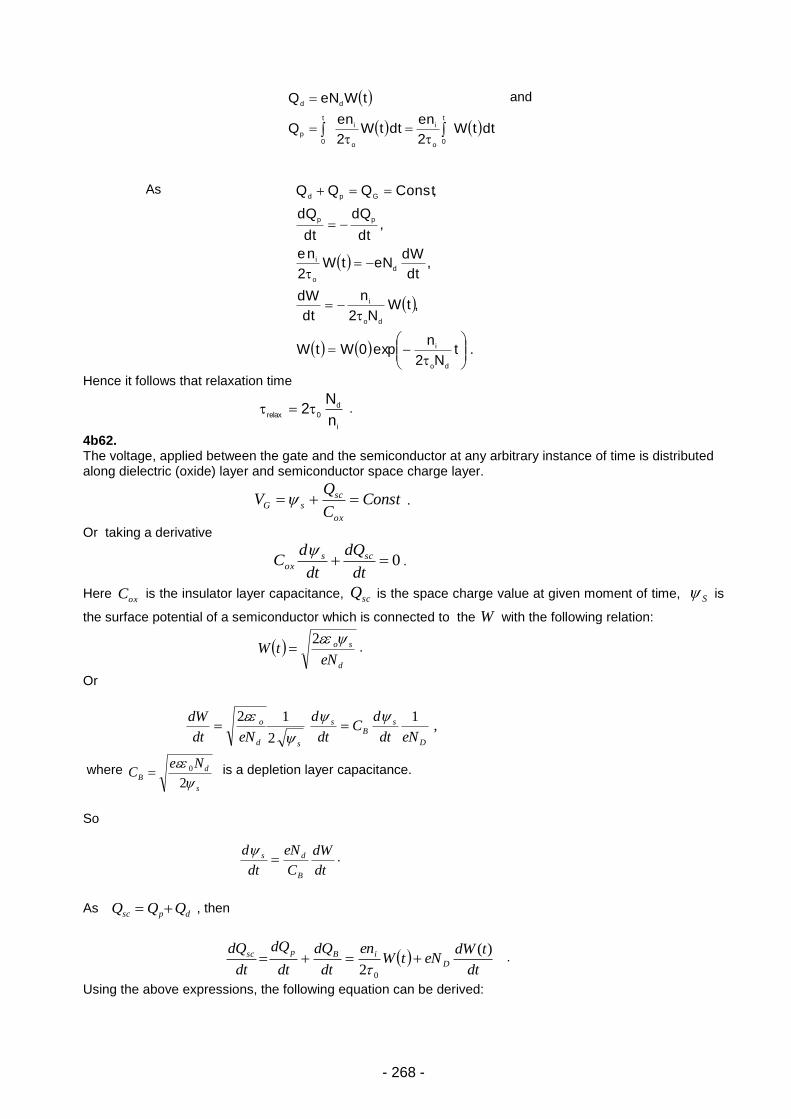
- 268 -
and
As
Hence it follows that relaxation time
i
d
0relaxn
N2 .
4b62. The voltage, applied between the gate and the semiconductor at any arbitrary instance of time is distributed along dielectric (oxide) layer and semiconductor space charge layer.
ConstC
QV
ox
scsG .
Or taking a derivative
0dt
dQ
dt
dC scs
ox
.
Here oxC is the insulator layer capacitance, scQ is the space charge value at given moment of time, S is
the surface potential of a semiconductor which is connected to the W with the following relation:
d
so
eNtW
2 .
Or
,1
2
12
D
sB
s
sd
o
eNdt
dC
dt
d
eNdt
dW
where
s
dB
NeC
2
0 is a depletion layer capacitance.
So
dt
dW
C
eN
dt
d
B
ds
.
As dpsc QQQ , then
dt
tdWeNtW
en
dt
dQ
dt
dQ
dt
dQD
iBpsc )(
2 0
.
Using the above expressions, the following equation can be derived:
dttW2
endttW
2
enQ
tWeNQ
t
0o
i
o
it
0p
dd
.tN2
nexp0WtW
,tWN2
n
dt
dW
,dt
dWeNtW
2
ne
,dt
dQ
dt
dQ
,ConstQQQ
do
i
do
i
d
o
i
pp
Gpd
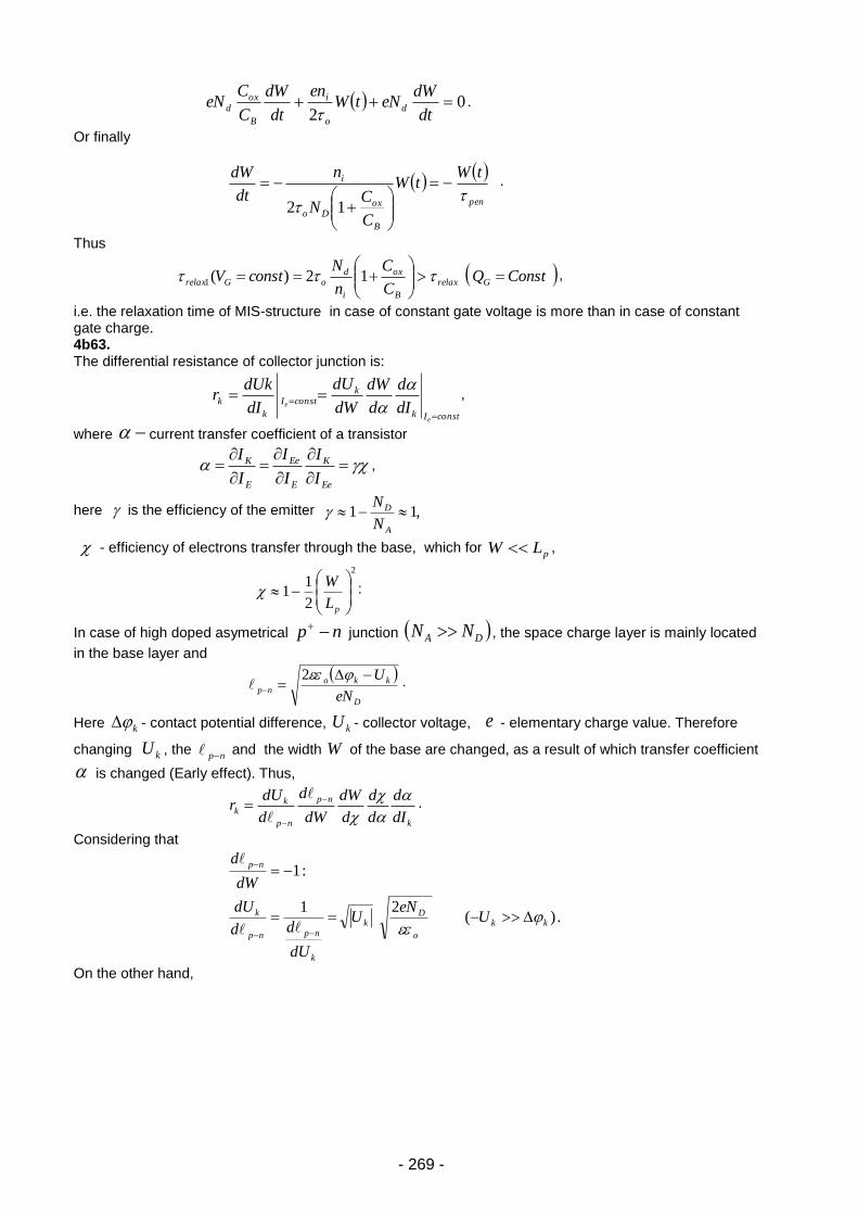
- 269 -
02
dt
dWeNtW
en
dt
dW
C
CeN d
o
i
B
oxd
.
Or finally
pen
B
oxDo
i tWtW
C
CN
n
dt
dW
12
.
Thus
ConstQC
C
n
NconstV Grelax
B
ox
i
doGrelax
12)(1
,
i.e. the relaxation time of MIS-structure in case of constant gate voltage is more than in case of constant gate charge. 4b63. The differential resistance of collector junction is:
constIk
kconstI
k
k
e
e dI
d
d
dW
dW
dU
dI
dUkr
,
where current transfer coefficient of a transistor
Ee
K
E
Ee
E
K
I
I
I
I
I
I,
here is the efficiency of the emitter ,11 A
D
N
N
- efficiency of electrons transfer through the base, which for pLW ,
2
2
11
pL
W :
In case of high doped asymetrical np junction DA NN , the space charge layer is mainly located
in the base layer and
D
kkonp
eN
U
2 .
Here k - contact potential difference, kU - collector voltage, e - elementary charge value. Therefore
changing kU , the np and the width W of the base are changed, as a result of which transfer coefficient
is changed (Early effect). Thus,
k
np
np
kk
dI
d
d
d
d
dW
dW
d
d
dUr
.
Considering that
UeN
U
dU
dd
dU
dW
d
kk
o
Dk
k
npnp
k
np
.)(21
:1
On the other hand,
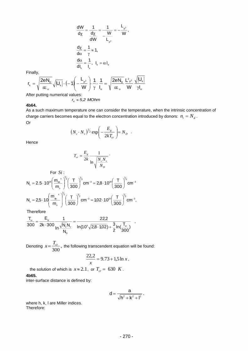
- 270 -
ek
ek
p
p
II,I
1
dI
d
,11
d
d
,W
L
L
W
1
dW
d
1
d
dW 2
2
Finally,
e
kp2
o
D
e
p
k
o
D
kI
U
W
LeN2
I
11
W
L1U
eN2r
22
After putting numerical values: MOhm2,5rk
4b64. As a such maximum temperature one can consider the temperature, when the intrinsic concentration of
charge carriers becomes equal to the electron concentration introduced by donors: di Nn .
Or
D
cr
g
vc NkT
ENN
2exp2
1 .
Hence
D
vc
g
cr
N
NNk
ET
ln
1
2 .
For Si :
,
)300
Tln(
2
3)02,18,210ln(
2,22
N
NNln
1
300k2
E
300
T
Therefore
,300
T1002,1
300
T
m
m105,2N
300
T108,2
300
T
m
m105.2N
cr4
D
vc
gcr
32
3
1932
323
o
x
dp
v
32
3
1932
323
o
x
dn19
c
cmcm
cmcm
Denoting ,300
crTx the following transcendent equation will be found:
xx
ln5,173.92,22
,
the solution of which is 1.2x , or KTcr 630 .
4b65. inter-surface distance is defined by:
222 lkh
ad
,
where h, k, l are Miller indices. Therefore:
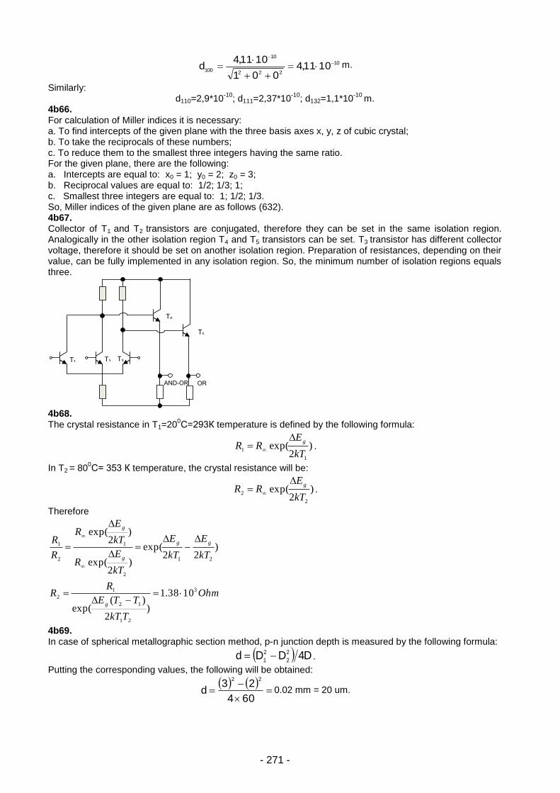
- 271 -
10
222
10
1001011,4
001
1011,4d
m.
Similarly: d110=2,9*10
-10; d111=2,37*10
-10; d132=1,1*10
-10 m.
4b66. For calculation of Miller indices it is necessary: a. To find intercepts of the given plane with the three basis axes x, y, z of cubic crystal; b. To take the reciprocals of these numbers; c. To reduce them to the smallest three integers having the same ratio. For the given plane, there are the following: a. Intercepts are equal to: x0 = 1; y0 = 2; z0 = 3; b. Reciprocal values are equal to: 1/2; 1/3; 1; c. Smallest three integers are equal to: 1; 1/2; 1/3. So, Miller indices of the given plane are as follows (632). 4b67. Collector of T1 and T2 transistors are conjugated, therefore they can be set in the same isolation region. Analogically in the other isolation region T4 and T5 transistors can be set. T3 transistor has different collector voltage, therefore it should be set on another isolation region. Preparation of resistances, depending on their value, can be fully implemented in any isolation region. So, the minimum number of isolation regions equals three.
4b68. The crystal resistance in T1=20
0C=293К temperature is defined by the following formula:
)2
exp(1
1kT
ERR
g
.
In T2 = 800C= 353 К temperature, the crystal resistance will be:
)2
exp(2
2kT
ERR
g
.
Therefore
Ohm
TkT
TTE
RR
kT
E
kT
E
kT
ER
kT
ER
R
R
g
gg
g
g
3
21
12
1
2
21
2
1
2
1
1038.1
)2
)(exp(
)22
exp(
)2
exp(
)2
exp(
4b69. In case of spherical metallographic section method, p-n junction depth is measured by the following formula:
D4DDd 2
2
2
1 .
Putting the corresponding values, the following will be obtained:
604
23d
22
0.02 mm = 20 um.
AND-OR OR
T1 T2 T3
T4
T5
- 272 -
4b70. Symbols of plane passing through points A,B and C can be determined by solving the system of three equations of the following type 1lzkyhx . The result obtained is )111()hkl( . The angle between the
crystalline planes )111( and (121) can be determined using the scalar product of vectors perpendicular to
the planes: 18/4cos .
4b71. At temperature T=0K Fermi energy F is determined though conduction electron concentration n as
3/22
2
)n3(m2
F
. In face-centred cubic crystal the concentration of atoms equals 3
atoma/4n . Therefore
3.312
a)/mF2(n/n
2
3
2/32
atom
.
4b72.
Continuity equation Rdt
nd
for electrons can be presented in form )pp)(nn(
dt
nd00n
,
where 0n and 0p are the equilibrium and n and p non-equilibrium concentrations of electrons and
holes, correspondingly. As well 2
i00npn , pn then )nn)n(
dt
nd0
2
n
. Solving the diff-
equation with st
n)0t(n initial condition one obtained
st
tn
st0
st0
ne)nn(
nn)t(n
0n
.
4b73.
From tsineEdt
xdm
02
2
Newton equation of electron in electromagnetic field tsinEE0
it follows that
electron displacement from the equilibrium state is determined as tsinm
eEx
2
0
. Therefore, for the
polarization, i.e. unit volume dipole momentum one has enm
tsineEenxP
2
0
. Using relation
E)1(EP0r0 , for dielectric permittivity one obtains )
m
en1(
2
0
2
0
.
4b74.
1. The ray absorption is performed by exponential law x
0eFF , where F is the intensiveness in x
depth, therefore 25,010ln10F
Fln
1x 116
1
0
1
um.
2. 375,0Fln10F
Fln
1x
0
6
2
0
2
um.
3. So, the active layer width d = x1 – x2 0,12 um.
4b75. 1. From the ray absorption law:
x
011
1eFxF , and x
0222eFxF
,
therefore
)(x
01
02
x
01
x
02
1
2 21
1
2
eF
F
eF
eF
xF
xF
.
2. In x1 point )(x
01
02
12
1211
211eFF
)x(F)x(F2)x(F .
- 273 -
From (1) 143.010ln1067,5)x(F
Fln
1x 117.
12
02
2
1
um.
3. From (2) )(x
0201
211eF2F , and 171,3)(x
211 ,
therefore 17.6,316.)(x
0201103,7e102eF2F 211
qv/cm
2.v.
4b76. It is known that the permittivity coefficient of rectangular potential barrier:
d)EE(m22
0
0
eDD
.
The permittivity coefficient of an electron:
16.2102.01.610109,12
1,054.10
2
0ee2.0eDD
9.-19-31..
34-
0.023
Proton permittivity coefficient:
216102.01.6101,67.102
1,054.10
2
0pe2.0eDD
9.-19-27.
34-
4.8.10
-19
4b77.
∆st stationary photoconductance:
∆st = q∆nst(n+ p)
At switching off the light, the density of nonequilibrium charge carriers decreases by the following law:
∆n = ∆nst
)( 1tt
e
Hence it follows that
∆st /2= q∆nst(n+p) /2 = ∆st
)( 12 tt
e
therefore
)tt( 12 = ln2, or t2 - t1 =
.ln2 = 0.69
.10
-6 v.
4b78.
The number of free places in the crystal with N atoms is: ;Nen kT
E
Free places per atom: kT
E
1e
N
nn
For T1 = 300oK
14300221038.1
19
106.175.0
11025en
For T2 = 600oK
7600221038.1
19
106.175.0
1105en
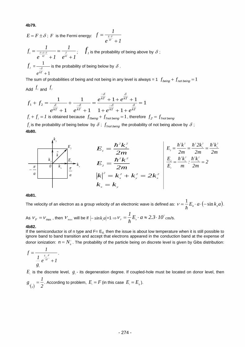
- 274 -
4b79.
FE ; F is the Fermi energy:
1e
1f
kT
FE
1e
1
1e
1f
kTkT
FF1
; 1
f is the probability of being above by ;
2f =
1
1
kTe
is the probability of being below by .
The sum of probabilities of being and not being in any level is always = 1 1 being notbeing ff
Add 1f
and 2f
1
11
11
1
1
1
121
kTkT
kTkT
kTkT ee
ee
ee
ff
1ff21 is obtained because 1 being 1not1being ff , therefore being 1not2 ff
2f is the probability of being below by ; being 1notf the probability of not being above by ;
4b80.
4b81.
The velocity of an electron as a group velocity of an electronic wave is defined as: akaE xo sin1
.
As max F , then max will be if aksin
x =1
7
oF103.2aE
1
cm/s.
4b82. If the semiconductor is of n type and F= Ed, then the issue is about low temperature when it is still possible to ignore band to band transition and accept that electrons appeared in the conduction band at the expense of
donor ionization: ¹
Nn . The probability of the particle being on discrete level is given by Gibs distribution:
1eg
1
1f
kT
iE
i
F -
.
iE is the discrete level,
ig - its degeneration degree. If coupled-hole must be located on donor level, then
2
1g
i
¹
. According to problem, FEi (in this case
¹EE
i ).
yx
2
x
2
y
2
x
2
22
2
2
x
2
1
kk
k2kkk
m2
kE
m2
kE
2m2
k:
m
k
E
E
m2
k
m2
k2
m2
kE
2
x
22
x
2
1
2
2
x
22
x
222
2
yk
yk
xk
xk 0
k
a
a
2E
1E
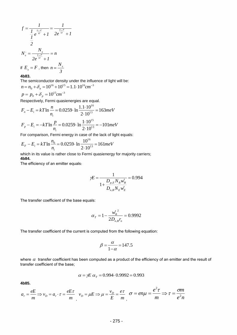
- 275 -
n1e2
NN
1e2
1
1e
2
1
1
1f
kT
E
kT
E
kT
E
F
¹
¹
FF
-¹-
-¹--¹-
if FE ¹
, then 3
Nn
¹
4b83. The semiconductor density under the influence of light will be:
3161516
0 101.11010 cmnn n 315
0 10 cmpp p Respectively, Fermi quasienergies are equal.
meVn
nkTEF
i
in 163102
101.1ln0259.0ln
13
16
meVn
pkTEF
i
ip 101102
101ln0259.0ln
13
15
For comparison, Fermi energy in case of the lack of light equals:
meVn
nkTEE
i
iF 161102
10ln0259.0ln
13
16
0
which in its value is rather close to Fermi quasienergy for majority carriers; 4b84.
The efficiency of an emitter equals:
994.0
1
1
,
,
EEBn
BBEp
wND
wNDE
The transfer coefficient of the base equals:
9992.02
1,
2
nBn
BT
rD
w
The transfer coefficient of the current is computed from the following equation:
5.1471
where transfer coefficient has been computed as a product of the efficiency of an emitter and the result of
transfer coefficient of the base;
993.09992.0994.0 TE
4b85.
m
eEav
m
eEa D
, m
e
E
vEv D
D
, ne
m
m
een
2
2
- 276 -
ne
m
m
een
2
2
,
mkTv
mvkT D
322
3 2
ne
mm
kTne
mvv DD 22
3
cm
seccm
1111
2
28
282
10511.38103.367.11
67.111011.9
3001038.13322
3
ne
mvv
mkTv
mvkT
DD
D
4b86.
It is known that b
NqC
20 0 , and
V
NqVC
b
2
0 £ . Therefore, their 0/ CVC ratio will be
VC
VC
b
b
0, and the respective curve will have the following form:
4b87. The width of depletion layer is defined by the following formula:
2/1
02
a
b
qN
Vw
, hence
0
2
2 a
b
NqwV £
Putting numerical values, the following will be obtained:
1. VNqw
V ab 59.0
10*86.8*12*2
10*10*5*10*9.16.0
2 14
101419
0
2
2. 45.010*86.8*12*2
10*2*10*5*10*9.16.0
2 14
101419
0
2
a
b
NqwV V
4b88. In homogeneous environment, F intensity of the ray depends on x depth of absorption by Buger - Lambert law.
xeFF 0 , where F0 – initial intensity, F – intensity in x depth, - absorption coefficient.
It is obvious that in x = 0.5 mkm depth, where the intensities of two waves equal each other, the following condition takes place:
xxeFFeFF 21
022011
, hence
1)(
01
02
01
02 12
1
2
x
x
x
eF
F
eF
eF,
hence )(
010212
x
eFF . Putting the value, the following will be obtained:
19.10210515)(0102 102.210
5..5.12
eeFF
x qv./cm
2.s.
V, ì
0/ CVC
0
1
2
3
4
5
6
7
0 0.1 0.2 0.3 0.4 0.5 0.6
- 277 -
4b89.
The length of drift of holes ppd EL .
Use diffusion length and Einstein relations:
2/1
ppp DL and qkTD pp // :
Putting the above equation in the expression of drift length, the following will be obtained:
kTqELL pd /2 0.09 cm.
4b90. The forward-bias current can be written as follows:
)/exp()/exp(~ TkeVTkEJ BBg .
Therefore, for a given temperatures the following will be obtained:
)/exp()/exp(
)/exp()/exp(/
111
222
22TkeVTkE
TkeVTkEJJ
BBg
BBg
.
If current is to remains constant, then 21 JJ and:
)/exp()/exp( 1122 TkeVETkeVE BgBg .
Then, V2 = 0.58 V is obtained. The change in the forward-bias voltage is 0.02 V. 4b91.
Average energy of electron is determined as kk dEfdEEfE )(/)( , where )(Ef is the Fermi-Dirac
distribution function. From the relation mkE 2/22 between the electron energy and momentum it
follows that the average energy of electron is dEEEfdEEEfE 2/12/3 )(/)( . Using the behavior of
the Fermi-Dirac function at 0T , for the electron average energy FdEEdEETE
F F
5
3/)0(
0 0
2/12/3
is obtained. At temperature T=0 K Fermi energy F is determined through n concentration of conduction
electron as 3/22
2
)3(2
nm
F
. Therefore 3/22
2
)3(10
3)0( n
mTE
.
4b92.
Solution of the continuity equation 02
2
PB L
p
dx
pd
Tk
eE
dx
pd is )exp()0( kxxpp , where
)/411(2/1 ELllk , eETkl B / , TkeELL BpE /2 . In the given case 1/ pLl . Therefore
ELk /1 and )/exp()0( ELxxpp .
4b93.
It is known that SJI xx , zyddS , xxpnx EEepenJ , xxx dEV . The Hall’s voltage
determined as zxHH BdJRV where 2
22
pn
np
Hpn
np
e
rR
is the Hall’s coefficient, r is the Hall’s factor
which is order of unit ( 1r ). Therefore for the Hall’s voltage there is
Bd
I
pn
np
eV
z
x
pn
np
H 2
221
. From
the 0HV condition of the problem it follows that semiconductor conductivity is n-type ( pn ). Then
Bd
I
enV
z
xH
1 or B
d
I
eVn
z
x
H
1 . Therefore electron conductivity and mobility can be calculated on the
base of relations xx JE / and enn /1 .
4b94.
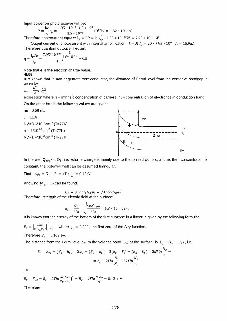
- 278 -
Input power on photoreceiver will be:
Therefore photocurrent equals:
Output current of photocurrent with internal amplification:
Therefore quantum output will equal:
⁄
‐
‐
Note that e is the electron charge value. 4b95. It is known that in non-degenrate semiconductor, the distance of Fermi level from the center of bandgap is given by
expression where ni – intrinsic concentration of carriers, n0 – concentration of electroncs in conduction band.
On the other hand, the following values are given:
mh= 0.56 m0
= 11.8
Nc*=3.6*1018
cm-3
(T=77K)
ni = 3*10-20
cm-3
(T=77K)
Nv*=1.4*1018
cm-3
(T=77K)
In the well Qfree << QB, i.e. volume charge is mainly due to the ionized donors, and as their concentration is
constant, the potential well can be assumed triangular.
Find
Knowing S , QВ can be found.
√ √
Therefore, strength of the electric field at the surface:
√
It is known that the energy of the bottom of the first subzone in a linear is given by the following formula:
[
( ) ]
, where
the first zero of the Airy function.
Therefore eV.
The distance from the Fermi level to the valence band at the surface is ( ) , i.e.
( ) ( ) ( ) ( )
i.e.
(
)
eV
Therefore
0ee
0 E1 E2
E
c EF
Ev
Ec
e
s
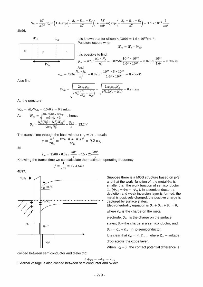
- 279 -
( (
))
(
)
4b96.
It is known that for silicon ( ) .
Puncture occurs when
It is possible to find:
And
Also find
√
( ) √
( )
At the puncture
‐ ‐
As √
( )
(
)
, hence
(
)
The transit time through the base without ( ) , equals
( )
,
as
Knowimg the transit time we can calculate the maximum operating frequency
4b97.
Suppose there is a MOS structure based on p-Si
and that the work function of the metal М is smaller than the work function of semiconductor
s ( ). In a semiconductor, a depletion and weak inversion layer is formed, the metal is positively charged, the positive charge is captured by surface states. Electroneutrality equation is ,
where is the charge on the metal
electrode, is the charge on the surface
states, – the charge in a semiconductor, and
in p-semiconductor.
It is clear that , where voltage
drop across the oxide layer.
When 0, the contact potential difference is
divided between semiconductor and dielectric:
External voltage is also divided between semiconductor and oxide:
p n n+
QSSV1
VoxRl
qSVl
QSSR
QM
QS+
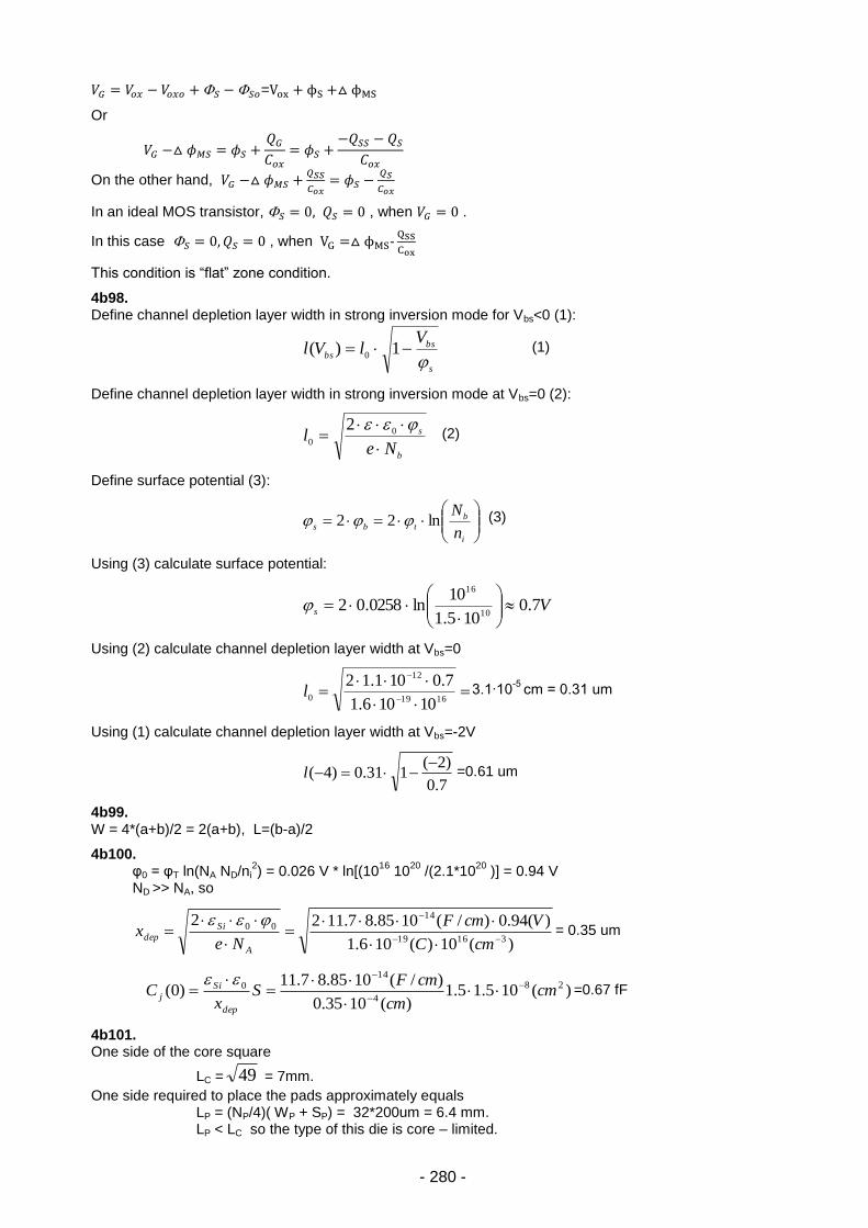
- 280 -
= ϕ ϕ
Or
On the other hand,
In an ideal MOS transistor, , when .
In this case , when ϕ -
This condition is “flat” zone condition.
4b98. Define channel depletion layer width in strong inversion mode for Vbs<0 (1):
s
bs
bs
VlVl
1)(
0 (1)
Define channel depletion layer width in strong inversion mode at Vbs=0 (2):
b
s
Nel
0
0
2 (2)
Define surface potential (3):
i
b
tbsn
Nln22 (3)
Using (3) calculate surface potential:
Vs
7.0105.1
10ln0258.02
10
16
Using (2) calculate channel depletion layer width at Vbs=0
1619
12
010106.1
7.0101.12l 3.1∙10
-5 cm = 0.31 um
Using (1) calculate channel depletion layer width at Vbs=-2V
7.0
)2(131.0)4(
l =0.61 um
4b99. W = 4*(a+b)/2 = 2(a+b), L=(b-a)/2
4b100. φ0 = φT ln(NA ND/ni
2) = 0.026 V * ln[(10
16 10
20 /(2.1*10
20 )] = 0.94 V
ND >> NA, so
)(10)(106.1
)(94.0)/(1085.87.112231619
14
00
cmC
VcmF
Nex
A
Si
dep
= 0.35 um
)(105.15.1)(1035.0
)/(1085.87.11)0( 28
4
14
0 cmcm
cmFS
xC
dep
Sij
=0.67 fF
4b101. One side of the core square
LC = 49 = 7mm.
One side required to place the pads approximately equals LP = (NP/4)( WP + SP) = 32*200um = 6.4 mm. LP < LC so the type of this die is core – limited.
- 281 -
5. SEMICONDUCTOR TECHNOLOGY
a) Test questions 5a1. E 5a2. D 5a3. D 5a4. D 5a5. B 5a6. C 5a7. B 5a8. B 5a9. B 5a10. A 5a11. B 5a12. B 5a13. C 5a14. A 5a15. B 5a16. D 5a17. C 5a18. D 5a19. C 5a20. C 5a21. B
5a22. C 5a23. B 5a24. C 5a25. B 5a26. A 5a27. E 5a28. D 5a30. C 5a31. A 5a32. A 5a33. C 5a34. A 5a35. B 5a36. D 5a37. B 5a38. C 5a39. A 5a40. A 5a41. E 5a42. C 5a43. C
5a44. A 5a45. A 5a46. A 5a47. C 5a48. E 5a49. B 5a50. C 5a51. B 5a52. C 5a53. B 5a54. D 5a55. D 5a56. B 5a57. B 5a58. B 5a59. B 5a60. E 5a61. E 5a62. E 5a63. C 5a64. B

- 282 -
b) Problems 5b1.
p=10-4
Ohm.m
n=10-2
Ohm.m
p=0,05 m2 V
-1 s
-1
n=0,13 m2 V
-1 s
-1
ni=1,38x10¹⁶
m-3
T=300K
c =
The contact potential is obtained from c= (kT/q )Inpp/pn=0,0258 Inpp/pn The densities of holes and electrons are obtained using the specific resistance expressions:
24
1941025,1
05,0106,110
11
q
m-3
21
192102,4
13,0106,110
11
nn
nq
n
m-3
The holes’ density in n region is obtained using the mass action law:
10
21
322
108,4102,4
102
n
in
n
n m
-3
The contact potential of p–n junction
c=0,0258 Inpp/pn=In1,25x1024
/4,8x1010
=0,8V. 5b2.
p=100 S/cm
p=1900 cm2 V
-1 s
-1
T=300 K ni =2,5x10
13 atom/cm
3
pp , np= Using the expression of the specific conductance
p=1/qppp, the holes’ density
17
191029,3
1900106,1
100
p
p
pq
p
cm
-3
The concentration of electrons is obtained using the mass action law: np pp= ni
2.
9
17
262
109,11029,3
1025,6
p
i
pp
nn cm
-3
5b3. Nd= 10
17atom/cm
3
L=100 μm W=10 μm d=1 μm
n= 1500 cm2 V
-1 s
-1
T=300K
R and s= Assuming that the impurities are fully ionized, the electrons concentration n =Nd The specific resistance
n =1/ =1/qnn, n=1/1,6x10-19
x1017
x1500= 0,042 Ohm cm The resistance
R=n L/ Wd =0,042 x10010-4
/10x10-4
x1x10-4
=4,2 kOhm. The sheet resistance
s=n/ d = 0,042/1x10-4
= 420 Ohm/mm. 5b4. C0x=100 nF/cm
2=100x10
-9 F/cm
2
ε SiO2=3,9x8,85x10-14
F/cm
tox= Calculate the thickness of SiO2 layer by the intrinsic formula of MOS-capacitor’s permittivity.
C0x= ε SiO2/ tox and tox= ε SiO2/ C0x
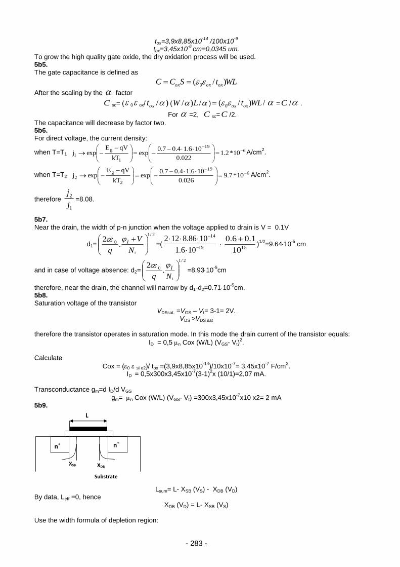
- 283 -
tox=3,9x8,85x10-14
/100x10-9
tox=3,45x10
-6 cm=0,0345 um.
To grow the high quality gate oxide, the dry oxidation process will be used. 5b5. The gate capacitance is defined as
WLtSCC oxoxox )/( 0
After the scaling by the factor
C sc= ( 0 ox/ )/oxt ( /)/ LW ) /)/( 0 WLtoxox = C / .
For =2, C sc= C /2.
The capacitance will decrease by factor two. 5b6. For direct voltage, the current density:
when T=T1 6
19
1
g
1 10*2.1022.0
106.14.07.0exp
kT
qVEexpj
A/cm
2.
when T=T2 6
19
2
g
2 10*7.9026.0
106.14.07.0exp
kT
qVEexpj
A/cm
2.
therefore
1
2
j
j=8.08.
5b7. Near the drain, the width of p-n junction when the voltage applied to drain is V = 0.1V
d1=
2/1
¹
0 .2
N
V
q
Ï
=(19
14
106.1
1086.8122
1510
1.06.0 )1/2
=9.6410-5
cm
and in case of voltage absence: d2=
2/1
¹
0 .2
Nq
Ï
=8.9310-5
cm
therefore, near the drain, the channel will narrow by d1-d2=0.7110-5
cm. 5b8. Saturation voltage of the transistor
VDSsat. =VGS – Vt= 3-1= 2V. VDS >VDS sat
therefore the transistor operates in saturation mode. In this mode the drain current of the transistor equals:
ID = 0,5 n Cox (W/L) (VGS- Vt)2.
Calculate
Cox = (0 si o2)/ tox =(3,9x8,85x10-14
)/10x10-7
= 3,45x10⁻⁷
F/cm2.
ID = 0,5x300x3,45x10-7
(3-1)2x (10/1)=2,07 mA.
Transconductance gm=d ID/d VGS
gm= n Cox (W/L) (VGS- Vt) =300x3,45x10-7
x10 x2= 2 mA 5b9.
Lsum= L- XSB (VS) - XDB (VD)
By data, Leff =0, hence XDB (VD) = L- XSB (VS)
Use the width formula of depletion region:
n+ n+
L
XSB XDB
Substrate
- 284 -
20 Si ( c - VD )/q Nsub = (L- XSB (0))2
VD=c - q Nsub(L- XSB (0))2/ 20 Si
Calculate
c =Tln Nsub Ndon/ ni2
In a room temperature
T ≈0,026 V and c ≈ 0,935 V.
XSB (0)=√ 20 Si c / q Nsub XSB (0)= √2x 8,85x10-14x11,8x0,935/1,6x10
-19x10
16
XSB (0) ≈0,349x10-4
cm. Put and calculate
lVDl ≈2,3 V. 5b10. Density of electronic current
Jn =eDn dN/dx According to Einstein formula:
Dn = T μn, and dN/dx =k
Jn =e T μn k
In a room temperature
T =0,026
V
Jn =1,6 10-19
x 0,026 x1200 x 8 x 1018
=39,936 A/cm2.
5b11.
a. Calculate the difference of contact potentials in E-B and C-B p-n junctions. At a room temperature
T ≈0,026 V
ce =Tln Ne Nb/ ni2
ce= 0,026 ln1019
x1015
/2,25x1020
≈0,8759 V
cc=Tln NbNc/ ni2
cc=0,026 ln1016
x5x1015
/2,25x1020
≈ 0,7 V b. Calculate E-B depletion layer width when the external voltage =0.
Xeb (0)=√ 20 Si ce / q Nb ≈3,38x10⁻⁵
cm=0,338 um. c. For base punch-through, Xcb depletion layer width must be
Xcb= 0,6 - 0,338= 0,262 um. d. The voltage of the collector can be obtained from the following equation:
Xcb = √ 20 Si Nc (cc-V) / q Nb (Nb+ Nc). Hence
V =cc - X2cb q Nb (Nb+ Nc) /20 Si Nc and |V| ≈0,8765 V
5b12. As Nd > Nacc, so silicon has an n – type conductivity. The active concentration of the impurities is Nact=
Ndon - Nacc = 9x10¹⁶
cm-3
. At room temperature T= 300 K all impurity atoms are ionized, Nact ≈ Ndon= n.
The specific conductivity of the sample at room temperature
n = e n n
n =1,6x10-19
C x 9x1016
cm-3
x 1400 cm2/Vs
n= 20,16 (Օhm cm)-1
.
5b13.
Тhe time delay in the n+
polysilicon interconnect line t=RC. The interconnect line resistance R= l/b:
R=200x1x103/1=200kOhm.
The interconnect line capacitance to the substrate C= CoS, C=60x103x1=60000 aF. Тhe time delay
t=200x103x60000x10
-18= 12 ns.
e b c
Wb
- 285 -
5b14. Тhe time delay in the metal interconnect line t=RC. The resistance of the metal 1 interconnect line
R= l/b R=0,1x1x10
3/0,2 =500 Ohm
The capacitance of the line to the substrate C= C0 S.
C=23 x 103 x 0,2=4600 aF.
Тhe time delay t= RC = 500x4600x10-18
= 2,3 ps.
5b15.
The p-n junction barrier layer capacitance C=(0Si/xp-n)Sp-n, where xp-n is the depletion width of the p-n
junction. For the one-sided p-n junction xp-n is defined as
xp-n≈xn= √20Si( k -U)/e Nd
xp-n=√ 2x 8,85x10-14
x11,8x(0,7-0)/1,6x10-19
x1016
=3x10⁻⁵
cm, when U=0V.
xp-n=√2x8,85x10-14
x11,8x(0,7+5)/1,6x10-19
x1016
=8,6x10⁻⁵
cm, when U= -5V.
The barrier layer capacitance
C0=(0Si/xp-n)Sp-n= (8,85x10-14
x11,8/3x10-5
) x10-5
=34,8x10⁻¹⁴
F=0,348 pF.
C5=(0Si/xp-n)Sp-n= (8,85x10-14
x11,8/ 8,6x10⁻⁵
) x10-5
=12,14x10⁻¹⁴
F=0,12 pF.
5b16. The time delay of the interconnect line
= RC
The resistance of the interconnect line R=sq (l/ w)
R=500(50/0,5)=50000 ohm.
The capacity of the interconnect line to the substrate
C=0ox(lw/tox)
C=8,8510-123,9 5010
-60,510
-6/0,210
-6=4,310
-15 F
= RC=500004,310-15
=0,21 ns.
5b17.
Power consumption P = IU
The current and voltage are scaled by factor. Thus,
Pscale = (I/)(U/)= P/2
The power density Pden = (IU)/(lw)= P/(lw)
Pscale =(P/2)/(I/w/)= P/(lw), so the power density does not change.
Time delay GRC
or GC
DDI/V , where G
C is the gate capacitance, and DD
I/V
is the effective
resistance of the gate capacitance.
For the scaled device
D
DG
I)
VC(
.
Time delay of the gate is reduced by factor.
The switching energy P
P
scale = (
32
P)
P
:
The switching energy is reduced by 3 times.
5b18. The temperature dependence of semiconductor resistor is expressed by
R= R0(1+(t-t0)).
So, R1= R0(1+(t1-t0)) and R2= R0(1+(t2-t0))
R = R2- R1 = R0(t2-t1)
- 286 -
Calculate the R0= sq (l/ w)= 300(510-5
/2,510-6
)=6000 ohm.
R =6000 0,0024100 =1440 ohm. 5b19.
The resistance of emitter n+ region is R=sq(l/ b):
sq =/h, and =1/σ, we obtain sq =1/ σh . Calculate the σ specific conductivity
σ = e n n and n = Ndon
σ =1,610-1910
250,14= 2,2410
5 1/ohmm
sq=1/ σh= 1/2,2410510
-7 = 44,6 ohmm:
R=sq (l/ b)= 44,6(10-5
/510-7
)= 892 ohm. 5b20. The diffusion current density of electrons equals: Jn= eDndn/dx ≈ eDn Δn/Δx. At room temperature n ≈ Nd. The diffusion coefficient Dn is obtained from the Einstein relation:
Dn=(kT/e)μn= t μn
Dn= 0,026·1200= 31,2 cm2/s
The concentration gradient Δn/Δx =(1018
- 5·1017
)/3·10-4
≈ 1,66 ·1021
cm-4
. Jn=1,6·10
-19·31,2· 1,66 ·10
21 = 8,286 ·10
3 A/cm
2
5b21. The resolution R and focus depth F of the optical system are expressed by:
R=K1/NA and F=K2/(NA)2 respectively.
R=0,3x193/0,65 =89 nm, F=0,5x193/(0,65)2 =228,4 nm.
To improve the resolution of the optical system, immersion lithography technology is used. Immersion lithography is an optical technique of improvement that increases the effective aperture NA of the optical system. The aperture NA=n x sinα, where n is a refractive index of a fluid (such as water) between the final lens and the wafer surface. The resolution is increased by a factor equal to the refractive index of the liquid. It is possible to increase resolution while simultaneously maintaining practical depths of focus. Current immersion lithography tools use highly purified water for this liquid, achieving feature sizes below 45 nanometers. 5b22. As (VGS - Vt )= VDS sat < VDS, there are saturation mode and MOS transistor current:
2))(/(5,0 tGSoxDS VVLWCI
Calculate Cox=εoεox/tox Cox=8,85x10
-12x3,9/15x10
-9 =2,3x10
-3 F/m
2
IDS=0,5x 500 x10-4
x2,3x10-3
(5/0,3) (1,5- 0,7)2=613,3 mkA.
Тhе differential resistance R of a MOS transistor may be obtained as: R=dV/dI= 1/dI/dV,
R=1/ ))(/( tGSox VVLWC
R=1/500 x10-4
x2,3x10-3
(5/0,3)(1,5-0,7)=652 Ohm. 5b23. The temperature dependence of a semiconductor resistor is expressed by:
R= R0(1+(t-t0)).
At room temperature t1= t0 , and R1= R0(1+(t1-t0)) = R0 .
R2= R0(1+(t2-t0)) at t2 temperature. R2= R1 + 0,5 R1 = 1,5 R1.
So, R0(1+(t2-t0))= R0 , and t2 = 0,5/ + t0 =178,5oC.
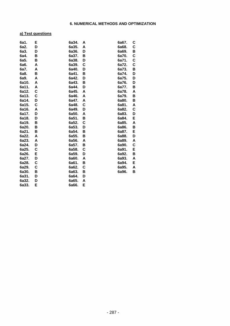
- 287 -
6. NUMERICAL METHODS AND OPTIMIZATION
a) Test questions 6a1. E 6a2. D 6a3. D 6a4. B 6a5. B 6a6. A 6a7. A 6a8. B 6a9. A 6a10. A 6a11. A 6a12. C 6a13. C 6a14. D 6a15. C 6a16. A 6a17. D 6a18. D 6a19. B 6a20. B 6a21. B 6a22. A 6a23. A 6a24. D 6a25. C 6a26. E 6a27. D 6a28. C 6a29. C 6a30. B 6a31. D 6a32. D 6a33. E
6a34. A 6a35. A 6a36. D 6a37. B 6a38. D 6a39. C 6a40. D 6a41. B 6a42. D 6a43. B 6a44. D 6a45. A 6a46. A 6a47. A 6a48. C 6a49. D 6a50. A 6a51. B 6a52. C 6a53. D 6a54. B 6a55. B 6a56. A 6a57. B 6a58. C 6a59. D 6a60. A 6a61. B 6a62. C 6a63. B 6a64. D 6a65. A 6a66. E
6a67. C 6a68. C 6a69. B 6a70. C 6a71. C 6a72. C 6a73. B 6a74. D 6a75. D 6a76. D 6a77. B 6a78. A 6a79. B 6a80. B 6a81. A 6a82. C 6a83. D 6a84. E 6a85. A 6a86. B 6a87. E 6a88. D 6a89. A 6a90. C 6a91. E 6a92. B 6a93. A 6a94. E 6a95. A 6a96. B
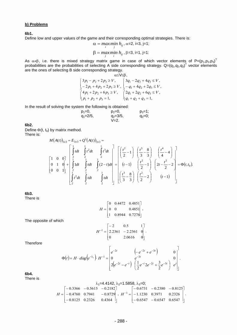
- 288 -
b) Problems 6b1. Define low and upper values of the game and their corresponding optimal strategies. There is:
ijji
hminmax , =2, i=3, j=1;
ijij
hminmax , =3, i=1, j=1:
As , i.e. there is mixed strategy matrix game in case of which vector elements of P=(p1,p2,p3)T
probabilities are the probabilities of selecting A side corresponding strategy. Q=(q1,q2,q3)T vector elements
are the ones of selecting B side corresponding strategy.
V,
,ppp
,Vppp
,Vppp
,Vppp
1
624
242
23
321
321
321
321
,qqq
,Vqqq
,Vqqq
,Vqqq
1
622
24
423
321
321
321
321
In the result of solving the system the following is obtained: p1=0, p2=0, p3=1; q1=2/5, q2=3/5, q3=0;
V=2. 6b2.
Define (t, t0) by matrix method. There is:
.,
1223
8
3
22
212
1
443
8
31
2
)2(1
100
010
001
)()(
0
23
22
432
1
2
1
2
1
2
2
1
2
1
2
1
2
1
2
3
1
2
2
1
2
331
3333
tt
ttt
tt
tt
ttt
tdttdtdtt
dtttdtdt
dttdtttdt
tAQEtAM xxx
6b3. There is
72760894401
4851000
48510447200
..
.
..
H ,
The opposite of which
0061620
02361223612
15021
.
..
.
H .
Therefore
tttttt
t
ttt
eeeeee
e
eee
HediagHt i
322
3
322
1
2
32
2
12
00
0λ
.
6b4. There is
1=4.4142, 2=1.5858, 3=0;
436402326081250
872907941047600
218205615033660
...
...
...
H ,
654706547065470
232603971012301
8125023800673101
...
...
...
H .
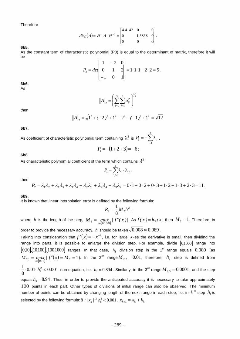
- 289 -
Therefore
000
0585810
00414241 .
.
HAHAdiag .
6b5. As the constant term of characteristic polynomial (P3) is equal to the determinant of matrix, therefore it will be
522111
101
210
021
3
detP .
6b6. As
21
3
1
3
1
2
2
i j
ijaA
then
12112121 222222
2 )()(A
6b7.
As coefficient of characteristic polynomial term containing 2 is
3
1
1
i
iP ,
63211 P :
6b8.
As characteristic polynomial coefficient of the term which contains 2
4
1
1
j,i
jiP ,
then
113231213020104342324131212 P .
6b9. It is known that linear interpolation error is defined by the following formula:
2
228
1hMR ,
where h is the length of the step,
|)x(f|maxM,x
10000
2. As xlog)x(f , then 12 M . Therefore, in
order to provide the necessary accuracy, h should be taken 0.089008.0 .
Taking into consideration that 2 xxf , i.e. for large x -es the derivative is small, then dividing the
range into parts, it is possible to enlarge the division step. For example, divide 10000, range into
100010010010100 ,,,,, ranges. In that case, 1h division step in the 1st range equals 0890. (as
12
10012
M|xf|maxM
,x,
). In the 2nd
range 01022 .M , , therefore, 2h step is defined from
00100108
1 2
2 .h. non-equation, i.e. 0.8942 h . Similarly, in the 3rd
range 0001032 .M , , and the step
equals 9483 .h . Thus, in order to provide the anticipated accuracy it is necessary to take approximately
100 points in each part. Other types of divisions of initial range can also be observed. The minimum
number of points can be obtained by changing length of the next range in each step, i.e. in k th step kh is
selected by the following formula: 00108 221 .h|x| kk , kkk hxx 1 .
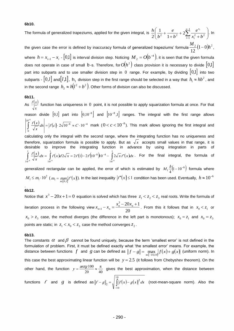
- 290 -
6b10.
The formula of generalized trapeziums, applied for the given integral, is
1
12222
21
1
2
n
i i
x
bx
e
b
e
b
h i
. In
the given case the error is defined by inaccuracy formula of generalized trapeziums’ formula 22 0112
hM
,
where ii xxh 1 - 10, is interval division step. Noticing 4
2
bOM , it is seen that the given formula
does not operate in case of small b -s. Therefore, for 2hO class provision it is necessary to divide 10,
part into subparts and to use smaller division step in 0 range. For example, by dividing 1,0 into two
subparts - l,0 and 1,l , 1h division step in the first range should be selected in a way that 2
1 hbh , and
in the second range 22
2 blhh . Other forms of division can also be discussed.
6b11.
As x
xf function has uniqueness in 0 point, it is not possible to apply squarization formula at once. For that
reason divide 10, part into 8100 , and 110 8 , ranges. The integral with the first range allows
48
10
0
10102
8
Ccfdxx
xf mark (
8100 c ). This mark allows ignoring the first integral and
calculating only the integral with the second range, where the integrating function has no uniqueness and
therefore, squarization formula is possible to apply. But as x accepts small values in that range, it is
desirable to improve the integrating function in advance by using integration in parts of
1
10
48
1
10
1
10 888
210102122 dxxfxffxdxfdxx
xf. For the final integral, the formula of
generalized rectangular can be applied, the error of which is estimated by 81 101
4
h
M formula where
211 10 mM (
xfmaxm
,x
101 ). In the last inequality 1 xf condition has been used. Eventually,
610h
. 6b12.
Notice that 01203 xx equation is solved which has three 321 zzz real roots. Write the formula of
iteration process in the following view20
1203
1
nnnn
xxxx . From this it follows that in 10 zx or
30 zx case, the method diverges (the difference in the left part is monotonous); 10 zx and 30 zx
points are static; in 301 zxz case the method converges 2z .
6b13.
The constants and cannot be found uniquely, because the term ‘smallest error’ is not defined in the
formulation of problem. First, it must be defined exactly what ‘the smallest error’ means. For example, the
distance between functions f and g can be defined as
xgxfgfx
10,10
max (uniform norm). In
this case the best approximating linear function will be 5.2y (it follows from Chebyshev theorem). On the
other hand, the function 4020
100 π
arctgy gives the best approximation, when the distance between
functions f and g is defined as
10
10
2
2dxxgxfgf (root-mean-square norm). Also the
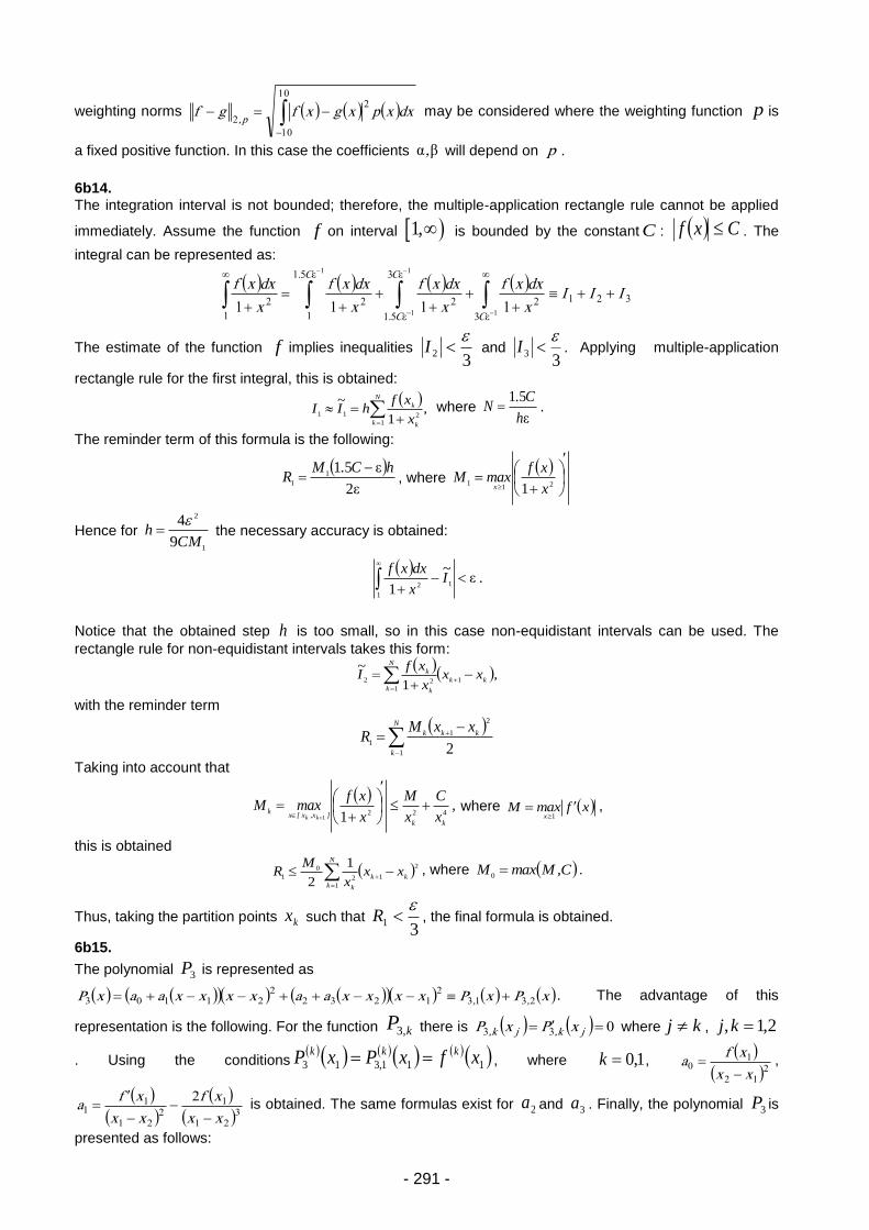
- 291 -
weighting norms
10
10
2
2dxxpxgxfgf
p, may be considered where the weighting function p is
a fixed positive function. In this case the coefficients βα, will depend on p .
6b14. The integration interval is not bounded; therefore, the multiple-application rectangle rule cannot be applied
immediately. Assume the function f on interval 1, is bounded by the constant C : Cxf . The
integral can be represented as:
1
1
1
1
3
3212
3
51
2
51
1
2
1
2 1111ε
ε
ε
ε
C
C
C.
C.
IIIx
dxxf
x
dxxf
x
dxxf
x
dxxf
The estimate of the function f implies inequalities 3
2
I and
33
I . Applying multiple-application
rectangle rule for the first integral, this is obtained:
,
x
xfhI
~I
N
k k
k
1
2111
where ε
51
h
C.N .
The reminder term of this formula is the following:
ε2
ε511
1
hC.MR
, where
211
1 x
xfmaxM
x
Hence for 1
2
9
4
CMh
the necessary accuracy is obtained:
ε
11
12
I~
x
dxxf.
Notice that the obtained step h is too small, so in this case non-equidistant intervals can be used. The
rectangle rule for non-equidistant intervals takes this form:
,xxx
xfI~
kk
N
k k
k
1
122
1
with the reminder term
N
k
kkkxxM
R1
2
1
12
Taking into account that
,
x
C
x
M
x
xfmaxM
kk]x,x[x
kkk
42211
where xfmaxM
x
1,
this is obtained
2
1
12
0
1
1
2kk
N
k k
xxx
MR
, where C,MmaxM 0
.
Thus, taking the partition points kx such that 3
1
R , the final formula is obtained.
6b15.
The polynomial 3P is represented as
xPxPxxxxaaxxxxaaxP ,, 23132
12322
21103 . The advantage of this
representation is the following. For the function kP ,3 there is 033 jk,jk, xPxP where kj , 2,1, kj
. Using the conditions 111,313 xfxPxP kkk , where 1,0k ,
212
10
xx
xfa
,
321
1
221
11
2
xx
xf
xx
xfa
is obtained. The same formulas exist for 2a and 3a . Finally, the polynomial 3P is
presented as follows:
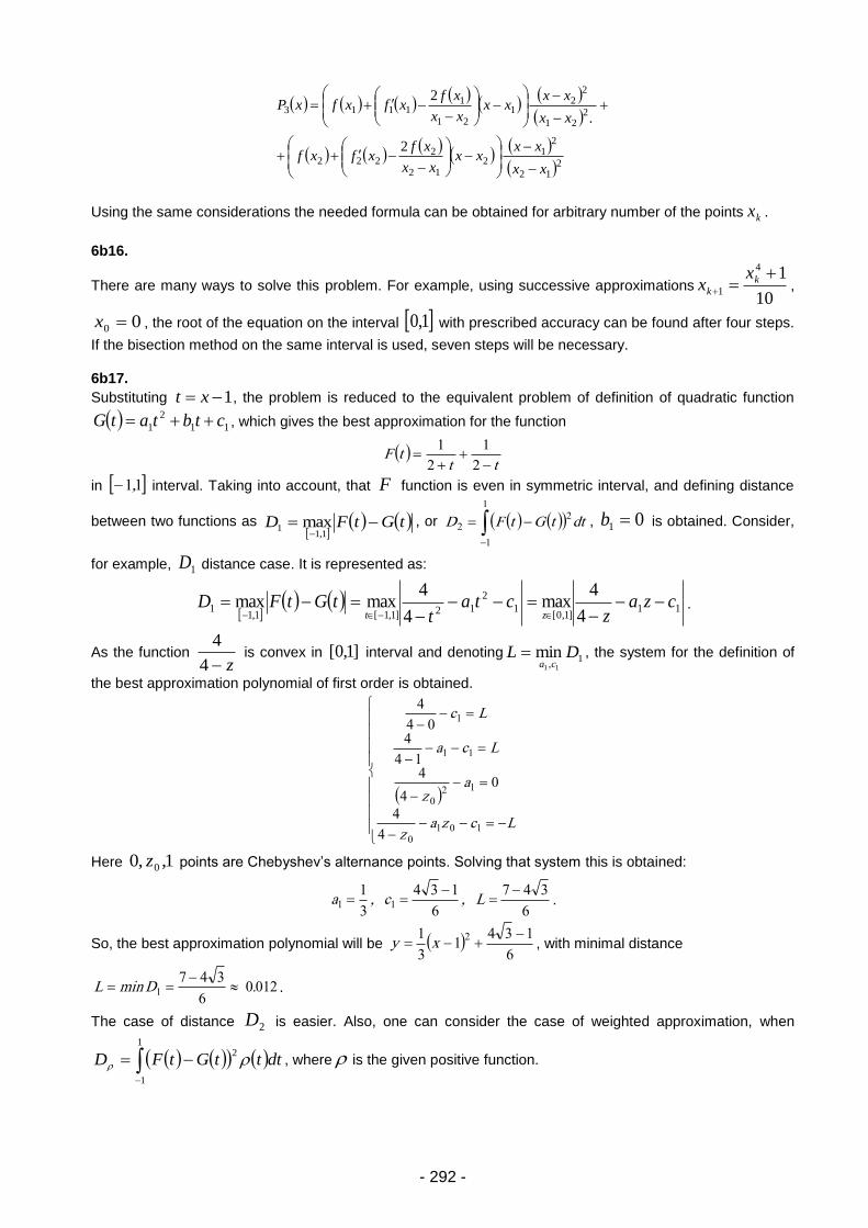
- 292 -
212
21
212
2222
221
22
121
11113
2
.
2
xx
xxxx
xx
xfxfxf
xx
xxxx
xx
xfxfxfxP
Using the same considerations the needed formula can be obtained for arbitrary number of the points kx .
6b16.
There are many ways to solve this problem. For example, using successive approximations10
14
1
kk
xx ,
00 x , the root of the equation on the interval 1,0 with prescribed accuracy can be found after four steps.
If the bisection method on the same interval is used, seven steps will be necessary. 6b17.
Substituting 1 xt , the problem is reduced to the equivalent problem of definition of quadratic function
11
2
1 ctbtatG , which gives the best approximation for the function
tt
tF
2
1
2
1
in 11, interval. Taking into account, that F function is even in symmetric interval, and defining distance
between two functions as
tGtFD 1,1
1 max , or
1
1
22 dttGtFD , 01 b is obtained. Consider,
for example, 1D distance case. It is represented as:
11
]1,0[1
2
12]1,1[1,11
4
4max
4
4maxmax cza
zcta
ttGtFD
zt
.
As the function z4
4 is convex in ]1,0[ interval and denoting
1, 11
min DLca
, the system for the definition of
the best approximation polynomial of first order is obtained.
Lczaz
az
Lca
Lc
1010
120
11
1
4
4
04
414
404
4
Here 1,,0 0z points are Chebyshev’s alternance points. Solving that system this is obtained:
6
347
6
134
3
111
L,c,a .
So, the best approximation polynomial will be 6
1341
3
1 2 xy , with minimal distance
01206
3471 .DminL
.
The case of distance 2D is easier. Also, one can consider the case of weighted approximation, when
1
1
2dtttGtFD , where is the given positive function.
- 293 -
6b18.
Calculating n , 11 2 nnn recurrent formula for 1n is obtained. Solving it, nCCn 21 is
obtained, where 1C and 2C are unknown constants. As 21 and 32 , 1 nn . So, 1lim
n
n
n
is obtained. 6b19.
One of possible ways. Assume the equation of AB line is 0, cbyaxyxl . This line splits the
plane into two half-planes: 0,:, yxlyx and 0,:, yxlyx . If the point D lies in triangle’s
interior, then substituting the coordinates of that and C point into yxl , , values of the same sign will be
obtained (i.e. D and C belong to the same half-plane). The same considerations can be done for BC
and AC lines. An arbitrary polygon case can be reduced to triangle case by partitioning and checking if D
point lies in one of partition triangles. 6b20.
The polynomial 4P is represented as:
0
4
1
3
13
2
1211024 bxxxxaxxaxxaaxxP .
Substituting that polynomial into the given equalities, the system for determination of unknown ka and 0b is
obtained:
40
4
12 ybxx ,
33212
22211
11210
0021
66
22
yaxxa
yaxxa
yaxxa
yaxx
.
The general case may be considered analogously. 6b21. As characteristic polynomial’s absolute term (P3) equals to determinant of matrix, then it will be
723111
101
210
031
3
detP .
6b22. As
17112131 222222
21
3
1
3
1
2
2
)()(aAi j
ij.
6b23.
As the coefficient of first degree of in the characteristic polynomial
3
1
1
i
iP , then :P 72411
6b24.
A As the coefficient of first degree of 2 in the characteristic polynomial
4
1
1
j,i
jiP , then
353231213424144342324131212 P
6b25.
There are five linearly independent conditions for determination of the nP polynomial coefficients. Therefore,
the minimal value of n for which the problem has a solution for arbitrary values jy and kz cannot be less
- 294 -
than four. Forth order polynomial which satisfies given conditions, can be found explicitly, similar to Lagrange
interpolation polynomial. First, find basic polynomials j and k , satisfying conditions:
2,1,0,1 iij
i
j , 1,0,00 qq
j , for 2,1,0j
2,1,0,01 ii
k , 1,0,0 qkq
q
k for 1,0k .
Here ij is a Kronecker symbol ( 0ij for ji and 1ii ). After that, the required polynomial is found
by the formula
xzxzxyxPj
jj 1100
2
0
4
.
Show how to construct basic polynomials. Consider, for example, 1 .
Search this polynomial in the form
bxaxxx 112
1 .
Then the constants ba, will be determined from the conditions 01,11 11 , or
042,1 bab , from which 1,2 ba . The remaining basic polynomials can be found
analogously.
The polynomials 4P can be found also directly, by writing it down as:
edxxcxbxaxxP 322
4 111 , and determining coefficients edcba ,,,, from
problem conditions by constants jy and kz .
6b26.
As the function 3xxf is odd, and an interval 1,1 is symmetric relative to origin, then the required
polynomial has to be an odd function, too. Hence, axxP 1 , where the constant a must be determined.
For the determination of this constant, consider the function axxxPxfxg 3
1 on the interval
1,0 . There is 00 g and ag 11 . The function g is convex, therefore a can be found from the
condition, that the minimal value of function g at some point 0x of open interval 1,0 is equal to
ag 11 with opposite sign. Then in the interval 1,1 four points ( 1,,,1 403021 zxzxzz )
are obtained, where 11 1 PfzPzfk
kk , so, by the Chebyshev theorem, the polynomial axP 1
will be the required polynomial of best approximation. So:
axxg 23 , from which 3
0
ax . Further,
33
2
3
aa
ag
, and therefore the constant a can be found
from equation 33
21
aaa . Solving this equation,
4
3a is obtained. Finally, the polynomial of best
approximation is xxP4
31 . This problem can be solved easier, using geometric considerations.
6b27.
Assume is eigenvalue of A matrix. In that case 0det EA ( E is unit matrix). If A matrix satisfies
0nA condition, where n is a natural number, then there is
EAAAEAEAE nnnnnnn 13221 ,
therefore, using the properties of determinants
0detdetdet 132211 EAAAEAE nnnnnn
i.e. 0 . Thus if 0nA , where n is a natural number, the eigenvalue of A matrix equals zero.
- 295 -
6b28.
Substituting 1 in the expansion of the logarithm function alternating series
1
1 112ln
k
k
k is obtained
which converges very slowly as, according to Leibniz theorem, 1
12ln
NSN , where
NS is a partial
sum of the given series. Therefore, to provide the necessary accuracy it is necessary to take not less than 1000 terms of the series which leads to significant increase of round-off error. Therefore it is better to apply
the following method. Define t number from equation 21
1
t
t .
3
1t is obtained hence, the seeking
number is presented as:
0
1
3
111
3
11
3
112
kk
k
klnlnln
This series in the right part may be estimated by geometrical progression with 3
1 denominator. Therefore in
order to provide the necessary accuracy it is enough to take only 8 summands of the given series. The same method may be applied again. Other methods are also possible.
6b29. As the absolute term (P3) of characteristic polynomial equals to determinant of matrix, then it will be
:)()(detP 56426222
202
420
062
3
6b30.
As the coefficient of 2 in the characteristic polynomial is equal to
4
ji1j,i
ji2P , then
:75.85.175.05.03215.115.15.015.05.12125.02
P 4342324131212
6b31. As the characteristic equation looks as follows,
,)()(AE 0232111
02 2
λλλλ
λ
λλ
the eigenvalues .1,2 21 The eigenvector, which corresponds to 1 , has to be found from the
homogeneous linear system T
21111 )h,h(h :
,h
h
h
h
21
11
21
112
11
02
and in the same way, the eigenvector T
22122 )h,h(h , which corresponds to 2 , may be found from
,h
h
h
h
22
12
22
121
11
02
hence ,0h12 and for 22h , 1h 22 can be chosen.
Solving these systems, the following is obtained:
1
0
1
1
22
12
21
11
h
h
h
h
So transform matrix is
11
01H
for which HH 1 .
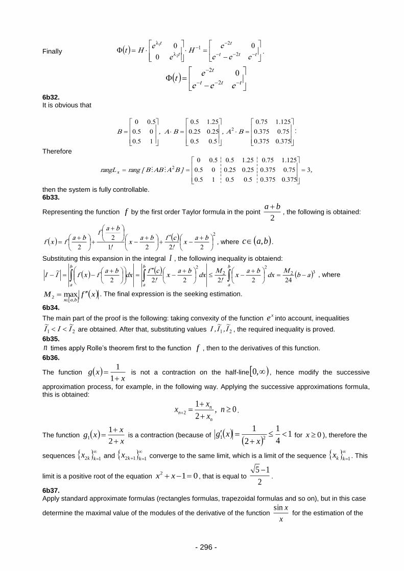
- 296 -
Finally
ttt
t
t
t
eee
eH
e
eHt
2
21 0
0
0
2
1
λ
λ
.
6b32. It is obvious that
37503750
7503750
1251750
5050
250250
25150
150
050
5002
..
..
..
BA,
..
..
..
BA,
.
.
.
B :
Therefore
,
.....
.....
.....
]BAABB[rangrangLx 3
375037505050150
7503750250250050
1251750251505002
then the system is fully controllable. 6b33.
Representing the function f by the first order Taylor formula in the point 2
ba , the following is obtained:
2
2221
2
2
bax
!
cfbax
!
baf
bafxf , where bac , .
Substituting this expansion in the integral I , the following inequality is obtaiend:
32
2
2
2
2422222ab
Mdx
bax
!
Mdx
bax
!
cfdx
bafxfI
~I
b
a
b
a
b
a
, where
xfM
bax
,2 max . The final expression is the seeking estimation.
6b34.
The main part of the proof is the following: taking convexity of the function xe into account, inequalities
21 I~
II~
are obtained. After that, substituting values 21 I~
,I~
,I , the required inequality is proved.
6b35.
n times apply Rolle’s theorem first to the function f , then to the derivatives of this function.
6b36.
The function x
xg
1
1 is not a contraction on the half-line ,0 , hence modify the successive
approximation process, for example, in the following way. Applying the successive approximations formula, this is obtained:
0,2
12
n
x
xx
n
nn .
The function x
xxg
2
11 is a contraction (because of
1
4
1
2
121
xxg for 0x ), therefore the
sequences 12 kkx and
112 kkx converge to the same limit, which is a limit of the sequence 1kkx . This
limit is a positive root of the equation 012 xx , that is equal to 2
15 .
6b37. Apply standard approximate formulas (rectangles formulas, trapezoidal formulas and so on), but in this case
determine the maximal value of the modules of the derivative of the function x
xsin for the estimation of the
ttt
t
eee
et
2
2 0
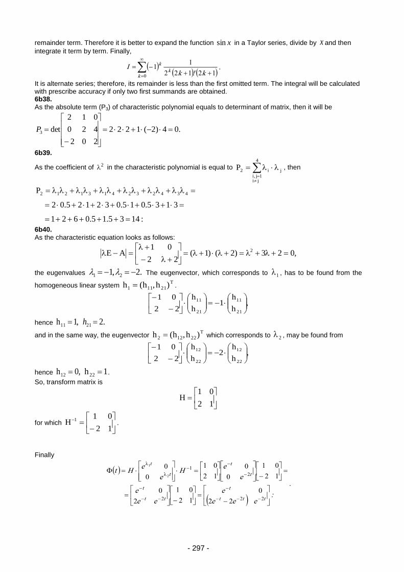
- 297 -
remainder term. Therefore it is better to expand the function xsin in a Taylor series, divide by x and then
integrate it term by term. Finally,
0 12122
11
kk
k
k!kI .
It is alternate series; therefore, its remainder is less than the first omitted term. The integral will be calculated with prescribe accuracy if only two first summands are obtained. 6b38. As the absolute term (P3) of characteristic polynomial equals to determinant of matrix, then it will be
.04)2(1222
202
420
012
det3
P
6b39.
As the coefficient of 2 in the characteristic polynomial is equal to
4
ji1j,i
ji2P , then
:1435.15.0621
3135.015.032125.02
P 4342324131212
6b40. As the characteristic equation looks as follows:
,023)2()1(22
01AE 2
the eugenvalues .2,1 21 The eugenvector, which corresponds to 1 , has to be found from the
homogeneous linear system T
21111 )h,h(h .
,h
h1
h
h
22
01
21
11
21
11
hence ,1h11 .221 h
and in the same way, the eugenvector T
22122 )h,h(h which corresponds to 2 , may be found from
,h
h2
h
h
22
01
22
12
22
12
hence ,0h12 1h 22 .
So, transform matrix is
12
01H
for which
12
01H 1
.
Finally
:
eee
e
ee
e
e
eH
e
eHt
ttt
t
tt
t
t
t
t
t
222
2
1
22
0
12
01
2
0
12
01
0
0
12
01
0
0
2
1
λ
λ
.
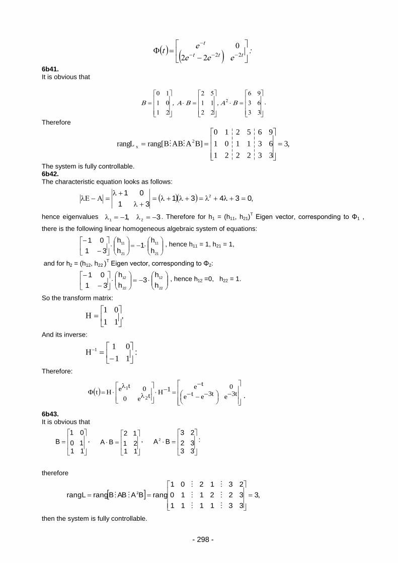
- 298 -
:eee
et
ttt
t
2222
0
6b41. It is obvious that
33
63
96
22
11
52
21
01
102 BA,BA,B .
Therefore
,3
332221
631101
965210
]BAABB[rangrangL 2
x
The system is fully controllable. 6b42. The characteristic equation looks as follows:
,0343131
012
hence eigenvalues ,11
32
. Therefore for h1 = (h11, h21)T Eigen vector, corresponding to Φ1 ,
there is the following linear homogeneous algebraic system of equations:
21
11
21
11
h
h1
h
h
31
01 , hence h11 = 1, h21 = 1,
and for հ2 = (h12, h22 )T Eigen vector, corresponding to Φ2:
22
12
22
12
h
h3
h
h
31
01 , hence հ12 =0, h22 = 1.
So the transform matrix:
,
11
01
And its inverse:
:
11
011
Therefore:
t3et3ete
0te1t
e0
0t
et
2
1
.
6b43. It is obvious that
111
0
0
1
B ,
112
1
1
2
BA ,
333
2
2
3
BA 2 :
therefore
,3
331111
322110
231201
rangBAABBrangrangL 2
then the system is fully controllable.
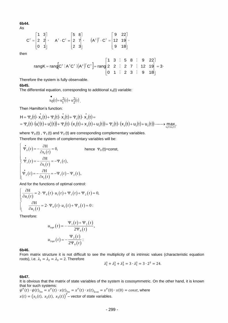
- 299 -
6b44. As
10
22
31
CT ,
32
72
85
CA TT ,
189
1912
229
CA TT2 ,
then
3
1893210
19127222
2298531
rangCACACrangrangK TT2TTT
.
Therefore the system is fully observable.
6b45. The differential equation, corresponding to additional x0(t) variable:
t22
ut21
ut0x
.
Then Hamilton’s function:
,maxtututxttutxtxttutut
txttxttxtH
tu,tu21221211
2
2
2
10
221100
21
where 0 (t) , 1 (t) and 2 (t) are corresponding complementary variables.
Therefore the system of complementary variables will be:
0
0
1 1
1
2 1 2
2
0,
,
,
tx t
t tx t
t t tx t
And for the functions of optimal control:
0 1 1 2
1
0 2 2
2
2 0,
2 0 :
t u t t tu t
t u t tu t
Therefore:
1 2
1
0
2
2
0
,2
:2
opt
opt
t tu t
t
tu t
t
6b46. From matrix structure it is not difficult to see the multiplicity of its intrinsic values (characteristic equation roots), i.e. Therefore
6b47. It is obvious that the matrix of state variables of the system is cososymmetric. On the other hand, it is known that for such systems:
( ) ( ) ( ) ( )
( ) ( ) ( ) ( ) 𝑜 where
( ) ( ( ) ( ) ( )) – vector of state variables.
hence 0 (t)=const,
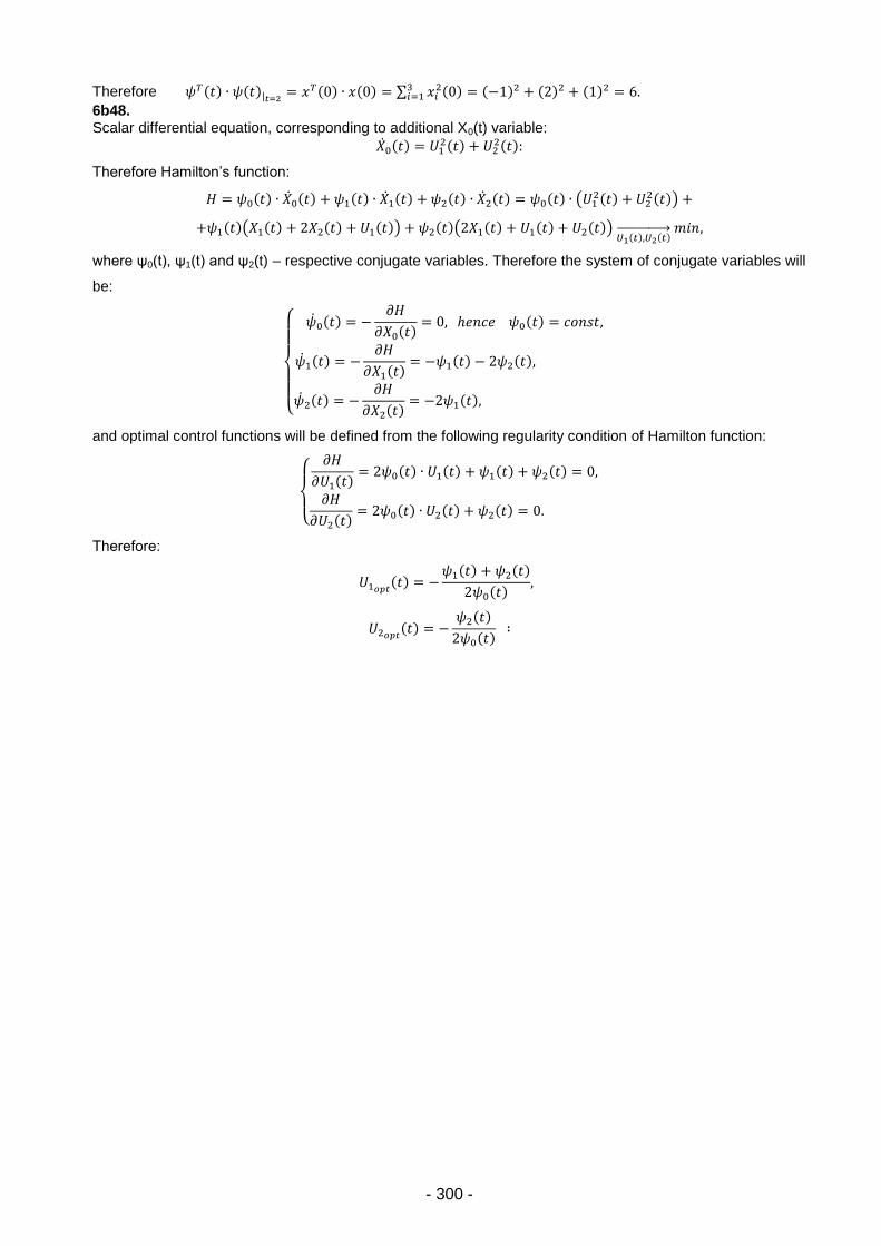
- 300 -
Therefore ( ) ( ) ( ) ( ) ∑
( ) ( ) ( ) ( )
6b48. Scalar differential equation, corresponding to additional X0(t) variable:
( ) ( )
( )
Therefore Hamilton’s function:
( ) ( ) ( ) ( ) ( ) ( ) ( ) ( ( )
( ))
( )( ( ) ( ) ( )) ( )( ( ) ( ) ( )) ( ) ( )→
where ψ0(t), ψ1(t) and ψ2(t) – respective conjugate variables. Therefore the system of conjugate variables will
be:
{
( )
( ) ( ) 𝑜
( )
( ) ( ) ( )
( )
( ) ( )
and optimal control functions will be defined from the following regularity condition of Hamilton function:
{
( ) ( ) ( ) ( ) ( )
( ) ( ) ( ) ( )
Therefore:
( ) ( ) ( )
( )
( ) ( )
( )
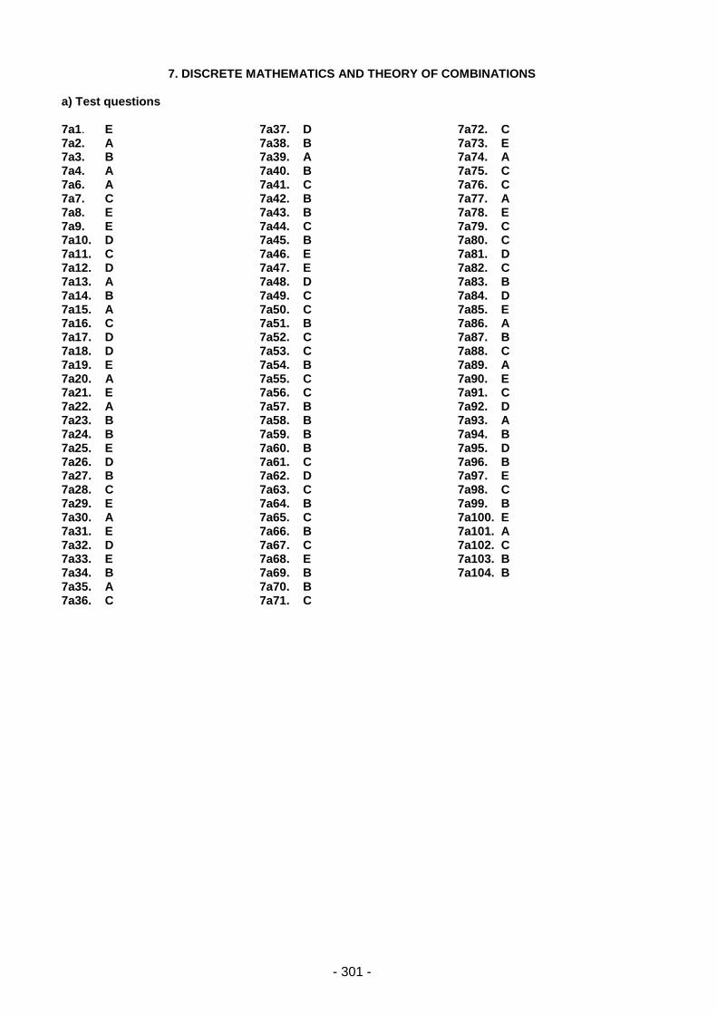
- 301 -
7. DISCRETE MATHEMATICS AND THEORY OF COMBINATIONS a) Test questions 7a1. E 7a2. A 7a3. B 7a4. A 7a6. A 7a7. C 7a8. E 7a9. E 7a10. D 7a11. C 7a12. D 7a13. A 7a14. B 7a15. A 7a16. C 7a17. D 7a18. D 7a19. E 7a20. A 7a21. E 7a22. A 7a23. B 7a24. B 7a25. E 7a26. D 7a27. B 7a28. C 7a29. E 7a30. A 7a31. E 7a32. D 7a33. E 7a34. B 7a35. A 7a36. C
7a37. D 7a38. B 7a39. A 7a40. B 7a41. C 7a42. B 7a43. B 7a44. C 7a45. B 7a46. E 7a47. E 7a48. D 7a49. C 7a50. C 7a51. B 7a52. C 7a53. C 7a54. B 7a55. C 7a56. C 7a57. B 7a58. B 7a59. B 7a60. B 7a61. C 7a62. D 7a63. C 7a64. B 7a65. C 7a66. B 7a67. C 7a68. E 7a69. B 7a70. B 7a71. C
7a72. C 7a73. E 7a74. A 7a75. C 7a76. C 7a77. A 7a78. E 7a79. C 7a80. C 7a81. D 7a82. C 7a83. B 7a84. D 7a85. E 7a86. A 7a87. B 7a88. C 7a89. A 7a90. E 7a91. C 7a92. D 7a93. A 7a94. B 7a95. D 7a96. B 7a97. E 7a98. C 7a99. B 7a100. E 7a101. A 7a102. C 7a103. B 7a104. B
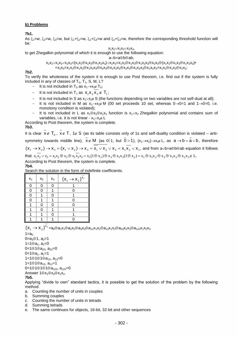
- 302 -
b) Problems 7b1.
As 1=w, 2=w, 3=w, but 1+2=w, 1+3=w and 2+3=w, therefore the corresponding threshold function will be:
x1x2x1x3x2x3, to get Zhegalkin polynomial of which it is enough to use the following equation:
ab=abab,
x1x2x1x3x2x3=(x1x2x1x3x1x2x3)x2x3=x1x2x1x3x1x2x3x2x3(x1x2x1x3x1x2x3)
x2x3=x1x2x1x3x1x2x3x2x3x1x2x3x2x3x1x2x3x1x2x3=x1x2x1x3x2x3: 7b2. To verify the wholeness of the system it is enough to use Post theorem, i.e. find out if the system is fully included in any of classes of T0, T1, S, M, L?
- It is not included in T0 as x1x2T0;
- It is not included in T1 as 1321 Txxx ;
- It is not included in S as x1x2S (the functions depending on two variables are not self-dual at all);
- It is not included in M as x1x2M (00 set proceeds 10 set, whereas 00=1 and 10=0, i.e. monotony condition is violated);
- It is not included in L as x1x2x1x2 function is x1x2 Zhegalkin polynomial and contains sum of
variables, i.e. it is not linear - x1x2L According to Post theorem, the system is complete. 7b3.
It is clear 0Tx , Tx , S1 (as its table consists only of 1s and self-duality condition is violated – anti-
symmetry towards middle line), Mx (as 01, but 10 ), (x1x2)x3L, as baba , therefore
321321321321 xxxxxxx)xx(x)xx( , and from ab=abab equation it follows
that L.xxxxxxxx)x(1xxx)x(1x 32313211231321321321321 xxxxxxxxx
According to Post theorem, the system is complete. 7b4. Search the solution in the form of indefinite coefficients.
x1 x2 x3 3
21
x)xx(
0 0 0 1
0 0 1 0
0 1 0 1
0 1 1 0
1 0 0 0
1 0 1 1
1 1 0 1
1 1 1 0
3
21
x)xx( =a0a1x1a2x2a3x3a12x1x2a13x1x3a23x2x3a123x1x2x3
1=a0
0=a31, a3=1
1=1a2, a2=0
0=11a23, a23=0
0=1a1, a1=1
1=111a13, a13=0
1=11a12, a12=1
0=1111a123, a123=0
Answer 1x1x3x1x2. 7b5. Applying “divide to own” standard tactics, it is possible to get the solution of the problem by the following method: a. Counting the number of units in couples b. Summing couples c. Counting the number of units in tetrads d. Summing tetrads e. The same continues for objects, 16-bit, 32-bit and other sequences
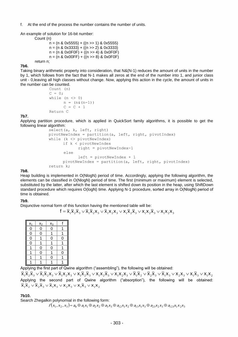
- 303 -
f. At the end of the process the number contains the number of units. An example of solution for 16-bit number:
Count (n) n = (n & 0x5555) + ((n >> 1) & 0x5555) n = (n & 0x3333) + ((n >> 2) & 0x3333) n = (n & 0x0F0F) + ((n >> 4) & 0x0F0F) n = (n & 0x00FF) + ((n >> 8) & 0x0F0F)
return n; 7b6. Taking binary arithmetic property into consideration, that N&(N-1) reduces the amount of units in the number by 1, which follows from the fact that N-1 makes all zeros at the end of the number into 1, and junior class unit - 0,leaving all high classes without change. Now, applying this action in the cycle, the amount of units in the number can be counted.
Count (n)
C = 0;
while (n <> 0)
n = (n&(n-1))
C = C + 1
Return C
7b7. Applying partition procedure, which is applied in QuickSort family algorithms, it is possible to get the following linear algorithm:
select(a, k, left, right)
pivotNewIndex = partition(a, left, right, pivotIndex)
while (k <> pivotNewIndex)
if k < pivotNewIndex
right = pivotNewIndex-1
else
left = pivotNewIndex + 1
pivotNewIndex = partition(a, left, right, pivotIndex)
return k;
7b8. Heap building is implemented in O(NlogN) period of time. Accordingly, applying the following algorithm, the elements can be classified in O(NlogN) period of time. The first (minimum or maximum) element is selected, substituted by the latter, after which the last element is shifted down its position in the heap, using ShiftDown standard procedure which requires O(logN) time. Applying N-1 procedure, sorted array in О(NlogN) period of time is obtained.
7b9. Disjunctive normal form of this function having the mentioned table will be:
321321321321321321 xxxxxxxxxxxxxxxxxxf
x1 x2 x3 f
0 0 0 1
0 0 1 1
0 1 0 0
0 1 1 1
1 0 0 1
1 0 1 0
1 1 0 1
1 1 1 1
Applying the first part of Qwine algorithm (“assembling”), the following will be obtained:
213132313221321321321321321321 xxxxxxxxxxxxxxxxxxxxxxxxxxxxxx
Applying the second part of Qwine algorithm (“absorption”), the following will be obtained:
213132313221 xxxxxxxxxxxx
7b10. Search Zhegalkin polynomial in the following form:
3211233223311321123322110321 xxxaxxaxxaxxaxaxaxaax,x,xf
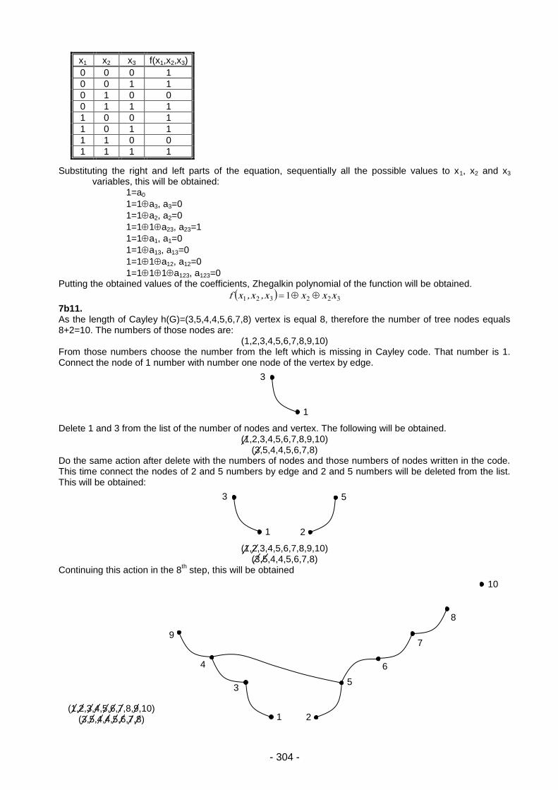
- 304 -
x1 x2 x3 f(x1,x2,x3)
0 0 0 1
0 0 1 1
0 1 0 0
0 1 1 1
1 0 0 1
1 0 1 1
1 1 0 0
1 1 1 1
Substituting the right and left parts of the equation, sequentially all the possible values to x1, x2 and x3 variables, this will be obtained:
1=a0
1=1a3, a3=0
1=1a2, a2=0
1=11a23, a23=1
1=1a1, a1=0
1=1a13, a13=0
1=11a12, a12=0
1=111a123, a123=0 Putting the obtained values of the coefficients, Zhegalkin polynomial of the function will be obtained.
322321 1 xxxx,x,xf
7b11. As the length of Cayley h(G)=(3,5,4,4,5,6,7,8) vertex is equal 8, therefore the number of tree nodes equals 8+2=10. The numbers of those nodes are:
(1,2,3,4,5,6,7,8,9,10) From those numbers choose the number from the left which is missing in Cayley code. That number is 1. Connect the node of 1 number with number one node of the vertex by edge.
Delete 1 and 3 from the list of the number of nodes and vertex. The following will be obtained.
(1,2,3,4,5,6,7,8,9,10) (3,5,4,4,5,6,7,8)
Do the same action after delete with the numbers of nodes and those numbers of nodes written in the code. This time connect the nodes of 2 and 5 numbers by edge and 2 and 5 numbers will be deleted from the list. This will be obtained:
(1,2,3,4,5,6,7,8,9,10)
(3,5,4,4,5,6,7,8) Continuing this action in the 8
th step, this will be obtained
3
1
5
2
4
9
6
7
8
10
(1,2,3,4,5,6,7,8,9,10) (3,5,4,4,5,6,7,8)
3
1
5
2
3
1
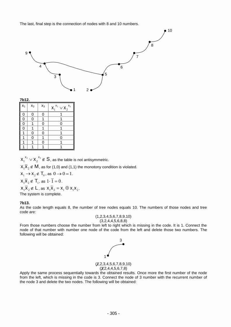
- 305 -
The last, final step is the connection of nodes with 8 and 10 numbers. 7b12.
x1 x2 x3 32
21
xxxx
0 0 0 1
0 0 1 1
0 1 0 0
0 1 1 1
1 0 0 1
1 0 1 0
1 1 0 1
1 1 1 1
Sxxxx 32
21 , as the table is not antisymmetric.
Mxx 21 , as for (1,0) and (1,1) the monotony condition is violated.
021 Txx , as 100 .
121 Txx , as 011 .
Lxx 21 , as 21121 xxxxx .
The system is complete. 7b13. As the code length equals 8, the number of tree nodes equals 10. The numbers of those nodes and tree code are:
(1,2,3,4,5,6,7,8,9,10) (3,2,4,4,5,6,8,8)
From those numbers choose the number from left to right which is missing in the code. It is 1. Connect the node of that number with number one node of the code from the left and delete those two numbers. The following will be obtained:
(1,2,3,4,5,6,7,8,9,10)
(3,2,4,4,5,6,7,8) Apply the same process sequentially towards the obtained results. Once more the first number of the node from the left, which is missing in the code is 3. Connect the node of 3 number with the recurrent number of the node 3 and delete the two nodes. The following will be obtained:
3
1
3
1
5
2
4
9
6
7
8
10
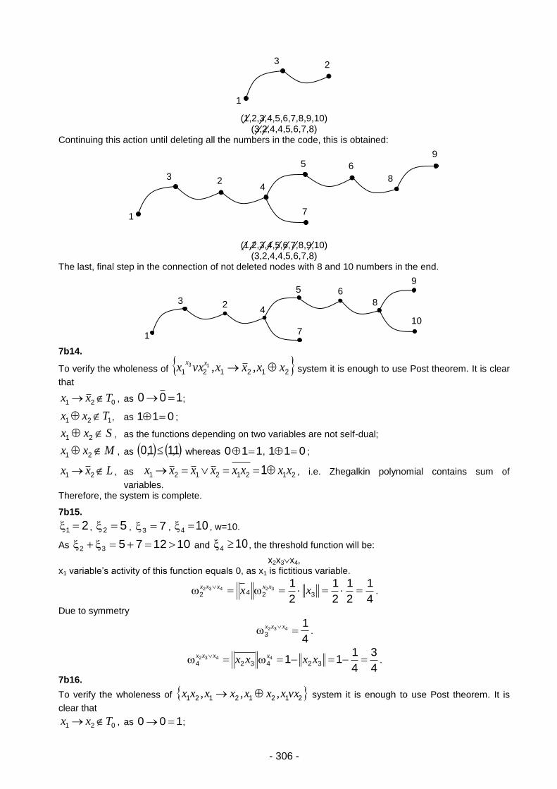
- 306 -
(1,2,3,4,5,6,7,8,9,10)
(3,2,4,4,5,6,7,8) Continuing this action until deleting all the numbers in the code, this is obtained:
(1,2,3,4,5,6,7,8,9,10) (3,2,4,4,5,6,7,8)
The last, final step in the connection of not deleted nodes with 8 and 10 numbers in the end.
7b14.
To verify the wholeness of 21212113 xx,xx,vxx
xx system it is enough to use Post theorem. It is clear
that
021 Txx , as 100 ;
121 Txx , as 011 ;
Sxx 21 , as the functions depending on two variables are not self-dual;
Mxx 21 , as 1110 ,, whereas 110 , 011 ;
Lxx 21 , as 21212121 1 xxxxxxxx , i.e. Zhegalkin polynomial contains sum of
variables. Therefore, the system is complete.
7b15.
21 , 52 , 73 , 104 , w=10.
As 10127532 and 104 , the threshold function will be:
x2x3x4, x1 variable’s activity of this function equals 0, as x1 is fictitious variable.
4
1
2
1
2
1
2
13242
32432
xxxxxxx
.
Due to symmetry
4
1432
3 xxx
.
4
3
4
111 324324
4432
xxxxxxxx
.
7b16.
To verify the wholeness of 21212121 vxx,xx,xx,xx system it is enough to use Post theorem. It is
clear that
021 Txx , as 100 ;
2 3
1
4
5 6
8
9
7 10
2 3
1
4
5 6
8
9
7
2 3
1
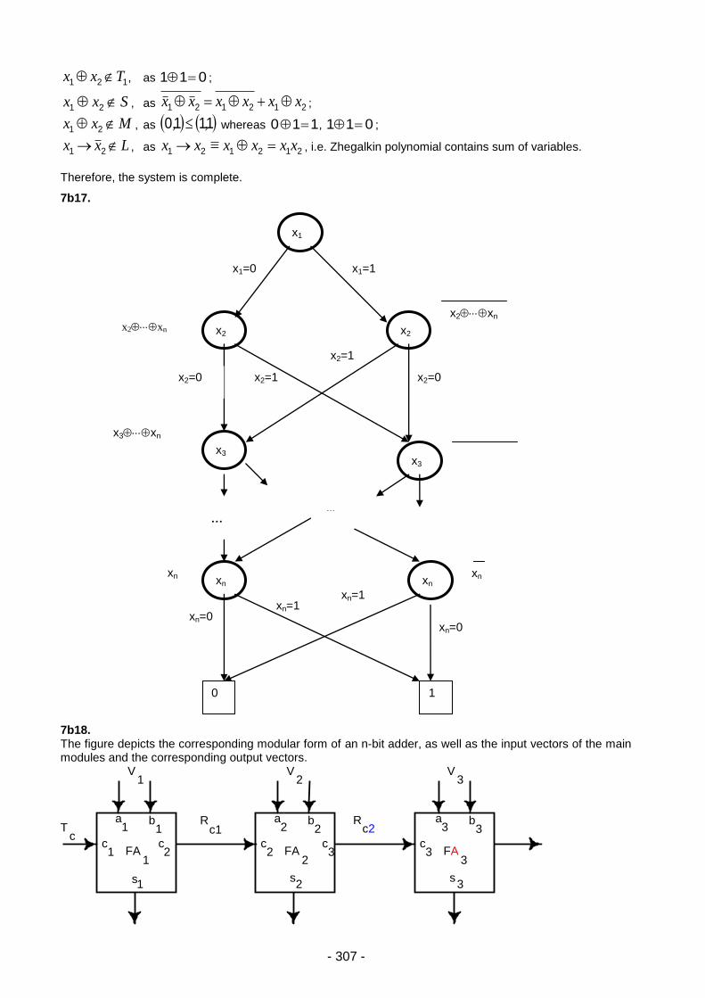
- 307 -
121 Txx , as 011 ;
Sxx 21 , as 212121 xxxxxx ;
Mxx 21 , as 1110 ,, whereas 110 , 011 ;
Lxx 21 , as 212121 xxxxxx , i.e. Zhegalkin polynomial contains sum of variables.
Therefore, the system is complete.
7b17. 7b18. The figure depicts the corresponding modular form of an n-bit adder, as well as the input vectors of the main modules and the corresponding output vectors.
FA 1
FA 2
FA 3
R c1
R c2
a 1
b 1
s 1
c 1
V 1
a 2
b 2
s 2
c 2
V 2
a 3
b 3
s 3
c 3
V 3
c 3
c 2
T c
xn=1
xn=0
xn=1 xn=0
x2=0
x2=1
x2=1
x1=0 x1=1
x1
x2 x2
x2xn
x2xn
x2=0
0 1
x3 x3
xn xn
…
…
x3xn
xn xn
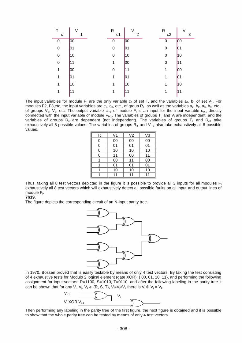
- 308 -
The input variables for module F1 are the only variable c1 of set Tc and the variables a1, b1 of set V1. For modules F2, F3,etc, the input variables are c2, c3, etc., of group Rc, as well as the variables a2, b2, a3, b3, etc., of groups V2, V3, etc. The output variable ci+1 of module Fi is an input for the input variable ci+1 directly connected with the input variable of module Fi+1. The variables of groups Tc and Vi are independent, and the variables of groups Rc are dependent (not independent). The variables of groups Tc and Rc1 take exhaustively all 8 possible values. The variables of groups Rci and Vi+1 also take exhaustively all 8 possible values.
Tc V1 V2 V3
0 00 00 00
0 01 01 01
0 10 10 10
0 11 00 11
1 00 11 00
1 01 01 01
1 10 10 10
1 11 11 11
Thus, taking all 8 test vectors depicted in the figure it is possible to provide all 3 inputs for all modules Fi
exhaustively all 8 test vectors which will exhaustively detect all possible faults on all input and output lines of module Fi. 7b19. The figure depicts the corresponding circuit of an N-input parity tree.
In 1970, Bossen proved that is easily testable by means of only 4 test vectors. By taking the test consisting of 4 exhaustive tests for Modulo 2 logical element (gate XOR): { 00, 01, 10, 11}, and performing the following assignment for input vectors: R=1100, S=1010, T=0110, and after the following labeling in the parity tree it
can be shown that for any Vi, Vj, Vk {R, S, T}, ViVjVk there is Vi Vj = Vk. Then performing any labeling in the parity tree of the first figure, the next figure is obtained and it is possible to show that the whole parity tree can be tested by means of only 4 test vectors.
0 00
0 01
0 10
1 00
0 11
1 01
1 10
1 11
R c1
V 2
0 00
0 01
0 10
0 11
1 00
1 01
1 10
1 11
T c
V 1
0 00
0 01
0 10
0 11
1 00
1 01
1 10
1 11
R c2
V 3
Vi XOR Vi-1
Vi-1 Vi
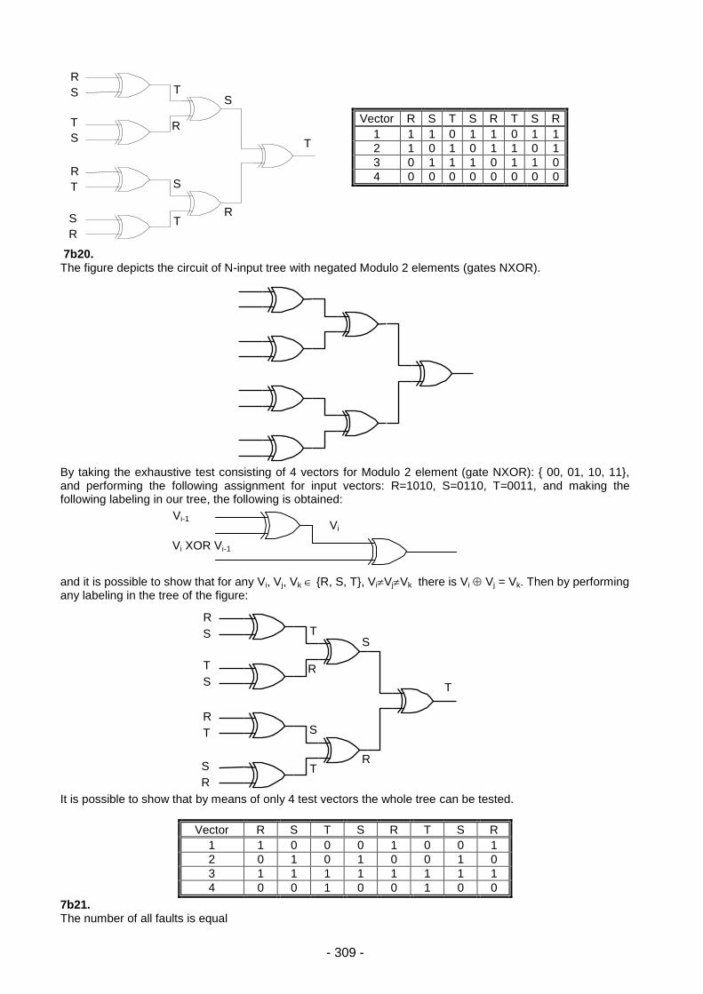
- 309 -
Vector R S T S R T S R
1 1 1 0 1 1 0 1 1
2 1 0 1 0 1 1 0 1
3 0 1 1 1 0 1 1 0
4 0 0 0 0 0 0 0 0
7b20. The figure depicts the circuit of N-input tree with negated Modulo 2 elements (gates NXOR).
By taking the exhaustive test consisting of 4 vectors for Modulo 2 element (gate NXOR): { 00, 01, 10, 11}, and performing the following assignment for input vectors: R=1010, S=0110, T=0011, and making the following labeling in our tree, the following is obtained:
and it is possible to show that for any Vi, Vj, Vk {R, S, T}, ViVjVk there is Vi Vj = Vk. Then by performing any labeling in the tree of the figure: It is possible to show that by means of only 4 test vectors the whole tree can be tested.
Vector R S T S R T S R
1 1 0 0 0 1 0 0 1
2 0 1 0 1 0 0 1 0
3 1 1 1 1 1 1 1 1
4 0 0 1 0 0 1 0 0
7b21. The number of all faults is equal
R
S
T
S
R
T
S
R
T S
R
S
T R
T
Vi XOR Vi-1
Vi-1 Vi
R
S
T
S
R
T
S
R
T S
R
S
T R
T
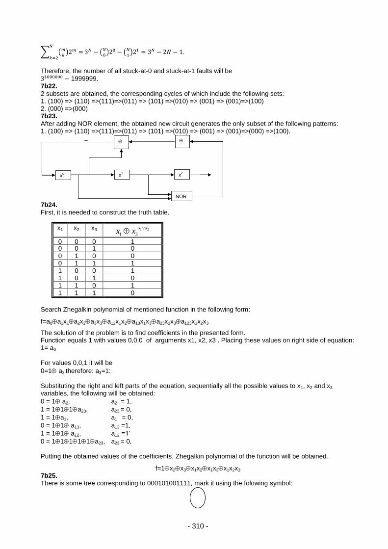
- 310 -
∑ ( )
(
) (
) .
Therefore, the number of all stuck-at-0 and stuck-at-1 faults will be
1999999. 7b22. 2 subsets are obtained, the corresponding cycles of which include the following sets: 1. (100) => (110) =>(111)=>(011) => (101) =>(010) => (001) => (001)=>(100) 2. (000) =>(000) 7b23. After adding NOR element, the obtained new circuit generates the only subset of the following patterns: 1. (100) => (110) =>(111)=>(011) => (101) =>(010) => (001) => (001)=>(000) =>(100).
7b24. First, it is needed to construct the truth table.
x1 x2 x3 21
31
xxxx
0 0 0 1 0 0 1 0 0 1 0 0 0 1 1 1 1 0 0 1 1 0 1 0 1 1 0 1 1 1 1 0
Search Zhegalkin polynomial of mentioned function in the following form:
f=a0a1x1a2x2a3x3a12x1x2a13x1x3a23x2x3a123x1x2x3
The solution of the problem is to find coefficients in the presented form. Function equals 1 with values 0,0,0 of arguments x1, x2, x3 . Placing these values on right side of equation: 1= a0
For values 0,0,1 it will be
0=1 a3 therefore: a3=1: Substituting the right and left parts of the equation, sequentially all the possible values to x1, x2 and x3 variables, the following will be obtained:
0 = 1 a2, a2 = 1,
1 = 111a23, a23 = 0,
1 = 1a1, a1 = 0,
0 = 11 a13, a13 =1,
1 = 11 a12, a12 =1’
0 = 11111a23, a23 = 0, Putting the obtained values of the coefficients, Zhegalkin polynomial of the function will be obtained.
f=1x2x3x1x2x1x3x1x2x3
7b25. There is some tree corresponding to 000101001111, mark it using the folowing symbol:
x0
NOR
x1 x
2
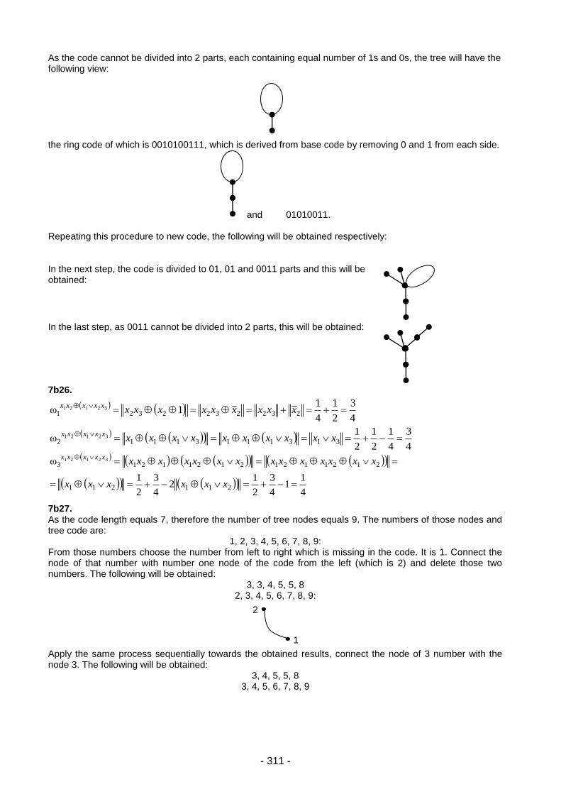
- 311 -
As the code cannot be divided into 2 parts, each containing equal number of 1s and 0s, the tree will have the following view:
the ring code of which is 0010100111, which is derived from base code by removing 0 and 1 from each side.
and 01010011.
Repeating this procedure to new code, the following will be obtained respectively: In the next step, the code is divided to 01, 01 and 0011 parts and this will be obtained:
In the last step, as 0011 cannot be divided into 2 parts, this will be obtained:
7b26.
4
3
2
1
4
11ω 2322322321
32121
xxxxxxxxxxxxxx
4
3
4
1
2
1
2
1ω 31311131112
32121
xxxxxxxxxxxxxxx
4
11
4
3
2
12
4
3
2
1
ω
211211
21211212121121332121
xxxxxx
xxxxxxxxxxxxxxxxxxx
7b27. As the code length equals 7, therefore the number of tree nodes equals 9. The numbers of those nodes and tree code are:
1, 2, 3, 4, 5, 6, 7, 8, 9: From those numbers choose the number from left to right which is missing in the code. It is 1. Connect the node of that number with number one node of the code from the left (which is 2) and delete those two numbers. The following will be obtained:
3, 3, 4, 5, 5, 8 2, 3, 4, 5, 6, 7, 8, 9:
Apply the same process sequentially towards the obtained results, connect the node of 3 number with the node 3. The following will be obtained:
3, 4, 5, 5, 8 3, 4, 5, 6, 7, 8, 9
2
1
- 312 -
Continuing this action until deleting all the numbers in the code, this is sequentially obtained:
4, 5, 5, 8 3, 4, 5, 7, 8, 9
5, 5, 8 4, 5, 7, 8, 9
5, 8 5, 7, 8, 9
8 5, 8, 9
8, 9
Finally, the remaining 8 and 9 nodes are connected to each
other.
7b28. Let F1 be the fault “line A stuck-at-1”, F2 be “line B stuck-at-1” and F3 be “line Z* be stuck-at-1”. Then it is easy to check that F1 = F2 = F3 since F1={(00)}, F2={(00)}, F3={(00)}. 7b29. According to McCluskey, the number of input patterns for the pseudoexhaustive test is 2
n1 + 2
n2 + … + 2
n5=
212
+ 214
+ 216
+ 218
+ 2
20 = 2
12(1+4+16+64+256) = 341. 2
12= 1396736.
7b30. Since T(F1)={(0,0)}, T(F2)={(0,0)}, T(F3)={(0,0)}, then T(F1) = T(F2) = T(F3). 7b31. Denote by F1 the fault ”line A stuck-at-0”, F2 – “line B stuck-at-0” and F3 – “line Z stuck-at-0”. Prove that single faults F1, F2 and F3 are equivalent.
Since T(F1)={(1,1)}, T(F2)={(1,1)}, T(F3)={(1,1)}, then T(F1) = T(F2) = T(F3). 7b32. Search strategy is the following:
1) Starting from the 2nd
vertex, go deeper in any path as it is still possible. 2) Return by searching other paths. 3) Repeat the 1
st and the 2
nd steps until detecting all possible vertices.
5
2
1
3 6
4
7
8
9 5
2
1
3 6
4
7 8
5
2
1
3 6
4
7
5
2
1
3 6
4
2
3 6
4
1
2
1
3 6
2
1
3
- 313 -
4) If there are still undetected vertices, select one of them and repeat 1-3 steps. 5) Repeat 1-4 steps until detecting all the vertices of the graph.
Mark the numbers of detection and completion steps on vertices. Answer
7b33. Separate strongly connected components in the given directed graph. Solution:
1) Search according to depth starting with any vertex. 2) Construct the transported graph of the given graph. 3) Search according to depth in transported graph. In each cycle, start from the vertex with the highest
value of process completion.
Each search cycle will separate strongly connected components. Answer: Observe the solution on the previous example.
In the previous example, the completions of vertex processing according to decrease are the following: 5, 1, 2, 6, 7, 3, 4, 8. Therefore the search will start from 5
th vertex.
The strongly connected components will be a) 5; b) 1; c) 2; d) 3, 4, 6, 7; e) 8 7b34. 1) Search according to density, starting from any vertex. 2) Classify the vertices from left to right, according to the decrease of ends of vertex processing.
Answer
5/6 4/7 3/10 2/11
16/17 8/9 13/14
1/15
1
2 3
5 6
4
7 8
15/16
12/13
7/14 1/2
9/10
8/11
5/6 3/4
1
2 3
5 6
4
7 8
4/5 9/10 8/11 13/16
3/6 2/7 1/12 14/15
1
2 3
5 6
4
7 8
4
1
2
5
6
3
7
8
- 314 -
7b35. The objective function will be f = 2f1 + f2. Answer:
7 5 6 7 8 9 10 11
6 4 5 6 7 8 11 12
5 3 6 7 9 12 11 B
4 2 3 4 8 11 10
3 1 2 3 6 7 9
2 0
1 2 5 6 7 8
1 1 2 3 6 7 9
1 2 3 4 5 6 7
7b36. The matrix of orthogonal distances is built, calculating the orthogonal distance between contacts.
la,b = | 2-8 | + | 9-8 | = 7; lac = 4; lad=13; lae = 7: lbc = 9; lbd = 5; lbe = 12; lcd = 8; lce = 3; lde = 7
The matrix will have the following view:
a b c d e
a 0 7 v 4 v 12 7
b 7 0 9 5 v 12
c 4 9 0 8 3 v
d 12 5 8 0 7
e 7 12 3 7 0
2 3 1
d b a c e
Answer:
9
8
7
6
5
4
3
2
1
1 2 3 4 5 6 7 8 9
7b37. The adjacency matrix and the solution process are the following:
1 2 3 4 5 6 f0 f1
1 0 1 0 2 1 0 4 X X
2 1 0 1 0 0 2 4 2 2
3 0 1 0 1 0 0 2 2 0 X
e(2,2)
c(2,5)
a(2,9)
b(8,8)
d(8,3)
- 315 -
4 2 0 1 0 0 0 3 -1 X
5 1 0 0 0 0 2 3 1 1
6 0 2 0 0 2 0 4 4 4
Answer: 1
st group - 1, 3, 4;
2nd
group - 2, 5, 6. 7b38.
The adjacency matrix and the solution process are the following:
l1 l2 l3 l4 l5 f0 f1 f2 f3 f4
l1 0 0 1 1 0 2 X X X X
l2 0 0 1 1 0 2 2 0 X X
l3 1 1 0 0 1 3 1 X X X
l4 1 1 0 0 1 3 1 1 -1 X
l5 0 0 1 1 0 2 2 0 0
Answer: l1 l3 l2 l4 l5
7b39. Timing graph and calculation process are the following:
Answer: The critical paths are two and have 70 unit of delay. a) 5 6 3 4 b) 5 6 3 7 7b40. See the solution of 7b24. 7b41. See the solution of 7b25. 7b42. See the solution of 7b26. 7b43.
f(x1,x2,x3)= x1,x2 x3, as 5721
and .563 Construct the table for perfect
disjunctive normal form of the function. x1 x2 x3 x1 x2 x3
0 0 0 0
0 0 1 1
0 1 0 0
0 1 1 1
1 0 0 0
1 0 1 1
1 1 0 1
1 1 1 1
C2
10
C3
5
C5
20
C6
30
C7
30
C7
30
C7
30
C6
30
C4
30
C6
30
C4
30
C1
5
70/70
30/40
5/20 0/15
10/10
0/0
70/70
40/40
5/10
0/5
1
2
3
5 6
4
7
8 9
10
- 316 -
Perfect disjunctive normal form of the function will be:
321321321321321321 xxxxxxxxxxxxxxxx,x,xf
7b44.
To check the completeness of the system, use Post theorem. It is obvious that 21 xx function preserves 0
constant 00100 . The other functions of the system also preserve 0 constant: 0•0=0 and 00=0. Therefore, the system is fully included in the class that preserves 0 constant functions. Hence, according to Post theorem, it follows that the system is not complete.
7b45. Zhegalkin polynomial is searched in the form of indefinite coefficients:
3211233223311321123322110321xxxaxxaxxaxxaxaxaxaa)x,x,x(f
The table of the function looks as follows:
X1 X2 X3 F(x1,x2,x3)
0 0 0 1
0 0 1 1
0 1 0 0
0 1 1 0
1 0 0 1
1 0 1 0
1 1 0 1
1 1 1 1
On the right and left parts of the equation, giving the mentioned values to x1, x2 and x3 variables sequentially, the following will be obtained:
1a,a11111
1a,a111
1a,a10
0a,a11
0a,a110
1a,a10
0a,a11
a1
123123
1212
1313
11
3232
22
33
0
Putting the obtained values of the coefficients in the formula, presented by indefinite coefficients, Zhegalkin polynomial of the function will be obtained:
32131212321xxxxxxxx1)x,x,x(f
7b46.
2
1
4
1
4
1
2
1xxx2xxx)xxx()11()xxx(
432432432432
)xxx()xx(
1
43121
2
1x)xxx(x)xxx(1
14311431
)xxx()xx(
2
43121
4
11
2
1
4
3
x2xxxx)xx(x)xx()xx()xx(11411411214121
)xxx()xx(
3
43121
4
11
4
3
2
1
x2xxx)xx(x)xx()xx(x)xx(13113113121121
)xxx()xx(
4
43121
7b47.
It is clear that 0
x
2
x
1Txx 13 and 1T
2x1x . It is also clear that ,Sxx
21 as no function of two variables
is self-dual. Then ,Mxx21 as (0,1) precedes (1,1), but 110 and ,011 i.e. the monotony condition
- 317 -
is violated, therefore M2x1x . It is also obvious that L2x1x . Therefore, according to Post’s
theorem, the mentioned system is complete.
7b48.
It is obvious that the threshold function with ,4,3,2321 4w parameters has
321xxx
formula, as W21 and W3 .
4
11
4
3
2
1x2
4
3
2
1
)xx(x2xxx)xx(x)xxx()xxx(
3
323323323321321
xxx
1
321
Due to symmetry it is clear that 4
1xxx2 321 .
.4
3
4
11x
32x1xxxx3 3321
7b49.
As ,5,4,3,24321 W=8 and ,W,W,W
3214342 the threshold
function will have the following disjunctive normal form:
3x2x1x4x3x4x2x .
As ,abbaba Zhegalkin polynomial of the obtained function will be got in the following way:
43213214324342432143214321
321432434232143243423214342
xxxxxxxxxxxxxxxxxxxxxxxxxx
xxxxxxxxxxxxxxxxxxxxxxxxxxx
7b50. Some tree corresponds to 000100011111, which is conventionally denoted by
symbol. As the code cannot be divided into 2 such parts each of which containing equal number of 0s and
1s, it would have the following view: the code of
part of the ring would be 0010001111. It is obtained from the main code by removing 0 and 1 from its left and
right.
Performing the same action towards the obtained new code, the following will be obtained correspondingly:
and 01000111.
In the next step the code is divided into 01 and 000111 parts and the following is obtained:
In the recurrent step 000111 is not divided into 2 parts, therefore the following result will be obtained:
and 0011.
- 318 -
Continuing, the following will be obtained:
and 0011
as 0011 is not divided into 2 parts. Finally, final result will be in the last step: 7b51. All the solutions should satisfy the following equation:
g(x)df(x,g(x))/dg(x)=g(x)[f(x,g=0) f(x,g=1)]=g(x)(x3 1) = xxx 321 = 1:
The equation has only one solution - T = {(110)}. 7b52. All the solutions should satisfy the following equation:
)x(g df(x,g(x))/dg(x) = )x(g [f(x,g=0) f(x,g=1)] = )x(g (x3 1) = xxx 321)( = xxxx 3231
= 1.
The equation has three solutions, i.e. T = {(000), (010),(100)}. 7b53. The number of all possible, two and more, faults equals to
S = 1N21N2 3C2C2Nm
N
N
0m
mm
N
N
2m
m
. 7b54. The number of all possible, three and more, faults equals to
S = 1N5,22N3C2C2C22N
1
0m
m
N
mm
N
N
0m
mm
N
N
2m
m
. 7b55. The recalculation coefficient of the counter is equal to 5. The output of NOR cell functions as the 5
th output.
When pulses are given from generator, logic 1 moves through 5 outputs of the counter. Appearance of logic 1 in 0, 1, 2, 4 and 8 outputs of the decoder corresponds to the states of the counter. Therefore, the pulse frequency in the 2
nd output of the decoder will be 5 times smaller than the frequency of the generator.
7b56. The given logic function is represented in Perfect Disjunctive Normal Form (DNF) and takes 1 value for three sets of A, B, C input variables - sixth, fifth and third (the numbers of sets are obtained by means of summation of weight coefficients of address inputs of multiplexers that correspond to direct values of variables. Logic zeros should be given to those information inputs of multiplexers because the function is formed in inverse output. Therefore the answer will be 10010111. 7b57. By summing 48H and 29H numbers, given to A and B inputs of the circuit, 48H+29H=71H number will be obtained in the output of the adder. High rank of the obtained number will be given to the left indicator from internal decoder, and low rank – to the right indicator. Thus, number 71 will be depicted on the indicator. 7b58. The adjacency matrix of the given circuit and solution process is shown in the table.
e1 e2 e3 e4 e5 f0 f1 f2 f3 f4
e1 - 1 0 0 0 1 X X X X
e2 1 - 1 2 0 4 4-2*1=2 X X X
e3 0 1 - 2 1 4 4-2*0=4 4-2*1=2 2-2*2=-2 X
e4 0 2 2 - 1 5 5-2*0=5 5-2*2=1 X X
e5 0 0 1 1 - 2 2-2*0=2 2-2*0=2 2-2*1=0
The element with maximum connections with already selected elements and minimum connections with not yet selected elements is chosen in each step. This is the key requirement for calculation. The calculation is carried out by the following recurrent formula: fij=f(i-1)j-2*rjk,

- 319 -
where fij is f pretender function value in i-th step of calculation for j-th element. rjk is the number of connections of j-th element with k-th element, selected in (i-1)-th step. As a recurrent element, the element with min fij is chosen in each step. If they are more than one, anyone can be chosen. As seen from the table, initial row placement of the given circuit will have the following sequence: e1 →e2→ e4 →e3→ e5. 7b59. Build the graph of horizontal and vertical constraints of a, b, c, d, e, f nets. Build the combined graph and heuristically define its chromatic number as shown in the figure below. Besides, bottom-up numbering of horizontal paths is conditional. Hence it follows that the numbers in the beginning of directed edges that correspond to vertical constraints should be smaller than the numbers in the end of the edges.
As seen from the figure, the chromatic number of the graph is equal to 4. Hence it follows that at least 4 horizontal channels are needed for two-layer orthogonal mounting of the given nets.
7b60. Data Flow Graph of the circuit is shown in the figure. The earliest times of data appearance are shown on the edges. As seen from the figure, there is signal racing in the inputs of C2 and C4 elements with 3 and 2 c.u. sizes respectively. Therefore to exclude signals racing, delay elements are to be added before corresponding inputs.
The functional circuit of the device together with delay elements is shown in the figure. t1and t2 delay elements are with 3 c.u. and 2 c.u. respectively.
C1
b
c
d
e
0
0
0
0
3
3
5
C3
C2
C4
a
y
0
a e a d c f
a f b b e d c
3
4
2
1
a) A graph of horizontal constraints
b) A graph of vertical constraints
c) A combined graph
d
c
f
b
e
a
d
c
f
b
e
a
1 4 d
c
f
b
e
a
2
2
1
3
- 320 -
7b61. The functional circuit without using multiplexers, will be:
The operating cycles of the circuit and the actions, taken at each cycle are presented in the table.
Functional unit
Quantity Cycle 1 Cycle 2 Cycle 3
3 r1=a*b, r2=d*e
- y=r2*r3
1 - r3=r1+c -
The functional circuit after optimization, using multiplexers, will be:
The operating cycles of the optimized circuit and the actions, taken at each cycle are presented in the table.
Functional unit
Quantity Cycle 1 Cycle 2 Cycle 3
1 r1=a*b r2=d*e y=r2*r3
1 - r3=r1+c -
t1
t2
a
b
c
d
e
y
a
b
c
d
e
y
r1
r2
r3
a
d r2
b
e r3
y
r1
c
r3
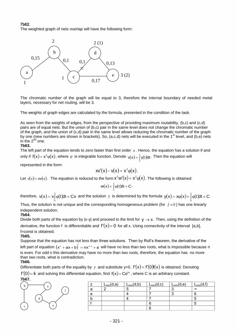
- 321 -
7b62. The weighted graph of nets overlap will have the following form:
The chromatic number of the graph will be equal to 3, therefore the internal boundary of needed metal layers, necessary for net routing, will be 3.
The weights of graph edges are calculated by the formula, presented in the condition of the task.
As seen from the weights of edges, from the perspective of providing maximum routability, (b,c) and (c,d) pairs are of equal nets. But the union of (b,c) pair in the same level does not change the chromatic number of the graph, and the union of (c,d) pair in the same level allows reducing the chromatic number of the graph by one (new numbers are shown in brackets). So, (a,c,d) nets will be executed in the 1
st level, and (b,e) nets
in the 2nd
one. 7b63.
The left part of the equation tends to zero faster than first order x . Hence, the equation has a solution if and
only if xxxf 2 , where is integrable function. Denote x
0
dttyxv . Then the equation will
represented in the form:
xxxvxvx 2 .
Let xxwxv . The equation is reduced to the form xxxwx 22 . The following is obtained:
Cdttxwx
0
,
therefore, Cxdttxxvx
0
and the solution y is determined by the formula Cdttxxxyx
0
.
Thus, the solution is not unique and the corresponding homogeneous problem (for 0f ) has one linearly
independent solution. 7b64. Divide both parts of the equation by |x-y| and proceed to the limit for xy . Then, using the definition of the
derivative, the function f is differentiable and 0xf for all x. Using connectivity of the interval [a,b],
f=const is obtained.
7b65. Suppose that the equation has not less than three solutions. Then by Roll’s theorem, the derivative of the
left part of equation anxbaxx 1nn
will have no less than two roots, what is impossible because n
is even. For odd n this derivative may have no more than two roots, therefore, the equation has no more than two roots, what is contradiction. 7b66.
Differentiate both parts of the equality by y and substitute y=0. xf0fxf is obtained. Denoting
k0f and solving this differential equation, find kxCexf , where C is an arbitrary constant.
7b67.
z Lmin(d,a) Lmin(d,b) Lmin(d,c) Lmin(d,e) Lmin(d,f)
a 2 5 7 3 ∞
e 4 7 3 6
b 4 7 5
f 6 5
6 c
b
d
f
e
a
a
b
c
d
e
2
1
2 (1)
3 (2) 1
0,15 0,1
0,17
0,13 0,1
≈
- 322 -
7b68.
7b69. The sensitive path is marked with red in the figure below.
7b70.
7b71. The initial set of faults is: {a/0, a/1, b/0, b/1, c/0, c/1, d/0, d/1, e/0, e/1, f/0, f/1, g/0, g/1, h/0, h/1, i/0, i/1, j/0, j/1, k/0, k/1, z/0, z/1}: According to the mentioned theorem, the test set of mentioned type can be restricted by considering the corresponding faults on checkpoints. After reduction the following set of faults is obtained; {a/0, a/1, b/0, b/1, c/0, c/1, d/0, d/1, e/0, e/1, , f/0, f/1, h/0, h/1, i/0, i/1}: Thus, instead of consideration of the initial set of 28 faults, only 16 is considered. The initial set is reduced by 57.14 %. 7b72. (1, 1, 1) and (0, 0, 0) 7b73.
As the given expression can be substituted by the following equivalent expression: C⋅ (A+B) ՛ =C⋅ A ՛ ⋅ B ՛, it is obvious that the answer should be the part of cycle C which excludes parts, belonging to cycles A and B. So the answer is the 7
th segment.
7b74. The timing graph of the circuit will have this form:
1 0 0 1
4 3 2 1 0 0 0 0 0 0 0 0 0 1 2 3 4 5
y 4 3 2 2 1 1 1 1 1 1 1
5 4 2 2 2 2 2 3 4 5 6
3 3 3 3 3 4 5 6 7
4 4 4 7 8
5 5 5 8 9 10
6 6 6 11 10 9 10 11
7 12
8 13
9 14
10 11 12 13 14
11 12 13 14
4 8 12 16 20 x
D
SA1
{0,0,D} {0,1,D} {1,0,D}
PDCF PDCF PDCF 1 0 0
0 1 0
A
B
C
E
sa0
f
g
h
i j
k L
0
1
1
1
D D D
D D 0
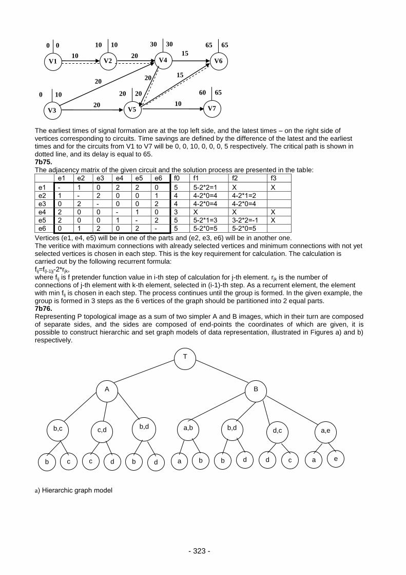
- 323 -
The earliest times of signal formation are at the top left side, and the latest times – on the right side of vertices corresponding to circuits. Time savings are defined by the difference of the latest and the earliest times and for the circuits from V1 to V7 will be 0, 0, 10, 0, 0, 0, 5 respectively. The critical path is shown in dotted line, and its delay is equal to 65. 7b75. The adjacency matrix of the given circuit and the solution process are presented in the table:
e1 e2 e3 e4 e5 e6 f0 f1 f2 f3
e1 - 1 0 2 2 0 5 5-2*2=1 X X
e2 1 - 2 0 0 1 4 4-2*0=4 4-2*1=2
e3 0 2 - 0 0 2 4 4-2*0=4 4-2*0=4
e4 2 0 0 - 1 0 3 X X X
e5 2 0 0 1 - 2 5 5-2*1=3 3-2*2=-1 X
e6 0 1 2 0 2 - 5 5-2*0=5 5-2*0=5
Vertices (e1, e4, e5) will be in one of the parts and (e2, e3, e6) will be in another one. The veritice with maximum connections with already selected vertices and minimum connections with not yet selected vertices is chosen in each step. This is the key requirement for calculation. The calculation is carried out by the following recurrent formula: fij=f(i-1)j-2*rjk, where fij is f pretender function value in i-th step of calculation for j-th element. rjk is the number of connections of j-th element with k-th element, selected in (i-1)-th step. As a recurrent element, the element with min fij is chosen in each step. The process continues until the group is formed. In the given example, the group is formed in 3 steps as the 6 vertices of the graph should be partitioned into 2 equal parts. 7b76. Representing P topological image as a sum of two simpler A and B images, which in their turn are composed of separate sides, and the sides are composed of end-points the coordinates of which are given, it is possible to construct hierarchic and set graph models of data representation, illustrated in Figures a) and b) respectively.
a) Hierarchic graph model
A
T
b,c a,e
B
c,d b,d a,b b,d d,c
e b c c d b d a d a b b d c
20
15
20
10
10
15
20
0
0
V1
10
10
V2
10
0
V3
20
20
V5
30
30
V4
65
60
V7
65
65
V6
20
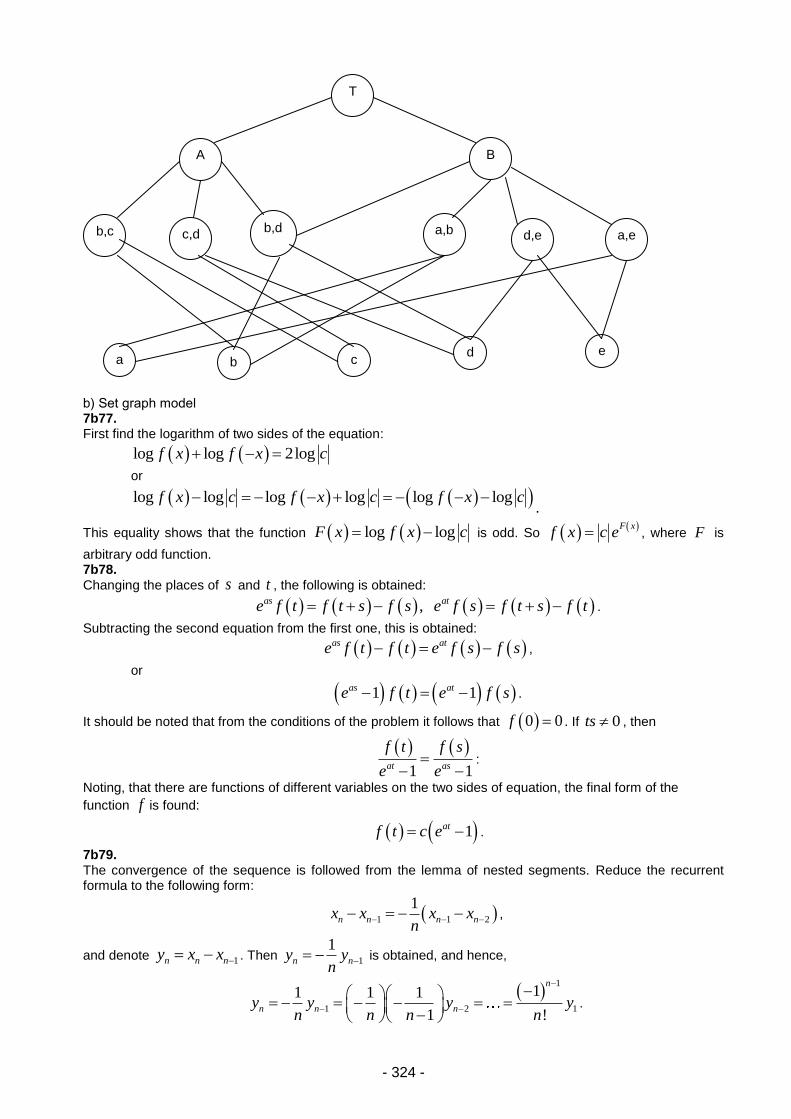
- 324 -
b) Set graph model 7b77. First find the logarithm of two sides of the equation:
log log 2logf x f x c
or
log log log log log logf x c f x c f x c .
This equality shows that the function log logF x f x c is odd. So F xf x c e , where F is
arbitrary odd function. 7b78.
Changing the places of s and t , the following is obtained:
,as ate f t f t s f s e f s f t s f t .
Subtracting the second equation from the first one, this is obtained:
as ate f t f t e f s f s ,
or
1 1as ate f t e f s .
It should be noted that from the conditions of the problem it follows that 0 0f . If 0ts , then
1 1at as
f t f s
e e
:
Noting, that there are functions of different variables on the two sides of equation, the final form of the
function f is found:
1atf t c e .
7b79. The convergence of the sequence is followed from the lemma of nested segments. Reduce the recurrent formula to the following form:
1 1 2
1n n n nx x x x
n ,
and denote 1n n ny x x . Then 1
1n ny y
n is obtained, and hence,
1
1 2 1
11 1 1
1 !
n
n n ny y y yn n n n
.
A
T
b,c a,e
B
c,d b,d a,b d,e
c d
b a e
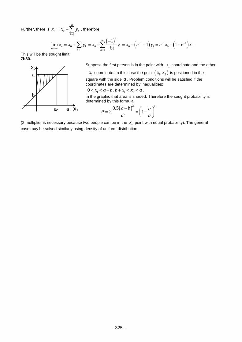
- 325 -
Further, there is 0
1
n
n k
k
x x y
, therefore
1 1 1
0 0 1 0 1 0 1
1 1
1lim 1 1
!
k
n kn
k k
x x y x y x e y e x e xk
.
This will be the sought limit. 7b80.
Suppose the first person is in the point with 1x coordinate and the other
- 2x coordinate. In this case the point 1 2,x x is positioned in the
square with the side a . Problem conditions will be satisfied if the
coordinates are determined by inequalities:
10 x a b , 1 2b x x a .
In the graphic that area is shaded. Therefore the sought probability is determined by this formula:
2 2
2
0.52 1
a b bP
a a
(2 multiplier is necessary because two people can be in the kx point with equal probability). The general
case may be solved similarly using density of uniform distribution.
a
b
a-b
a X1
X2
- 326 -
8. OBJECT-ORIENTED PROGRAMMING
a) Test questions
8a1. B 8a2. B 8a3. E 8a4. D 8a5. B 8a6. C 8a7. A 8a8. B 8a9. C 8a10. D 8a11. B 8a12. D 8a13. C 8a14. A 8a15. A 8a16. C 8a17. E 8a18. E 8a19. C 8a20. A 8a21. D 8a22. B 8a23. E 8a24. E 8a25. C 8a26. D 8a27. C 8a28. C 8a29. E 8a30. B 8a31. E 8a32. D 8a33. B 8a34. A 8a35. B 8a36. A 8a37. B
8a38. A 8a39. B 8a40. E 8a41. E 8a42. C 8a43. B 8a44. D 8a45. D 8a46. D 8a47. C 8a48. E 8a49. D 8a50. B 8a51. D 8a52. C 8a53. D 8a54. D 8a55. B 8a56. A 8a57. C 8a58. C 8a59. E 8a60. A 8a61. D 8a62. A 8a63. A 8a64 B 8a65. A 8a66. E 8a67 A 8a68 B 8a69 D 8a70 C 8a71 B 8a72 A 8a73 B 8a74 B
8a75. A 8a76. D 8a77. E 8a78. E 8a79. B 8a80. D 8a81. E 8a82. A 8a83. C 8a84. D 8a85. C 8a86. D 8a87. C 8a88. A 8a89. D 8a90. B 8a91. A 8a92. B 8a93. A 8a94. C 8a95. A 8a96. B 8a97. A 8a98. C 8a99. A 8a100. C 8a101. B 8a102. A 8a103. C 8a104. C 8a105. A 8a106. A 8a107. B 8a108. C 8a109. B 8a110. A

- 327 -
b) Problems 8b1. The length of the greatest common subsequence can be computed using the following program: #include <stdio.h>
#define N 1000
#define max(a,b) ((a>b) ? a : b)
int L[N][N];
int main(){
char a[N];
char b[N];
int i, j, n, m;
int yes = 0;
scanf("%s", a);
scanf("%s", b);
n = strlen(a);
m = strlen(b);
for( j = 0; j < m ; j++ ) {
if( b[j] == a[0] ) yes = 1;
L[0][j] = yes;
}
yes = 0;
for(i = 0; i < n; i++) {
if( a[i] == b[0] ) yes = 1;
L[i][0] = yes;
}
for(i = 1; i < n; i++) {
for(j = 1; j < m ; j++) {
if( a[i] == b[j] )
L[i][j] = L[i-1][j-1] + 1;
else
L[i][j] = max( L[i-1][j], L[i][j-1] );
}
}
printf( "%d\n", L[n-1][m-1] );
return 0;
}
8b2. AM(10,10)= 7368
8b3. Sum of digits =150 Q=3.752002426043100302699428993946639820.
8b4. Subs(n,k):=
If (n==k) then Ss={{1,2,3,...,n}};
goto END;
else A={1,...,k}
end;
Ss={};
p=k;
label P
Ss=SsA; If (A(k)==n) then p=p-1
else p=k
end;
If (p>=1) then i=k+1;
label Q;
i-i-1;
If(i>=p) then A(i)=A(p)+i-p+1;
goto Q
else goto P;
end;
end;
label END;
Rerurn(Ss)

- 328 -
8b5. Use Induction. The loop invariant is the following: xjyj
Zj = y0
z0
8b6. Use Induction.
8b7. Use Induction.
8b8. #include <iostream>
using namespace std;
int main(){
int n;
cin >> n;
cout << n - (n/2 + n/3 + n/5 - n/6 - n/15 - n/10 + n/30) << endl;
return 0;
}
8b9. #include <iostream>
#include <fstream>
#include <cmath>
#include <algorithm>
#include <set>
#include <queue>
#include <stack>
#include <iomanip>
using namespace std;
struct matric {
int a[2][2];
};
matric a1;
matric mul(matric a,matric b) {
int i,j,k;
matric h;
for (i=0;i<2;i++)
for (j=0;j<2;j++)
h.a[i][j]=0;
for (i=0;i<2;i++)
for (j=0;j<2;j++)
for (k=0;k<2;k++)
{
h.a[i][j]= ((__int64)h.a[i][j] + (__int64)a.a[i][k]*b.a[k][j])
% 1000007;
h.a[i][j]%=1000007;
}
return h;
}
matric stepen(matric a,int n) {
if (n==1)
return a;
matric h=stepen(a,n/2);
h=mul(h,h);
if (n&1)
h=mul(h,a1);
return h;
}
int main() {
int n;
cin >> n;
a1.a[0][0]=1;a1.a[0][1]=1;
a1.a[1][0]=1;a1.a[1][1]=0;
matric h1 = stepen(a1,n);
cout << h1.a[0][0] << endl;
return 0;
}
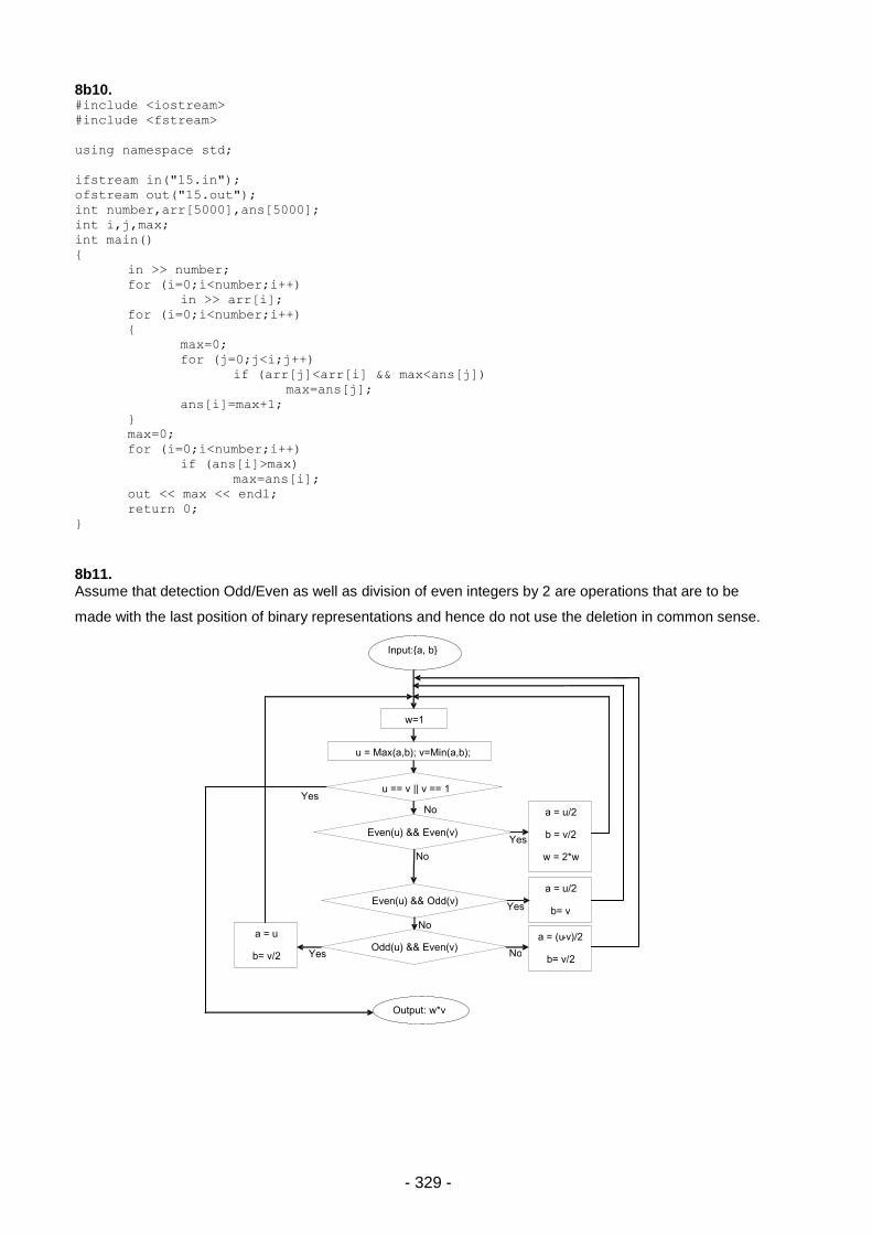
- 329 -
8b10. #include <iostream>
#include <fstream>
using namespace std;
ifstream in("15.in");
ofstream out("15.out");
int number,arr[5000],ans[5000];
int i,j,max;
int main()
{
in >> number;
for (i=0;i<number;i++)
in >> arr[i];
for (i=0;i<number;i++)
{
max=0;
for (j=0;j<i;j++)
if (arr[j]<arr[i] && max<ans[j])
max=ans[j];
ans[i]=max+1;
}
max=0;
for (i=0;i<number;i++)
if (ans[i]>max)
max=ans[i];
out << max << endl;
return 0;
}
8b11. Assume that detection Odd/Even as well as division of even integers by 2 are operations that are to be
made with the last position of binary representations and hence do not use the deletion in common sense.
Input:{a, b}
w=1
u = Max(a,b); v=Min(a,b);
u == v || v == 1
Even(u) && Even(v)
Even(u) && Odd(v)
Odd(u) && Even(v)
Output: w*v
a = u
b= v/2
a = u/2
b = v/2
w = 2*w
a = u/2
b= v
a = (u - v)/2
b= v/2
No
Yes
Yes
Yes
No Yes
No
No
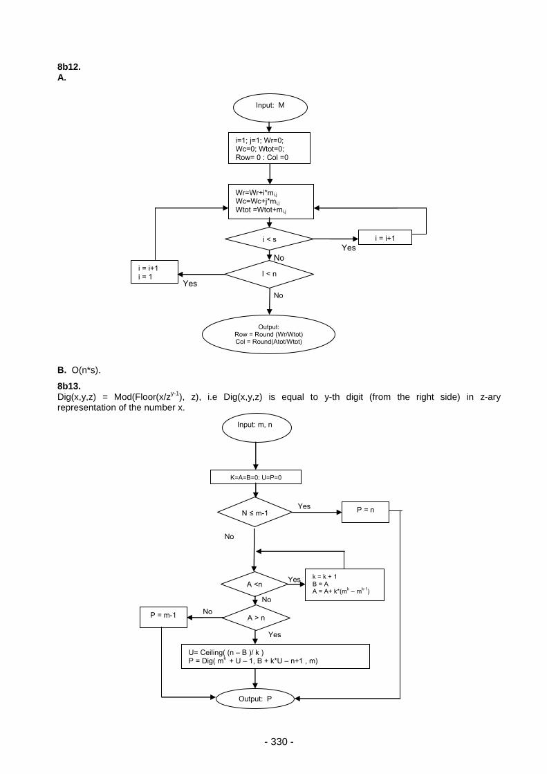
- 330 -
8b12. A.
B. O(n*s).
8b13. Dig(x,y,z) = Mod(Floor(x/z
y-1), z), i.e Dig(x,y,z) is equal to y-th digit (from the right side) in z-ary
representation of the number x.
Input: m, n
K=A=B=0; U=P=0
N ≤ m-1
A <n
A > n
Output: P
P = m-1
P = n
k = k + 1 B = A A = A+ k*(m
k – m
k-1)
U= Ceiling( (n – B )/ k ) P = Dig( m
k + U – 1, B + k*U – n+1 , m)
Yes
Yes
Yes
No
No
No
Input: M
i=1; j=1; Wr=0; Wc=0; Wtot=0; Row= 0 ; Col =0
Wr=Wr+i*mi,j Wc=Wc+j*mi,j Wtot =Wtot+mi,j
j < s
I < n
Output: Row = Round (Wr/Wtot) Col = Round(Atot/Wtot)
i = i+1 j = 1
j = j+1
Yes
No
No
Yes
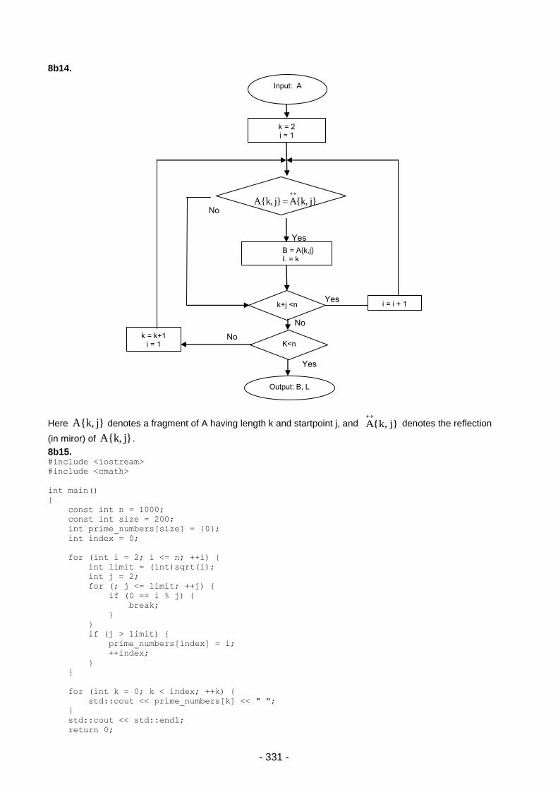
- 331 -
8b14.
Here j}A{k, denotes a fragment of A having length k and startpoint j, and j}{k,A
denotes the reflection
(in miror) of j}A{k, .
8b15. #include <iostream>
#include <cmath>
int main()
{
const int n = 1000;
const int size = 200;
int prime_numbers[size] = {0};
int index = 0;
for (int i = 2; i <= n; ++i) {
int limit = (int)sqrt(i);
int j = 2;
for (; j <= limit; ++j) {
if (0 == i % j) {
break;
}
}
if (j > limit) {
prime_numbers[index] = i;
++index;
}
}
for (int k = 0; k < index; ++k) {
std::cout << prime_numbers[k] << " ";
}
std::cout << std::endl;
return 0;
Input: A
k = 2 j = 1
j}{k,A j}A{k,
k+j <n
K<n
Output: B, L
k = k+1 j = 1
j = j + 1
B = A{k,j} L = k
Yes
Yes
Yes
No
No
No
- 332 -
}
8b16. #include <iostream>
int main(){
const int n = 1000;
const int size = 20;
int perfect_numbers[size];
int index = 0;
for (int i = 2; i <= n; ++i) {
int sum = 0;
int limit = i/2;
for (int j = 1; j <= limit; ++j) {
if (0 == i % j) {
sum += j;
}
}
if (i == sum) {
perfect_numbers[index] = i;
++index;
}
}
for (int k = 0; k < index; ++k) {
std::cout << perfect_numbers[k] << " ";
}
std::cout << std::endl;
return 0;
}
8b17. #include <iostream>
long reverse_number(long n);
int main(){
std::cout << "Please enter the number: ";
long n;
std::cin >> n;
long reverse_n = reverse_number(n);
if (n == reverse_n) {
std::cout << "Yes" << std::endl;
} else {
std::cout << "No" << std::endl;
}
return 0;
}
long reverse_number(long n){
long reverse = 0;
do {
reverse = reverse * 10 + n % 10;
n /= 10;
} while (n != 0);
return reverse;
}
8b18. #include <iostream>
// Output a partition:
void output_partition(const int n, const int *x, const int how_many_partitions){
std::cout << "Partition(" << how_many_partitions << ")" << " = ";
for (int i = 1; i <= n; i++) {
// Can't show negative numbers:
if (x[i] > 0) {
if (i == n)

- 333 -
std::cout << x[i];
else
std::cout << x[i] << " + ";
}
}
std::cout << std::endl;
}
// This is the function which generates the partitions of a given number "n".
void generate_partitions(int *x, const int n){
int k, s = 0;
int how_many_partitions = 0;
for (k = 1; k < n; k++)
x[k] = -1;
k = 1;
while (k > 0) {
// Generated a solution, let's output it then:
if (k == n) {
how_many_partitions++; // Increase the number of generated
partitions
x[n] = n - s;
output_partition(n, x, how_many_partitions);
k--;
s = s - x[k];
}
else {
// Check for another solution:
if (((n - k + 1) * (x[k] + 1)) <= n - s) {
x[k]++;
if (x[k] >= x[k - 1])
{
s = s + x[k];
k++;
}
}
else {
x[k] = -1;
k--;
s = s - x[k];
}
}
}
}
int main() {
char str[100];
int number;
std::cout << "n= " ;
while(true) {
std::cin >> str;
if (sscanf(str, "%d", &number) != 1 || number<2){
std::cout << "Please enter number >= 2!" <<std::endl;
std::cout << "n = ";
}
else{
break;
}
};
int *x = new int[number + 1];
if (x == NULL)
throw std::bad_alloc("");

- 334 -
x[0] = 0;
std::cout << "Partitions of " << number << ":\n\n";
generate_partitions(x, number);
delete [] x;
std::cin.ignore();
std::cin.get();
return 0;
}
8b19. a.
pick n,m; n_factorial = 1; m_factorial = 1; n_m_factorial = 1; for (count1= 2, n) n_factorial = n_factorial *count1; end for for (count2 = 2, m) m_factorial = m_factorial *count2; end for for (count2 = 2, n-m) m_n_factorial = m_n_factorial *count2; end for return (m_factorial * n_factorial / m_n_factorial);
b.
pick n,m; m_factorial = 1; n_m_factorial = 1; temp = 2; for (count1 = 2, m) m_factorial = m_factorial *count1; end for n_factorial = m_factorial for (count2 = m, n) m_n_factorial = m_n_factorial * temp; temp++; n_factorial = n_factorial *count2; end for return (m_factorial * n_factorial / m_n_factorial);
c.
C1(n,m) = n*m(n-m) C2(n,m) = m(n-m)
d. For the simplest algorithm (n=100, m=90), 202 multiplication and division actions will be required. For the given algorithm, 112 multiplication and division actions will be required.
8b20.
n,0i,ai m,0j,b j
mn,0k,baC
mj0ni0kji
jik
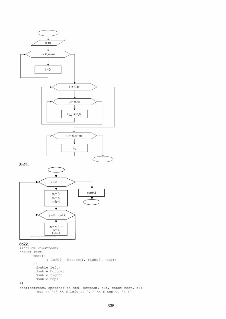
- 335 -
8b21.
8b22. #include <iostream>
struct rect{
rect()
: left(), bottom(), right(), top()
{}
double left;
double bottom;
double right;
double top;
};
std::ostream& operator <<(std::ostream& out, const rect& r){
out << "(" << r.left << ", " << r.top << ") ("
sort(c)
i = 0…n
xj = 5i
ck= xi
k=k+1
j = 0…(i-1)
yj = xi + xj
ck= xi k=k+1
- 336 -
<< r.right << ", " << r.bottom << ")";
return out;
}
std::istream& operator >>(std::istream& in, rect& r){
in >> r.left >> r.top >> r.right >> r.bottom;
return in;
}
void intersection(const rect& a, const rect& b, rect& r){
r.left = std::max(a.left, b.left);
r.bottom = std::max(a.bottom, b.bottom);
r.right = std::min(a.right, b.right);
r.top = std::min(a.top, b.top);
}
bool is_valid(const rect& r){
return (r.left <= r.right) && (r.bottom <= r.top);
}
int main(){
rect a, b;
std::cin >> a >> b;
rect r;
intersection(a, b, r);
if ( is_valid(r) ) {
std::cout << r << std::endl;
} else {
std::cout << "Has no intersection!" << std::endl;
}
return 0;
}
8b23. #include <iostream>
int main() {
unsigned long long n;
std::cin >> n;
// The number of intersection of diagonals when no 3 intersect in one
// point is equal to 4-combinations of a n, as every 4 point introduce
// a new intersection point.
unsigned long long s = n;
s = s * (n - 1) / 2;
s = s * (n - 2) / 3;
s = s * (n - 3) / 4;
std::cout << s << std::endl;
return 0;
}
8b24. #include <iostream>
#include <vector>
struct point{
point(const double& a, const double& b)
: x(a), y(b)
{}
point()
: x(0), y(0)
{}
double x;
double y;
};
typedef std::vector<point> polygon;
int sign(const double& x){
return x == 0 ? 0 : (x > 0 ? 1 : -1);
}
double cross_product(const point& a, const point& b, const point& c){
return (b.x - a.x) * (c.y - b.y) - (c.x - b.x) * (b.y - a.y);
- 337 -
}
bool is_convex(const polygon& p){
if (p.size() < 3) {
return false;
}
const size_t n = p.size();
int s = sign(cross_product(p[n - 1], p[0], p[1]));
if ( s == 0 ) {
return false;
}
for (size_t i = 0; i < n - 2; ++i) {
if ( s * cross_product(p[i], p[i + 1], p[i + 2]) <= 0 ) {
return false;
}
}
return s * cross_product(p[n - 2], p[n - 1], p[0]) > 0;
}
int main(){
size_t n;
std::cin >> n;
polygon p(n);
for ( size_t i = 0 ; i < n ; ++i ) {
std::cin >> p[i].x >> p[i].y;
}
if ( is_convex(p) ) {
std::cout << "Yes" << std::endl;
} else {
std::cout << "No" << std::endl;
}
return 0;
}
8b25. #include <iostream>
int main()
{
unsigned long long m, n;
std::cin >> m >> n;
// The number of rectangles is equal to 2-combinations of a (m + 1)
// multiplied with 2-combinations of a (n + 1).
unsigned long long s = m + 1;
s = s * m / 2;
s = s * (n + 1) * n / 2;
std::cout << s << std::endl;
return 0;
}
8b26. #include <iostream>
int main()
{
unsigned int n;
std::cin >> n;
if ( --n == 0 ) {
std::cout << 2;
} else {
unsigned long long s = 3;
while ( --n ) {
s *= 10;
}
std::cout << 8 * s;
}
return 0;
}
8b27. #include <iostream>
int main()
{
unsigned long long n;
std::cin >> n;
- 338 -
unsigned long long s = 0;
while ( (n /= 5) != 0 ) {
s += n;
}
std::cout << s;
return 0;
}
8b28. #include <iostream>
int main()
{
unsigned int n;
std::cin >> n;
unsigned long long s = 1;
unsigned long long c = 1;
while ( --n ) {
s = s* 10 + 1;
c *= 5;
}
std::cout << s * c * 15;
return 0;
}
8b29. #include <iostream>
int main()
{
unsigned int n;
std::cin >> n;
unsigned long long d = 1;
unsigned long long o = 1;
while ( --n ) {
d *= 10;
o *= 8;
}
std::cout << 9 * d - 7 * o;
return 0;
}
8b30. Schedule: tv1=1, tv2=1, tv3=1, tv4=3, tv5=3, tv6=5 Latency=5 3 Multipliers and 1 Adder 8b31. #include <iostream>
bool is_in_matrix(int** a, int n, int m, int h)
{
int i = 0;
int j = m - 1;
while (i < n && j >= 0) {
if (h == a[i][j]) {
return true;
}
if (h < a[i][j]) {
--j;
} else {
++i;
}
}
return false;
}
int main()
{
int n, m;
std::cin >> n >> m;
int** a = new int*[n];
for (int i = 0; i < n; ++i) {
a[i] = new int[m];
- 339 -
}
for (int i = 0; i < n; ++i) {
for(int j = 0; j < m; ++j) {
std::cin >> a[i][j];
}
}
int k;
std::cin >> k;
for(int i = 0; i < k; ++i) {
int h;
std::cin >> h;
std::cout << is_in_matrix(a, n, m, h) << std::endl;
}
return 0;
}
8b32. #include <iostream>
#include <cstring>
void reverse(char* s)
{
size_t l = std::strlen(s) - 1;
for (int i = 0; i <= l / 2; ++i)
{
std::swap(s[i], s[l - i]);
}
}
void rotate(char* s, size_t n)
{
size_t l = std::strlen(s);
n %= l;
if ( n == 0 ) {
return;
}
reverse(s);
reverse(s + l - n);
char t = s[l - n];
s[l - n] = '\0';
reverse(s);
s[l - n] = t;
}
int main()
{
size_t l;
size_t c;
std::cin >> l;
char* s = new char[l];
std::cin >> s;
std::cin >> c;
rotate(s, c);
std::cout << s << std::endl;
return 0;
}
8b33. #include <iostream>
#include <queue>
int main()
{
size_t N;
size_t M;
std::cin >> M;
std::cin >> N;
int n;
std::priority_queue<int> p;
for (size_t i = 0; i < M; ++i) {

- 340 -
std::cin >> n;
p.push(n);
if (p.size() > N) {
p.pop();
}
}
while (!p.empty()) {
std::cout << p.top() << " ";
p.pop();
}
return 0;
}
8b34. #include <iostream>
#include <cmath>
bool is_square(size_t k)
{
size_t p = std::sqrt(k);
return p * p == k;
}
int main()
{
size_t N, k;
std::cin >> N;
std::cin >> k;
std::cout << (is_square(k) ? "Open" : "Close") << std::endl;
return 0;
}

- 341 -
9. NANOELECTRONICS a) Test questions 9a1. E 9a2. C 9a3. E 9a4. C 9a5. E 9a6. D 9a7. B
- 342 -
b) Problems 9b1. It is possible to charge nanoparticles 1) under light illumination with photon energy, sufficient for photoelectric effect, 2) in case of the exchange of charge with a solvent that is controlled, in particular, by acidity level of pH environment. Minimum charge of nanoparticles is equal modulo charge of an electron, and the maximum actually is not limited, but in practice rarely exceeds 1-2 electron charge in an electrically neutral overall colloidal solution, as a result of dynamic equilibrium with the ions in solution. The collision of particles and, consequently, the formation of agglomerates is possible if the kinetic energy of their thermal motion exceeds the potential
energy of the Coulomb repulsion. For spherical silicon nanocrystals, having density of-Si equal to =2 g/cm3,
can compute mass 3
34 RM and estimate the minimum speed V0, at which collision is possible:
R
qMVMV
2422 0
22
0
2
0
,
where 0 – dielectric constant, – permittivity of environment.
Then for nanoparticle with R=1nm and charge q =2е (е=1.6*10-19
Kl) in benzol (=2.3) the following will be
obtained
0322
0
0
422 R
q
RM
qV 155 m/s.
Estimate the average thermal speed VT from the following relation:
kTMVT
2
3
2
2
,
where k – Boltzmann constant, Т – temperature in Kelvin degrees.
Then R
kT
RM
kTVT
4
33 40 m/s for Т=30 К, which is much smaller than the above calculated V0,
and it means a conflict of nanoparticles in benzene and their subsequent agglomeration is unlikely.
At the same time for the colloidal solution of similar nanocrystals in water ( = 80), V0 26 м/с < VT is obtained which means high probability of constants of nanoparticles and, consequently, their agglomeration. The probability of agglomeration, obviously depends on the size of nanoparticles and increases with increasing R due to a stronger dependence on the parameter values V0 . In very dilute colloidal solutions in the above 2 partial approximation, the possibility of contact of nanoparticles in a collision does not depend on the concentration of particles. However, with the growth of the latter, the probability of collisions is obviously increasing, and thus increases the probability of agglomeration. Moreover, given the dependence of the effective permittivity on the concentration of nanoparticles, with the increase of the latter the probability of collision of charged particles may change,
increasing, in particular, for silicon nanocrystals ( = 12) in benzene. In accordance with the above analysis, the possibility of collision of nanoparticles, obviously, depends on temperature and increases with increasing T, due to increased VT, which should lead to an increase in the probability of agglomeration. At the same time, in case of temperature increase the agglomerates can be destroyed by thermal motion of particles. All this leads to a nonmonotonic dependence of the probability of agglomeration of the temperature. 9b2.
1) Sectional area equals to r2. For nanoparticles of radius, this value is 3.14(5010
-9 m)
2 = 7.8510
-15 m
2.
Then, according to the written formula v = (20.720.4 H / (1170 kg/m3 10
7 7.8510
-15 m
2))
1/2 = 79.2 m/s
2) Nanocluster has ionic structure [W6I8]4+
(I-)4. Only outer-iodine can be precipitated by silver nitrate.
[W6I8]I4 + 4AgNO3 = 4AgI + [W6I8](NO3)4 Cation is octahedron of atoms of tungsten, on each edge of which iodine atom is located. 3) Any reasonable means are accepted. In particular, consider the option of breaking a compact mercury into nanoparticles with large surface area and their subsequent dispersion in the molten sulfur (this will ensure a complete course of the reaction) to form insoluble in water and most acids, mercuric sulphide, which can be used as component paints.
4) The calculation as per the given formula gives (Eg)2 = 1.46810
-37 J
2, hence Eg = 3.8310
-19 J. This
corresponds to the wavelength = hc/Eg = 6.6210-34
Js 3 108 m/s / (3.8310
-19 J) = 5.210
-7m = 520
nm, which corresponds to the green color.
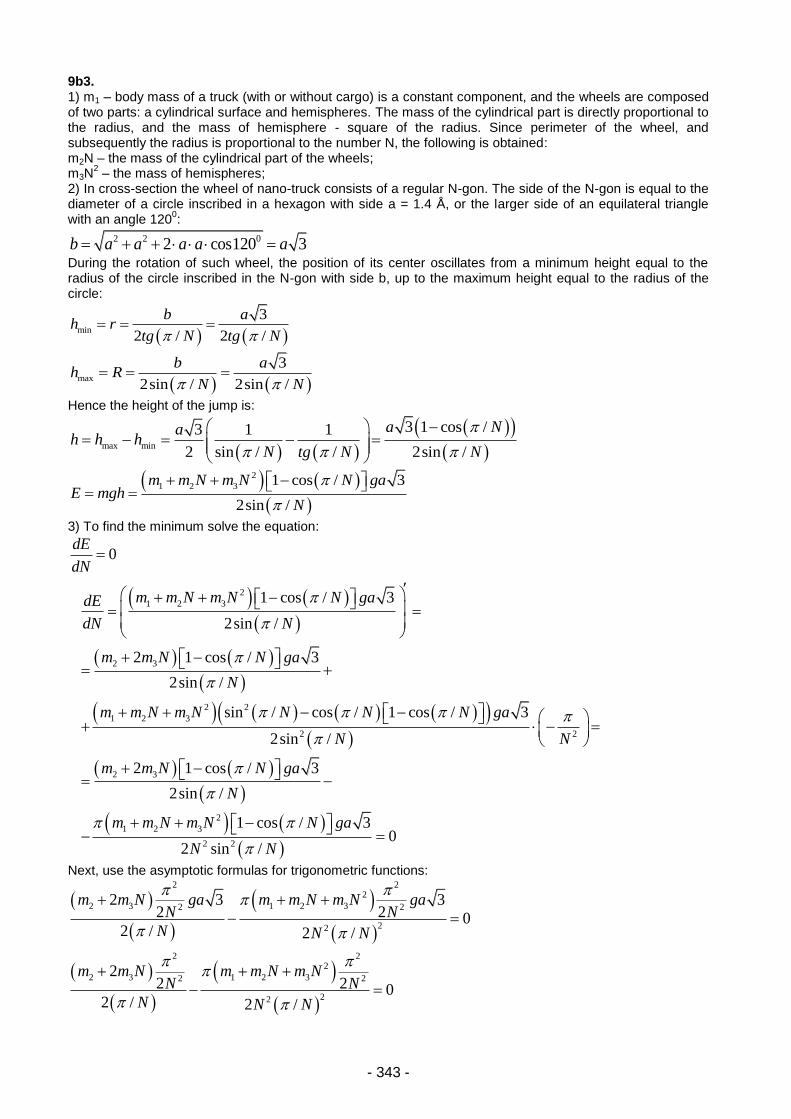
- 343 -
9b3. 1) m1 – body mass of a truck (with or without cargo) is a constant component, and the wheels are composed of two parts: a cylindrical surface and hemispheres. The mass of the cylindrical part is directly proportional to the radius, and the mass of hemisphere - square of the radius. Since perimeter of the wheel, and subsequently the radius is proportional to the number N, the following is obtained: m2N – the mass of the cylindrical part of the wheels; m3N
2 – the mass of hemispheres;
2) In cross-section the wheel of nano-truck consists of a regular N-gon. The side of the N-gon is equal to the diameter of a circle inscribed in a hexagon with side a = 1.4 Å, or the larger side of an equilateral triangle with an angle 120
0:
2 2 02 cos120 3b a a a a a
During the rotation of such wheel, the position of its center oscillates from a minimum height equal to the radius of the circle inscribed in the N-gon with side b, up to the maximum height equal to the radius of the circle:
min
3
2 / 2 /
b ah r
tg N tg N
max
3
2sin / 2sin /
b ah R
N N
Hence the height of the jump is:
max min
3 1 cos /3 1 1
2 sin / / 2sin /
a Nah h h
N tg N N
2
1 2 3 1 cos / 3
2sin /
m m N m N N gaE mgh
N
3) To find the minimum solve the equation:
0dE
dN
2
1 2 3
2 3
2 2
1 2 3
2 2
2 3
2
1 2 3
1 cos / 3
2sin /
2 1 cos / 3
2sin /
sin / cos / 1 cos / 3
2sin /
2 1 cos / 3
2sin /
1 cos / 3
2
m m N m N N gadE
dN N
m m N N ga
N
m m N m N N N N ga
N N
m m N N ga
N
m m N m N N ga
2 20
sin /N N
Next, use the asymptotic formulas for trigonometric functions:
2 22
2 3 1 2 32 2
22
2 22
2 3 1 2 32 2
22
2 3 32 2 0
2 / 2 /
22 2 0
2 / 2 /
m m N ga m m N m N gaN N
N N N
m m N m m N m NN N
N N N
- 344 -
2
1 2 32 3
2
2
2 3 1 2 3
2
2
1 3
2
20
4 4
20
0
m m N m Nm m N
N N
m m N m m N m N
N N
m m N
N
Find N:
1
3
1000020
25
mN
m
Find the energy:
J
mkg
Hkg
E 33
103
23
2
102.5)20/sin(2
3104.18.9)20/cos(1101002.6
20252070010000
9b4. 1)
2) Hole is an excited quantum state of multi-electron system, characterized by the thing that one of the single-electron states is unoccupied (from physical encyclopedia). Hole is a point from where an electron went and which can be represented as a quasiparticle with a positive charge equal to the charge of an electron. 3) The luminescence is the radiation of atoms, molecules, ions and other more complex particles, resulting from an electronic transition in these particles during their return from excited to normal state. 4) It is obvious that the addition for the crystal with 1cm radius associated with the quantum behavior would
be neglible, in this case Eg = E0 = 2.8810-19
J. The following is obtained for the crystal with 1nm radius as
per the given formula: Eg2 = 8.2910
-38 + (6.2610
-68)/ (1.0910
-31) = 8.2910
-38 + 5.7410
-37 = 6.5710
-37 J
2
(All calculations are in SI units). Hence Eg = 8.110-19
J. 5) Visible light has a range of 400-750 nm. The smaller the wavelength, the greater the energy, the smaller the radius of the nanoparticle. That is, the minimum size of the nanoparticle will be responsible of the
luminescence light with a wavelength of 400 nm, which corresponds to the energy Eg = hv = hc/ = (6.6210-
34 Js) (3 10
8 m/s) / (410
-7 m) = 4.9710
-19 J. Transforming the expression to find Eg, this is obtained: r
2 =
(E0h2) / [2 (Eg
2 – E0
2) m] = 1.2610
-85 / 3.5810
-68 = 3.5210
-18 m
2, hence r = 1.8810
-9 m or 1.88 nm.
6) Cd(C17H33COO)2 + SeP(C8H17)3 = CdSe + PO(C8H17)3 + (C17H33CO)2O 7) The atmosphere of argon is needed to prevent oxidation of raw and end products. The solvent is chosen high-boiling and inert with respect to the quantum dots. Heating during the synthesis is necessary for obtaining well-crystallized one-dimensional quantum dots. The reagents are selected so as to ensure solubility in appropriate solvents and to eliminate chemical interaction with it. Also reagents must be easy to obtain and store, and have as much molecular weight as possible. The proposed method for the second part of the question is completely unacceptable. a) The boiling temperature of water is 100 º C lower than the optimum temperature of synthesis. b) It is known that cadmium salts are considerably hydrolyzed by a cation and have acid reaction medium,
E Bulk semiconductor
Valence band
Conduction band
Band gap E0
Quantum dot
Occupied states
Unoccupied states
Eg
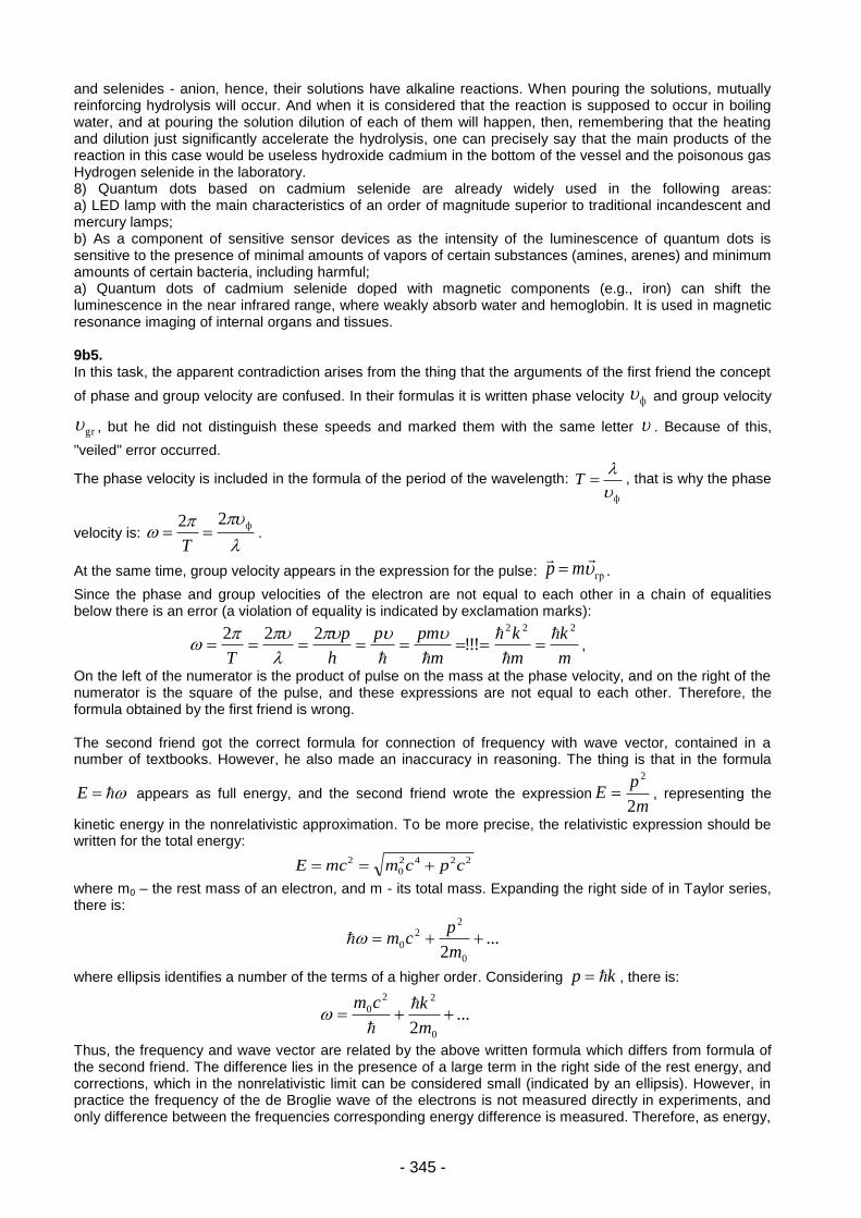
- 345 -
and selenides - anion, hence, their solutions have alkaline reactions. When pouring the solutions, mutually reinforcing hydrolysis will occur. And when it is considered that the reaction is supposed to occur in boiling water, and at pouring the solution dilution of each of them will happen, then, remembering that the heating and dilution just significantly accelerate the hydrolysis, one can precisely say that the main products of the reaction in this case would be useless hydroxide cadmium in the bottom of the vessel and the poisonous gas Hydrogen selenide in the laboratory. 8) Quantum dots based on cadmium selenide are already widely used in the following areas: a) LED lamp with the main characteristics of an order of magnitude superior to traditional incandescent and mercury lamps; b) As a component of sensitive sensor devices as the intensity of the luminescence of quantum dots is sensitive to the presence of minimal amounts of vapors of certain substances (amines, arenes) and minimum amounts of certain bacteria, including harmful; a) Quantum dots of cadmium selenide doped with magnetic components (e.g., iron) can shift the luminescence in the near infrared range, where weakly absorb water and hemoglobin. It is used in magnetic resonance imaging of internal organs and tissues. 9b5. In this task, the apparent contradiction arises from the thing that the arguments of the first friend the concept
of phase and group velocity are confused. In their formulas it is written phase velocity ф and group velocity
gr , but he did not distinguish these speeds and marked them with the same letter . Because of this,
"veiled" error occurred.
The phase velocity is included in the formula of the period of the wavelength:
ф
T , that is why the phase
velocity is:
ф22
T.
At the same time, group velocity appears in the expression for the pulse: гр
mp .
Since the phase and group velocities of the electron are not equal to each other in a chain of equalities below there is an error (a violation of equality is indicated by exclamation marks):
m
k
m
k
m
pmp
h
p
T
222
!!!222
,
On the left of the numerator is the product of pulse on the mass at the phase velocity, and on the right of the numerator is the square of the pulse, and these expressions are not equal to each other. Therefore, the formula obtained by the first friend is wrong. The second friend got the correct formula for connection of frequency with wave vector, contained in a number of textbooks. However, he also made an inaccuracy in reasoning. The thing is that in the formula
E appears as full energy, and the second friend wrote the expressionm
pE
2
2
, representing the
kinetic energy in the nonrelativistic approximation. To be more precise, the relativistic expression should be written for the total energy:
2242
0
2 cpcmmcE
where m0 – the rest mass of an electron, and m - its total mass. Expanding the right side of in Taylor series, there is:
...2 0
22
0 m
pcm
where ellipsis identifies a number of the terms of a higher order. Considering kp , there is:
...2 0
22
0 m
kcm
Thus, the frequency and wave vector are related by the above written formula which differs from formula of the second friend. The difference lies in the presence of a large term in the right side of the rest energy, and corrections, which in the nonrelativistic limit can be considered small (indicated by an ellipsis). However, in practice the frequency of the de Broglie wave of the electrons is not measured directly in experiments, and only difference between the frequencies corresponding energy difference is measured. Therefore, as energy,
- 346 -
the frequency of de Broglie waves can be measured not from the absolute zero, but from an arbitrary zero
level. This allows choosing as the origin of frequency value
2
0cm. Then the formula, obtained by the
second friend, is true for nonrelativistic approximation:
m
k
2
2
9b6. First, explain in more detail, what is the proposed "paradox". Recall what the concept of wave-particle duality is: "All microscopic objects have both wave and corpuscular properties. Their movement in space must be described by the wave theory. The corresponding wave field is distributed in space. However, when measuring the microparticle, space is registered to a certain point as a single entity with all the characteristics of the particle (mass, charge, energy, etc.). The measurement result is probabilistic in nature, to predict where the particle will be detected with certainty unit is impossible. One can only talk about the probability of an event and this probability is ultimately determined by the wave field, which describes the motion of a particle in space. Simply speaking, "measurement" is an instant photograph on which the electron (or some other particle) is recorded as one point in space, as a point particle with characteristic mass, charge and other characteristics. Therefore, it would seem, not a continuous "electron cloud" is seen on the "photographs" of microworld, but a single point or several points, the position of which is determined randomly with some probability distribution.
Why a continuous cloud is seen? The answer is quite simple: actually it is not dealt with instant photography, but with "photography with great exposure." As known, instant photographs (in the literal sense of the word) do not exist, this is only an idealization, but the real photograph always has the final extract (final imaging time). The real "dimension" in this case is the interaction of atoms with a probe microscope (the scanning probe microscopy), or with an external electron beam (transmission electron microscopy - TEM). Without going into details of the interaction of an atom with a measuring device, one can identify a general property of all the microscopes discussed in such types of tasks: typical time during which images are formed (like the ones in the figure), much larger than the characteristic atomic time, therefore such images are formed statistically as a result of the myriad interactions of atoms with a microscope. For example, in transmission electron microscopy, image is formed by multiple electron beam, which interact with atoms of the sample and then are registered by the receiver. Each electron separately carries little information and cannot form an image. The same can be said about other types of microscopy. In the AFM, image is formed by processing a large number of cantilever oscillations, but even a period of one oscillation (which already represents a very complex process) is much larger than the characteristic atomic time. Therefore, measuring the interaction potential of the cantilever with an atom is a "shot with great exposure”, and this potential is formed statistically from one of the elementary acts of the electromagnetic interaction, which, in terms of quantum field theory, is the exchange of quanta of electromagnetic field - photons. What is the characteristic atomic time, and how can it be assessed? This is the time during which phase of the wave function (wave field, as discussed above), describing the electron shell of the atom, manages to change to the order of 2π. To put it simply, this is the time during which significant changes occur in atom. If an electron is found at some point (more precisely, in a sufficiently small neighborhood), then the wave field, describing this electron is localized (concentrated) in this neighborhood. For the wave field to “blur”
- 347 -
again and take all the characteristic volume of the atom, it takes time of atomic. The atomic time is estimated by:
at
atE
t
where 341005,1 J·s – Planck's constant with feature, atE – characteristic energy of an electron in an
atom (taken modulo). The above written formula can be obtained from Heisenberg's uncertainty relation, written for the energy and time:
tE
It can also be obtained from the consideration that the phase of the wave function contains term t , where
– cyclic frequency, and therefore the phase changes by 2π in time
ET
22 .
A characteristic electron energy can be estimated as the energy of an electron in the ground state of the simplest atom - hydrogen atom. This value is called the Rydberg (denoted by Ry) and is equal to Eat = Ry = 13,6 эВ = 2,18·10
-18J. An estimate for the atomic time is obtained:
tat ≈ 5·10-17
с.
Obviously, this is an extremely short time compared to the time of imaging, given as examples in the problem. For comparison, the maximum oscillation frequency of the cantilever is of the order of several megahertz, which corresponds to the period of oscillation T ~ 10
-6 s. In scanning electron microscopy, image
is formed as a result of multiple interactions of electrons with the sample matrix and the receiver, each of which has a length greater than the atomic time. Also note that the minimum laser pulse duration is of the order of several femtoseconds, which is also much larger than the atomic time. 9b7. 1. Since gold has a high conductivity (~4,3*10
7cm) and rather thin contacts can be obtained from it (plastic
deformation at not very high temperatures). For tungsten - high conductivity (~1,2*107
Cm), developed method of obtaining thin needles for STM. 2. Physicists have observed the effect of quantum conductance. This is seen from the piecewise linear nature of the CVC. Reducing the size of the conductor leads to a decrease in the levels that determine the conductivity. Thus, not completely filled band appears below the Fermi level, but a set of subbands which are separated by "forbidden" minibands. The specific conductivity of tungsten GW = 18200000 Cm/m. Subsequently, specific resistance ρW = 1/GW = 5,4945*10
-8 Ohm*m.
Formulas for calculation: Ssec = π*r
2 = (π*d
2)/4; R = ρ*l/Ssec.
Let l=1m.
Diameter Diameter, m Sсеч, m2
R, Ohm
1 mm 1*10-3
7,85*10-7
7*10-2
1 um 1*10-6
7,85*10-13
7*104
10 nm 1*10-8
7,85*10-17
7*108
1 nm 1*10-9
7,85*10-19
7*1010
Using formula U = I*R, plot the following graph.
- 348 -
1. Plot the chart of dependence of conduction on the applied voltage as per data given in the table.
0 100 200 300 400 500 600
0
10
20
30
40
50
60
I, м
кА
U, мВ
I (U)
At least 3 regions with different angles of slope of the curve can be clearly distinguished on the presented chart. Calculate the angles for 3 regions:
From 150 to 300 mV - 0,07318 uA/mV = 7,7318*10-5
cm = G0; From 300 to 500 mV - 0,12141 uA/mV = 12,141*10
-5 cm = 1,5*G0;
From 500 to 600 mV - 0,18484 uA/mV = 18,484*10-5
cm = 2,3*G0 (for the given case it must be 2*G0, however, due to errors in the calculation of the tangent, somewhat conservative value is obtained).
1mm
1mA
10nm
1nm
100
10
1
0.1
0.01
1E-3
1E-4
1E-5
1E-6
1E-7
1E-8
1E-9
1E-10
1E-11
0 5 10 15 20
U, mkV
60
50
40
0
20
10
0
0 100 200 300 400 500 600
I, μ
A
U, mV
I (U)
U, mV
I, μ
A
- 349 -
0 100 200 300 400 500 600
0
10
20
30
40
50
60
I, м
кА
U, мВ
y = a + b*x
R^2 0,99834
Value
Intercept -21,56619
Slope 0,12141
y = a + b*x
R^2 0,99959
Value
Intercept -5,27857
Slope 0,07318
y = a + b*x
R^2 0,9968
Value
Intercept -54,62805
Slope 0,18484
Next, construct graph G (U) as per calculated data:
200 300 400 500 600
6,0x10⁻⁵
8,0x10⁻⁵
1,0x10⁻⁴
1,2x10⁻⁴
1,4x10⁻⁴
1,6x10⁻⁴
1,8x10⁻⁴
2,0x10⁻⁴
G, С
м
U, мВ
G (U)
Constant G0 is usually applied to the above described effect. What is this constant called? What is its dimension and value in the SI system? And for what is this value currently used? (3 points)
G0 = 2e2/h - quantum of conductance.
e = 1,6*10-19
Kl, h = 6,6*10-34
J*s, consequently G0 = 7,75*10-5
cm. It (or rather its inverse) is used to calibrate the resistance and since 1990 has been the benchmark
for measuring the resistance. 9b8. Answer 1: It is known that films of mesoporous silicon have great specific surface, and its limit reaches the value of about 800 m
2/g. The presence of the developed surface of porous silicon causes the presence of
her huge number of defects - dangling silicon bonds, which in turn are trapping centers for FCC. Тhe fact that in the process of electrochemical etching of crystalline silicon, dopant atoms are not "washed" with the silicon atoms must also be taken into account. Therefore, reducing the concentration of FCCs in the meso-PC cannot be attributed to the "removal" of the substance. Answer 2: Using expression for crystalline silicon it can be written:
2
)( SicSicsthz
nASicN ,
U, mV
I, μ
A
U, mV
G,
cm

- 350 -
For porous silicon:
)p(
nA)PC(N PCPC
FCC
12τλ
α,
where constemcA 22*
0
32 /4 , p = 0.6, c-Si, meso-PC – absorption coefficient for crystalline and
porous silicon, measured at a wavelength of , nc-Si = 3.4, nmeso-PC = 1.7 – refractive index for crystalline and porous silicon, respectively. Using the above written formulas to calculate the concentration of free charge carriers in mesoporous silicon, the following is obtained:
SicSic
FCCPCmesoPCmesoFCC
np
SicNnPCN
)1(
)()( ,
where Nc-Si is equal to 1020
cm-3
. Substituting numerical values, the following is obtained:
319
1
3201
106.24.3620)6.01(
107.1130)(
cm
cm
cmсмPCNFCC
Answer 3: During thermal oxidation of silicon nanocrystals, concentration in their FCCs decreases. This is due to the increasing number of defects - dangling silicon bonds that are formed during the oxidation of the samples. It is known that these dangling bonds are trapping centers for FCC. Answer 4: Microporous silicon films are obtained by electrochemical etching of lightly doped silicon substrates. The concentration of FCCs in these substrates is approximately 10
16 cm
-3. It is also known in
case of reducing the size of silicon nanocrystals to a few nanometers (as in the case of microporous silicon), the electronic spectrum of charge carriers undergoes significant changes due to quantum confinement effect. It can therefore be stated that this material is almost completely depleted of charge carriers in equilibrium. 9b9. The cantilever is represented as a rectangular beam, which bends under the effect of force F, applied along the normal to the free end of the beam. The beam theory of bending was developed by Bernoulli and Euler. It is clear that the upper surface due to deformation is accustomed, and the upper one stretches. For simplicity, beam is replaced by a segment which is bent under load and at each point the curvature is proportional to the moment of external forces. For small deflections of the curvature is almost equal to the second derivative.
So, the interval in the undisturbed position is described by ( ) , and when the load has a certain
dependence ( ), which is to be found.
Thus 𝐽
( ).
The coefficient of proportionality 𝐽 is called the flexural rigidity and is equal to the product of the modulus of
elasticity of the material of the beam on the moment of inertia.
Modulus of elasticity is given in the problem, and the moment of inertia is given by 𝐽
.
So there is a differential equation with boundary conditions:
{
𝐽
( )
( )
( )
Solution of this system:
(
) or
(
)
For there is the real height of the object: ( )
.
Generally speaking, the signal of deflection in АFМ is proportional to cantilever deflection, that is, Z’, but in solving the problem it could also be simplified and assumed that the signal is proportional to height. Both options were considered correct solutions. Estimate as per the order of the values obtained. Typical force at work on AFM has the order of F = 1 nN. According to the formula, this corresponds to
‐ ‐
‐ ‐
‐
‐
- 351 -
Let's see what happens if the beam is put in the middle of the cantilever:
(
)
That is, there was a great mistake in 60%! When calculating through derivative, the error is 25%. The difference between the answers is large, but as first of all it is important to do calculations in the first question, they are both counted as correct. Since Z' is linearly dependent on the force, the same relative error will be obtained at different forces (i.e., heights). Questions 2 and 3. The data in the topographic images are usually formed as follows. Feedback monitors changes in signal deflection and generates such a signal to move the piezoelectric ceramic to compensate the deviation of all time. Piezoceramic is calibrated and its move (exactly known in nm) gives a high-rise image. Thus, the incorrect position of the beam on the cantilever does not directly lead to a distortion of the height of objects on topographic images, but also significantly reduces signal/noise ratio. It is more critical for small objects (DNA, thin films, etc.). Questions 4. To minimize this error, a laser system must be properly set up. But if not sure, one can accurately adjust the laser by choosing a shorter and more rigid cantilever.
9b10. When hitting a hard surface, the stream breaks up into many drops of different diameters. Due to surface tension, the potential energy of the stream, that crashed on the drops, increases. To estimate, assume that for the formation of drops of a certain diameter at impact it is necessary that the kinetic energy of a selected volume of the drop in the stream be greater than the potential energy of the surface tension of the drop after its discharge from the stream. According to the law of conservation of energy:
2 2
0 0
2 2
m V m VS
where S – surface area of drops, m0 – mass of drop, V - the speed of drop after impact.
The process of drop formation of a certain diameter has a threshold as per kinetic energy (kinetic energy of a drop after impact is zero). Thus, the condition of the threshold for drop formation:
2 3 224
3R R V
6V
R
For drops with a diameter of 100 nm, the following is obtained:
692 /V m s
R
which is less than the speed of sound in air. Consequently, this stream will be heard. For drops with a diameter of 10 nm:
6290 /V m s
R
which is also slightly less than the speed of sound.
9b11. Due to quantization of electron movement, the effective bandgap increases. In conductance region, the
energy of basic state (n=1) of electron (*
00.067m m ) increases by 55.77 mEV. In valence region (
*
00.4hhm m ) on the contrary – it decreases by 9.34 mEV. The change of effective bandgap will equal
65.11mEV. Thus, for extensional GaAs, the bandgap is by 65.11mEV smaller than the “effective bandgap” of
the GaAs/AlAs quantum well of 100Å width (the energy is equal to 2 2 2
* 22n
nE
m d
).
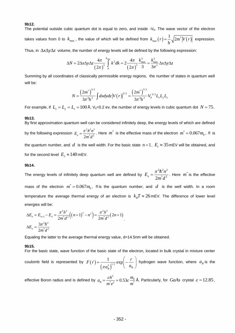
- 352 -
9b12. The potential outside cubic quantum dot is equal to zero, and inside -V0. The wave vector of the electron
takes values from 0 to maxk , the value of which will be defined from *
max
12k r m V r
h expression.
Thus, in x y z volume, the number of energy levels will be defined by the following expression:
max 3 32 max max
3 3 2
0
4 42 2
3 32 2
kk k
N x y z k dk x y z
Summing by all coordinates of classically permissible energy regions, the number of states in quantum well
will be:
3/ 2 3/ 2
* *3/ 2 3/ 2
02 2 2 2
2 2
3 3x y z
m mN dxdydz V r V L L L
h h
For example, if 100x y zL L L Å, V0=0.2 ev, the number of energy levels in cubic quantum dot 75N .
9b13. By first approximation quantum well can be considered infinitely deep, the energy levels of which are defined
by the following expression 2 2 2
* 22n
nE
m d
. Here
*m is the effective mass of the electron *
00.067m m , n is
the quantum number, and d is the well width. For the basic state 1n , 1 35E mEV will be obtained, and
for the second level 2 140E mEV.
9b14.
The energy levels of infinitely deep quantum well are defined by
2 2 2
* 22n
nE
m d
. Here
*m is the effective
mass of the electron *
00.067m m , n is the quantum number, and d is the well width. In a room
temperature the average thermal energy of an electron is 26Bk T mEV. The difference of lower level
energies will be:
2 2 2 22 2
1 * 2 * 2
2 2
* 2
1 2 12 2
3
2
n n n
n
E E E n n nm d m d
Em d
.
Equaling the latter to the average thermal energy value, d=14.5nm will be obtained.
9b15. For the basic state, wave function of the basic state of the electron, located in bulk crystal in mixture center
coulomb field is represented by
1/ 23
1exp
BB
rF r
aa
hydrogen wave function, where Ba is the
effective Boron radius and is defined by 2
0
* 2 *0.53B
ma
m e m
Å. Particularly, for GaAs crystal 12.85 ,
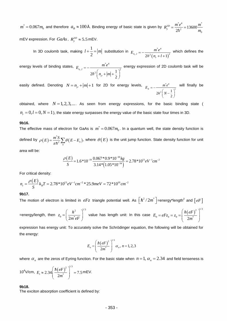
- 353 -
*
00.067m m and therefore 100Ba Å. Binding energy of basic state is given by * 4 *
3
2
0
136002
D
y
m e mR
m
mEV expression. For GaAs , 3 5.5D
yR mEV.
In 3D coulomb task, making 1
2l m substitution in
* 4
, 222 1rn l
r
m eE
n l
which defines the
energy levels of binding states, * 4
, 2
2 12
2
rn l
m eE
n m
energy expression of 2D coulomb task will be
easily defined. Denoting 1N n m for 2D for energy levels, * 4
2
2 12
2
N
m eE
N
will finally be
obtained, where 1,2,3,...N . As seen from energy expressions, for the basic binding state (
0, 0, 1rn l N ), the state energy surpasses the energy value of the basic state four times in 3D.
9b16.
The effective mass of electron for GaAs is *
00.067m m . In a quantum well, the state density function is
defined by *
2 n
n
m SE E E
, where E is the unit jump function. State density function for unit
area will be:
3019 13 1 2
34
0.067*0.9*101.6*10 2.78*10
3.14* 1.05*10
E kgeV cm
S
For critical density:
13 1 2 10 22.78*10 *25.9 72*10c B
En k T eV cm meV cm
S
9b17.
The motion of electron is limited in eFz triangle potential well. As 2 */ 2m =energy*length
2 and eF
=energy/length, then
1/32
0 *2z
m eF
value has length unit: In this case
1/32
0 0 0 *2
eFE eFz z
m
expression has energy unit: To accurately solve the Schrödinger equation, the following will be obtained for
the energy:
1/3
2
*, 1,2,3
2n n
eFE n
m
where n are the zeros of Eyring function. For the basic state when 1, 2.34nn and field tenseness is
104V/cm,
1/3
2
1 *2.34 7.5
2
eFE
m
mEV.
9b18. The exciton absorption coefficient is defined by:
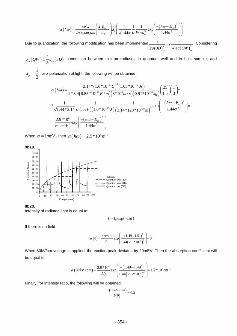
- 354 -
2 22
3 2
0 0 0
2 1 1 1exp
2 1.441.44
cv ex
p
r ex
p Eea
n cm m W a
Due to quantization, the following modification has been implemented
3 3
1 1
3ex ex
a D W a QW . Considering
2
33
ex exa QW a D connection between exciton radiuses in quantum well and in bulk sample, and
1
2pa for x polarization of light, the following will be obtained:
219 34
12 8 30
2
3 219 10
26
2
3.14* 1.6*10 1.05*10 25 1*
1.5 32*3.4 8.85*10 / 3*10 / 0.91*10
1 1 1* exp
1.441.6*101.44*3.14 3.14*120*10
2.9*10exp
1.44
ex
ex
C Js
F m m s kg
E
meV J m
E
meV
When 1meV , then 6 12.9*10 m .
9b19.
9b20. Intensity of radiated light is equal to:
0 expI I d
If there is no field:
24
23
1.49 1.512.9*100 exp 0
2.5 1.44 2.5*10
When 80kV/cm voltage is applied, the exciton peak deviates by 20mEV. Then the absorption coefficient will
be equal to:
244 1
23
1.49 1.492.9*1080 / exp 1.2*10
2.5 1.44 2.5*10kV cm cm
Finally, for intensity ratio, the following will be obtained:
80 /0.3
0
I kV cm
I
1E+20
3E+20
6E+20
9E+20
Bulk (3D) Quantum well (2D)
Quantum wire (1D)
Quantum dot (0D)
Energy (meV)
De
nsity o
f S
tate
s
2E+20
4E+20
5E+20
7E+20
8E+20
1E+21
0 0 10 20 30 40 50 60 70 80 90 100
- 355 -
I-VII ANNUAL INTERNATIONAL MICROELECTRONICS OLYMPIADS OF ARMENIA
Authors: MELIKYAN Vazgen MOVSISYAN Vilyam SIMONYAN Sargis VARDANYAN Ruben BUNIATYAN Vahe KHUDAVERDYAN Surik PETROSYAN Stepan BABAYAN Armenak HARUTYUNYAN Ashot TRAVAJYAN Misak YEGHIAZARYAN Vladimir GOMTSYAN Hovhannes MURADYAN Movses AYVAZYAN Gagik VARDANYAN Valeri MELKONYAN Slavik MINASYAN Arthur TUMANYAN Anna HAHANOV Vladimir UMNYASHKIN Sergey PETKOVIC Predrag AL-NASHASH Hasan MÜLLER-GRITSCHNEDER Daniel STEPANYAN Harutyun TANANYAN Hovhannes
GHAZARYAN Eduard KRUPKINA Tatyana MAJZOUB Sohaib ALBASHA Lutfi ASSI Ali ALOUL Fadi MAHMOODI Hamid MHAIDAT Khaldoon NELYAEV Vladislav SRINIVAS Mandalika
Translated by: GOROYAN Ruzanna
Order 999 Print run 60
Printed in the Publishing House of State Engineering University of Armenia
Yerevan, Teryan 105