Embed Size (px)
Citation preview
VBUS
PMID
OTG
D+
D–
STAT
SDA
SCL
INT
CE
SW
BTST
REGN
PGND
SYS
BAT
ILIM
TS
+3.3V
Host
REGN
SYS
USB
5V USB
bq24295
Phone
Tablet
BATTERY
C5
10 Fm
C1
C2
1 FmC3
47nF
C4
4.7 Fm
L1
2.2 Hm
SYS
SDP/DCP
Thermal Pad
R1 317W (1.5A max)
RTH
10kW
RT1
5.25kW
RT2
31.23kW
R2
2.2kW
R3
10kW
R4
10kW
R5
10kW
R6
10kW
C6
10 Fm
C7
10 Fm
20 F minm
QON Optional
Charge Enable (0°C - 45°C)
Product
Folder
Order
Now
Technical
Documents
Tools &
Software
Support &Community
An IMPORTANT NOTICE at the end of this data sheet addresses availability, warranty, changes, use in safety-critical applications,intellectual property matters and other important disclaimers. PRODUCTION DATA.
bq24295SLUSBC1B –SEPTEMBER 2013–REVISED DECEMBER 2016
bq24295 I2C Controlled 3A Single Cell USB Charger With Narrow VDC4.5-5.5V Adjustable Voltage at 1.5A Synchronous Boost Operation
1 Features
1
1
• 90% High Efficiency Switch Mode 3-A Charger• 3.9-V to 6.2-V Single Input USB-Compliant
Charger with 6.4-V Over-Voltage Protection– USB Host or Charging Port D+/D- Detection
Compatible to USB Battery Charger Spec(BC1.2)
– Support Non-Standard 2-A/1-A AdaptersDetection
– Input Voltage and Current Limit SupportsUSB2.0 and USB 3.0
– Input Current Limit: 100 mA, 150 mA, 500 mA,900 mA, 1 A, 1.5 A, 2 A, and 3 A
• Synchronous Boost Converter in Battery BoostMode with– Adjustable Output 4.55 V – 5.5 V at 1.5 A– 90% 5.1-V Boost Mode Efficiency– Fast OTG Startup (22 ms Typ)
• Narrow VDC (NVDC) Power Path Management– Instant System On with No Battery or Deeply
Discharged Battery– Ideal Diode Operation in Battery Supplement
Mode• 1.5-MHz Switching Frequency for Low Profile 1.2-
mm Inductor• I2C Port for Optimal System Performance and
Status Reporting• Autonomous Battery Charging with or without
Host Management– Battery Charge Enable– Battery Charge Preconditioning– Charge Termination and Recharge
• High Accuracy– ±0.5% Charge Voltage Regulation– ±7% Charge Current Regulation– ±7.5% Input Current Regulation– ±3% Output Voltage Regulation in Boost Mode
• High Integration– Power Path Management– Synchronous Switching MOSFETs– Integrated Current Sensing– Bootstrap Diode– Internal Loop Compensation
• Safety– Battery Temperature Sensing for Charging and
Discharging in Boost Mode– Battery Charging Safety Timer– Thermal Regulation and Thermal Shutdown– Input and System Over-Voltage Protection– MOSFET Over-Current Protection
• Charge Status Outputs for LED or Host Processor• Maximum Power Tracking Capability by Input
Voltage Regulation• 20-µA Low Battery Leakage Current and Support
Shipping Mode• 4mm x 4mm VQFN-24 Package
2 Applications• Power Bank for Smartphone, Tablet• Portable Media Players• Internet Devices
3 DescriptionThe bq24295 is a highly-integrated switch-modebattery charge management and system power pathmanagement devices for 1 cell Li-Ion and Li-polymerbattery in a wide range of power bank, tablet andother portable device applications.
Device Information(1)
PART NUMBER PACKAGE BODY SIZE (NOM)bq24295 VQFN (24) 4.00 mm x 4.00 mm
(1) For all available packages, see the orderable addendum atthe end of the datasheet.
bq24295 with USB D+/D- Detection for Chargingand Discharging in Boost Mode
2
bq24295SLUSBC1B –SEPTEMBER 2013–REVISED DECEMBER 2016 www.ti.com
Product Folder Links: bq24295
Submit Documentation Feedback Copyright © 2013–2016, Texas Instruments Incorporated
Table of Contents1 Features .................................................................. 12 Applications ........................................................... 13 Description ............................................................. 14 Revision History..................................................... 25 Description (Continued) ........................................ 46 Pin Configuration and Functions ......................... 57 Specifications......................................................... 6
7.1 Absolute Maximum Ratings ...................................... 67.2 ESD Ratings ............................................................ 67.3 Recommended Operating Conditions....................... 77.4 Thermal Information .................................................. 77.5 Electrical Characteristics........................................... 77.6 Timing Requirements .............................................. 117.7 Typical Characteristics ............................................ 11
8 Detailed Description ............................................ 148.1 Overview ................................................................. 148.2 Functional Block Diagram ....................................... 158.3 Feature Description................................................. 16
8.4 Device Functional Modes........................................ 278.5 Programming........................................................... 288.6 Register Map........................................................... 32
9 Application and Implementation ........................ 399.1 Application Information............................................ 399.2 Typical Application .................................................. 39
10 Power Supply Recommendations ..................... 4311 Layout................................................................... 43
11.1 Layout Guidelines ................................................. 4311.2 Layout Example .................................................... 44
12 Device and Documentation Support ................. 4512.1 Documentation Support ....................................... 4512.2 Receiving Notification of Documentation Updates 4512.3 Community Resources.......................................... 4512.4 Trademarks ........................................................... 4512.5 Electrostatic Discharge Caution............................ 4512.6 Glossary ................................................................ 45
13 Mechanical, Packaging, and OrderableInformation ........................................................... 45
4 Revision History
Changes from Revision A (January 2015) to Revision B Page
• Changed 58 to 0x58 in Input Source Control Register REG00 [reset = 01011000, or 0x58] heading .................................. 2• Changed 00011011 to 00111011 and 0x1B to 0x3B in Power-On Configuration Register REG01 [reset = 00111011,
or 0x3B] heading .................................................................................................................................................................... 2• Changed 4B to 0x4B in Misc Operation Control Register REG07 [reset = 01001011, or 0x4B] heading ............................ 2• Deleted last two sentences in Power-On-Reset (POR) ....................................................................................................... 16• Changed VREF to VREGN in Figure 18 ................................................................................................................................. 24• Changed 20°C to –20°C and VREF to VREGN in Figure 19 ................................................................................................. 24• Changed Equation 1 ............................................................................................................................................................ 25• Changed 58 to 0x58 in Input Source Control Register REG00 [reset = 01011000, or 0x58] heading ................................ 32• Changed 00011011 to 00111011 and 0x1B to 0x3B in Power-On Configuration Register REG01 [reset = 00111011,
or 0x3B] heading .................................................................................................................................................................. 33• Changed Bit 6 RESET from 1 to 0 in Table 9 ..................................................................................................................... 34• Changed Bit 3 RESET from 1 to 0 in Table 11 ................................................................................................................... 35• Changed Bit 2 RESET from 1 to 0 in Table 11 ................................................................................................................... 35• Changed 4B to 0x4B in Misc Operation Control Register REG07 [reset = 01001011, or 0x4B] heading .......................... 37• Changed D+/D– to input source in Table 14 ....................................................................................................................... 37• Changed last paragraph in Output Capacitor section .......................................................................................................... 40
Changes from Original (September 2013) to Revision A Page
• Added ESD Ratings table, Feature Description section, Device Functional Modes, Application and Implementationsection, Power Supply Recommendations section, Layout section, Device and Documentation Support section, andMechanical, Packaging, and Orderable Information section. ................................................................................................. 1
• Changed 5.52kΩ to 5.25kΩ in bq24295 with USB D+/D- Detection for Charging and Discharging in Boost Mode ............. 1• Changed Power Pad to Thermal Pad throughout data sheet ................................................................................................ 1• Changed REG01[5] to REG01[5] = 1 in OTG description...................................................................................................... 5
3
bq24295www.ti.com SLUSBC1B –SEPTEMBER 2013–REVISED DECEMBER 2016
Product Folder Links: bq24295
Submit Documentation FeedbackCopyright © 2013–2016, Texas Instruments Incorporated
• Added (10k NTC thermistor only) to QON description ........................................................................................................... 5• Changed ICHG = 1792 mA in IICHG_REG_ACC test conditions ...................................................................................................... 8• Changed falling to rising and TYP to 47.2% in VHTF in Electrical Characteristics .................................................................. 9• Added VIH_OTG to Electrical Characteristics .......................................................................................................................... 10• Deleted wavefroms from Typical Characteristics and added to Application Performance Plots.......................................... 11• Changed Table 3 ................................................................................................................................................................. 19• Added paragraph after Table 3............................................................................................................................................. 19• Changed Figure 15 .............................................................................................................................................................. 21• Changed from 2048 mA to 1024 mA in Table 5................................................................................................................... 22• Changed RT1 = 5.25 kΩ ..................................................................................................................................................... 25• Deleted and LSFET from Voltage and Current Monitoring in Buck Mode description ......................................................... 27• Changed REG09[5] to REG09[3] in Battery Over-Voltage Protection (BATOVP) section ................................................... 27• Changed reset = 01100000, or 60 to reset = 00100000, or 0x20 for REG02...................................................................... 34• Changed Default: 2048 mA (011000) to Default: 1024mA (001000) for bits [7:2] in REG02 .............................................. 34• Changed reset = 10011010, or 0x9A to reset = 10011100, or 0x9C for REG05 ................................................................. 35• Changed 0 to 1 for REG05 Bit 2 Reset ............................................................................................................................... 35• Changed 1 to 0 for REG05 Bit 1 Reset ................................................................................................................................ 35• Changed REG09 Bit 3 description 1 – Battery OVP ........................................................................................................... 38• Changed paragraph in Application Information ................................................................................................................... 39• Changed 5.52kΩ to 5.25kΩ in Figure 40 ............................................................................................................................. 39
4
bq24295SLUSBC1B –SEPTEMBER 2013–REVISED DECEMBER 2016 www.ti.com
Product Folder Links: bq24295
Submit Documentation Feedback Copyright © 2013–2016, Texas Instruments Incorporated
5 Description (Continued)Its low impedance power path optimizes switch-mode operation efficiency, reduces battery charging time andextends battery life during discharging phase. The I2C serial interface with charging and system settings makesthe device a truly flexible solution.
The device supports 3.9V – 6.2V USB input sources, including standard USB host port and USB charging portwith 6.4V over-voltage protection. The bq24295 is compliant with USB 2.0 and USB 3.0 power specifications withinput current and voltage regulation. To set the default input current limit, the bq24295 detects the input sourcethrough D+/D- detection following the USB battery charging spec 1.2. In addition, the bq24295 detects non-standard 2A/1A adapters. The bq24295 supports battery boost operation by supplying adjustable voltage 4.55 –5.5V (default 5.1V) on PMID pin with minimum current of 1.5A.
The power path management regulates the system slightly above battery voltage but does not drop below 3.5Vminimum system voltage (programmable). With this feature, the system maintains operation even when thebattery is completely depleted or removed. When the input current limit or voltage limit is reached, the powerpath management automatically reduces the charge current to zero. As the system load continues to increase,the power path discharges the battery until the system power requirement is met. This supplement modeoperation prevents overloading the input source.
The devices initiate and complete a charging cycle without software control. It automatically detects the batteryvoltage and charges the battery in three phases: pre-conditioning, constant current and constant voltage. At theend of the charging cycle, the charger automatically terminates when the charge current is below a preset limit inthe constant voltage phase. When the full battery falls below the recharge threshold, the charger willautomatically start another charging cycle.
The devices provide various safety features for battery charging and system operation, including negativethermistor monitoring, charging safety timer and over-voltage/over-current protections. The thermal regulationreduces charge current when the junction temperature exceeds 120°C (programmable).
The STAT output reports the charging status and any fault conditions. The INT immediately notifies the hostwhen a fault occurs.
The bq24295 is available in a 24-pin, 4x4 mm2 thin VQFN package.
STAT
SCL
SDA
VB
US
PM
ID
RE
GN
PGND
PGND
SYS
SYSO
TG
INT
4
5
6
7 8 9
15
16
17
18
222324
1
2
3
BAT
BAT13
14
BT
ST
SW
SW
192021
10 11 12
VBUS
D+
D–
ILIM TS
QO
N
bq24295
CE
5
bq24295www.ti.com SLUSBC1B –SEPTEMBER 2013–REVISED DECEMBER 2016
Product Folder Links: bq24295
Submit Documentation FeedbackCopyright © 2013–2016, Texas Instruments Incorporated
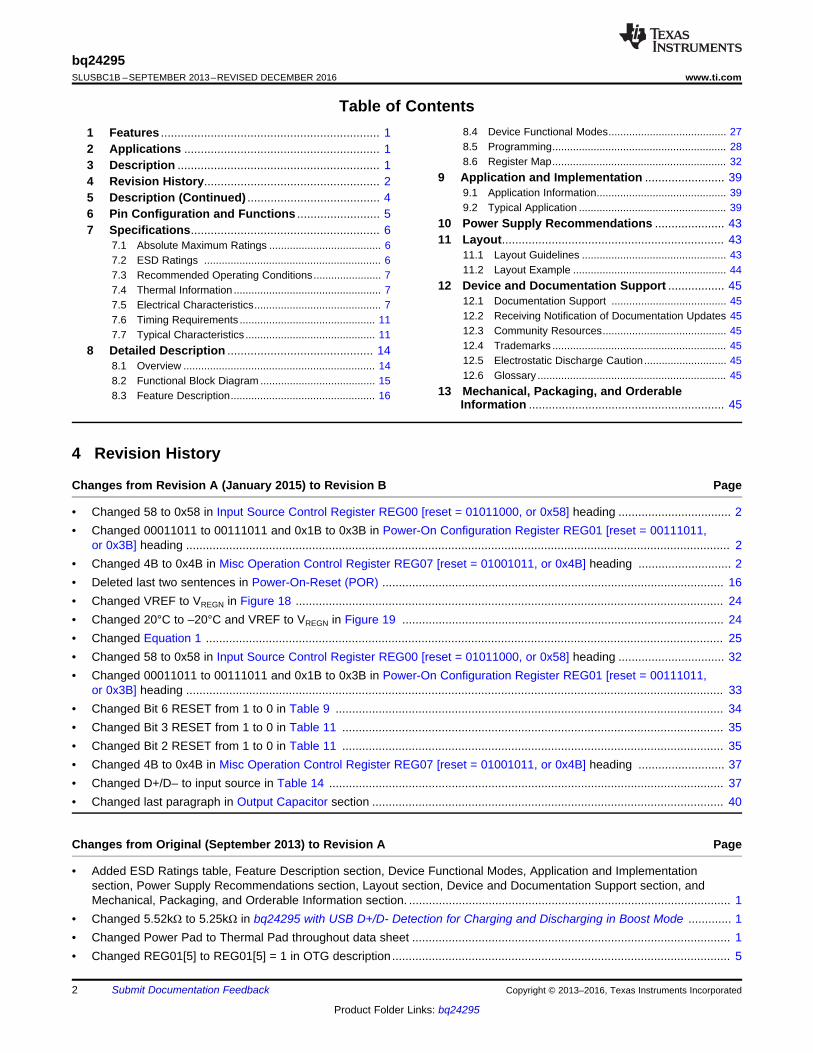
6 Pin Configuration and Functions
RGE Package24-Pin VQFN With Exposed Thermal Pad
(Top View)
Pin FunctionsPIN
TYPE DESCRIPTIONNAME NUMBER
VBUS 1,24 P Charger Input Voltage. The internal n-channel reverse block MOSFET (RBFET) is connected between VBUS andPMID with VBUS on source. Place a 1-µF ceramic capacitor from VBUS to PGND and place it as close as possibleto IC.
D+ 2 IAnalog
Positive line of the USB data line pair. D+/D– based USB host/charging port detection. The detection includes datacontact detection (DCD) and primary detection in bc1.2.
D– 3 IAnalog
Negative line of the USB data line pair. D+/D– based USB host/charging port detection. The detection includes datacontact detection (DCD) and primary detection in bc1.2.
STAT 4 O Open drain charge status output to indicate various charger operation. Connect to the pull up rail via 10-kΩ resistor.LOW indicates charge in progress. HIGH indicates charge complete or charge disabled. When any fault conditionoccurs, STAT pin in the charge blinks at 1 Hz.
SCL 5 I I2C Interface clock. Connect SCL to the logic rail through a 10-kΩ resistor.
SDA 6 I/O I2C Interface data. Connect SDA to the logic rail through a 10-kΩ resistor.
INT 7 O Open-drain Interrupt Output. Connect the INT to a logic rail via 10kΩ resistor. The INT pin sends active low, 256-µspulse to host to report charger device status and fault.
OTG 8 IDigital
OTG Enable pin. The boost mode is activated when the OTG pin is High, REG01[5] = 1, and no Input source isdetected at VBUS.
CE 9 I Active low Charge Enable pin. Battery charging is enabled when REG01[5:4] = 01 and CE pin = Low. CE pin mustbe pulled high or low.
ILIM 10 I ILIM pin sets the maximum input current limit by regulating the ILIM voltage at 1 V. A resistor is connected fromILIM pin to ground to set the maximum limit as IINMAX = (1V/RILIM) × KILIM. The actual input current limit is the lowerone set by ILIM and by I2C REG00[2:0]. The minimum input current programmed on ILIM pin is 500 mA.
TS 11 IAnalog
Temperature qualification voltage input. Connect a negative temperature coefficient thermistor. Programtemperature window with a resistor divider from REGN to TS to GND. Charge suspends or Boost disable when TSpin is out of range. A 103AT-2 thermistor is recommended.
QON 12 I BATFET enable control in shipping mode. A logic low to high transition on this pin with minimum 2ms high levelturns on BATFET to exit shipping mode. It has internal 1MΩ (Typ) pull down. For backward compatibility, whenBATFET enable control function is not used, the pin can be a no connect or tied to TS pin (10k NTC thermistoronly). (Refer to Shipping Mode for detail description).
BAT 13,14 P Battery connection point to the positive pin of the battery pack. The internal BATFET is connected between BATand SYS. Connect a 10 µF closely to the BAT pin.
6
bq24295SLUSBC1B –SEPTEMBER 2013–REVISED DECEMBER 2016 www.ti.com
Product Folder Links: bq24295
Submit Documentation Feedback Copyright © 2013–2016, Texas Instruments Incorporated
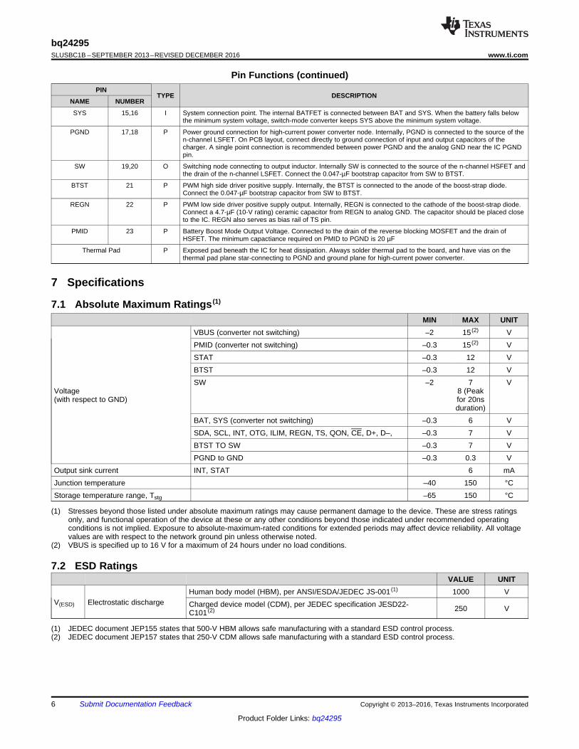
Pin Functions (continued)PIN
TYPE DESCRIPTIONNAME NUMBER
SYS 15,16 I System connection point. The internal BATFET is connected between BAT and SYS. When the battery falls belowthe minimum system voltage, switch-mode converter keeps SYS above the minimum system voltage.
PGND 17,18 P Power ground connection for high-current power converter node. Internally, PGND is connected to the source of then-channel LSFET. On PCB layout, connect directly to ground connection of input and output capacitors of thecharger. A single point connection is recommended between power PGND and the analog GND near the IC PGNDpin.
SW 19,20 O Switching node connecting to output inductor. Internally SW is connected to the source of the n-channel HSFET andthe drain of the n-channel LSFET. Connect the 0.047-µF bootstrap capacitor from SW to BTST.
BTST 21 P PWM high side driver positive supply. Internally, the BTST is connected to the anode of the boost-strap diode.Connect the 0.047-µF bootstrap capacitor from SW to BTST.
REGN 22 P PWM low side driver positive supply output. Internally, REGN is connected to the cathode of the boost-strap diode.Connect a 4.7-µF (10-V rating) ceramic capacitor from REGN to analog GND. The capacitor should be placed closeto the IC. REGN also serves as bias rail of TS pin.
PMID 23 P Battery Boost Mode Output Voltage. Connected to the drain of the reverse blocking MOSFET and the drain ofHSFET. The minimum capactiance required on PMID to PGND is 20 µF
Thermal Pad P Exposed pad beneath the IC for heat dissipation. Always solder thermal pad to the board, and have vias on thethermal pad plane star-connecting to PGND and ground plane for high-current power converter.
(1) Stresses beyond those listed under absolute maximum ratings may cause permanent damage to the device. These are stress ratingsonly, and functional operation of the device at these or any other conditions beyond those indicated under recommended operatingconditions is not implied. Exposure to absolute-maximum-rated conditions for extended periods may affect device reliability. All voltagevalues are with respect to the network ground pin unless otherwise noted.
(2) VBUS is specified up to 16 V for a maximum of 24 hours under no load conditions.
7 Specifications
7.1 Absolute Maximum Ratings (1)
MIN MAX UNIT
Voltage(with respect to GND)
VBUS (converter not switching) –2 15 (2) VPMID (converter not switching) –0.3 15 (2) VSTAT –0.3 12 VBTST –0.3 12 VSW –2 7
8 (Peakfor 20nsduration)
V
BAT, SYS (converter not switching) –0.3 6 VSDA, SCL, INT, OTG, ILIM, REGN, TS, QON, CE, D+, D–, –0.3 7 VBTST TO SW –0.3 7 VPGND to GND –0.3 0.3 V
Output sink current INT, STAT 6 mAJunction temperature –40 150 °CStorage temperature range, Tstg –65 150 °C
(1) JEDEC document JEP155 states that 500-V HBM allows safe manufacturing with a standard ESD control process.(2) JEDEC document JEP157 states that 250-V CDM allows safe manufacturing with a standard ESD control process.
7.2 ESD RatingsVALUE UNIT
V(ESD) Electrostatic dischargeHuman body model (HBM), per ANSI/ESDA/JEDEC JS-001 (1) 1000 VCharged device model (CDM), per JEDEC specification JESD22-C101 (2) 250 V
7
bq24295www.ti.com SLUSBC1B –SEPTEMBER 2013–REVISED DECEMBER 2016
Product Folder Links: bq24295
Submit Documentation FeedbackCopyright © 2013–2016, Texas Instruments Incorporated
(1) The inherent switching noise voltage spikes should not exceed the absolute maximum rating on either the BTST or SW pins. A tightlayout minimizes switching noise.
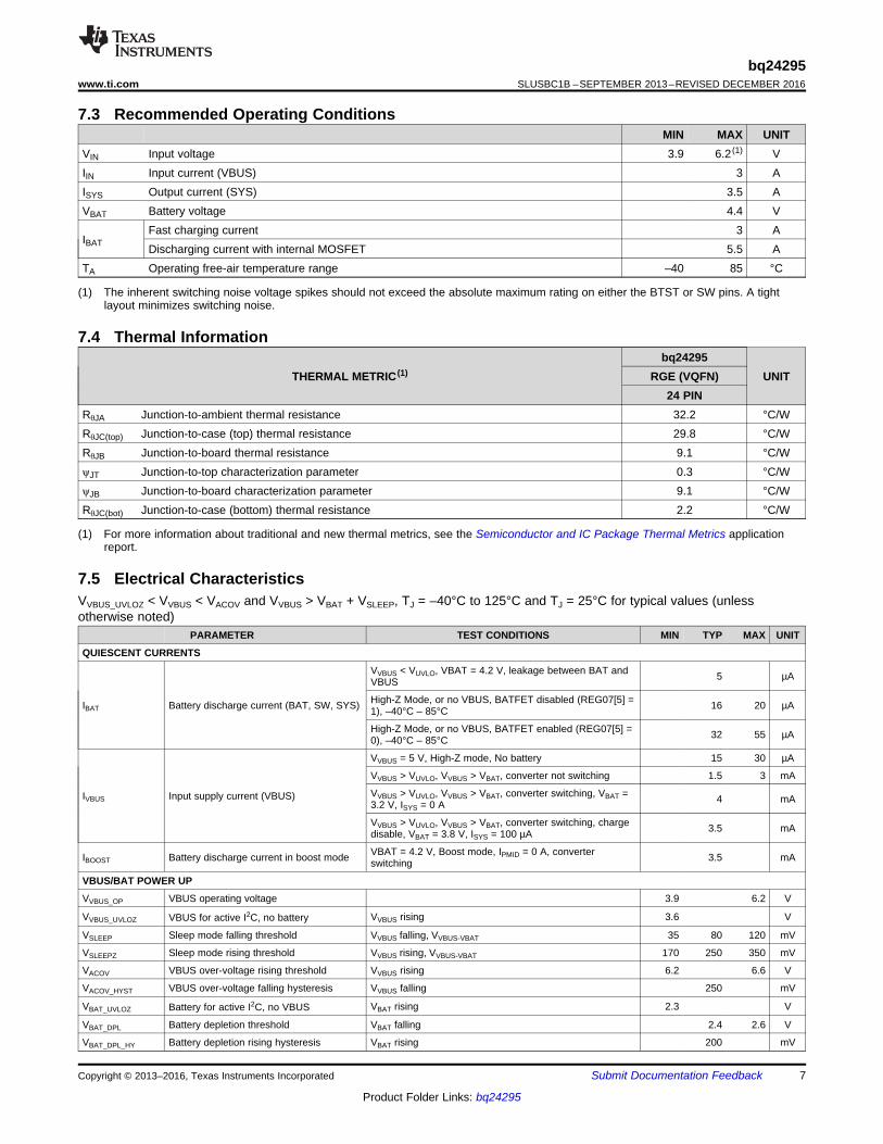
7.3 Recommended Operating ConditionsMIN MAX UNIT
VIN Input voltage 3.9 6.2 (1) VIIN Input current (VBUS) 3 AISYS Output current (SYS) 3.5 AVBAT Battery voltage 4.4 V
IBATFast charging current 3 ADischarging current with internal MOSFET 5.5 A
TA Operating free-air temperature range –40 85 °C
(1) For more information about traditional and new thermal metrics, see the Semiconductor and IC Package Thermal Metrics applicationreport.
7.4 Thermal Information
THERMAL METRIC (1)bq24295
UNITRGE (VQFN)24 PIN
RθJA Junction-to-ambient thermal resistance 32.2 °C/WRθJC(top) Junction-to-case (top) thermal resistance 29.8 °C/WRθJB Junction-to-board thermal resistance 9.1 °C/WψJT Junction-to-top characterization parameter 0.3 °C/WψJB Junction-to-board characterization parameter 9.1 °C/WRθJC(bot) Junction-to-case (bottom) thermal resistance 2.2 °C/W
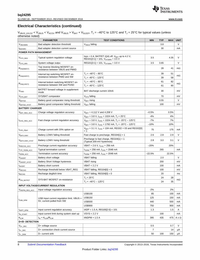
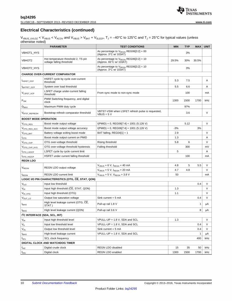
7.5 Electrical CharacteristicsVVBUS_UVLOZ < VVBUS < VACOV and VVBUS > VBAT + VSLEEP, TJ = –40°C to 125°C and TJ = 25°C for typical values (unlessotherwise noted)
PARAMETER TEST CONDITIONS MIN TYP MAX UNIT
QUIESCENT CURRENTS
IBAT Battery discharge current (BAT, SW, SYS)
VVBUS < VUVLO, VBAT = 4.2 V, leakage between BAT andVBUS 5 µA
High-Z Mode, or no VBUS, BATFET disabled (REG07[5] =1), –40°C – 85°C 16 20 µA
High-Z Mode, or no VBUS, BATFET enabled (REG07[5] =0), –40°C – 85°C 32 55 µA
IVBUS Input supply current (VBUS)
VVBUS = 5 V, High-Z mode, No battery 15 30 µA
VVBUS > VUVLO, VVBUS > VBAT, converter not switching 1.5 3 mA
VVBUS > VUVLO, VVBUS > VBAT, converter switching, VBAT =3.2 V, ISYS = 0 A 4 mA
VVBUS > VUVLO, VVBUS > VBAT, converter switching, chargedisable, VBAT = 3.8 V, ISYS = 100 µA 3.5 mA
IBOOST Battery discharge current in boost mode VBAT = 4.2 V, Boost mode, IPMID = 0 A, converterswitching 3.5 mA
VBUS/BAT POWER UP
VVBUS_OP VBUS operating voltage 3.9 6.2 V
VVBUS_UVLOZ VBUS for active I2C, no battery VVBUS rising 3.6 V
VSLEEP Sleep mode falling threshold VVBUS falling, VVBUS-VBAT 35 80 120 mV
VSLEEPZ Sleep mode rising threshold VVBUS rising, VVBUS-VBAT 170 250 350 mV
VACOV VBUS over-voltage rising threshold VVBUS rising 6.2 6.6 V
VACOV_HYST VBUS over-voltage falling hysteresis VVBUS falling 250 mV
VBAT_UVLOZ Battery for active I2C, no VBUS VBAT rising 2.3 V
VBAT_DPL Battery depletion threshold VBAT falling 2.4 2.6 V
VBAT_DPL_HY Battery depletion rising hysteresis VBAT rising 200 mV
8
bq24295SLUSBC1B –SEPTEMBER 2013–REVISED DECEMBER 2016 www.ti.com
Product Folder Links: bq24295
Submit Documentation Feedback Copyright © 2013–2016, Texas Instruments Incorporated
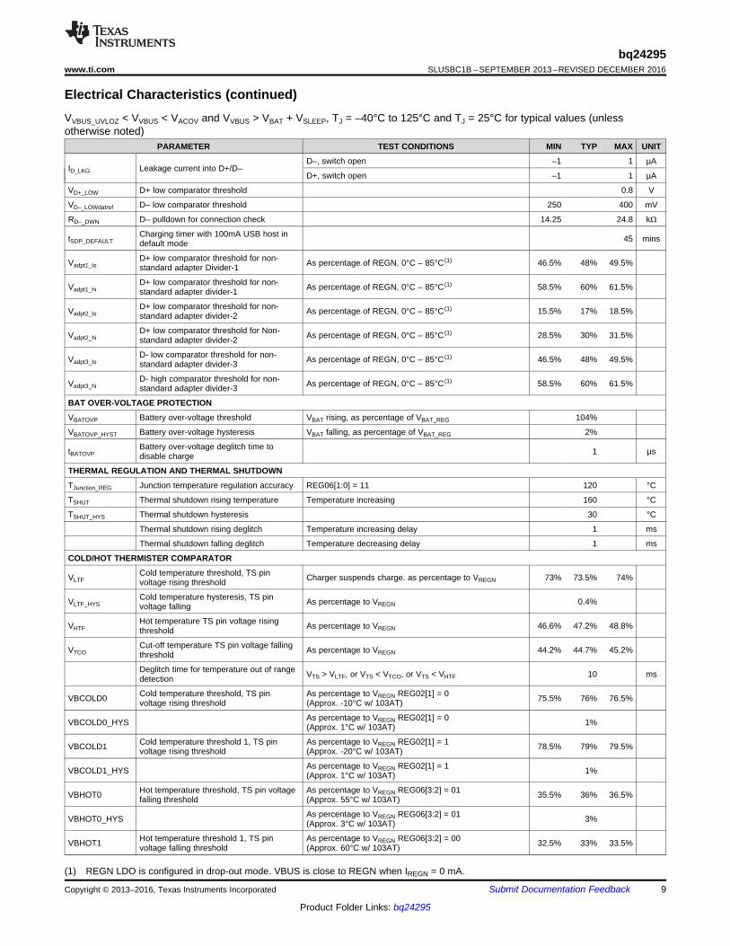
Electrical Characteristics (continued)VVBUS_UVLOZ < VVBUS < VACOV and VVBUS > VBAT + VSLEEP, TJ = –40°C to 125°C and TJ = 25°C for typical values (unlessotherwise noted)
PARAMETER TEST CONDITIONS MIN TYP MAX UNIT
VVBUSMIN Bad adapter detection threshold VVBUS falling 3.8 V
IBADSRC Bad adapter detection current source 30 mA
POWER PATH MANAGEMENT
VSYS_MAX Typical system regulation voltage Isys = 0 A, BATFET (Q4) off, VBAT up to 4.2 V,REG01[3:1] = 101, VSYSMIN = 3.5 V 3.5 4.35 V
VSYS_MIN System voltage outpu REG01[3:1] = 101, VSYSMIN = 3.5 V 3.5 3.65 V
RON(RBFET)Top reverse blocking MOSFET on-resistance between VBUS and PMIID 28 41 mΩ
RON(HSFET)Internal top switching MOSFET on-resistance between PMID and SW
TJ = –40°C – 85°C 39 51mΩ
TJ = -40°C – 125°C 39 58
RON(LSFET)Internal bottom switching MOSFET on-resistance between SW and PGND
TJ = –40°C – 85°C 61 82mΩ
TJ = -40°C – 125°C 61 90
VFWDBATFET forward voltage in supplementmode BAT discharge current 10mA 30 mV
VSYS_BAT SYS/BAT comparator VSYS falling 70 mV
VBATGD Battery good comparator rising threshold VBAT rising 3.55 V
VBATGD_HYST Battery good comparator falling threshold VBAT falling 100 mV
BATTERY CHARGER
VBAT_REG_ACC Charge voltage regulation accuracy VBAT = 4.112 V and 4.208 V –0.5% 0.5%
IICHG_REG_ACC Fast charge current regulation accuracy
VBAT = 3.8 V, ICHG = 1024 mA, TJ = 25°C -4% 4%
VBAT = 3.8 V, ICHG = 1024 mA, TJ = -20°C – 125°C -7% 7%
VBAT = 3.8 V, ICHG = 1792 mA, TJ = -20°C – 125°C –10% 10%
ICHG_20pct Charge current with 20% option on VBAT = 3.1 V, ICHG = 104 mA, REG02 = 03 and REG02[0]= 1 75 175 mA
VBATLOWV Battery LOWV falling threshold Fast charge to precharge, REG04[1] = 1 2.6 2.8 2.9 V
VBATLOWV_HYST Battery LOWV rising threshold Precharge to fast charge, REG04[1] = 1(Typical 200-mV hysteresis) 2.8 3.0 3.1 V
IPRECHG_ACC Precharge current regulation accuracy VBAT = 2.6 V, ICHG = 256 mA –20% 20%
ITYP_TERM_ACC Typical termination current ITERM = 256 mA, ICHG = 2048 mA 265 mA
ITERM_ACC Termination current accuracy ITERM = 256 mA, ICHG = 2048 mA –22.5% 22.5%
VSHORT Battery short voltage VBAT falling 2.0 V
VSHORT_HYST Battery Short Voltage hysteresis VBAT rising 200 mV
ISHORT Battery short current VBAT < 2.2 V 100 mA
VRECHG Recharge threshold below VBAT_REG VBAT falling, REG04[0] = 0 100 mV
tRECHG Recharge deglitch time VBAT falling, REG04[0] = 0 20 ms
RON_BATFET SYS-BAT MOSFET on-resistanceTJ = 25°C 24 28
mΩTJ = –40°C – 125°C 24 35
INPUT VOLTAGE/CURRENT REGULATION
VINDPM_REG_ACC Input voltage regulation accuracy -2% 2%
IUSB_DPMUSB Input current regulation limit, VBUS =5V, current pulled from SW
USB100 85 100 mA
USB150 125 150 mA
USB500 440 500 mA
USB900 750 900 mA
IADPT_DPM Input current regulation accuracy IADP = 1.5 A, REG00[2:0] = 101 1.3 1.5 A
IIN_START Input current limit during system start up VSYS < 2.2 V 100 mA
KILIM IIN = KILIM/RILIM IINDPM = 1.5 A 395 435 475 A x Ω
D+/D- DETECTION
VD+_SRC D+ voltage source 0.5 0.7 V
ID+_SRC D+ connection check current source 7 14 µA
ID–_SINK D– current sink 50 100 150 µA
9
bq24295www.ti.com SLUSBC1B –SEPTEMBER 2013–REVISED DECEMBER 2016
Product Folder Links: bq24295
Submit Documentation FeedbackCopyright © 2013–2016, Texas Instruments Incorporated
Electrical Characteristics (continued)VVBUS_UVLOZ < VVBUS < VACOV and VVBUS > VBAT + VSLEEP, TJ = –40°C to 125°C and TJ = 25°C for typical values (unlessotherwise noted)
PARAMETER TEST CONDITIONS MIN TYP MAX UNIT
(1) REGN LDO is configured in drop-out mode. VBUS is close to REGN when IREGN = 0 mA.
ID_LKG Leakage current into D+/D–D–, switch open –1 1 µA
D+, switch open –1 1 µA
VD+_LOW D+ low comparator threshold 0.8 V
VD–_LOWdatref D– low comparator threshold 250 400 mV
RD–_DWN D– pulldown for connection check 14.25 24.8 kΩ
tSDP_DEFAULTCharging timer with 100mA USB host indefault mode 45 mins
Vadpt1_loD+ low comparator threshold for non-standard adapter Divider-1 As percentage of REGN, 0°C – 85°C (1) 46.5% 48% 49.5%
Vadpt1_hiD+ low comparator threshold for non-standard adapter divider-1 As percentage of REGN, 0°C – 85°C (1) 58.5% 60% 61.5%
Vadpt2_loD+ low comparator threshold for non-standard adapter divider-2 As percentage of REGN, 0°C – 85°C (1) 15.5% 17% 18.5%
Vadpt2_hiD+ low comparator threshold for Non-standard adapter divider-2 As percentage of REGN, 0°C – 85°C (1) 28.5% 30% 31.5%
Vadpt3_loD- low comparator threshold for non-standard adapter divider-3 As percentage of REGN, 0°C – 85°C (1) 46.5% 48% 49.5%
Vadpt3_hiD- high comparator threshold for non-standard adapter divider-3 As percentage of REGN, 0°C – 85°C (1) 58.5% 60% 61.5%
BAT OVER-VOLTAGE PROTECTION
VBATOVP Battery over-voltage threshold VBAT rising, as percentage of VBAT_REG 104%
VBATOVP_HYST Battery over-voltage hysteresis VBAT falling, as percentage of VBAT_REG 2%
tBATOVPBattery over-voltage deglitch time todisable charge 1 µs
THERMAL REGULATION AND THERMAL SHUTDOWN
TJunction_REG Junction temperature regulation accuracy REG06[1:0] = 11 120 °C
TSHUT Thermal shutdown rising temperature Temperature increasing 160 °C
TSHUT_HYS Thermal shutdown hysteresis 30 °C
Thermal shutdown rising deglitch Temperature increasing delay 1 ms
Thermal shutdown falling deglitch Temperature decreasing delay 1 ms
COLD/HOT THERMISTER COMPARATOR
VLTFCold temperature threshold, TS pinvoltage rising threshold Charger suspends charge. as percentage to VREGN 73% 73.5% 74%
VLTF_HYSCold temperature hysteresis, TS pinvoltage falling As percentage to VREGN 0.4%
VHTFHot temperature TS pin voltage risingthreshold As percentage to VREGN 46.6% 47.2% 48.8%
VTCOCut-off temperature TS pin voltage fallingthreshold As percentage to VREGN 44.2% 44.7% 45.2%
Deglitch time for temperature out of rangedetection VTS > VLTF, or VTS < VTCO, or VTS < VHTF 10 ms
VBCOLD0 Cold temperature threshold, TS pinvoltage rising threshold
As percentage to VREGN REG02[1] = 0(Approx. -10°C w/ 103AT) 75.5% 76% 76.5%
VBCOLD0_HYS As percentage to VREGN REG02[1] = 0(Approx. 1°C w/ 103AT) 1%
VBCOLD1 Cold temperature threshold 1, TS pinvoltage rising threshold
As percentage to VREGN REG02[1] = 1(Approx. -20°C w/ 103AT) 78.5% 79% 79.5%
VBCOLD1_HYS As percentage to VREGN REG02[1] = 1(Approx. 1°C w/ 103AT) 1%
VBHOT0 Hot temperature threshold, TS pin voltagefalling threshold
As percentage to VREGN REG06[3:2] = 01(Approx. 55°C w/ 103AT) 35.5% 36% 36.5%
VBHOT0_HYS As percentage to VREGN REG06[3:2] = 01(Approx. 3°C w/ 103AT) 3%
VBHOT1 Hot temperature threshold 1, TS pinvoltage falling threshold
As percentage to VREGN REG06[3:2] = 00(Approx. 60°C w/ 103AT) 32.5% 33% 33.5%
10
bq24295SLUSBC1B –SEPTEMBER 2013–REVISED DECEMBER 2016 www.ti.com
Product Folder Links: bq24295
Submit Documentation Feedback Copyright © 2013–2016, Texas Instruments Incorporated
Electrical Characteristics (continued)VVBUS_UVLOZ < VVBUS < VACOV and VVBUS > VBAT + VSLEEP, TJ = –40°C to 125°C and TJ = 25°C for typical values (unlessotherwise noted)
PARAMETER TEST CONDITIONS MIN TYP MAX UNIT
VBHOT1_HYS As percentage to VREGN REG06[3:2] = 00(Approx. 3°C w/ 103AT) 3%
VBHOT2 Hot temperature threshold 2, TS pinvoltage falling threshold
As percentage to VREGN REG06[3:2] = 10(Approx. 65°C w/ 103AT) 29.5% 30% 30.5%
VBHOT2_HYS As percentage to VREGN REG06[3:2] = 10(Approx. 3°C w/ 103AT) 3%
CHARGE OVER-CURRENT COMPARATOR
IHSFET_OCPHSFET cycle by cycle over-currentthreshold 5.3 7.5 A
IBATFET_OCP System over load threshold 5.5 6.6 A
VLSFET_UCPLSFET charge under-current fallingthreshold From sync mode to non-sync mode 100 mA
FSWPWM Switching frequency, and digitalclock 1300 1500 1700 kHz
DMAX Maximum PWM duty cycle 97%
VBTST_REFRESH Bootstrap refresh comparator threshold VBTST-VSW when LSFET refresh pulse is requested,VBUS = 5 V 3.6 V
BOOST MODE OPERATION
VOTG_REG Boost mode output voltage I(PMID) = 0, REG06[7:4] = 1001 (5.126 V) 5.12 V
VOTG_REG_ACC Boost mode output voltage accuracy I(PMID) = 0, REG06[7:4] = 1001 (5.126 V) -3% 3%
VOTG_BAT Battery voltage exiting boost mode BAT falling, REG04[1] = 1 2.9 V
IOTG Boost mode output current on PMID 1.3 A
VOTG_OVP OTG over-voltage threshold Rising threshold 5.8 6 V
VOTG_OVP_HYS OTG over-voltage threshold hysteresis Falling threshold 300 mV
IOTG_LSOCP LSFET cycle by cycle current limit 5 A
IOTG_HSZCP HSFET under current falling threshold 100 mA
REGN LDO
VREGN REGN LDO output voltageVVBUS = 6 V, IREGN = 40 mA 4.8 5 5.5 V
VVBUS = 5 V, IREGN = 20 mA 4.7 4.8 V
IREGN REGN LDO current limit VVBUS = 5 V, VREGN = 3.8 V 50 mA
LOGIC I/O PIN CHARACTERISTICS (OTG, CE, STAT, QON)
VILO Input low threshold 0.4 V
VIH Input high threshold (CE, STAT, QON) 1.3 V
VIH_OTG Input high threshold (OTG) 1.1 V
VOUT_LO Output low saturation voltage Sink current = 5 mA 0.4 V
IBIASHigh level leakage current (OTG, CE,STAT ) Pull-up rail 1.8 V 1 µA
IBIAS High level leakage current (QON) Pull-up rail 3.6 V 8 µA
I2C INTERFACE (SDA, SCL, INT)
VIH Input high threshold level VPULL-UP = 1.8 V, SDA and SCL 1.3 V
VIL Input low threshold level VPULL-UP = 1.8 V, SDA and SCL 0.4 V
VOL Output low threshold level Sink current = 5 mA 0.4 V
IBIAS High-level leakage current VPULL-UP = 1.8 V, SDA and SCL 1 µA
fSCL SCL clock frequency 400 kHz
DIGITAL CLOCK AND WATCHDOG TIMER
fHIZ Digital crude clock REGN LDO disabled 15 35 50 kHz
fDIG Digital clock REGN LDO enabled 1300 1500 1700 kHz
11
bq24295www.ti.com SLUSBC1B –SEPTEMBER 2013–REVISED DECEMBER 2016
Product Folder Links: bq24295
Submit Documentation FeedbackCopyright © 2013–2016, Texas Instruments Incorporated
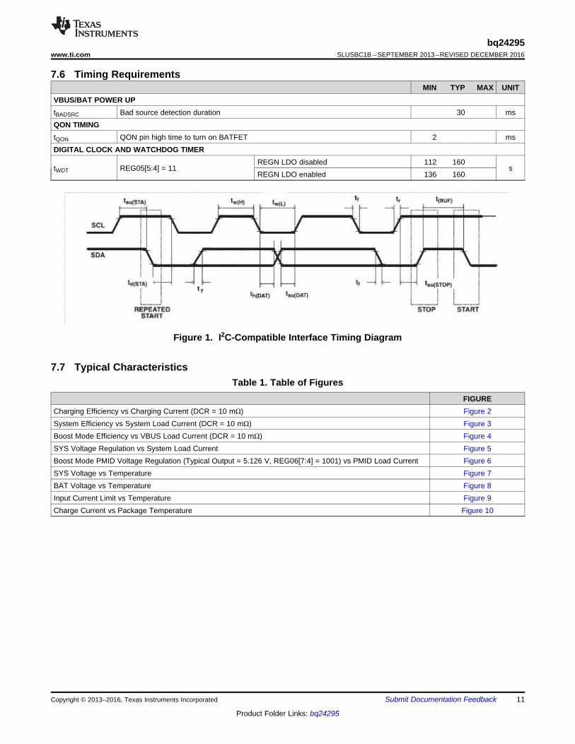
7.6 Timing RequirementsMIN TYP MAX UNIT
VBUS/BAT POWER UPtBADSRC Bad source detection duration 30 msQON TIMINGtQON QON pin high time to turn on BATFET 2 msDIGITAL CLOCK AND WATCHDOG TIMER
tWDT REG05[5:4] = 11REGN LDO disabled 112 160
sREGN LDO enabled 136 160
Figure 1. I2C-Compatible Interface Timing Diagram
7.7 Typical CharacteristicsTable 1. Table of Figures
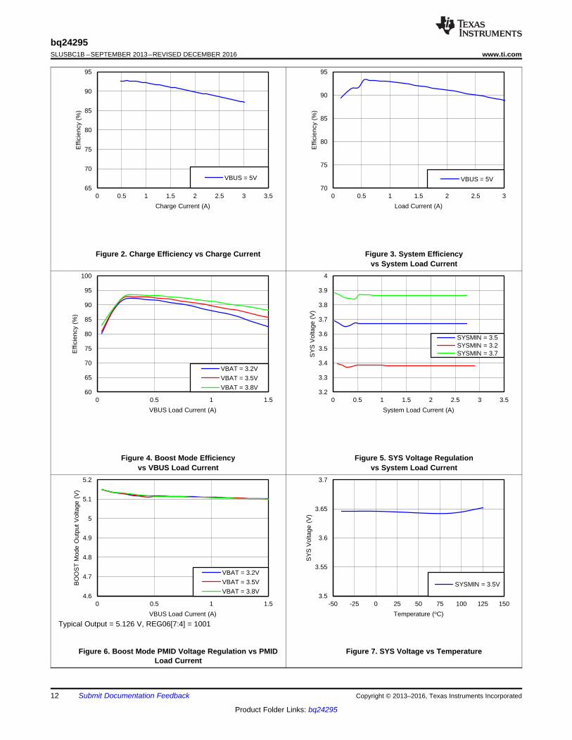
FIGURECharging Efficiency vs Charging Current (DCR = 10 mΩ) Figure 2System Efficiency vs System Load Current (DCR = 10 mΩ) Figure 3Boost Mode Efficiency vs VBUS Load Current (DCR = 10 mΩ) Figure 4SYS Voltage Regulation vs System Load Current Figure 5Boost Mode PMID Voltage Regulation (Typical Output = 5.126 V, REG06[7:4] = 1001) vs PMID Load Current Figure 6SYS Voltage vs Temperature Figure 7BAT Voltage vs Temperature Figure 8Input Current Limit vs Temperature Figure 9Charge Current vs Package Temperature Figure 10
4.6
4.7
4.8
4.9
5
5.1
5.2
0 0.5 1 1.5
BO
OS
T M
ode
Out
put
Vol
tage
(V
)
VBUS Load Current (A)
VBAT = 3.2V
VBAT = 3.5V
VBAT = 3.8V 3.5
3.55
3.6
3.65
3.7
-50 -25 0 25 50 75 100 125 150
SY
S V
olta
ge (
V)
Temperature (oC)
SYSMIN = 3.5V
60
65
70
75
80
85
90
95
100
0 0.5 1 1.5
Effi
cien
cy (
%)
VBUS Load Current (A)
VBAT = 3.2V
VBAT = 3.5V
VBAT = 3.8V 3.2
3.3
3.4
3.5
3.6
3.7
3.8
3.9
4
0 0.5 1 1.5 2 2.5 3 3.5
SY
S V
olta
ge (
V)
System Load Current (A)
SYSMIN = 3.5 SYSMIN = 3.2 SYSMIN = 3.7
65
70
75
80
85
90
95
0 0.5 1 1.5 2 2.5 3 3.5
Effi
cien
cy (
%)
Charge Current (A)
VBUS = 5V
70
75
80
85
90
95
0 0.5 1 1.5 2 2.5 3
Effi
cien
cy (
%)
Load Current (A)
VBUS = 5V
12
bq24295SLUSBC1B –SEPTEMBER 2013–REVISED DECEMBER 2016 www.ti.com
Product Folder Links: bq24295
Submit Documentation Feedback Copyright © 2013–2016, Texas Instruments Incorporated
Figure 2. Charge Efficiency vs Charge Current Figure 3. System Efficiencyvs System Load Current
Figure 4. Boost Mode Efficiencyvs VBUS Load Current
Figure 5. SYS Voltage Regulationvs System Load Current
Typical Output = 5.126 V, REG06[7:4] = 1001
Figure 6. Boost Mode PMID Voltage Regulation vs PMIDLoad Current
Figure 7. SYS Voltage vs Temperature
0
0.5
1
1.5
2
2.5
60 80 100 120 140 160
Cha
rge
Cur
rent
(A
)
Package Temperature (oC)
TREG = 120C TREG = 80C
4.1
4.15
4.2
4.25
4.3
4.35
4.4
-50 -25 0 25 50 75 100 125 150
BA
T V
olta
ge (
V)
Temperature (oC)
VREG = 4.208V
VREG = 4.35V 0
0.5
1
1.5
2
2.5
-50 -25 0 25 50 75 100 125 150
Inpu
t C
urre
nt L
imit
(A)
Temperature (oC)
IIN = 500mA
IIN = 1.5A
IIN = 2A
13
bq24295www.ti.com SLUSBC1B –SEPTEMBER 2013–REVISED DECEMBER 2016
Product Folder Links: bq24295
Submit Documentation FeedbackCopyright © 2013–2016, Texas Instruments Incorporated
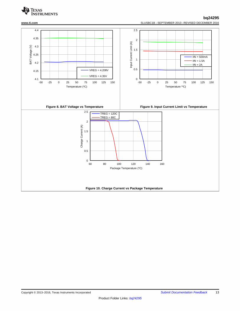
Figure 8. BAT Voltage vs Temperature Figure 9. Input Current Limit vs Temperature
Figure 10. Charge Current vs Package Temperature
14
bq24295SLUSBC1B –SEPTEMBER 2013–REVISED DECEMBER 2016 www.ti.com
Product Folder Links: bq24295
Submit Documentation Feedback Copyright © 2013–2016, Texas Instruments Incorporated
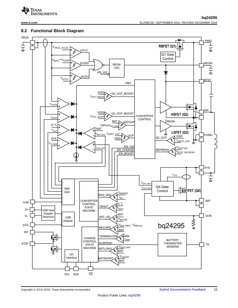
8 Detailed Description
8.1 OverviewThe bq24295 is an I2C controlled power path management device and a single cell Li-Ion battery charger. Itintegrates the input reverse-blocking FET (RBFET, Q1), high-side switching FET (HSFET, Q2), low-sideswitching FET (LSFET, Q3), and battery FET (BATFET, Q4) between system and battery. The device alsointegrates the bootstrap diode for the high-side gate drive.
STAT
SCL SDA
FBO
CONVERTER
CONTROL
PGND
REGN
BTST
REGN
TSHUTTSHUT
IC TJ
TS
REGN
LDO
bq24295
PMID
RBFET (Q1)
VBUS
LSFET (Q3)
HSFET (Q2)
SW
BATFET (Q4)
SYS
BAT
CHARGE
CONTROL
STATE
MACHINE
I2C
Interface
INT
IINDPM
ICHG_REG
VSYSMIN
VBAT_REG
IC TJ
TREG
BATLOWVBAT
VBATLOWV
SUSPEND
RECHRGBAT
V - VBAT_REG RECHG
REFRESHVBTST_REFRESH
UCPILSFET_UCP
I(Q3)
BATOVP104%xVBAT_REG
BAT
VINDPM
D+
D–
USB Host
Adapter
Detection
OTG
EN_CHARGE
EN_BOOST
BAD_SRCIBADSRC
IDC
BAT_GDVBATGD
BAT
EN_HIZ
USB
Adapter
TERMINATIONITERM
ICHG
BATSHORTBAT
VSHORT
CONVERTER
CONTROL
STATE
MACHINE
Q2_OCPIHSFET_OCP
I(Q2)SYS
BAT
REF
DAC
ICHG_REG
VVBUS_UVLOZ
UVLO
SLEEP
VACOVACOV
EN_HIZ
CE
ILIM
ICHG
VBAT_REG
Q4 Gate
Control
Q3_OCP_BOOSTI(Q3)
Q2_UCP_BOOSTIOTG_HSZCP
I(Q2)
BATTERY
THERMISTER
SENSING
Q1 Gate
Control
QON
VBATZ+VSLEEP
IOTG_LSOCP
VBTST-SW
15
bq24295www.ti.com SLUSBC1B –SEPTEMBER 2013–REVISED DECEMBER 2016
Product Folder Links: bq24295
Submit Documentation FeedbackCopyright © 2013–2016, Texas Instruments Incorporated
8.2 Functional Block Diagram
QON
BATFET Status
Turn off by i2c commandREG07[5]=1
Min. 2ms
Turn on by QONREG07[5]=0
16
bq24295SLUSBC1B –SEPTEMBER 2013–REVISED DECEMBER 2016 www.ti.com
Product Folder Links: bq24295
Submit Documentation Feedback Copyright © 2013–2016, Texas Instruments Incorporated
8.3 Feature Description
8.3.1 Device Power Up
8.3.1.1 Power-On-Reset (POR)The internal bias circuits are powered from the higher voltage of VBUS and BAT. When VBUS or VBAT risesabove UVLOZ, the sleep comparator, battery depletion comparator and BATFET driver are active. I2C interfaceis ready for communication and all the registers are reset to default value. The host can access all the registersafter POR.
8.3.1.2 Power Up from Battery without DC SourceIf only battery is present and the voltage is above depletion threshold (VBAT_DEPL), the BATFET turns on andconnects battery to system. The REGN LDO stays off to minimize the quiescent current. The low RDSON inBATFET and the low quiescent current on BAT minimize the conduction loss and maximize the battery run time.During both boost and charge mode, the device always monitors the discharge current through BATFET. Whenthe system is overloaded or shorted, the device will immediately turn off BATFET and keep BATFET off until theinput source plugs in again.
8.3.1.2.1 BATFET Turn Off
The BATFET can be forced off by the host through I2C REG07[5]. This bit allows the user to independently turnoff the BATFET when the battery condition becomes abnormal during charging. When BATFET is off, there is nopath to charge or discharge the battery. When battery is not attached, the BATFET should be turned off bysetting REG07[5] to 1 to disable charging and supplement mode.
8.3.1.2.2 Shipping Mode
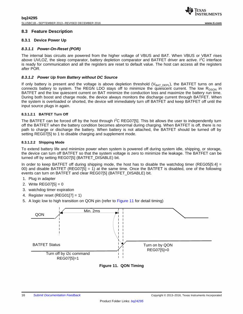
To extend battery life and minimize power when system is powered off during system idle, shipping, or storage,the device can turn off BATFET so that the system voltage is zero to minimize the leakage. The BATFET can beturned off by setting REG07[5] (BATFET_DISABLE) bit.
In order to keep BATFET off during shipping mode, the host has to disable the watchdog timer (REG05[5:4] =00) and disable BATFET (REG07[5] = 1) at the same time. Once the BATFET is disabled, one of the followingevents can turn on BATFET and clear REG07[5] (BATFET_DISABLE) bit.1. Plug in adapter2. Write REG07[5] = 03. watchdog timer expiration4. Register reset (REG01[7] = 1)5. A logic low to high transition on QON pin (refer to Figure 11 for detail timing)
Figure 11. QON Timing
17
bq24295www.ti.com SLUSBC1B –SEPTEMBER 2013–REVISED DECEMBER 2016
Product Folder Links: bq24295
Submit Documentation FeedbackCopyright © 2013–2016, Texas Instruments Incorporated
Feature Description (continued)8.3.1.3 Boost Mode Operation from BatteryThe device supports boost converter operation to deliver power from the battery to other portable devicesthrough PMID pin. The boost mode output current rating meets the 1.5-A charging requirements for smartphoneand tablet. The boost operation is enabled by default if the conditions are valid:1. BAT above BATLOWV threshold (VBATLOWV set by REG04[1])2. VBUS less than BAT+VSLEEP (in sleep mode)3. Boost mode operation is enabled (OTG pin HIGH and REG01[5:4] = 10)4. After 30ms delay from boost mode enable
In battery boost mode, the device employs a 1.5-MHz step-up switching regulator. During boost mode, the statusregister REG08[7:6] is set to 11, the PMID output voltage is 5.1 V. In addition, the device provides adjustableboost voltage from 4.55 V to 5.5 V by changing BOOSTV bits in REG06[7:4]. Any fault during boost operation,including PMID over-voltage, sets the fault register REG09[6] to 1 and an INT is asserted.
For power bank applications, the boost current is supported from PMID pin as in the application diagram. It isrecommended to use the minimum PMID cap value 20 uF for boost current. Please note that there is no boostcurrent limit setting when the boost current is sourced from PMID pin, hence it is important not to overload theboost current under this condition.
8.3.1.3.1 Integrated Control to Switch Between USB Charge Mode and Boost Mode
The device features integrated control to switch between charge mode and boost mode by monitoring VBUSvoltage. When VBUS is higher than VBAT+VSLEEP , the RBFET is enabled and charge mode is enabled. WhenVBUS power source is removed, the RBFET is automatically turn off to isolate VBUS from PMID. The boostmode is started when the conditions described above are met.
8.3.1.4 Power Up from DC SourceWhen the DC source plugs in, the charger device checks the input source voltage to turn on REGN LDO and allthe bias circuits. It also checks the input current limit before starts the buck converter.
8.3.1.4.1 REGN LDO
The REGN LDO supplies internal bias circuits as well as the HSFET and LSFET gate drive. The LDO alsoprovides bias rail to TS external resistors. The pull-up rail of STAT can be connected to REGN as well.
The REGN is enabled when all the conditions are valid.1. VBUS above VVBUS_UVLOZ
2. VBUS above VBAT + VSLEEPZ in buck mode or VBUS below VBAT + VSLEEP in boost mode3. After typical 220-ms delay (100 ms minimum) is complete
If one of the above conditions is not valid, the device is in high impedance mode (HIZ) with REGN LDO off. Thedevice draws less than IVBUS (15 µA typical) from VBUS during HIZ state. The battery powers up the systemwhen the device is in HIZ.
8.3.1.4.2 Input Source Qualification
After REGN LDO powers up, the device checks the current capability of the input source. The input source hasto meet the following requirements to start the buck converter.1. VBUS voltage below VACOV (not in VBUS over-voltage)2. VBUS voltage above VBADSRC (3.8 V typical) when pulling IBADSRC (30 mA typical) (poor source detection)
Once the input source passes all the conditions above, the status register REG08[2] goes high. An INT isasserted to the host.
If the device fails the poor source detection, it will repeat the detection every 2 seconds.
D+
D-
VDP_SRC
VLGC_HI
IDP_SRC
CHG_DETVDAC_REF
IDM_SINK
RDM_DWN
18
bq24295SLUSBC1B –SEPTEMBER 2013–REVISED DECEMBER 2016 www.ti.com
Product Folder Links: bq24295
Submit Documentation Feedback Copyright © 2013–2016, Texas Instruments Incorporated
Feature Description (continued)8.3.1.4.3 Input Current Limit Detection
The USB ports on personal computers are convenient charging source for portable devices (PDs). If the portabledevice is attached to a USB host, the USB specification requires the portable device to draw limited current (500mA in USB 2.0, and 150 mA/900 mA in USB 3.0). If the portable device is attached to a charging port, it isallowed to draw up to 3 A.
After the REG08[2] goes HIGH, the charger device always runs input current limit detection when a DC sourceplugs in unless the charger is in HIZ during host mode.
The bq24295 follows Battery Charging Specification 1.2 (BC1.2) to detect input source through USB D+/D- lines.After the input current limit detection is done, the detection result is reported in VBUS_STAT registers(REG08[7:6]) and input current limit is updated in IINLIM register (REG00[2:0]). In addition, host can write toREG00[2:0] to change the input current limit.
8.3.1.4.4 D+/D– Detection Sets Input Current Limit
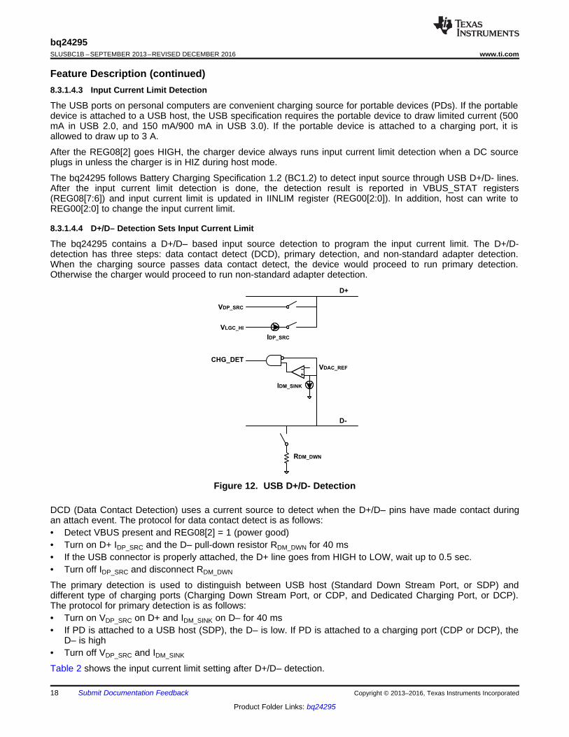
The bq24295 contains a D+/D– based input source detection to program the input current limit. The D+/D-detection has three steps: data contact detect (DCD), primary detection, and non-standard adapter detection.When the charging source passes data contact detect, the device would proceed to run primary detection.Otherwise the charger would proceed to run non-standard adapter detection.
Figure 12. USB D+/D- Detection
DCD (Data Contact Detection) uses a current source to detect when the D+/D– pins have made contact duringan attach event. The protocol for data contact detect is as follows:• Detect VBUS present and REG08[2] = 1 (power good)• Turn on D+ IDP_SRC and the D– pull-down resistor RDM_DWN for 40 ms• If the USB connector is properly attached, the D+ line goes from HIGH to LOW, wait up to 0.5 sec.• Turn off IDP_SRC and disconnect RDM_DWN
The primary detection is used to distinguish between USB host (Standard Down Stream Port, or SDP) anddifferent type of charging ports (Charging Down Stream Port, or CDP, and Dedicated Charging Port, or DCP).The protocol for primary detection is as follows:• Turn on VDP_SRC on D+ and IDM_SINK on D– for 40 ms• If PD is attached to a USB host (SDP), the D– is low. If PD is attached to a charging port (CDP or DCP), the
D– is high• Turn off VDP_SRC and IDM_SINK
Table 2 shows the input current limit setting after D+/D– detection.
19
bq24295www.ti.com SLUSBC1B –SEPTEMBER 2013–REVISED DECEMBER 2016
Product Folder Links: bq24295
Submit Documentation FeedbackCopyright © 2013–2016, Texas Instruments Incorporated
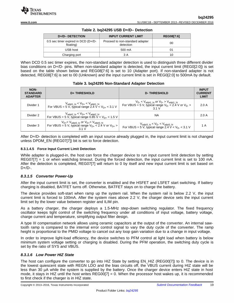
Table 2. bq24295 USB D+/D– DetectionD+/D– DETECTION INPUT CURRENT LIMIT REG08[7:6]
0.5 sec timer expired in DCD (D+/D-floating)
Proceed to non-standard adapterdetection 00
USB host 500 mA 01Charging port 3 A 10
When DCD 0.5 sec timer expires, the non-standard adapter detection is used to distinguish three different dividerbias conditions on D+/D- pins. When non-standard adapter is detected, the input current limit (REG0[2:0]) is setbased on the table shown below and REG08[7:6] is set to 10 (Adapter port). If non-standard adapter is notdetected, REG08[7:6] is set to 00 (Unknown) and the input current limit is set in REG0[2:0] to 500mA by default.
Table 3. bq24295 Non-Standard Adapter DetectionNON-
STANDARDADAPTER
D+ THRESHOLD D- THRESHOLDINPUT
CURRENTLIMIT
Divider 1 Vadpt1_lo < VD+ < Vadpt1_hiFor VBUS = 5 V, typical range 2.4 V < VD+ < 3.1 V
VD- < Vadpt1_lo or VD- > Vadpt1_hiFor VBUS = 5 V, typical range VD- < 2.4 V or VD- >
3.1 V2.0 A
Divider 2 Vadpt2_lo < VD+ < Vadpt2_hiFor VBUS = 5 V, typical range 0.85 V < VD+ < 1.5 V NA 2.0 A
Divider 3VD+< Vadpt3_lo or VD+> Vadpt3_hi
For VBUS = 5 V, typical range VD+ < 2.4 V or VD+ >3.1 V
Vadpt3_lo < VD- < Vadpt3_hiFor VBUS = 5 V, typical range 2.4 V < VD- < 3.1 V 1 A
After D+/D- detection is completed with an input source already plugged in, the input current limit is not changedunless DPDM_EN (REG07[7]) bit is set to force detection.
8.3.1.4.5 Force Input Current Limit Detection
While adapter is plugged-in, the host can force the charger device to run input current limit detection by settingREG07[7] = 1 or when watchdog timeout. During the forced detection, the input current limit is set to 100 mA.After the detection is completed, REG07[7] will return to 0 by itself and new input current limit is set based onD+/D-.
8.3.1.5 Converter Power-UpAfter the input current limit is set, the converter is enabled and the HSFET and LSFET start switching. If batterycharging is disabled, BATFET turns off. Otherwise, BATFET stays on to charge the battery.
The device provides soft-start when ramp up the system rail. When the system rail is below 2.2 V, the inputcurrent limit is forced to 100mA. After the system rises above 2.2 V, the charger device sets the input currentlimit set by the lower value between register and ILIM pin.
As a battery charger, the charger deploys a 1.5-MHz step-down switching regulator. The fixed frequencyoscillator keeps tight control of the switching frequency under all conditions of input voltage, battery voltage,charge current and temperature, simplifying output filter design.
A type III compensation network allows using ceramic capacitors at the output of the converter. An internal saw-tooth ramp is compared to the internal error control signal to vary the duty cycle of the converter. The rampheight is proportional to the PMID voltage to cancel out any loop gain variation due to a change in input voltage.
In order to improve light-load efficiency, the device switches to PFM control at light load when battery is belowminimum system voltage setting or charging is disabled. During the PFM operation, the switching duty cycle isset by the ratio of SYS and VBUS.
8.3.1.6 Low Power HIZ StateThe host can configure the converter to go into HIZ State by setting EN_HIZ (REG00[7]) to 0. The device is inthe lowest quiescent state with REGN LDO and the bias circuits off, the VBUS current during HIZ state will beless than 30 µA while the system is supplied by the battery. Once the charger device enters HIZ state in hostmode, it stays in HIZ until the host writes REG00[7] = 0. When the processor host wakes up, it is recommendedto first check if the charger is in HIZ state.
2.7 2.9 3.1 3.3 3.5 3.7 3.9 4.1 4.3
BAT (V)
3.1
3.3
3.5
3.7
3.9
4.1
4.3
4.5
SYS
(V)
Charge Disabled
Charge Enabled
Minimum System Voltage
20
bq24295SLUSBC1B –SEPTEMBER 2013–REVISED DECEMBER 2016 www.ti.com
Product Folder Links: bq24295
Submit Documentation Feedback Copyright © 2013–2016, Texas Instruments Incorporated
8.3.2 Power Path ManagementThe device accommodates a wide range of input sources from USB, wall adapter, to car battery. The deviceprovides automatic power path selection to supply the system (SYS) from input source (VBUS), battery (BAT), orboth.
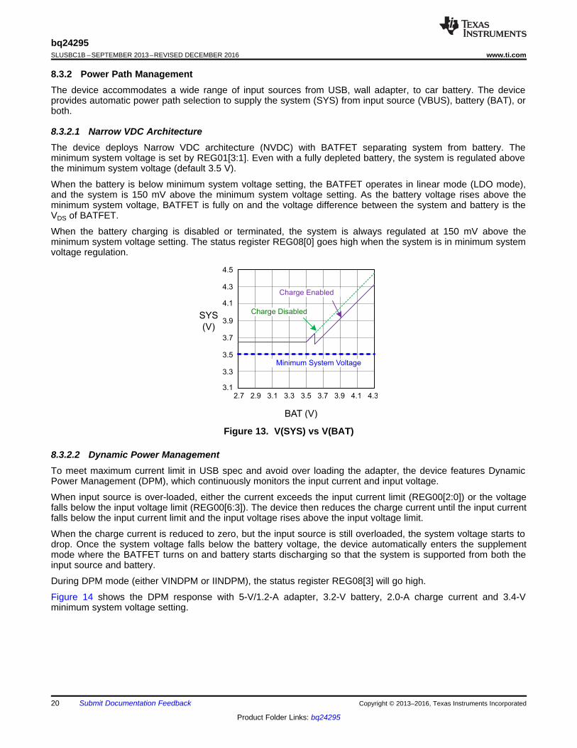
8.3.2.1 Narrow VDC ArchitectureThe device deploys Narrow VDC architecture (NVDC) with BATFET separating system from battery. Theminimum system voltage is set by REG01[3:1]. Even with a fully depleted battery, the system is regulated abovethe minimum system voltage (default 3.5 V).
When the battery is below minimum system voltage setting, the BATFET operates in linear mode (LDO mode),and the system is 150 mV above the minimum system voltage setting. As the battery voltage rises above theminimum system voltage, BATFET is fully on and the voltage difference between the system and battery is theVDS of BATFET.
When the battery charging is disabled or terminated, the system is always regulated at 150 mV above theminimum system voltage setting. The status register REG08[0] goes high when the system is in minimum systemvoltage regulation.
Figure 13. V(SYS) vs V(BAT)
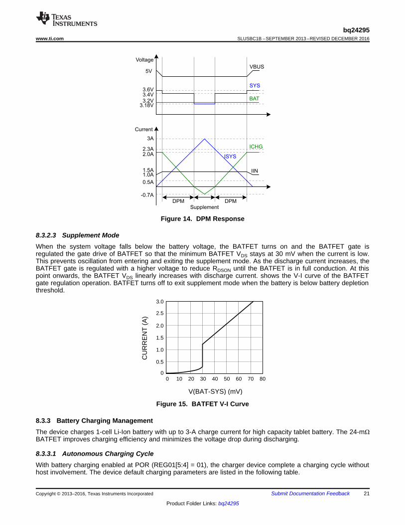
8.3.2.2 Dynamic Power ManagementTo meet maximum current limit in USB spec and avoid over loading the adapter, the device features DynamicPower Management (DPM), which continuously monitors the input current and input voltage.
When input source is over-loaded, either the current exceeds the input current limit (REG00[2:0]) or the voltagefalls below the input voltage limit (REG00[6:3]). The device then reduces the charge current until the input currentfalls below the input current limit and the input voltage rises above the input voltage limit.
When the charge current is reduced to zero, but the input source is still overloaded, the system voltage starts todrop. Once the system voltage falls below the battery voltage, the device automatically enters the supplementmode where the BATFET turns on and battery starts discharging so that the system is supported from both theinput source and battery.
During DPM mode (either VINDPM or IINDPM), the status register REG08[3] will go high.
Figure 14 shows the DPM response with 5-V/1.2-A adapter, 3.2-V battery, 2.0-A charge current and 3.4-Vminimum system voltage setting.
0 10 20 30 40 50 60 70 80
V(BAT-SYS) (mV)
0
0.5
1.0
1.5
2.0
2.5
3.0
CU
RR
EN
T (
A)
5V
Current
2.0A
3A
-0.7A
2.3A
0.5A
3.6V3.4V3.2V
3.18V
1.5A1.0A
DPM DPMSupplement
Voltage
SYS
VBUS
BAT
ICHG
IIN
ISYS
21
bq24295www.ti.com SLUSBC1B –SEPTEMBER 2013–REVISED DECEMBER 2016
Product Folder Links: bq24295
Submit Documentation FeedbackCopyright © 2013–2016, Texas Instruments Incorporated
Figure 14. DPM Response
8.3.2.3 Supplement ModeWhen the system voltage falls below the battery voltage, the BATFET turns on and the BATFET gate isregulated the gate drive of BATFET so that the minimum BATFET VDS stays at 30 mV when the current is low.This prevents oscillation from entering and exiting the supplement mode. As the discharge current increases, theBATFET gate is regulated with a higher voltage to reduce RDSON until the BATFET is in full conduction. At thispoint onwards, the BATFET VDS linearly increases with discharge current. shows the V-I curve of the BATFETgate regulation operation. BATFET turns off to exit supplement mode when the battery is below battery depletionthreshold.
Figure 15. BATFET V-I Curve
8.3.3 Battery Charging ManagementThe device charges 1-cell Li-Ion battery with up to 3-A charge current for high capacity tablet battery. The 24-mΩBATFET improves charging efficiency and minimizes the voltage drop during discharging.
8.3.3.1 Autonomous Charging CycleWith battery charging enabled at POR (REG01[5:4] = 01), the charger device complete a charging cycle withouthost involvement. The device default charging parameters are listed in the following table.
22
bq24295SLUSBC1B –SEPTEMBER 2013–REVISED DECEMBER 2016 www.ti.com
Product Folder Links: bq24295
Submit Documentation Feedback Copyright © 2013–2016, Texas Instruments Incorporated
(1) See Charging Safety Timer for more information.
Table 4. Charging Parameter Default SettingDEFAULT MODE bq24295Charging voltage 4.208 VCharging current 1.024 A
Pre-charge current 256 mATermination current 256 mATemperature profile Hot/Cold
Safety timer 12 hours (1)
A new charge cycle starts when the following conditions are valid:• Converter starts• Battery charging is enabled by I2C register bit (REG01[5:4]) = 01 and CE is low• No thermistor fault on TS• No safety timer fault• BATFET is not forced to turn off (REG07[5])
The charger device automatically terminates the charging cycle when the charging current is below terminationthreshold and charge voltage is above recharge threshold. When a full battery voltage is discharged belowrecharge threshold (REG04[0]), the device automatically starts another charging cycle. After the charge done,either toggle CE pin or REG01[5:4] will initiate a new charging cycle.
The STAT output indicates the charging status of charging (LOW), charging complete or charge disable (HIGH)or charging fault (Blinking). The status register REG08[5:4] indicates the different charging phases: 00-chargingdisable, 01-precharge, 10-fast charge (constant current) and constant voltage mode, 11-charging done. Once acharging cycle is complete, an INT is asserted to notify the host.
The host can always control the charging operation and optimize the charging parameters by writing to theregisters through I2C.
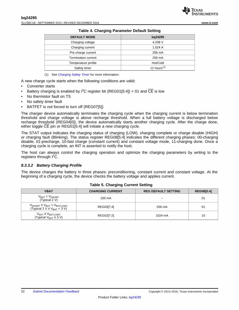
8.3.3.2 Battery Charging ProfileThe device charges the battery in three phases: preconditioning, constant current and constant voltage. At thebeginning of a charging cycle, the device checks the battery voltage and applies current.
Table 5. Charging Current SettingVBAT CHARGING CURRENT REG DEFAULT SETTING REG08[5:4]
VBAT < VSHORT(Typical 2 V) 100 mA – 01
VSHORT ≤ VBAT < VBATLOWV(Typical 2 V ≤ VBAT < 3 V) REG03[7:4] 256 mA 01
VBAT ≥ VBATLOWV(Typical VBAT ≥ 3 V) REG02[7:2] 1024 mA 10
Regulation Voltage
(3.5V – 4.4V)
Fast Charge Current
(500mA-3008mA)
VBAT_LOWV (2.8V/3V)
VBAT_SHORT (2V)
IPRECHARGE (128mA-2048mA)ITERMINATION (128mA-2048mA)
IBATSHORT (100mA)
Battery Voltage
Charge Current
Trickle Charge Pre-charge Fast Charge and Voltage Regulation Safety Timer
Expiration
23
bq24295www.ti.com SLUSBC1B –SEPTEMBER 2013–REVISED DECEMBER 2016
Product Folder Links: bq24295
Submit Documentation FeedbackCopyright © 2013–2016, Texas Instruments Incorporated
If the charger device is in DPM regulation or thermal regulation during charging, the actual charging current willbe less than the programmed value. In this case, termination is temporarily disabled and the charging safetytimer is counted at half the clock rate.
Figure 16. Battery Charging Profile
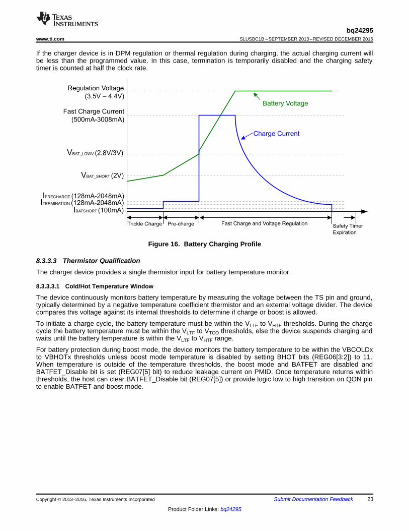
8.3.3.3 Thermistor QualificationThe charger device provides a single thermistor input for battery temperature monitor.
8.3.3.3.1 Cold/Hot Temperature Window
The device continuously monitors battery temperature by measuring the voltage between the TS pin and ground,typically determined by a negative temperature coefficient thermistor and an external voltage divider. The devicecompares this voltage against its internal thresholds to determine if charge or boost is allowed.
To initiate a charge cycle, the battery temperature must be within the VLTF to VHTF thresholds. During the chargecycle the battery temperature must be within the VLTF to VTCO thresholds, else the device suspends charging andwaits until the battery temperature is within the VLTF to VHTF range.
For battery protection during boost mode, the device monitors the battery temperature to be within the VBCOLDxto VBHOTx thresholds unless boost mode temperature is disabled by setting BHOT bits (REG06[3:2]) to 11.When temperature is outside of the temperature thresholds, the boost mode and BATFET are disabled andBATFET_Disable bit is set (REG07[5] bit) to reduce leakage current on PMID. Once temperature returns withinthresholds, the host can clear BATFET_Disable bit (REG07[5]) or provide logic low to high transition on QON pinto enable BATFET and boost mode.
Temperature Range toBoost
Boost DisableV BCOLDx
(-10ºC / -20ºC)
Boost Enable
VBHOTx
(55ºC / 60ºC / 65ºC)
Boost Disable
AGND
VREGN
TEMPERATURE RANGE TO
INITIATE CHARGE
TEMPERATURE RANGE
DURING A CHARGE CYCLE
CHARGE SUSPENDED CHARGE SUSPENDED
VREGN
VLTF
CHARGE at full C CHARGE at full C
VHTF
VTCO
CHARGE SUSPENDEDCHARGE SUSPENDED
AGND AGND
VLTFH VLTFH
VLTF
VREGN
REGN
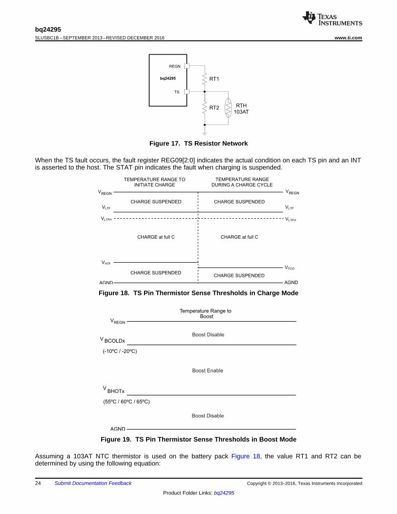
TS
RT2
RT1
RTH
103AT
bq24295
24
bq24295SLUSBC1B –SEPTEMBER 2013–REVISED DECEMBER 2016 www.ti.com
Product Folder Links: bq24295
Submit Documentation Feedback Copyright © 2013–2016, Texas Instruments Incorporated
Figure 17. TS Resistor Network
When the TS fault occurs, the fault register REG09[2:0] indicates the actual condition on each TS pin and an INTis asserted to the host. The STAT pin indicates the fault when charging is suspended.
Figure 18. TS Pin Thermistor Sense Thresholds in Charge Mode
Figure 19. TS Pin Thermistor Sense Thresholds in Boost Mode
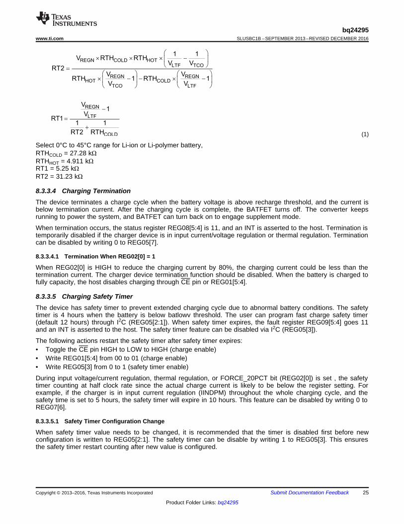
Assuming a 103AT NTC thermistor is used on the battery pack Figure 18, the value RT1 and RT2 can bedetermined by using the following equation:
REGN COLD HOT
LTF TCO
REGN REGNHOT COLD
TCO LTF
REGN
LTF
COLD
1 1V RTH RTH
V V RT2
V VRTH 1 RTH 1
V V
V1
VRT1
1 1
RT2 RTH
æ ö´ ´ ´ -ç ÷
è ø=æ ö æ ö
´ - - ´ -ç ÷ ç ÷è øè ø
-
=
+
25
bq24295www.ti.com SLUSBC1B –SEPTEMBER 2013–REVISED DECEMBER 2016
Product Folder Links: bq24295
Submit Documentation FeedbackCopyright © 2013–2016, Texas Instruments Incorporated
(1)
Select 0°C to 45°C range for Li-ion or Li-polymer battery,RTHCOLD = 27.28 kΩRTHHOT = 4.911 kΩRT1 = 5.25 kΩRT2 = 31.23 kΩ
8.3.3.4 Charging TerminationThe device terminates a charge cycle when the battery voltage is above recharge threshold, and the current isbelow termination current. After the charging cycle is complete, the BATFET turns off. The converter keepsrunning to power the system, and BATFET can turn back on to engage supplement mode.
When termination occurs, the status register REG08[5:4] is 11, and an INT is asserted to the host. Termination istemporarily disabled if the charger device is in input current/voltage regulation or thermal regulation. Terminationcan be disabled by writing 0 to REG05[7].
8.3.3.4.1 Termination When REG02[0] = 1
When REG02[0] is HIGH to reduce the charging current by 80%, the charging current could be less than thetermination current. The charger device termination function should be disabled. When the battery is charged tofully capacity, the host disables charging through CE pin or REG01[5:4].
8.3.3.5 Charging Safety TimerThe device has safety timer to prevent extended charging cycle due to abnormal battery conditions. The safetytimer is 4 hours when the battery is below batlowv threshold. The user can program fast charge safety timer(default 12 hours) through I2C (REG05[2:1]). When safety timer expires, the fault register REG09[5:4] goes 11and an INT is asserted to the host. The safety timer feature can be disabled via I2C (REG05[3]).
The following actions restart the safety timer after safety timer expires:• Toggle the CE pin HIGH to LOW to HIGH (charge enable)• Write REG01[5:4] from 00 to 01 (charge enable)• Write REG05[3] from 0 to 1 (safety timer enable)
During input voltage/current regulation, thermal regulation, or FORCE_20PCT bit (REG02[0]) is set , the safetytimer counting at half clock rate since the actual charge current is likely to be below the register setting. Forexample, if the charger is in input current regulation (IINDPM) throughout the whole charging cycle, and thesafety time is set to 5 hours, the safety timer will expire in 10 hours. This feature can be disabled by writing 0 toREG07[6].
8.3.3.5.1 Safety Timer Configuration Change
When safety timer value needs to be changed, it is recommended that the timer is disabled first before newconfiguration is written to REG05[2:1]. The safety timer can be disable by writing 1 to REG05[3]. This ensuresthe safety timer restart counting after new value is configured.
ILIMINMAX
VI IIN 1V
= ´
INMAX LIM
ILIM
1VI K
R= ´
26
bq24295SLUSBC1B –SEPTEMBER 2013–REVISED DECEMBER 2016 www.ti.com
Product Folder Links: bq24295
Submit Documentation Feedback Copyright © 2013–2016, Texas Instruments Incorporated
8.3.4 Status Outputs (STAT, and INT)
8.3.4.1 Charging Status Indicator (STAT)The device indicates charging state on the open drain STAT pin. The STAT pin can drive LED as the applicationdiagram shows.
Table 6. STAT Pin StateCHARGING STATE STAT
Charging in progress (including recharge) LOWCharging complete HIGHSleep mode, charge disable HIGH
8.3.4.2 Interrupt to Host (INT)In some applications, the host does not always monitor the charger operation. The INT notifies the system on thedevice operation. The following events will generate a 256-µs INT pulse.1. USB/adapter source identified (through DPDM detection)2. Good input source detected
– not in sleep– VBUS below VACOV threshold– current limit above IBADSRC
3. Input removed or VBUS above VACOV threshold4. Charge Complete5. Any FAULT event in REG09
For the first four events, INT pulse is always generated. For the last event, when a fault occurs, the chargerdevice sends out INT and latches the fault state in REG09 until the host reads the fault register. If a prior faultexists, the charger device would not send any INT upon new faults except NTC fault (REG09[2:0]). The NTCfault is not latched and always reports the current thermistor conditions. In order to read the current fault status,the host has to read REG09 two times consecutively. The 1st reads fault register status from the last read andthe 2nd reads the current fault register status.
8.3.5 Protections
8.3.5.1 Input Current Limit on ILIMFor safe operation, the device has an additional hardware pin on ILIM to limit maximum input current on ILIM pin.The input maximum current is set by a resistor from ILIM pin to ground as:
(2)
The actual input current limit is the lower value between ILIM setting and register setting (REG00[2:0]). Forexample, if the register setting is 111 for 3 A, and ILIM has a 316-Ω resistor to ground for 1.5 A, the input currentlimit is 1.5 A. ILIM pin can be used to set the input current limit rather than the register settings.
The device regulates ILIM pin at 1 V. If ILIM voltage exceeds 1 V, the device enters input current regulation(Refer to Dynamic Power Path Management section).
The voltage on ILIM pin is proportional to the input current. ILIM pin can be used to monitor the input currentfollowing Equation 3:
(3)
For example, if ILIM pin sets 2 A, and the ILIM voltage is 0.75 V, the actual input current 1.5 A. If ILIM pin isopen, the input current is limited to zero since ILIM voltage floats above 1 V. If ILIM pin is short, the input currentlimit is set by the register.
27
bq24295www.ti.com SLUSBC1B –SEPTEMBER 2013–REVISED DECEMBER 2016
Product Folder Links: bq24295
Submit Documentation FeedbackCopyright © 2013–2016, Texas Instruments Incorporated
8.3.5.2 Thermal Regulation and Thermal ShutdownDuring charge operation, the device monitors the internal junction temperature TJ to avoid overheat the chip andlimits the IC surface temperature. When the internal junction temperature exceeds the preset limit (REG06[1:0]),the device lowers down the charge current. The wide thermal regulation range from 60°C to 120°C allows theuser to optimize the system thermal performance.
During thermal regulation, the actual charging current is usually below the programmed battery charging current.Therefore, termination is disabled, the safety timer runs at half the clock rate, and the status register REG08[1]goes high.
Additionally, the device has thermal shutdown to turn off the converter. The fault register REG09[5:4] is 10 andan INT is asserted to the host.
8.3.5.3 Voltage and Current Monitoring in Buck ModeThe device closely monitors the input and system voltage, as well as HSFET current for safe buck modeoperation.
8.3.5.3.1 Input Over-Voltage (ACOV)
The maximum input voltage for buck mode operation is VVBUS_OP. If VBUS voltage exceeds VACOV, the devicestops switching immediately. During input over voltage (ACOV), the fault register REG09[5:4] will be set to 01. AnINT is asserted to the host.
8.3.5.3.2 System Over-Voltage Protection (SYSOVP)
The charger device clamps the system voltage during load transient so that the components connect to systemwould not be damaged due to high voltage. When SYSOVP is detected, the converter stops immediately toclamp the overshoot.
8.3.5.4 Current Monitoring in Boost ModeThe bq24295 closely monitors LSFET current to ensure safe boost mode operation.
8.3.5.5 Battery Protection
8.3.5.5.1 Battery Over-Voltage Protection (BATOVP)
The battery over-voltage limit is clamped at VBAT_OVP (4% nominal) above the battery regulation voltage. Whenbattery over voltage occurs, the charger device immediately disables charge. The fault register REG09[3] goeshigh and an INT is asserted to the host.
8.3.5.5.2 Battery Short Protection
If the battery voltage falls below Vshort (2V typical), the device immediately turns off BATFET to disable thebattery charging or supplement mode. 1ms later, the BATFET turns on and charge the battery with 100-mAcurrent. The device does not turn on BATFET to discharge a battery that is below 2.5 V.
8.3.5.5.3 System Over-Current Protection
If the system is shorted or exceeds the over-current limit, the device latches off BATFET. DC source insertion onVBUS is required to reset the latch-off condition and turn on BATFET.
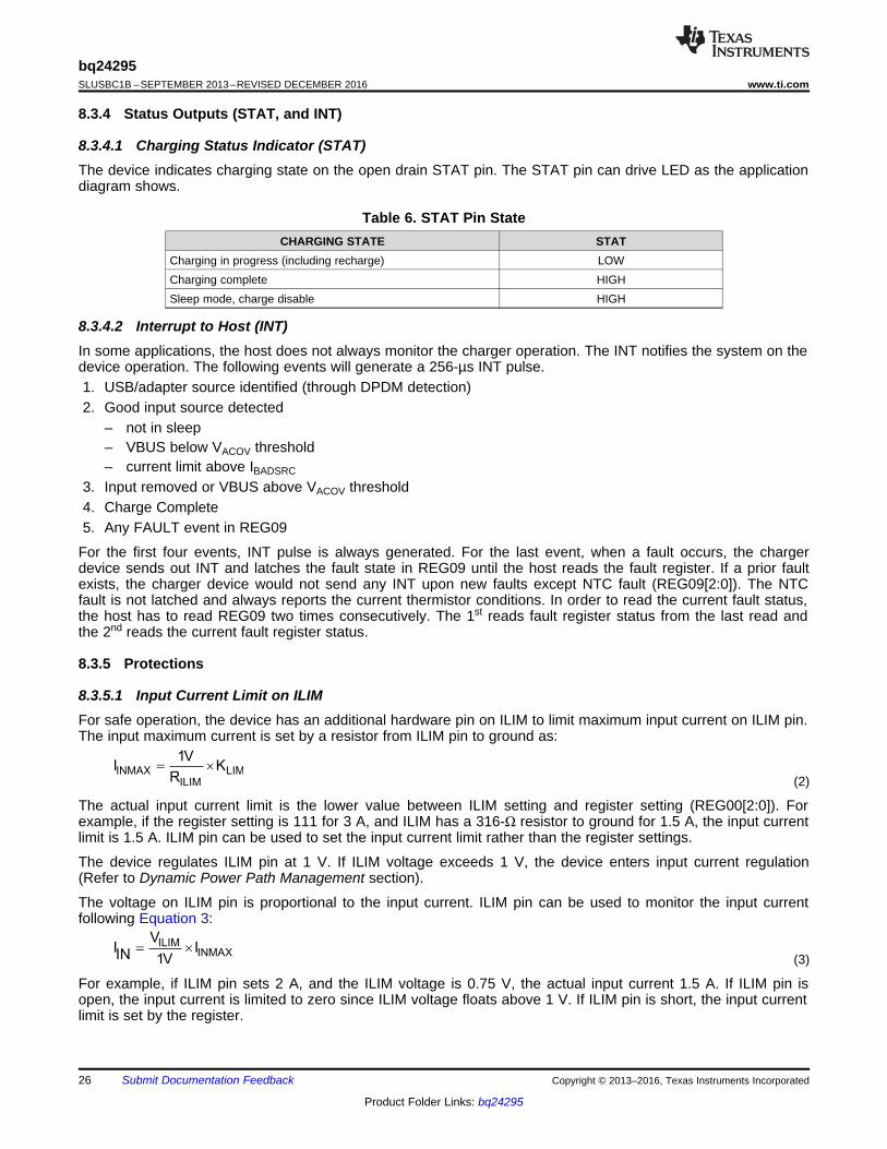
8.4 Device Functional Modes
8.4.1 Host Mode and Default ModeThe device is a host controlled device, but it can operate in default mode without host management. In defaultmode, the device can be used as an autonomous charger with no host or with host in sleep.
When the charger is in default mode, REG09[7] is HIGH. When the charger is in host mode, REG09[7] is LOW.After power-on-reset, the device starts in watchdog timer expiration state, or default mode. All the registers are inthe default settings. The device keeps charging the battery by default with 12-hour fast charging safety timer. Atthe end of the 12 hours, the charging is stopped and the buck converter continues to operate to supply systemload.
PORwatchdog timer expired
Reset registers
I2C interface enabled
I2C Write?Host Mode
Start watchdog timer
Host programs registers
Y
N
Default ModeReset watchdog timer
Reset registersReset REG01
bit[6]?
Y
N
Watchdog Timer
Expired?
I2C Write?
Y N
YN
28
bq24295SLUSBC1B –SEPTEMBER 2013–REVISED DECEMBER 2016 www.ti.com
Product Folder Links: bq24295
Submit Documentation Feedback Copyright © 2013–2016, Texas Instruments Incorporated
Device Functional Modes (continued)Any write command to device transitions the device from default mode to host mode. All the device parameterscan be programmed by the host. To keep the device in host mode, the host has to reset the watchdog timer bywriting 1 to REG01[6] before the watchdog timer expires (REG05[5:4]), or disable watchdog timer by settingREG05[5:4] = 00.
When the host changes watchdog timer configuration (REG05[5:4]), it is recommended to first disable watchdogby writing 00 to REG05[5:4] and then change the watchdog to new timer values. This ensures the watchdogtimer is restarted after new value is written.
Figure 20. Watchdog Timer Flow Chart
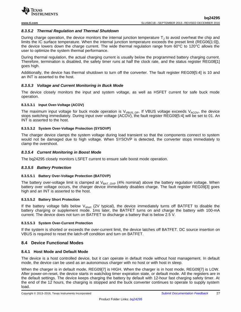
8.5 Programming
8.5.1 Serial InterfaceThe device uses I2C compatible interface for flexible charging parameter programming and instantaneous devicestatus reporting. I2C is a bi-directional 2-wire serial interface developed by Philips Semiconductor (now NXPSemiconductors). Only two bus lines are required: a serial data line (SDA) and a serial clock line (SCL). Devicescan be considered as masters or slaves when performing data transfers. A master is the device which initiates adata transfer on the bus and generates the clock signals to permit that transfer. At that time, any deviceaddressed is considered a slave.
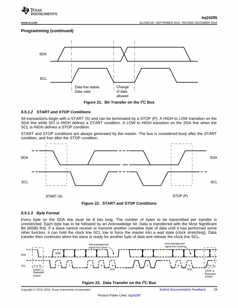
The device operates as a slave device with address 6BH, receiving control inputs from the master device likemicro controller or a digital signal processor. The I2C interface supports both standard mode (up to 100 kbits),and fast mode (up to 400 kbits).
Both SDA and SCL are bi-directional lines, connecting to the positive supply voltage via a current source or pull-up resistor. When the bus is free, both lines are HIGH. The SDA and SCL pins are open drain.
8.5.1.1 Data ValidityThe data on the SDA line must be stable during the HIGH period of the clock. The HIGH or LOW state of thedata line can only change when the clock signal on the SCL line is LOW. One clock pulse is generated for eachdata bit transferred.
SCL
SDA
START orRepeated
START
S or Sr 1 2 7 8 9
MSB
ACK
Acknowledgement
signal from slave
1 2 8 9
ACK
Acknowledgement
signal from receiver
STOP or
Repeated
START
P or Sr
START (S) STOP (P)
SDA
SCL
SDA
SCL
SDA
SCL
Data line stable;
Data valid
Change
of data
allowed
29
bq24295www.ti.com SLUSBC1B –SEPTEMBER 2013–REVISED DECEMBER 2016
Product Folder Links: bq24295
Submit Documentation FeedbackCopyright © 2013–2016, Texas Instruments Incorporated
Programming (continued)
Figure 21. Bit Transfer on the I2C Bus
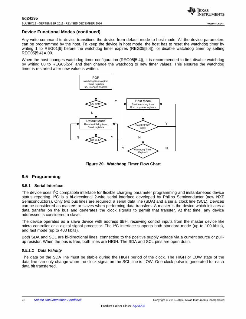
8.5.1.2 START and STOP ConditionsAll transactions begin with a START (S) and can be terminated by a STOP (P). A HIGH to LOW transition on theSDA line while SCl is HIGH defines a START condition. A LOW to HIGH transition on the SDA line when theSCL is HIGH defines a STOP condition.
START and STOP conditions are always generated by the master. The bus is considered busy after the STARTcondition, and free after the STOP condition.
Figure 22. START and STOP Conditions
8.5.1.3 Byte FormatEvery byte on the SDA line must be 8 bits long. The number of bytes to be transmitted per transfer isunrestricted. Each byte has to be followed by an Acknowledge bit. Data is transferred with the Most SignificantBit (MSB) first. If a slave cannot receive or transmit another complete byte of data until it has performed someother function, it can hold the clock line SCL low to force the master into a wait state (clock stretching). Datatransfer then continues when the slave is ready for another byte of data and release the clock line SCL.
Figure 23. Data Transfer on the I2C Bus
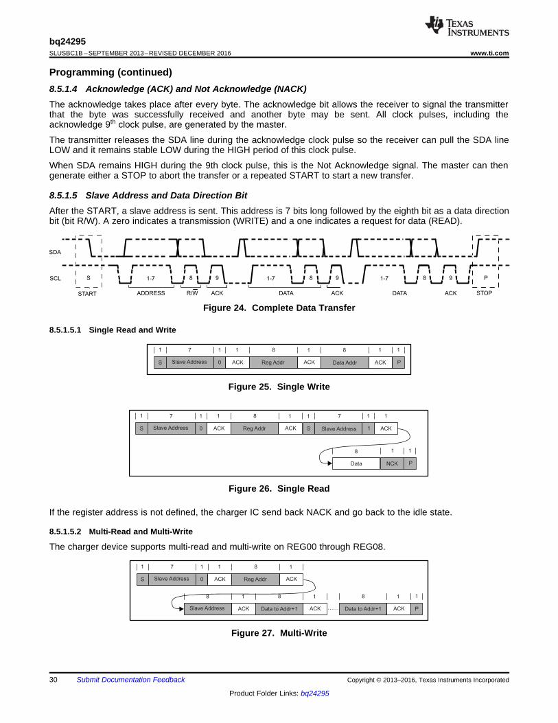
1 7
Slave AddressS
1 1
ACK
8
Reg Addr ACK
1
0
8
Slave Address
1
ACK
8
Data to Addr+1 ACK
1 8
Data to Addr+1 ACK
1
P
1
1 7
Slave AddressS
1 1
ACK
8
Reg Addr ACK
1
ACK
1
1
P
7
0 1
Data NCK
8
Slave Address
1
1
1
S
1 7
Slave AddressS
1 1
ACK
8
Reg Addr ACK
1
Data Addr ACK
1 1
P
8
0
START
SCL
SDA
S 1-7 8 9
ACK
1-7 8 9
ACK
1-7 8 9
STOP
P
ADDRESS R/W DATA ACKDATA
30
bq24295SLUSBC1B –SEPTEMBER 2013–REVISED DECEMBER 2016 www.ti.com
Product Folder Links: bq24295
Submit Documentation Feedback Copyright © 2013–2016, Texas Instruments Incorporated
Programming (continued)8.5.1.4 Acknowledge (ACK) and Not Acknowledge (NACK)The acknowledge takes place after every byte. The acknowledge bit allows the receiver to signal the transmitterthat the byte was successfully received and another byte may be sent. All clock pulses, including theacknowledge 9th clock pulse, are generated by the master.
The transmitter releases the SDA line during the acknowledge clock pulse so the receiver can pull the SDA lineLOW and it remains stable LOW during the HIGH period of this clock pulse.
When SDA remains HIGH during the 9th clock pulse, this is the Not Acknowledge signal. The master can thengenerate either a STOP to abort the transfer or a repeated START to start a new transfer.
8.5.1.5 Slave Address and Data Direction BitAfter the START, a slave address is sent. This address is 7 bits long followed by the eighth bit as a data directionbit (bit R/W). A zero indicates a transmission (WRITE) and a one indicates a request for data (READ).
Figure 24. Complete Data Transfer
8.5.1.5.1 Single Read and Write
Figure 25. Single Write
Figure 26. Single Read
If the register address is not defined, the charger IC send back NACK and go back to the idle state.
8.5.1.5.2 Multi-Read and Multi-Write
The charger device supports multi-read and multi-write on REG00 through REG08.
Figure 27. Multi-Write
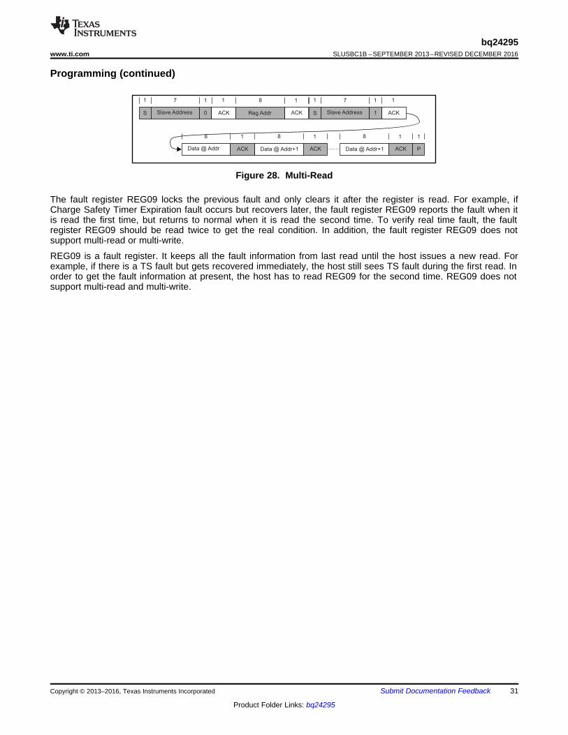
1 7
Slave AddressS
1 1
ACK
8
Reg Addr ACK
1
0
1 7
Slave AddressS
1 1
ACK1
8
Data @ Addr
1
ACK
8
Data @ Addr+1 ACK
1 8
Data @ Addr+1 ACK
1
P
1
31
bq24295www.ti.com SLUSBC1B –SEPTEMBER 2013–REVISED DECEMBER 2016
Product Folder Links: bq24295
Submit Documentation FeedbackCopyright © 2013–2016, Texas Instruments Incorporated
Programming (continued)
Figure 28. Multi-Read
The fault register REG09 locks the previous fault and only clears it after the register is read. For example, ifCharge Safety Timer Expiration fault occurs but recovers later, the fault register REG09 reports the fault when itis read the first time, but returns to normal when it is read the second time. To verify real time fault, the faultregister REG09 should be read twice to get the real condition. In addition, the fault register REG09 does notsupport multi-read or multi-write.
REG09 is a fault register. It keeps all the fault information from last read until the host issues a new read. Forexample, if there is a TS fault but gets recovered immediately, the host still sees TS fault during the first read. Inorder to get the fault information at present, the host has to read REG09 for the second time. REG09 does notsupport multi-read and multi-write.
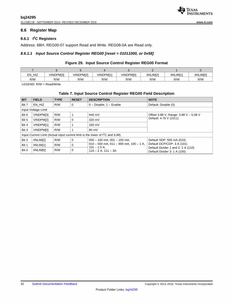
32
bq24295SLUSBC1B –SEPTEMBER 2013–REVISED DECEMBER 2016 www.ti.com
Product Folder Links: bq24295
Submit Documentation Feedback Copyright © 2013–2016, Texas Instruments Incorporated
8.6 Register Map
8.6.1 I2C RegistersAddress: 6BH. REG00-07 support Read and Write. REG08-0A are Read only.
8.6.1.1 Input Source Control Register REG00 [reset = 01011000, or 0x58]
Figure 29. Input Source Control Register REG00 Format
7 6 5 4 3 2 1 0EN_HIZ VINDPM[3] VINDPM[2] VINDPM[1] VINDPM[0] IINLIM[2] IINLIM[1] IINLIM[0]
R/W R/W R/W R/W R/W R/W R/W R/WLEGEND: R/W = Read/Write
Table 7. Input Source Control Register REG00 Field DescriptionBIT FIELD TYPE RESET DESCRIPTION NOTEBit 7 EN_HIZ R/W 0 0 – Disable, 1 – Enable Default: Disable (0)Input Voltage LimitBit 6 VINDPM[3] R/W 1 640 mV Offset 3.88 V, Range: 3.88 V – 5.08 V
Default: 4.76 V (1011)Bit 5 VINDPM[2] R/W 0 320 mVBit 4 VINDPM[1] R/W 1 160 mVBit 3 VINDPM[0] R/W 1 80 mVInput Current Limit (Actual input current limit is the lower of I2C and ILIM)Bit 2 IINLIM[2] R/W 0 000 – 100 mA, 001 – 150 mA,
010 – 500 mA, 011 – 900 mA, 100 – 1 A,101 – 1.5 A,110 – 2 A, 111 – 3A
Default SDP: 500 mA (010)Default DCP/CDP: 3 A (101)Default Divider 1 and 2: 2 A (110)Default Divider 3: 1 A (100)
Bit 1 IINLIM[1] R/W 0Bit 0 IINLIM[0] R/W 0
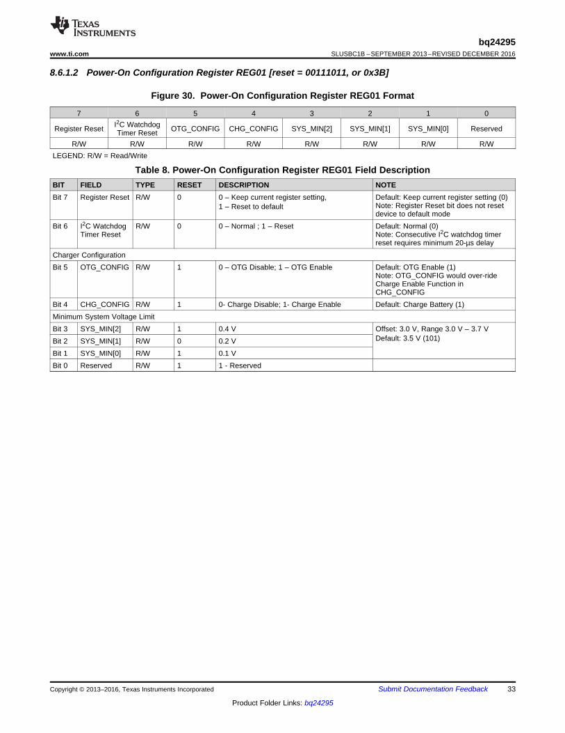
33
bq24295www.ti.com SLUSBC1B –SEPTEMBER 2013–REVISED DECEMBER 2016
Product Folder Links: bq24295
Submit Documentation FeedbackCopyright © 2013–2016, Texas Instruments Incorporated
8.6.1.2 Power-On Configuration Register REG01 [reset = 00111011, or 0x3B]
Figure 30. Power-On Configuration Register REG01 Format
7 6 5 4 3 2 1 0
Register Reset I2C WatchdogTimer Reset OTG_CONFIG CHG_CONFIG SYS_MIN[2] SYS_MIN[1] SYS_MIN[0] Reserved
R/W R/W R/W R/W R/W R/W R/W R/WLEGEND: R/W = Read/Write
Table 8. Power-On Configuration Register REG01 Field DescriptionBIT FIELD TYPE RESET DESCRIPTION NOTEBit 7 Register Reset R/W 0 0 – Keep current register setting,
1 – Reset to defaultDefault: Keep current register setting (0)Note: Register Reset bit does not resetdevice to default mode
Bit 6 I2C WatchdogTimer Reset
R/W 0 0 – Normal ; 1 – Reset Default: Normal (0)Note: Consecutive I2C watchdog timerreset requires minimum 20-µs delay
Charger ConfigurationBit 5 OTG_CONFIG R/W 1 0 – OTG Disable; 1 – OTG Enable Default: OTG Enable (1)
Note: OTG_CONFIG would over-rideCharge Enable Function inCHG_CONFIG
Bit 4 CHG_CONFIG R/W 1 0- Charge Disable; 1- Charge Enable Default: Charge Battery (1)Minimum System Voltage LimitBit 3 SYS_MIN[2] R/W 1 0.4 V Offset: 3.0 V, Range 3.0 V – 3.7 V
Default: 3.5 V (101)Bit 2 SYS_MIN[1] R/W 0 0.2 VBit 1 SYS_MIN[0] R/W 1 0.1 VBit 0 Reserved R/W 1 1 - Reserved
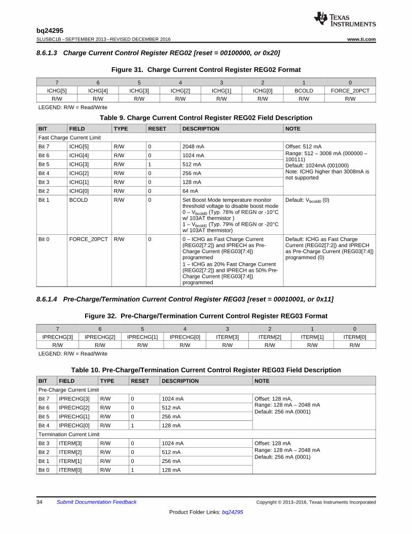
34
bq24295SLUSBC1B –SEPTEMBER 2013–REVISED DECEMBER 2016 www.ti.com
Product Folder Links: bq24295
Submit Documentation Feedback Copyright © 2013–2016, Texas Instruments Incorporated
8.6.1.3 Charge Current Control Register REG02 [reset = 00100000, or 0x20]
Figure 31. Charge Current Control Register REG02 Format
7 6 5 4 3 2 1 0ICHG[5] ICHG[4] ICHG[3] ICHG[2] ICHG[1] ICHG[0] BCOLD FORCE_20PCT
R/W R/W R/W R/W R/W R/W R/W R/WLEGEND: R/W = Read/Write
Table 9. Charge Current Control Register REG02 Field DescriptionBIT FIELD TYPE RESET DESCRIPTION NOTEFast Charge Current LimitBit 7 ICHG[5] R/W 0 2048 mA Offset: 512 mA
Range: 512 – 3008 mA (000000 –100111)Default: 1024mA (001000)Note: ICHG higher than 3008mA isnot supported
Bit 6 ICHG[4] R/W 0 1024 mABit 5 ICHG[3] R/W 1 512 mABit 4 ICHG[2] R/W 0 256 mABit 3 ICHG[1] R/W 0 128 mABit 2 ICHG[0] R/W 0 64 mABit 1 BCOLD R/W 0 Set Boost Mode temperature monitor
threshold voltage to disable boost mode0 – Vbcold0 (Typ. 76% of REGN or -10°Cw/ 103AT thermistor )1 – Vbcold1 (Typ. 79% of REGN or -20°Cw/ 103AT thermistor)
Default: Vbcold0 (0)
Bit 0 FORCE_20PCT R/W 0 0 – ICHG as Fast Charge Current(REG02[7:2]) and IPRECH as Pre-Charge Current (REG03[7:4])programmed1 – ICHG as 20% Fast Charge Current(REG02[7:2]) and IPRECH as 50% Pre-Charge Current (REG03[7:4])programmed
Default: ICHG as Fast ChargeCurrent (REG02[7:2]) and IPRECHas Pre-Charge Current (REG03[7:4])programmed (0)
8.6.1.4 Pre-Charge/Termination Current Control Register REG03 [reset = 00010001, or 0x11]
Figure 32. Pre-Charge/Termination Current Control Register REG03 Format
7 6 5 4 3 2 1 0IPRECHG[3] IPRECHG[2] IPRECHG[1] IPRECHG[0] ITERM[3] ITERM[2] ITERM[1] ITERM[0]
R/W R/W R/W R/W R/W R/W R/W R/WLEGEND: R/W = Read/Write
Table 10. Pre-Charge/Termination Current Control Register REG03 Field DescriptionBIT FIELD TYPE RESET DESCRIPTION NOTEPre-Charge Current LimitBit 7 IPRECHG[3] R/W 0 1024 mA Offset: 128 mA,
Range: 128 mA – 2048 mADefault: 256 mA (0001)
Bit 6 IPRECHG[2] R/W 0 512 mABit 5 IPRECHG[1] R/W 0 256 mABit 4 IPRECHG[0] R/W 1 128 mATermination Current LimitBit 3 ITERM[3] R/W 0 1024 mA Offset: 128 mA
Range: 128 mA – 2048 mADefault: 256 mA (0001)
Bit 2 ITERM[2] R/W 0 512 mABit 1 ITERM[1] R/W 0 256 mABit 0 ITERM[0] R/W 1 128 mA
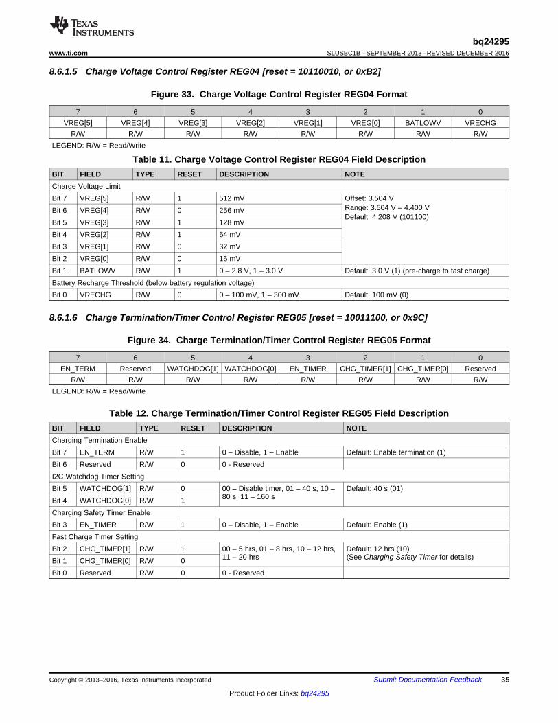
35
bq24295www.ti.com SLUSBC1B –SEPTEMBER 2013–REVISED DECEMBER 2016
Product Folder Links: bq24295
Submit Documentation FeedbackCopyright © 2013–2016, Texas Instruments Incorporated
8.6.1.5 Charge Voltage Control Register REG04 [reset = 10110010, or 0xB2]
Figure 33. Charge Voltage Control Register REG04 Format
7 6 5 4 3 2 1 0VREG[5] VREG[4] VREG[3] VREG[2] VREG[1] VREG[0] BATLOWV VRECHG
R/W R/W R/W R/W R/W R/W R/W R/WLEGEND: R/W = Read/Write
Table 11. Charge Voltage Control Register REG04 Field DescriptionBIT FIELD TYPE RESET DESCRIPTION NOTECharge Voltage LimitBit 7 VREG[5] R/W 1 512 mV Offset: 3.504 V
Range: 3.504 V – 4.400 VDefault: 4.208 V (101100)
Bit 6 VREG[4] R/W 0 256 mVBit 5 VREG[3] R/W 1 128 mVBit 4 VREG[2] R/W 1 64 mVBit 3 VREG[1] R/W 0 32 mVBit 2 VREG[0] R/W 0 16 mVBit 1 BATLOWV R/W 1 0 – 2.8 V, 1 – 3.0 V Default: 3.0 V (1) (pre-charge to fast charge)Battery Recharge Threshold (below battery regulation voltage)Bit 0 VRECHG R/W 0 0 – 100 mV, 1 – 300 mV Default: 100 mV (0)
8.6.1.6 Charge Termination/Timer Control Register REG05 [reset = 10011100, or 0x9C]
Figure 34. Charge Termination/Timer Control Register REG05 Format
7 6 5 4 3 2 1 0EN_TERM Reserved WATCHDOG[1] WATCHDOG[0] EN_TIMER CHG_TIMER[1] CHG_TIMER[0] Reserved
R/W R/W R/W R/W R/W R/W R/W R/WLEGEND: R/W = Read/Write
Table 12. Charge Termination/Timer Control Register REG05 Field DescriptionBIT FIELD TYPE RESET DESCRIPTION NOTECharging Termination EnableBit 7 EN_TERM R/W 1 0 – Disable, 1 – Enable Default: Enable termination (1)Bit 6 Reserved R/W 0 0 - ReservedI2C Watchdog Timer SettingBit 5 WATCHDOG[1] R/W 0 00 – Disable timer, 01 – 40 s, 10 –
80 s, 11 – 160 sDefault: 40 s (01)
Bit 4 WATCHDOG[0] R/W 1Charging Safety Timer EnableBit 3 EN_TIMER R/W 1 0 – Disable, 1 – Enable Default: Enable (1)Fast Charge Timer SettingBit 2 CHG_TIMER[1] R/W 1 00 – 5 hrs, 01 – 8 hrs, 10 – 12 hrs,
11 – 20 hrsDefault: 12 hrs (10)(See Charging Safety Timer for details)Bit 1 CHG_TIMER[0] R/W 0
Bit 0 Reserved R/W 0 0 - Reserved
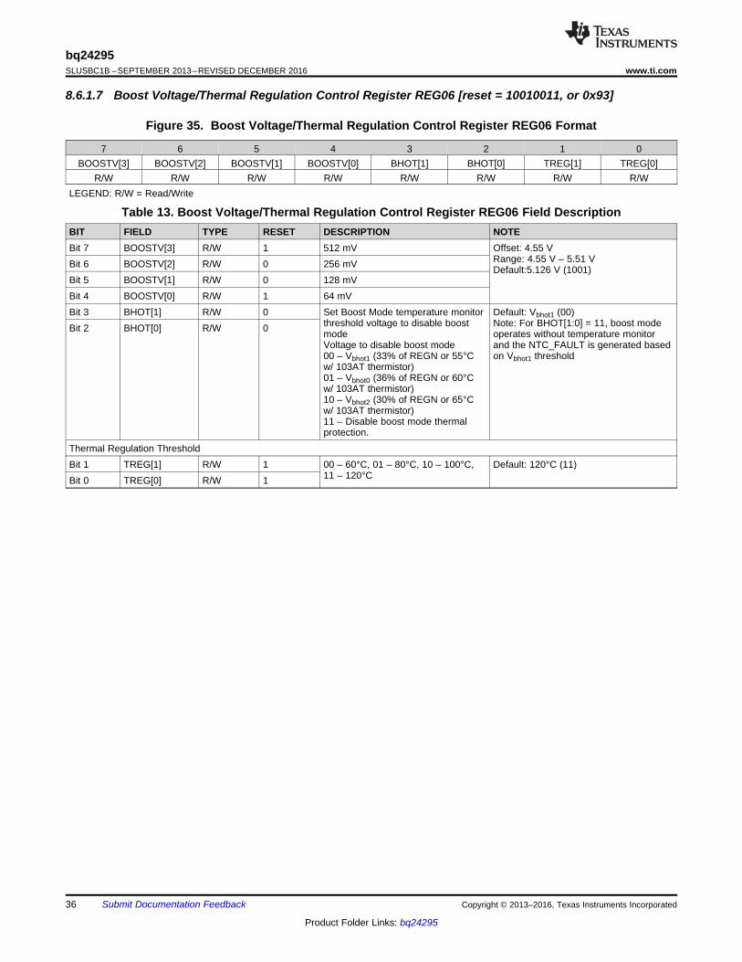
36
bq24295SLUSBC1B –SEPTEMBER 2013–REVISED DECEMBER 2016 www.ti.com
Product Folder Links: bq24295
Submit Documentation Feedback Copyright © 2013–2016, Texas Instruments Incorporated
8.6.1.7 Boost Voltage/Thermal Regulation Control Register REG06 [reset = 10010011, or 0x93]
Figure 35. Boost Voltage/Thermal Regulation Control Register REG06 Format
7 6 5 4 3 2 1 0BOOSTV[3] BOOSTV[2] BOOSTV[1] BOOSTV[0] BHOT[1] BHOT[0] TREG[1] TREG[0]
R/W R/W R/W R/W R/W R/W R/W R/WLEGEND: R/W = Read/Write
Table 13. Boost Voltage/Thermal Regulation Control Register REG06 Field DescriptionBIT FIELD TYPE RESET DESCRIPTION NOTEBit 7 BOOSTV[3] R/W 1 512 mV Offset: 4.55 V
Range: 4.55 V – 5.51 VDefault:5.126 V (1001)Bit 6 BOOSTV[2] R/W 0 256 mV
Bit 5 BOOSTV[1] R/W 0 128 mVBit 4 BOOSTV[0] R/W 1 64 mVBit 3 BHOT[1] R/W 0 Set Boost Mode temperature monitor
threshold voltage to disable boostmodeVoltage to disable boost mode00 – Vbhot1 (33% of REGN or 55°Cw/ 103AT thermistor)01 – Vbhot0 (36% of REGN or 60°Cw/ 103AT thermistor)10 – Vbhot2 (30% of REGN or 65°Cw/ 103AT thermistor)11 – Disable boost mode thermalprotection.
Default: Vbhot1 (00)Note: For BHOT[1:0] = 11, boost modeoperates without temperature monitorand the NTC_FAULT is generated basedon Vbhot1 threshold
Bit 2 BHOT[0] R/W 0
Thermal Regulation ThresholdBit 1 TREG[1] R/W 1 00 – 60°C, 01 – 80°C, 10 – 100°C,
11 – 120°CDefault: 120°C (11)
Bit 0 TREG[0] R/W 1
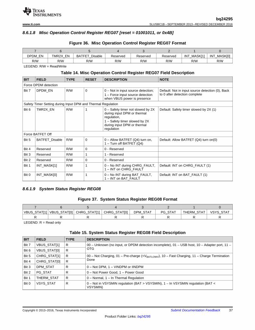
37
bq24295www.ti.com SLUSBC1B –SEPTEMBER 2013–REVISED DECEMBER 2016
Product Folder Links: bq24295
Submit Documentation FeedbackCopyright © 2013–2016, Texas Instruments Incorporated
8.6.1.8 Misc Operation Control Register REG07 [reset = 01001011, or 0x4B]
Figure 36. Misc Operation Control Register REG07 Format
7 6 5 4 3 2 1 0DPDM_EN TMR2X_EN BATFET_Disable Reserved Reserved Reserved INT_MASK[1] INT_MASK[0]
R/W R/W R/W R/W R/W R/W R/W R/WLEGEND: R/W = Read/Write
Table 14. Misc Operation Control Register REG07 Field DescriptionBIT FIELD TYPE RESET DESCRIPTION NOTEForce DPDM detectionBit 7 DPDM_EN R/W 0 0 – Not in input source detection;
1 – Force input source detectionwhen VBUS power is presence
Default: Not in input source detection (0), Backto 0 after detection complete
Safety Timer Setting during Input DPM and Thermal RegulationBit 6 TMR2X_EN R/W 1 0 – Safety timer not slowed by 2X
during input DPM or thermalregulation,1 – Safety timer slowed by 2Xduring input DPM or thermalregulation
Default: Safety timer slowed by 2X (1)
Force BATFET OffBit 5 BATFET_Disable R/W 0 0 – Allow BATFET (Q4) turn on,
1 – Turn off BATFET (Q4)Default: Allow BATFET (Q4) turn on(0)
Bit 4 Reserved R/W 0 0 - ReservedBit 3 Reserved R/W 1 1 - ReservedBit 2 Reserved R/W 0 0 - ReservedBit 1 INT_MASK[1] R/W 1 0 – No INT during CHRG_FAULT,
1 – INT on CHRG_FAULTDefault: INT on CHRG_FAULT (1)
Bit 0 INT_MASK[0] R/W 1 0 – No INT during BAT_FAULT,1 – INT on BAT_FAULT
Default: INT on BAT_FAULT (1)
8.6.1.9 System Status Register REG08
Figure 37. System Status Register REG08 Format
7 6 5 4 3 2 1 0VBUS_STAT[1] VBUS_STAT[0] CHRG_STAT[1] CHRG_STAT[0] DPM_STAT PG_STAT THERM_STAT VSYS_STAT
R R R R R R R RLEGEND: R = Read only
Table 15. System Status Register REG08 Field DescriptionBIT FIELD TYPE DESCRIPTIONBit 7 VBUS_STAT[1] R 00 – Unknown (no input, or DPDM detection incomplete), 01 – USB host, 10 – Adapter port, 11 –
OTGBit 6 VBUS_STAT[0] RBit 5 CHRG_STAT[1] R 00 – Not Charging, 01 – Pre-charge (<VBATLOWV), 10 – Fast Charging, 11 – Charge Termination
DoneBit 4 CHRG_STAT[0] RBit 3 DPM_STAT R 0 – Not DPM, 1 – VINDPM or IINDPMBit 2 PG_STAT R 0 – Not Power Good, 1 – Power GoodBit 1 THERM_STAT R 0 – Normal, 1 – In Thermal RegulationBit 0 VSYS_STAT R 0 – Not in VSYSMIN regulation (BAT > VSYSMIN), 1 – In VSYSMIN regulation (BAT <
VSYSMIN)
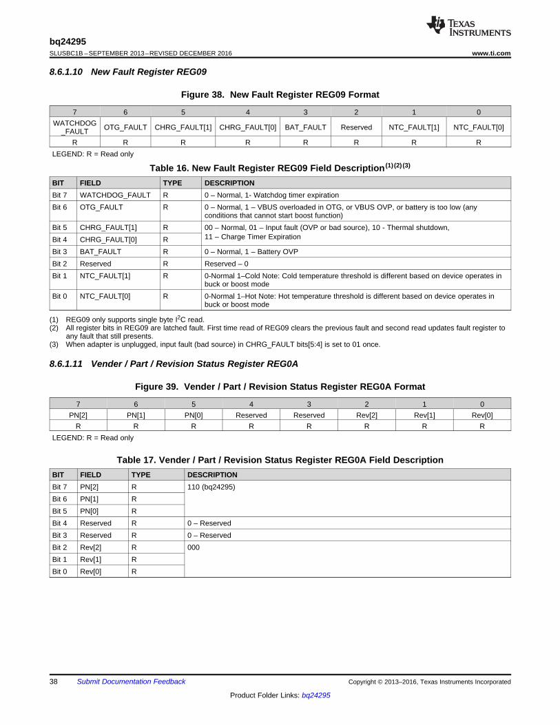
38
bq24295SLUSBC1B –SEPTEMBER 2013–REVISED DECEMBER 2016 www.ti.com
Product Folder Links: bq24295
Submit Documentation Feedback Copyright © 2013–2016, Texas Instruments Incorporated
8.6.1.10 New Fault Register REG09
Figure 38. New Fault Register REG09 Format
7 6 5 4 3 2 1 0WATCHDOG
_FAULT OTG_FAULT CHRG_FAULT[1] CHRG_FAULT[0] BAT_FAULT Reserved NTC_FAULT[1] NTC_FAULT[0]
R R R R R R R RLEGEND: R = Read only
(1) REG09 only supports single byte I2C read.(2) All register bits in REG09 are latched fault. First time read of REG09 clears the previous fault and second read updates fault register to
any fault that still presents.(3) When adapter is unplugged, input fault (bad source) in CHRG_FAULT bits[5:4] is set to 01 once.
Table 16. New Fault Register REG09 Field Description (1) (2) (3)
BIT FIELD TYPE DESCRIPTIONBit 7 WATCHDOG_FAULT R 0 – Normal, 1- Watchdog timer expirationBit 6 OTG_FAULT R 0 – Normal, 1 – VBUS overloaded in OTG, or VBUS OVP, or battery is too low (any
conditions that cannot start boost function)Bit 5 CHRG_FAULT[1] R 00 – Normal, 01 – Input fault (OVP or bad source), 10 - Thermal shutdown,
11 – Charge Timer ExpirationBit 4 CHRG_FAULT[0] RBit 3 BAT_FAULT R 0 – Normal, 1 – Battery OVPBit 2 Reserved R Reserved – 0Bit 1 NTC_FAULT[1] R 0-Normal 1–Cold Note: Cold temperature threshold is different based on device operates in
buck or boost modeBit 0 NTC_FAULT[0] R 0-Normal 1–Hot Note: Hot temperature threshold is different based on device operates in
buck or boost mode
8.6.1.11 Vender / Part / Revision Status Register REG0A
Figure 39. Vender / Part / Revision Status Register REG0A Format
7 6 5 4 3 2 1 0PN[2] PN[1] PN[0] Reserved Reserved Rev[2] Rev[1] Rev[0]
R R R R R R R RLEGEND: R = Read only
Table 17. Vender / Part / Revision Status Register REG0A Field DescriptionBIT FIELD TYPE DESCRIPTIONBit 7 PN[2] R 110 (bq24295)Bit 6 PN[1] RBit 5 PN[0] RBit 4 Reserved R 0 – ReservedBit 3 Reserved R 0 – ReservedBit 2 Rev[2] R 000Bit 1 Rev[1] RBit 0 Rev[0] R
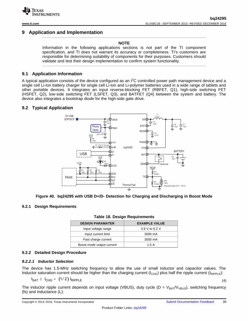
( )SAT CHG RIPPLEI I 1/ 2 I³ +
VBUS
PMID
OTG
D+
D–
STAT
SDA
SCL
INT
CE
SW
BTST
REGN
PGND
SYS
BAT
ILIM
TS
+3.3V
Host
REGN
SYS
USB
5V USB
bq24295
Phone
Tablet
BATTERY
C5
10 Fm
C1
C2
1 FmC3
47nF
C4
4.7 Fm
L1
2.2 Hm
SYS
SDP/DCP
Thermal Pad
R1 317W (1.5A max)
RTH
10kW
RT1
5.25kW
RT2
31.23kW
R2
2.2kW
R3
10kW
R4
10kW
R5
10kW
R6
10kW
C6
10 Fm
C7
10 Fm
20 F minm
QON Optional
Charge Enable (0°C - 45°C)
39
bq24295www.ti.com SLUSBC1B –SEPTEMBER 2013–REVISED DECEMBER 2016
Product Folder Links: bq24295
Submit Documentation FeedbackCopyright © 2013–2016, Texas Instruments Incorporated
9 Application and Implementation
NOTEInformation in the following applications sections is not part of the TI componentspecification, and TI does not warrant its accuracy or completeness. TI’s customers areresponsible for determining suitability of components for their purposes. Customers shouldvalidate and test their design implementation to confirm system functionality.
9.1 Application InformationA typical application consists of the device configured as an I2C controlled power path management device and asingle cell Li-Ion battery charger for single cell Li-Ion and Li-polymer batteries used in a wide range of tablets andother portable devices. It integrates an input reverse-blocking FET (RBFET, Q1), high-side switching FET(HSFET, Q2), low-side switching FET (LSFET, Q3), and BATFET (Q4) between the system and battery. Thedevice also integrates a bootstrap diode for the high-side gate drive.
9.2 Typical Application
Figure 40. bq24295 with USB D+/D- Detection for Charging and Discharging in Boost Mode
9.2.1 Design Requirements
Table 18. Design RequirementsDESIGN PARAMATER EXAMPLE VALUE
Input voltage range 3.9 V to 6.2 VInput current limit 3000 mA
Fast charge current 3000 mABoost mode output current 1.5 A
9.2.2 Detailed Design Procedure
9.2.2.1 Inductor SelectionThe device has 1.5-MHz switching frequency to allow the use of small inductor and capacitor values. TheInductor saturation current should be higher than the charging current (ICHG) plus half the ripple current (IRIPPLE):
(4)
The inductor ripple current depends on input voltage (VBUS), duty cycle (D = VBAT/VVBUS), switching frequency(fs) and inductance (L):
OUT OUTO 2
IN
V VV 1
V8LC s
æ öç ÷D = -ç ÷¦ è ø
RIPPLECOUT RIPPLE
II 0.29 I
2 3= » ´
´
CIN CHGI I D (1 D)= ´ ´ -
INRIPPLE
V D (1 D) I
s L
´ ´ -=
¦ ´
40
bq24295SLUSBC1B –SEPTEMBER 2013–REVISED DECEMBER 2016 www.ti.com
Product Folder Links: bq24295
Submit Documentation Feedback Copyright © 2013–2016, Texas Instruments Incorporated
(5)
The maximum inductor ripple current happens with D = 0.5 or close to 0.5. Usually inductor ripple is designed inthe range of (20 – 40%) maximum charging current as a trade-off between inductor size and efficiency for apractical design.
9.2.2.2 Input CapacitorInput capacitor should have enough ripple current rating to absorb input switching ripple current. The worst caseRMS ripple current is half of the charging current when duty cycle is 0.5. If the converter does not operate at50% duty cycle, then the worst case capacitor RMS current ICIN occurs where the duty cycle is closest to 50%and can be estimated by the following equation:
(6)
For best performance, VBUS should be decouple to PGND with 1-μF capacitance. The remaining input capacitorshould be place on PMID.
Low ESR ceramic capacitor such as X7R or X5R is preferred for input decoupling capacitor and should beplaced to the drain of the high side MOSFET and source of the low side MOSFET as close as possible. Voltagerating of the capacitor must be higher than normal input voltage level. 25-V rating or higher capacitor is preferredfor 15-V input voltage. 22-μF capacitance is suggested for typical of 3-A to 4-A charging current.
9.2.2.3 Output CapacitorOutput capacitor also should have enough ripple current rating to absorb output switching ripple current. Theoutput capacitor RMS current ICOUT is given:
(7)
The output capacitor voltage ripple can be calculated as follows:
(8)
At certain input/output voltage and switching frequency, the voltage ripple can be reduced by increasing theoutput filter LC.
The charger device has internal loop compensator. To get good loop stability, the resonant frequency of theoutput inductor and output capacitor should be designed between 15 kHz and 36 kHz. The preferred ceramiccapacitor is 6 V or higher rating, X7R or X5R.
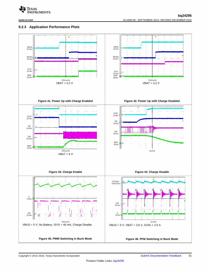
4 s/divm
IL1A/div
SW2V/div
SYS3p7100mV/div
400ns/div
SW
2V/div
IL
1A/div
STAT
2V/div
CE
2V/div
SW
5V/div
IBAT
1A/div
200 s/divm
STAT
2V/div
CE
5V/div
SW
5V/div
IBAT
1A/div
4 s/divm
IBAT
2A/div
100ms/div
SYS
2V/div
REGN
5V/div
VBUS
5V/div
VBUS
5V/div
REGN
5V/div
SYS
2V/div
IBAT
2A/div
100ms/div
41
bq24295www.ti.com SLUSBC1B –SEPTEMBER 2013–REVISED DECEMBER 2016
Product Folder Links: bq24295
Submit Documentation FeedbackCopyright © 2013–2016, Texas Instruments Incorporated
9.2.3 Application Performance Plots
VBAT = 3.2 V
Figure 41. Power Up with Charge Enabled
VBAT = 3.2 V
Figure 42. Power Up with Charge Disabled
VBAT = 5 V
Figure 43. Charge Enable Figure 44. Charge Disable
VBUS = 5 V, No Battery, ISYS = 40 mA, Charge Disable
Figure 45. PWM Switching in Buck Mode
VBUS = 5 V, VBAT = 3.6 V, ICHG = 2.5 A
Figure 46. PFM Switching in Buck Mode
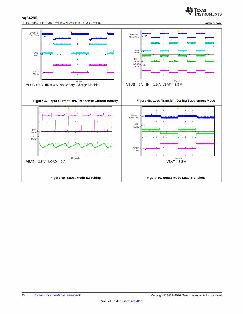
400ns/div
IL
1A/div
SW
2V/div
4ms/div
IVBUS
1A/div
IBAT
1A/div
VBUS
200mV/div
2ms/div
IVBUS2A/div
ISYS2A/div
SYS3p5500mV/div
20ms/div
IVBUS2A/div
IBAT2A/div
ISYS2A/div
SYS3p8500mV/div
42
bq24295SLUSBC1B –SEPTEMBER 2013–REVISED DECEMBER 2016 www.ti.com
Product Folder Links: bq24295
Submit Documentation Feedback Copyright © 2013–2016, Texas Instruments Incorporated
VBUS = 5 V, IIN = 3 A, No Battery, Charge Disable
Figure 47. Input Current DPM Response without Battery
VBUS = 5 V, IIN = 1.5 A, VBAT = 3.8 V
Figure 48. Load Transient During Supplement Mode
VBAT = 3.8 V, ILOAD = 1 A
Figure 49. Boost Mode Switching
VBAT = 3.8 V
Figure 50. Boost Mode Load Transient
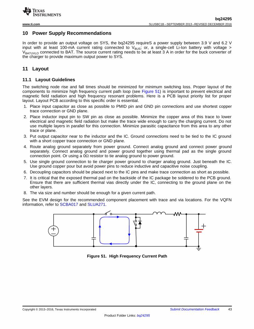
43
bq24295www.ti.com SLUSBC1B –SEPTEMBER 2013–REVISED DECEMBER 2016
Product Folder Links: bq24295
Submit Documentation FeedbackCopyright © 2013–2016, Texas Instruments Incorporated
10 Power Supply Recommendations
In order to provide an output voltage on SYS, the bq24295 requireS a power supply between 3.9 V and 6.2 Vinput with at least 100-mA current rating connected to VBUS; or, a single-cell Li-Ion battery with voltage >VBATUVLO connected to BAT. The source current rating needs to be at least 3 A in order for the buck converter ofthe charger to provide maximum output power to SYS.
11 Layout
11.1 Layout GuidelinesThe switching node rise and fall times should be minimized for minimum switching loss. Proper layout of thecomponents to minimize high frequency current path loop (see Figure 51) is important to prevent electrical andmagnetic field radiation and high frequency resonant problems. Here is a PCB layout priority list for properlayout. Layout PCB according to this specific order is essential.1. Place input capacitor as close as possible to PMID pin and GND pin connections and use shortest copper
trace connection or GND plane.2. Place inductor input pin to SW pin as close as possible. Minimize the copper area of this trace to lower
electrical and magnetic field radiation but make the trace wide enough to carry the charging current. Do notuse multiple layers in parallel for this connection. Minimize parasitic capacitance from this area to any othertrace or plane.
3. Put output capacitor near to the inductor and the IC. Ground connections need to be tied to the IC groundwith a short copper trace connection or GND plane.
4. Route analog ground separately from power ground. Connect analog ground and connect power groundseparately. Connect analog ground and power ground together using thermal pad as the single groundconnection point. Or using a 0Ω resistor to tie analog ground to power ground.
5. Use single ground connection to tie charger power ground to charger analog ground. Just beneath the IC.Use ground copper pour but avoid power pins to reduce inductive and capacitive noise coupling.
6. Decoupling capacitors should be placed next to the IC pins and make trace connection as short as possible.7. It is critical that the exposed thermal pad on the backside of the IC package be soldered to the PCB ground.
Ensure that there are sufficient thermal vias directly under the IC, connecting to the ground plane on theother layers.
8. The via size and number should be enough for a given current path.
See the EVM design for the recommended component placement with trace and via locations. For the VQFNinformation, refer to SCBA017 and SLUA271.
Figure 51. High Frequency Current Path
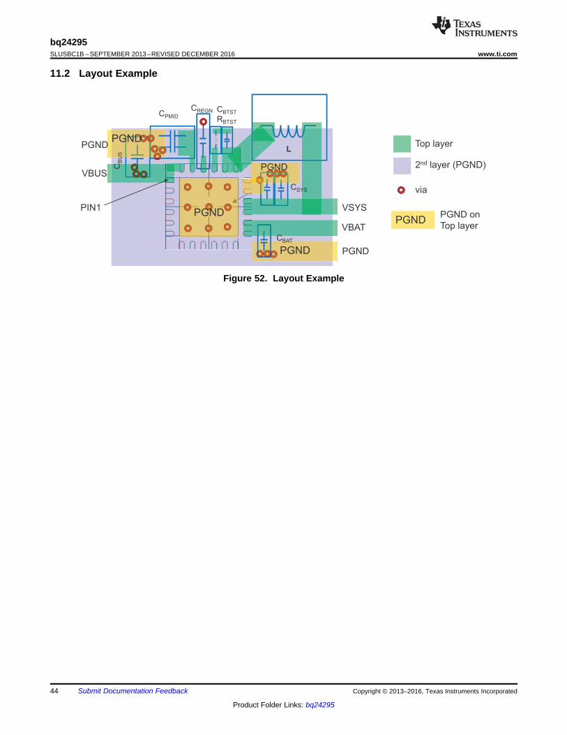
Top layer
2nd layer (PGND)
via
CPMID
CREGN
L
PGND
CBTST
RBTST
PGND
PGNDPGND on
Top layer
VSYS
VBAT
PGND
PGND
VBUS
PIN1PGND
CB
US
CBAT
CSYS
PGND
44
bq24295SLUSBC1B –SEPTEMBER 2013–REVISED DECEMBER 2016 www.ti.com
Product Folder Links: bq24295
Submit Documentation Feedback Copyright © 2013–2016, Texas Instruments Incorporated
11.2 Layout Example
Figure 52. Layout Example
45
bq24295www.ti.com SLUSBC1B –SEPTEMBER 2013–REVISED DECEMBER 2016
Product Folder Links: bq24295
Submit Documentation FeedbackCopyright © 2013–2016, Texas Instruments Incorporated
12 Device and Documentation Support
12.1 Documentation Support
12.1.1 Related Documentationbq24296/7 EVM (PWR021) User’s Guide (SLUUAQ1)
Quad Flatpack No-Lead Logic Packages Application Report (SCBA017)
QFN/SON PCB Attachment Application Report (SLUA271)
12.2 Receiving Notification of Documentation UpdatesTo receive notification of documentation updates, navigate to the device product folder on ti.com. In the upperright corner, click on Alert me to register and receive a weekly digest of any product information that haschanged. For change details, review the revision history included in any revised document.
12.3 Community ResourcesThe following links connect to TI community resources. Linked contents are provided "AS IS" by the respectivecontributors. They do not constitute TI specifications and do not necessarily reflect TI's views; see TI's Terms ofUse.
TI E2E™ Online Community TI's Engineer-to-Engineer (E2E) Community. Created to foster collaborationamong engineers. At e2e.ti.com, you can ask questions, share knowledge, explore ideas and helpsolve problems with fellow engineers.
Design Support TI's Design Support Quickly find helpful E2E forums along with design support tools andcontact information for technical support.
12.4 TrademarksE2E is a trademark of Texas Instruments.All other trademarks are the property of their respective owners.
12.5 Electrostatic Discharge CautionThese devices have limited built-in ESD protection. The leads should be shorted together or the device placed in conductive foamduring storage or handling to prevent electrostatic damage to the MOS gates.
12.6 GlossarySLYZ022 — TI Glossary.
This glossary lists and explains terms, acronyms, and definitions.
13 Mechanical, Packaging, and Orderable InformationThe following pages include mechanical packaging and orderable information. This information is the mostcurrent data available for the designated devices. This data is subject to change without notice and revision ofthis document. For browser-based versions of this data sheet, refer to the left-hand navigation.
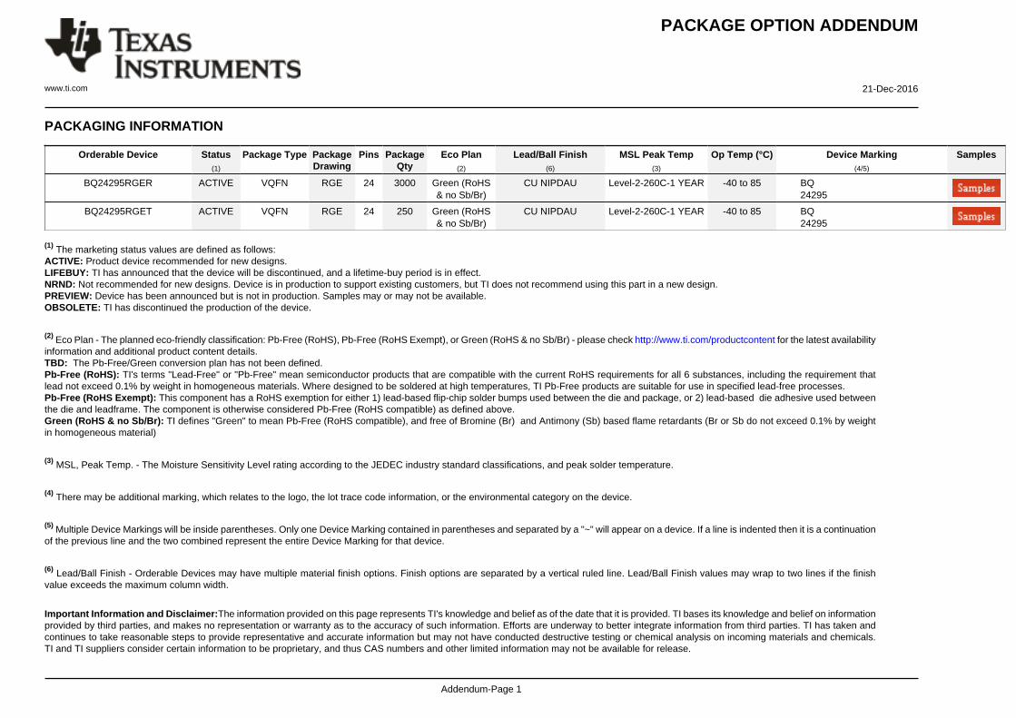
PACKAGE OPTION ADDENDUM
www.ti.com 21-Dec-2016
Addendum-Page 1
PACKAGING INFORMATION
Orderable Device Status(1)
Package Type PackageDrawing
Pins PackageQty
Eco Plan(2)
Lead/Ball Finish(6)
MSL Peak Temp(3)
Op Temp (°C) Device Marking(4/5)
Samples
BQ24295RGER ACTIVE VQFN RGE 24 3000 Green (RoHS& no Sb/Br)
CU NIPDAU Level-2-260C-1 YEAR -40 to 85 BQ24295
BQ24295RGET ACTIVE VQFN RGE 24 250 Green (RoHS& no Sb/Br)
CU NIPDAU Level-2-260C-1 YEAR -40 to 85 BQ24295
(1) The marketing status values are defined as follows:ACTIVE: Product device recommended for new designs.LIFEBUY: TI has announced that the device will be discontinued, and a lifetime-buy period is in effect.NRND: Not recommended for new designs. Device is in production to support existing customers, but TI does not recommend using this part in a new design.PREVIEW: Device has been announced but is not in production. Samples may or may not be available.OBSOLETE: TI has discontinued the production of the device.
(2) Eco Plan - The planned eco-friendly classification: Pb-Free (RoHS), Pb-Free (RoHS Exempt), or Green (RoHS & no Sb/Br) - please check http://www.ti.com/productcontent for the latest availabilityinformation and additional product content details.TBD: The Pb-Free/Green conversion plan has not been defined.Pb-Free (RoHS): TI's terms "Lead-Free" or "Pb-Free" mean semiconductor products that are compatible with the current RoHS requirements for all 6 substances, including the requirement thatlead not exceed 0.1% by weight in homogeneous materials. Where designed to be soldered at high temperatures, TI Pb-Free products are suitable for use in specified lead-free processes.Pb-Free (RoHS Exempt): This component has a RoHS exemption for either 1) lead-based flip-chip solder bumps used between the die and package, or 2) lead-based die adhesive used betweenthe die and leadframe. The component is otherwise considered Pb-Free (RoHS compatible) as defined above.Green (RoHS & no Sb/Br): TI defines "Green" to mean Pb-Free (RoHS compatible), and free of Bromine (Br) and Antimony (Sb) based flame retardants (Br or Sb do not exceed 0.1% by weightin homogeneous material)
(3) MSL, Peak Temp. - The Moisture Sensitivity Level rating according to the JEDEC industry standard classifications, and peak solder temperature.
(4) There may be additional marking, which relates to the logo, the lot trace code information, or the environmental category on the device.
(5) Multiple Device Markings will be inside parentheses. Only one Device Marking contained in parentheses and separated by a "~" will appear on a device. If a line is indented then it is a continuationof the previous line and the two combined represent the entire Device Marking for that device.
(6) Lead/Ball Finish - Orderable Devices may have multiple material finish options. Finish options are separated by a vertical ruled line. Lead/Ball Finish values may wrap to two lines if the finishvalue exceeds the maximum column width.
Important Information and Disclaimer:The information provided on this page represents TI's knowledge and belief as of the date that it is provided. TI bases its knowledge and belief on informationprovided by third parties, and makes no representation or warranty as to the accuracy of such information. Efforts are underway to better integrate information from third parties. TI has taken andcontinues to take reasonable steps to provide representative and accurate information but may not have conducted destructive testing or chemical analysis on incoming materials and chemicals.TI and TI suppliers consider certain information to be proprietary, and thus CAS numbers and other limited information may not be available for release.
PACKAGE OPTION ADDENDUM
www.ti.com 21-Dec-2016
Addendum-Page 2
In no event shall TI's liability arising out of such information exceed the total purchase price of the TI part(s) at issue in this document sold by TI to Customer on an annual basis.
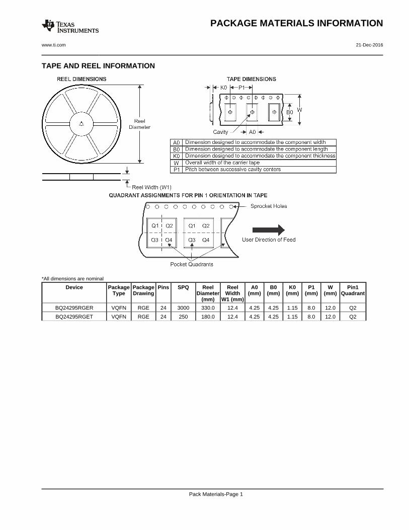
TAPE AND REEL INFORMATION
*All dimensions are nominal
Device PackageType
PackageDrawing
Pins SPQ ReelDiameter
(mm)
ReelWidth
W1 (mm)
A0(mm)
B0(mm)
K0(mm)
P1(mm)
W(mm)
Pin1Quadrant
BQ24295RGER VQFN RGE 24 3000 330.0 12.4 4.25 4.25 1.15 8.0 12.0 Q2
BQ24295RGET VQFN RGE 24 250 180.0 12.4 4.25 4.25 1.15 8.0 12.0 Q2
PACKAGE MATERIALS INFORMATION
www.ti.com 21-Dec-2016
Pack Materials-Page 1
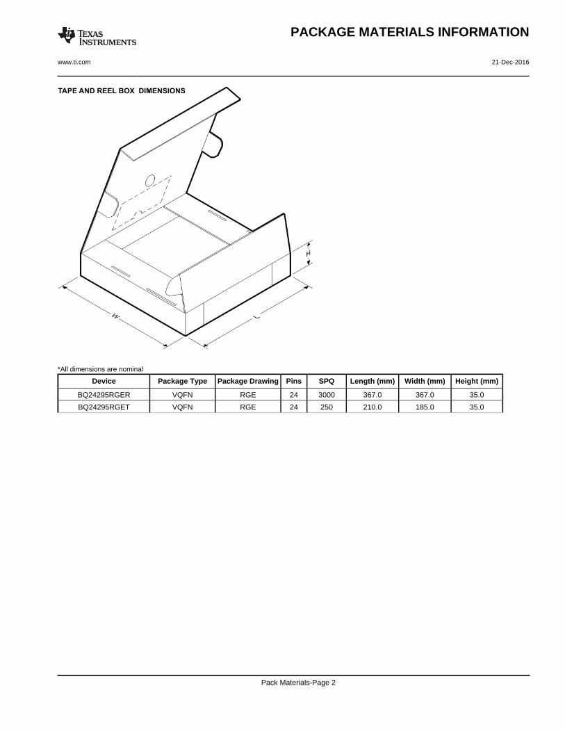
*All dimensions are nominal
Device Package Type Package Drawing Pins SPQ Length (mm) Width (mm) Height (mm)
BQ24295RGER VQFN RGE 24 3000 367.0 367.0 35.0
BQ24295RGET VQFN RGE 24 250 210.0 185.0 35.0
PACKAGE MATERIALS INFORMATION
www.ti.com 21-Dec-2016
Pack Materials-Page 2
GENERIC PACKAGE VIEW
Images above are just a representation of the package family, actual package may vary.Refer to the product data sheet for package details.
RGE 24 VQFN - 1 mm max heightPLASTIC QUAD FLATPACK - NO LEAD
4204104/H
NOTES:
1. All linear dimensions are in millimeters. Any dimensions in parenthesis are for reference only. Dimensioning and tolerancing
per ASME Y14.5M.
2. This drawing is subject to change without notice.
3. The package thermal pad must be soldered to the printed circuit board for thermal and mechanical performance.
PACKAGE OUTLINE
www.ti.com
4219016 / A 08/2017
VQFN - 1 mm max height
PLASTIC QUAD FLATPACK- NO LEAD
RGE0024H
A
0.08 C
0.1 C A B
0.05 C
B
SYMM
SYMM
4.1
3.9
4.1
3.9
PIN 1 INDEX AREA
1 MAX
0.05
0.00
SEATING PLANE
C
2X 2.5
2.7±0.1
2X
2.5
20X 0.5
1
6
7
12
13
18
19
24
24X
0.30
0.18
24X
0.48
0.28
(0.2) TYP
PIN 1 ID
(OPTIONAL)
25
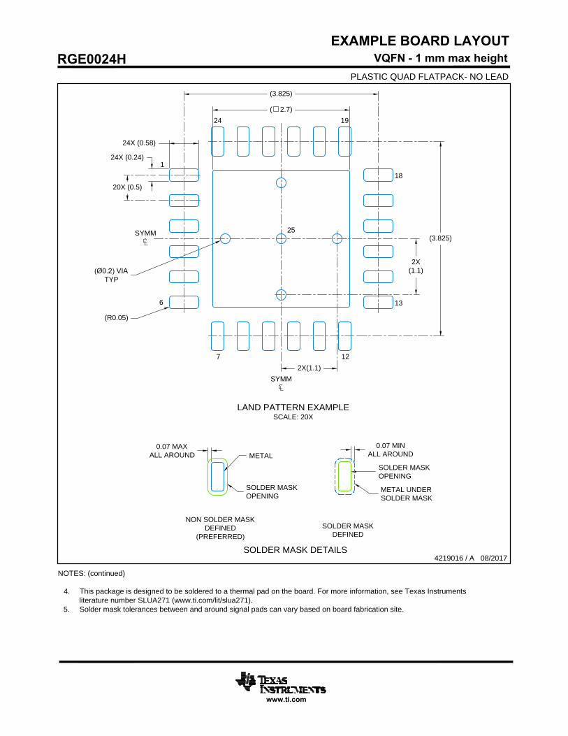
NOTES: (continued)
4. This package is designed to be soldered to a thermal pad on the board. For more information, see Texas Instruments
literature number SLUA271 (www.ti.com/lit/slua271).5. Solder mask tolerances between and around signal pads can vary based on board fabrication site.
EXAMPLE BOARD LAYOUT
4219016 / A 08/2017
www.ti.com
VQFN - 1 mm max height
RGE0024H
PLASTIC QUAD FLATPACK- NO LEAD
SYMM
SYMM
LAND PATTERN EXAMPLE
SCALE: 20X
2X
(1.1)
2X(1.1)
(3.825)
(3.825)
( 2.7)
1
6
7 12
13
18
1924
25
24X (0.58)
24X (0.24)
20X (0.5)
(R0.05)
(Ø0.2) VIA
TYP
SOLDER MASK DETAILS
NON SOLDER MASK
DEFINED
(PREFERRED)
SOLDER MASK
DEFINED
0.07 MAX
ALL AROUND
0.07 MIN
ALL AROUND
METAL
SOLDER MASK
OPENING
SOLDER MASK
OPENING
METAL UNDER
SOLDER MASK
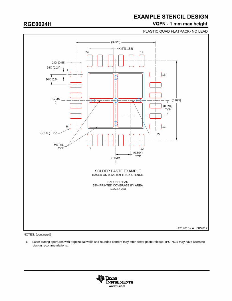
NOTES: (continued)
6. Laser cutting apertures with trapezoidal walls and rounded corners may offer better paste release. IPC-7525 may have alternate
design recommendations..
EXAMPLE STENCIL DESIGN
4219016 / A 08/2017
www.ti.com
VQFN - 1 mm max height
RGE0024H
PLASTIC QUAD FLATPACK- NO LEAD
SYMM
SYMM
SOLDER PASTE EXAMPLE
BASED ON 0.125 mm THICK STENCIL
EXPOSED PAD
78% PRINTED COVERAGE BY AREA
SCALE: 20X
(3.825)
(3.825)
(0.694)
TYP
(0.694)
TYP
4X ( 1.188)
1
6
712
13
18
1924
24X (0.24)
24X (0.58)
20X (0.5)
(R0.05) TYP
METAL
TYP
25
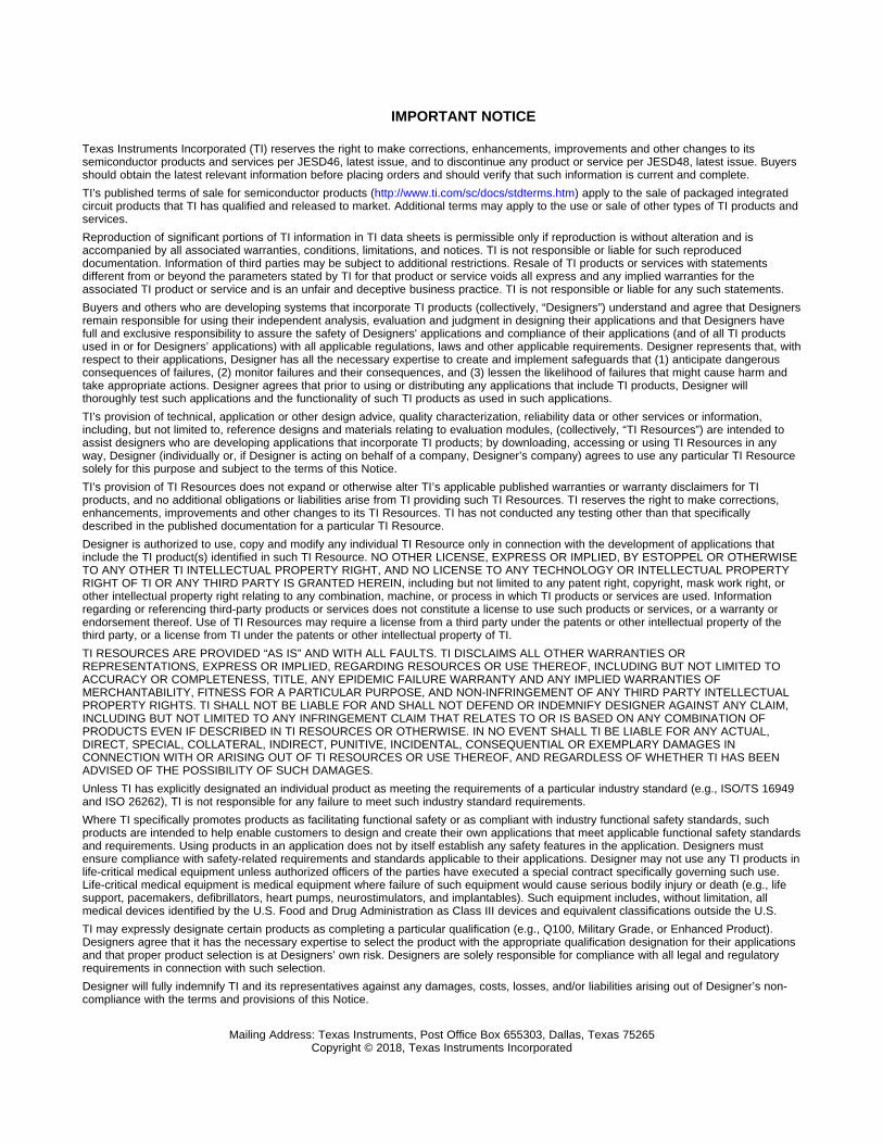
IMPORTANT NOTICE
Texas Instruments Incorporated (TI) reserves the right to make corrections, enhancements, improvements and other changes to itssemiconductor products and services per JESD46, latest issue, and to discontinue any product or service per JESD48, latest issue. Buyersshould obtain the latest relevant information before placing orders and should verify that such information is current and complete.TI’s published terms of sale for semiconductor products (http://www.ti.com/sc/docs/stdterms.htm) apply to the sale of packaged integratedcircuit products that TI has qualified and released to market. Additional terms may apply to the use or sale of other types of TI products andservices.Reproduction of significant portions of TI information in TI data sheets is permissible only if reproduction is without alteration and isaccompanied by all associated warranties, conditions, limitations, and notices. TI is not responsible or liable for such reproduceddocumentation. Information of third parties may be subject to additional restrictions. Resale of TI products or services with statementsdifferent from or beyond the parameters stated by TI for that product or service voids all express and any implied warranties for theassociated TI product or service and is an unfair and deceptive business practice. TI is not responsible or liable for any such statements.Buyers and others who are developing systems that incorporate TI products (collectively, “Designers”) understand and agree that Designersremain responsible for using their independent analysis, evaluation and judgment in designing their applications and that Designers havefull and exclusive responsibility to assure the safety of Designers' applications and compliance of their applications (and of all TI productsused in or for Designers’ applications) with all applicable regulations, laws and other applicable requirements. Designer represents that, withrespect to their applications, Designer has all the necessary expertise to create and implement safeguards that (1) anticipate dangerousconsequences of failures, (2) monitor failures and their consequences, and (3) lessen the likelihood of failures that might cause harm andtake appropriate actions. Designer agrees that prior to using or distributing any applications that include TI products, Designer willthoroughly test such applications and the functionality of such TI products as used in such applications.TI’s provision of technical, application or other design advice, quality characterization, reliability data or other services or information,including, but not limited to, reference designs and materials relating to evaluation modules, (collectively, “TI Resources”) are intended toassist designers who are developing applications that incorporate TI products; by downloading, accessing or using TI Resources in anyway, Designer (individually or, if Designer is acting on behalf of a company, Designer’s company) agrees to use any particular TI Resourcesolely for this purpose and subject to the terms of this Notice.TI’s provision of TI Resources does not expand or otherwise alter TI’s applicable published warranties or warranty disclaimers for TIproducts, and no additional obligations or liabilities arise from TI providing such TI Resources. TI reserves the right to make corrections,enhancements, improvements and other changes to its TI Resources. TI has not conducted any testing other than that specificallydescribed in the published documentation for a particular TI Resource.Designer is authorized to use, copy and modify any individual TI Resource only in connection with the development of applications thatinclude the TI product(s) identified in such TI Resource. NO OTHER LICENSE, EXPRESS OR IMPLIED, BY ESTOPPEL OR OTHERWISETO ANY OTHER TI INTELLECTUAL PROPERTY RIGHT, AND NO LICENSE TO ANY TECHNOLOGY OR INTELLECTUAL PROPERTYRIGHT OF TI OR ANY THIRD PARTY IS GRANTED HEREIN, including but not limited to any patent right, copyright, mask work right, orother intellectual property right relating to any combination, machine, or process in which TI products or services are used. Informationregarding or referencing third-party products or services does not constitute a license to use such products or services, or a warranty orendorsement thereof. Use of TI Resources may require a license from a third party under the patents or other intellectual property of thethird party, or a license from TI under the patents or other intellectual property of TI.TI RESOURCES ARE PROVIDED “AS IS” AND WITH ALL FAULTS. TI DISCLAIMS ALL OTHER WARRANTIES ORREPRESENTATIONS, EXPRESS OR IMPLIED, REGARDING RESOURCES OR USE THEREOF, INCLUDING BUT NOT LIMITED TOACCURACY OR COMPLETENESS, TITLE, ANY EPIDEMIC FAILURE WARRANTY AND ANY IMPLIED WARRANTIES OFMERCHANTABILITY, FITNESS FOR A PARTICULAR PURPOSE, AND NON-INFRINGEMENT OF ANY THIRD PARTY INTELLECTUALPROPERTY RIGHTS. TI SHALL NOT BE LIABLE FOR AND SHALL NOT DEFEND OR INDEMNIFY DESIGNER AGAINST ANY CLAIM,INCLUDING BUT NOT LIMITED TO ANY INFRINGEMENT CLAIM THAT RELATES TO OR IS BASED ON ANY COMBINATION OFPRODUCTS EVEN IF DESCRIBED IN TI RESOURCES OR OTHERWISE. IN NO EVENT SHALL TI BE LIABLE FOR ANY ACTUAL,DIRECT, SPECIAL, COLLATERAL, INDIRECT, PUNITIVE, INCIDENTAL, CONSEQUENTIAL OR EXEMPLARY DAMAGES INCONNECTION WITH OR ARISING OUT OF TI RESOURCES OR USE THEREOF, AND REGARDLESS OF WHETHER TI HAS BEENADVISED OF THE POSSIBILITY OF SUCH DAMAGES.Unless TI has explicitly designated an individual product as meeting the requirements of a particular industry standard (e.g., ISO/TS 16949and ISO 26262), TI is not responsible for any failure to meet such industry standard requirements.Where TI specifically promotes products as facilitating functional safety or as compliant with industry functional safety standards, suchproducts are intended to help enable customers to design and create their own applications that meet applicable functional safety standardsand requirements. Using products in an application does not by itself establish any safety features in the application. Designers mustensure compliance with safety-related requirements and standards applicable to their applications. Designer may not use any TI products inlife-critical medical equipment unless authorized officers of the parties have executed a special contract specifically governing such use.Life-critical medical equipment is medical equipment where failure of such equipment would cause serious bodily injury or death (e.g., lifesupport, pacemakers, defibrillators, heart pumps, neurostimulators, and implantables). Such equipment includes, without limitation, allmedical devices identified by the U.S. Food and Drug Administration as Class III devices and equivalent classifications outside the U.S.TI may expressly designate certain products as completing a particular qualification (e.g., Q100, Military Grade, or Enhanced Product).Designers agree that it has the necessary expertise to select the product with the appropriate qualification designation for their applicationsand that proper product selection is at Designers’ own risk. Designers are solely responsible for compliance with all legal and regulatoryrequirements in connection with such selection.Designer will fully indemnify TI and its representatives against any damages, costs, losses, and/or liabilities arising out of Designer’s non-compliance with the terms and provisions of this Notice.
Mailing Address: Texas Instruments, Post Office Box 655303, Dallas, Texas 75265Copyright © 2018, Texas Instruments Incorporated