Embed Size (px)
Citation preview
, r '- ' -'/- :
'K K~~--'~ - .--- ' .. 'N
i- - P-
K; \_Y /; f~ ?17/ 11~4--~ NAK«' 2/K ~ X-711-74-244/
-P Lkl p -.'.w'C B"\iAff U --D -x r- "' ,'j -N, - "r - " "' - .--
k/NN,' ~I 2, i & ;
l~ii .tI - \--
N'K ~" X"' - Ti~ ,. ~i ~~
,,SU 5,jf.- A.•E < t. .2-' FOR E
" ,- -N EELECT , , r > .
A -TM X -70 46)N7 -32677.
(NAS-T6 A HIGH VOLTAGEGPOWER
-- /- .'; -7 L:r-L -II-
SUPPLP FOR THE AE-C AND D.LO ENEEG'
Eo.- ;.E E LECT RON EXPERIENT. (NASA) 27 p HC
$45 CSCL 09E Unclas,- .G3/09 48008
/4-N -- :; --
.-- ,- -OEPH -__:;-_- , I E" t''4
ETONXP (NASA) ~27p7,-
)- , k ' ; _ .. ... .. .. - . .. ...7, Zx, (
" ... .. ?"~ -I- \ " .ju :- \ -/ ./
-p - HT N~~,-G AODARV E FLUa
(K'.G,/0 4800 2 -.
-E "LT :R r" ' , "_ ,
-I- .* ' :- - - .. ,. I'/ > , -/ ". r > 7*"'X-"- ' ,- >- ., -N- . .. __ .-.,
/1 -"-NV
-''_-" <''
,. , . -"' 7--.
,,~ ~ ~ ~ ~ ~ ~~~-- Y-,"-' ..., -,... x <:'
,'I / .-l .V . - ..-'.- - -" N B EL . ..... .'
~X'_-' /
" o :,U , I n-
A- -' .. a--.'K = . < ' "< -I > ,' , <
I~ ' ' N)I-.
2' / '., - 'K - / ,.'K.• " - ' , , .c.; / \ < - . .
NO -. .,' ... -. + ,. - , >% : -< - " , - '-.' :. - :7' - > , ,.-,.
'-7 -"-N _ - . . (7,. / -% . ---J IFLIGH CENTR 9
" < GRENEL 1 MAYLN
'7// N a-'- ~rs
https://ntrs.nasa.gov/search.jsp?R=19740024564 2018-06-13T22:21:42+00:00Z
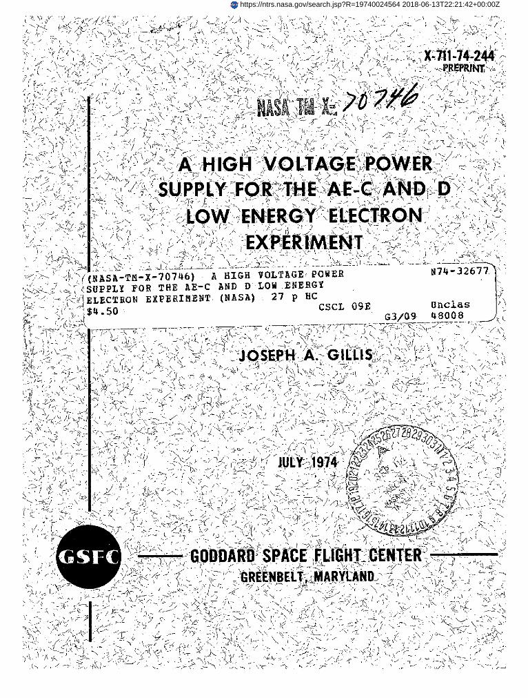
X-711-74-244
A HIGH VOLTAGE POWER SUPPLY FOR THE AE-C AND D
LOW ENERGY ELECTRON EXPERIMENT
Joseph A. Gillis
July 1974
GODDARD SPACE FLIGHT CENTERGreenbelt, Maryland
A HIGH VOLTAGE POWER SUPPLY FOR THE AE-CAND D LOW ENERGY ELECTRON EXPERIMENT
Joseph A. Gillis
FOREWORD
The purpose of this document is to describe the mechanicaland electrical design, and operation, of a high voltage powersupply for space flight use. The supply was used to generatethe spiraltron high voltage for the Low Energy Electron Ex-periment on AE-C and D. Two versions of the supply weredesigned and built, one referred to as the low power version(AE-C) and the other as the high power version (AE-D). Theformer was used on AE-C, while one of each version is usedon AE-D. Performance is discussed under all operatingconditions.
PRECEDING PAGE BLANK NOT FILMED
iii
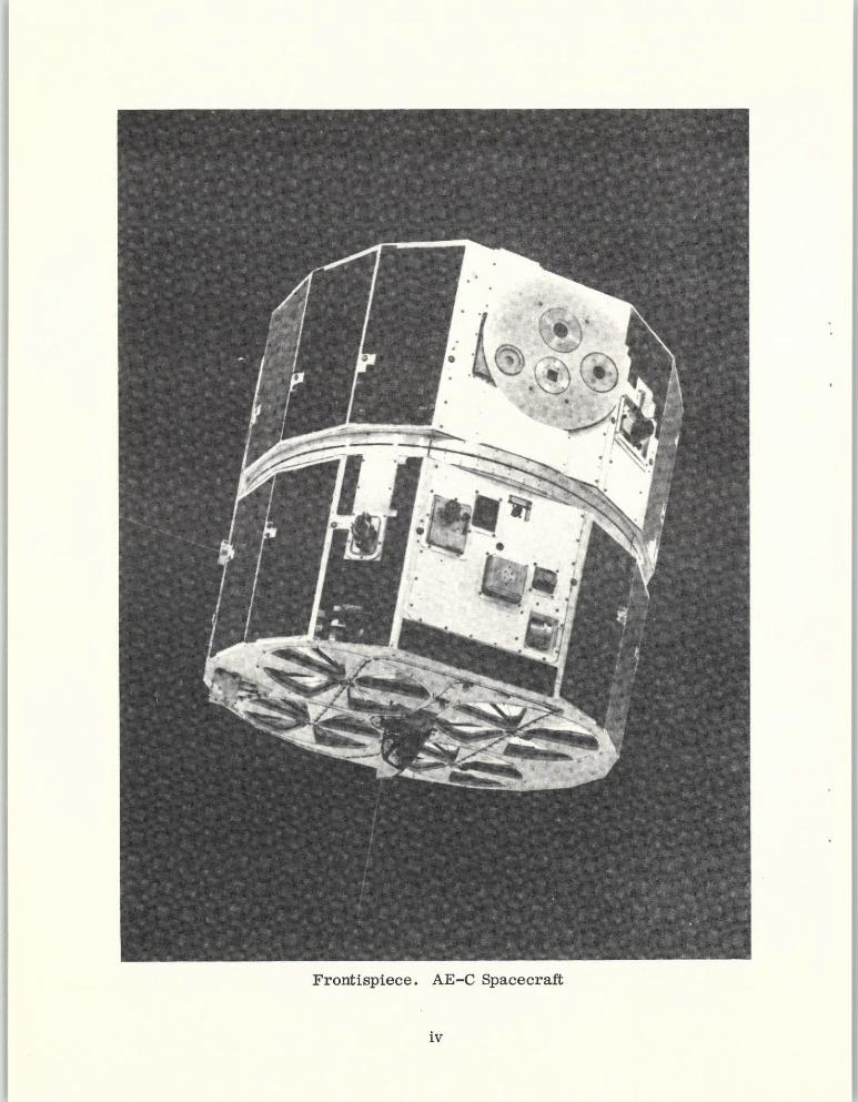
Frontispiece. AE-C Spacecraft
iv
CONTENTS
Page
FOREWORD ... ..... ... .. .... .. ...... ... iii
INTRODUCTION .......................... 1
ELECTRICAL DESIGN .................. .... 1
Design Specifications ... ... ............... 1
Circuit Description .. . . .. . . . . . . . . . .. . . .. . 2
MECHANICAL DESIGN AND LAYOUT . ............. . 6
PERFORMANCE DATA ...................... 14
APPENDIX A - HIGH VOLTAGE MATERIALS AND COMPONENTS . A-1
APPENDIX B - MAGNETIC COMPONENT DESIGN ......... . B-1
ILLUSTRATIONS
Figure Page
Frontispiece - AE-C Spacecraft . ................. iv
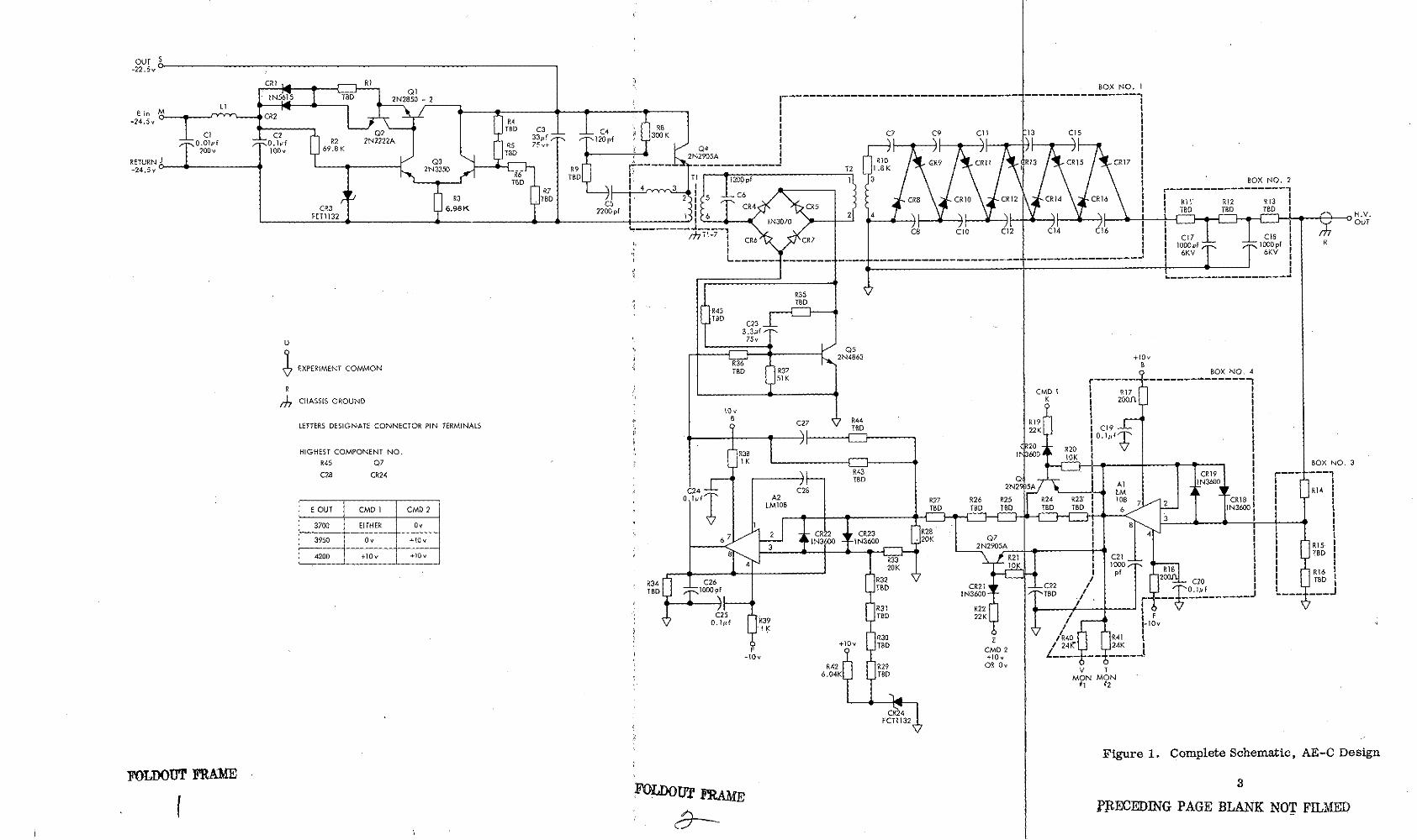
1 Complete Schematic, AE-C Design . ........... . 3
2 Modification to Schematic Used for the High Power(AE-D) unit . . . . . . . . . . . . . . . . . . . .. . . 6
3 General Mechanical Layout, Top View . ........ .. 8
4 Regulated Output Line Connection . ........... . 9
5(a-d) Finished Unit, AE-C SN02. . ............... . 10-13
6 Q4 Collector Current and Emitter to Collector Volts . .... 14
7 Q5 Emitter Current and Collector to Ground Voltage . .... 15
v
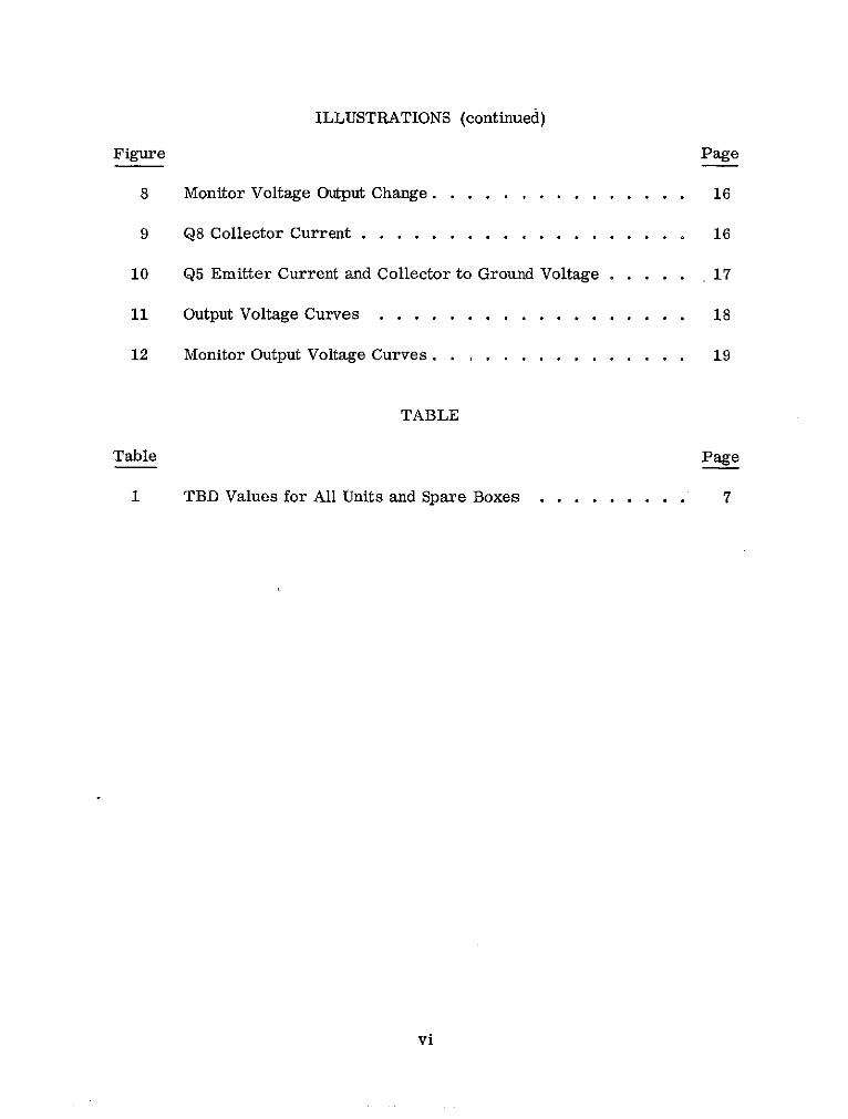
ILLUSTRATIONS (continued)
Figure Page
8 Monitor Voltage Output Change. . .......... ... . 16
9 Q8 Collector Current ................... 16
10 Q5 Emitter Current and Collector to Ground Voltage ..... 17
11 Output Voltage Curves .................. 18
12 Monitor Output Voltage Curves . . ............. 19
TABLE
Table Page
1 TBD Values for All Units and Spare Boxes .... . ... ... 7
vi
A HIGH VOLTAGE POWER SUPPLY FOR THE AE-C AND DLOW ENERGY ELECTRON EXPERIMENT
INTRODUCTION
High voltage power supplies have been a major part of spacecraft experimentelectrical systems since the first satellite left the launching pad, and a verylarge amount of experience has been gained. However, due to the very natureof high voltage in a space environment, this particular area remains today oneof the biggest and most persistent problem areas.
In a sense, each job is like delving into the field for the first time all overagain. No particular overall design approach at this time seems to have a de-cided advantage. Hardware must basically be tailored electrically and mechan-ically to conform to particular project- requirements. However, certain basicprincipals have emerged from experience as being sound engineering practice,and therefore desirable for incorporation in any design.
The electrical design used for the high voltage power supply discussed herein isfairly conventional and will be gone into only insofar as necessary to understandthe basic operation. The mechanical design is discussed in the hope that thetechniques used may be useful in the design of future high voltage power suppliesfor space use.
ELECTRICAL DESIGN
Design Specifications
Input Voltage: -24.5 volts -0.5 volts normally, with possible excursionsto -26.5 volts for indefinite periods and -50 volts for 10milliseconds.
Turn-on Transient: 0.5 amperes for not more than 15 milliseconds.
Input Current Limit: The input current will be positively limited to lessthan three times the quiescent value.
Reverse Polarity: The supply shall be protected against reverse polarityat the input.
Short Circuit Protection: No damage shall result from temporary or per-manent short circuit to common.
1
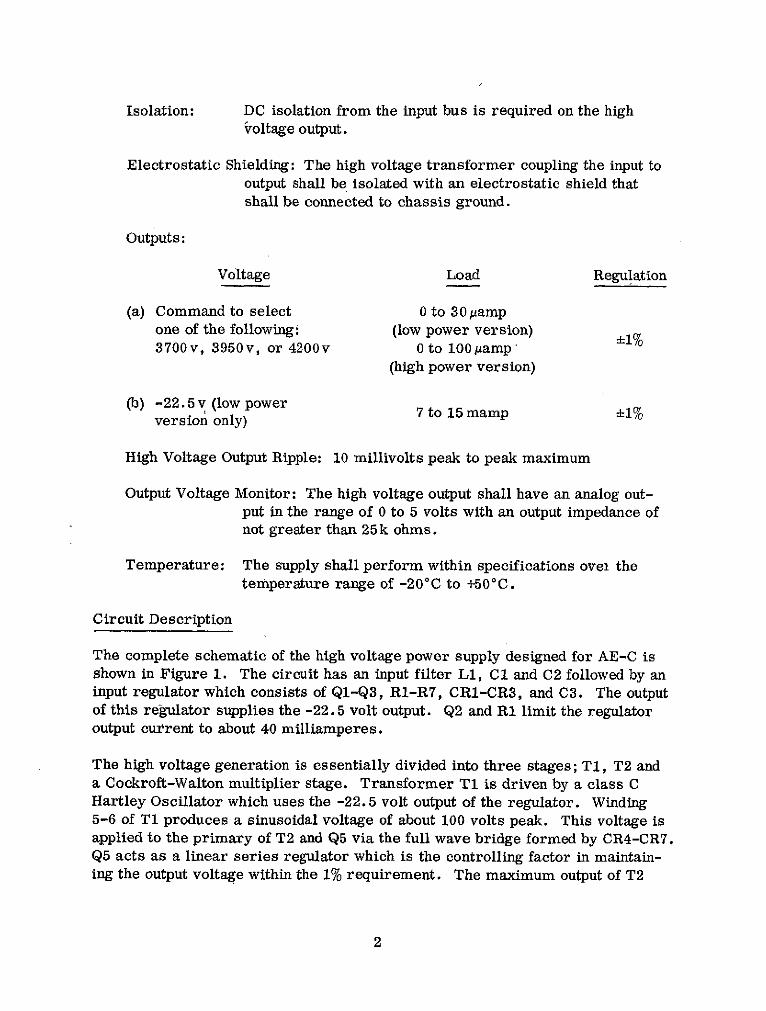
Isolation: DC isolation from the input bus is required on the highvoltage output.
Electrostatic Shielding: The high voltage transformer coupling the input tooutput shall be isolated with an electrostatic shield thatshall be connected to chassis ground.
Outputs:
Voltage Load Regulation
(a) Command to select 0 to 30 pampone of the following: (low power version)3700v, 3950v, or 4200v 0 to 100 pamp
(high power version)
(b) -22.5 v (low power 7 to 15 mampversion only)
High Voltage Output Ripple: 10 millivolts peak to peak maximum
Output Voltage Monitor: The high voltage output shall have an analog out-put in the range of 0 to 5 volts with an output impedance ofnot greater than 25k ohms.
Temperature: The supply shall perform within specifications ovei thetemperature range of -20oC to +50 0 C.
Circuit Description
The complete schematic of the high voltage power supply designed for AE-C isshown in Figure 1. The circuit has an input filter L1, C1 and C2 followed by aninput regulator which consists of Q1-Q3, R1-R7, CR1-CR3, and C3. The outputof this regulator supplies the -22.5 volt output. Q2 and R1 limit the regulatoroutput current to about 40 milliamperes.
The high voltage generation is essentially divided into three stages; T1, T2 anda Cockroft-Walton multiplier stage. Transformer T1 is driven by a class CHartley Oscillator which uses the -22.5 volt output of the regulator. Winding5-6 of T1 produces a sinusoidal voltage of about 100 volts peak. This voltage isapplied to the primary of T2 and Q5 via the full wave bridge formed by CR4-CR7.Q5 acts as a linear series regulator which is the controlling factor in maintain-ing the output voltage within the 1% requirement. The maximum output of T2
2
varies approximately from 440 volts to 480 volts peak depending on the outputload. This is multiplied by ten by the Cockroft-Walton multiplier to give a max-imum output of about 4600 volts with Q5 full on at room temperature and nominalload. R11, R12, C17 and C18 form a two stage output filter to maintain outputripple below the 10 millivolt peak to peak requirement. R11 and R12 were typ-ically around 330k ohms each. The filter therefore gives an effective attenua-tion of around 95db at the oscillator frequency of 20kHz. R13 is also around330 kohms and is used to limit current surges during arcing or accidental shorts.
The divider network for sensing the output voltage consists of R14 through R16.R14 is four metal oxide high voltage resistors in series of 470 megohms each.R15 plus R16 is about 2.2 megohms. This causes approximately 4 volts to ap-pear at the feedback point. Al acts as a unity gain buffer and presents a lowimpedance source for the monitor output and divider chain R23-R28. ZenerDiode CR24 forms the reference voltage which is divided down by R29-R33. Theoutput voltage level is controlled by appropriate c9mmands to Q6 and Q7. Theoutput of A2 drives Q5 in such a manner as to maintain the output within the re-quired tolerance.
Temperature compensation is accomplished by making R29 a diode, usually a1N4247. In some units this tends to overcompensate and a sensistor was usedin series for R30. R31 and R32 are adjusted to trim the output voltage. Theuse of a series regulator between two transformers has been used extensivelywith success by the Power Conversion and Control Section at the Goddard Flight-Space Center. It effectively gives isolation between input and output while con-trolling the voltage at a low level. It has the disadvantage, however, of havinga rather complex control loop which includes T2, the Cockroft-Walton multi-
plier, and the RC filters. This tends to give extensive phase shifting down tolow frequencies. The feedback loop must be compensated to substantially re-duce AC gain. To this end compensating network R35 and C23 are used betweenthe Q5 collector and base, and A2 uses a 0.47iuf capacitor for either C27 orC28. To further ensure stable closed loop operation, the DC gain of A2 is re-duced -somewhat from -its open loop value by use of R34, from pin 8 to ground,the value of which was typically one megohm.
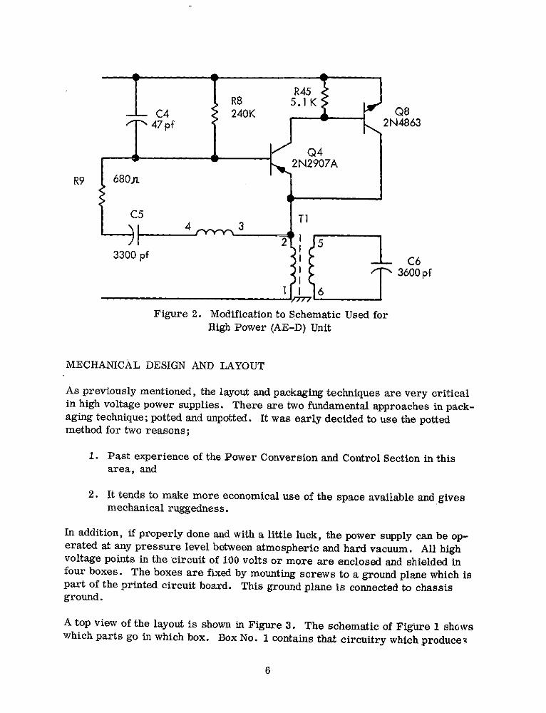
The circuit for AE-D is identical to that for AE-C except the Hartley oscillatoris beefed up by using a complementary connection as shown by Q4 and Q8 in
Figure 2. This was necessary in order to supply the increased output current(100 microamperes @ 4200 volts) called for in this unit. For the same reason,C6 is 3600pf to keep higher currents circulating in the tuned circuit. In addi-
tion, R1 is adjusted to limit the input regulator current to approximately 47milliamperes. All TBD values for each unit are shown in Table 1.
pRE ING pkGE BLANK NOT 5
R45R8 5.1 K
C4 240K Q847 pf 2N4863
Q42N2907A
R9 6801L
C5 T14 3
3300 pf '- C6I3600 pf
1 1 6Figure 2. Modification to Schematic Used for
High Power (AE-D) Unit
MECHANICAL DESIGN AND LAYOUT
As previously mentioned, the layout and packaging techniques are very criticalin high voltage power supplies. There are two fundamental approaches in pack-aging technique; potted and unpotted. It was early decided to use the pottedmethod for two reasons;
1. Past experience of the Power Conversion and Control Section in thisarea, and
2. It tends to make more economical use of the space available and givesmechanical ruggedness.
In addition, if properly done and with a little luck, the power supply can be op-erated at any pressure level between atmospheric and hard vacuum. All highvoltage points in the circuit of 100 volts or more are enclosed and shielded infour boxes. The boxes are fixed by mounting screws to a ground plane which ispart of the printed circuit board. This ground plane is connected to chassisground.
A top view of the layout is shown in Figure 3. The schematic of Figure 1 shcwswhich parts go in which box. Box No. 1 contains that circuitry which produces
6
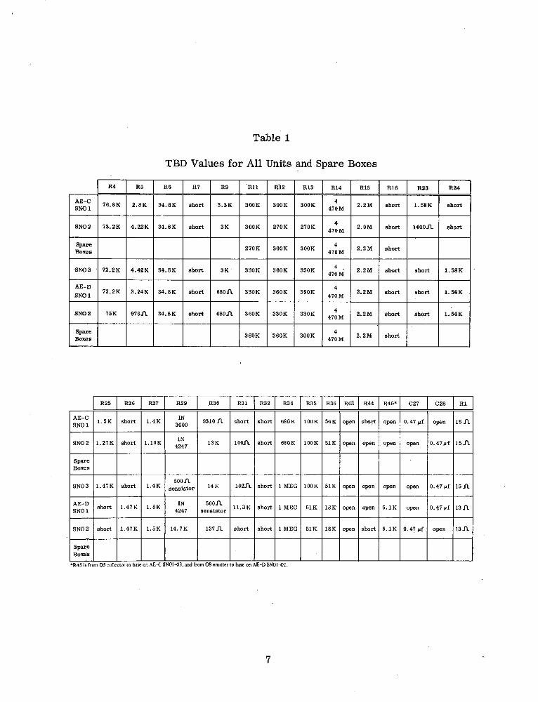
Table 1
TBD Values for All Units and Spare Boxes
R4 R5 R6 R7 R9 R11 R12 R13 R14 RI15 R16 R23 R24
AE-C 76.8K 2.8K 34.8K short 3.3K 300K 300K 300K 4 2.2M short 1.58K shortSNO 1 470M
SNO2 73.2K 4.22K 34.8K short 3K 300K 270K 270K 2.0M short 1400. short470M
Spare 4B 270K 300K 300K 47 2.2M shortBoxes 470M
SNO3 73.2K 4.42K 34.8K short 3K 330K 360K 330K 47M 2.2M short short 1.58K
AE-D 4SNOl 73.2K 3.24K 34.8K short 680.1n 330K 360K 390K 2.2M short short 1.58KSNO 1 470M
SNO2 75K 976. 34.8K short 680.1. 360K 330K 330K 2.2M short short 1.54K470M
Spare 360K 360K 300K 4 2.2M shortBoxes 470 M
R25 R26 R27 R29 R30 R31 R32 R34 R35 R36 R43 R44 R45* C27 C28 R1
AE-C 1.5K short 1.4K 3600 9310 1 short short 680K 100K 56K open short open 0.47pf open 15 .
INSNO2 1.27K short 1.13K 4247 13K 100.7. short 680K 100K 51K open open open open 0.47pf 15.f
SpareBoxes
500ASNO3 1.47K short 1.4K sensistor 14K 102.L short 1 MEG 100K 51K open open open open 0.47pf 15A
AE-D short 1.47K 1.5K 7 se500or 11.3K short 1 MEG 51K 18K open open 5.1K open 0.47mf 13ASNO 1 4247 sensistor
SNO2 short 1.47K 1.5K 14.7K 137A. short short 1 MEG 51K 18K open short 5.1K 0.47 pf open 13.n.
SpareBoxes
*R45 is from Q5 collector to base on AE-C SNOI-03, and from 08 emitter to base on AE-D SNOI-02.
7
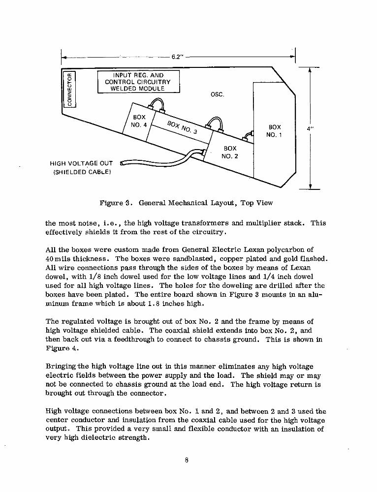
- 6.2"
ar INPUT REG. ANDCONTROL CIRCUITRY
WELDED MODULEz OSC.
BOXNO. 4 80) O3 BOX 4"
NO. 1
BOXNO. 2
HIGH VOLTAGE OUT
(SHIELDED CABLE)
Figure 3. General Mechanical Layout, Top View
the most noise, i.e., the high voltage transformers and multiplier stack. Thiseffectively shields it from the rest of the circuitry.
All the boxes were custom made from General Electric Lexan polycarbon of40 mils thickness. The boxes were sandblasted, copper plated and gold flashed.All wire connections pass through the sides of the boxes by means of Lexandowel, with 1/8 inch dowel used for the low voltage lines and 1/4 inch dowelused for all high voltage lines. The holes for the doweling are drilled after theboxes have been plated. The entire board shown in Figure 3 mounts in an alu-minum frame which is about 1.8 inches high.
The regulated voltage is brought out of box No. 2 and the frame by means ofhigh voltage shielded cable. The coaxial shield extends into box No. 2, andthen back out via a feedthrough to connect to chassis ground. This is shown inFigure 4.
Bringing the high voltage line out in this manner eliminates any high voltageelectric fields between the power supply and the load. The shield may or maynot be connected to chassis ground at the load end. The high voltage return isbrought out through the connector.
High voltage connections between box No. 1 and 2, and between 2 and 3 used thecenter conductor and insulation from the coaxial cable used for the high voltageoutput. This provided a very small and flexible conductor with an insulation ofvery high dielectric strength.
8
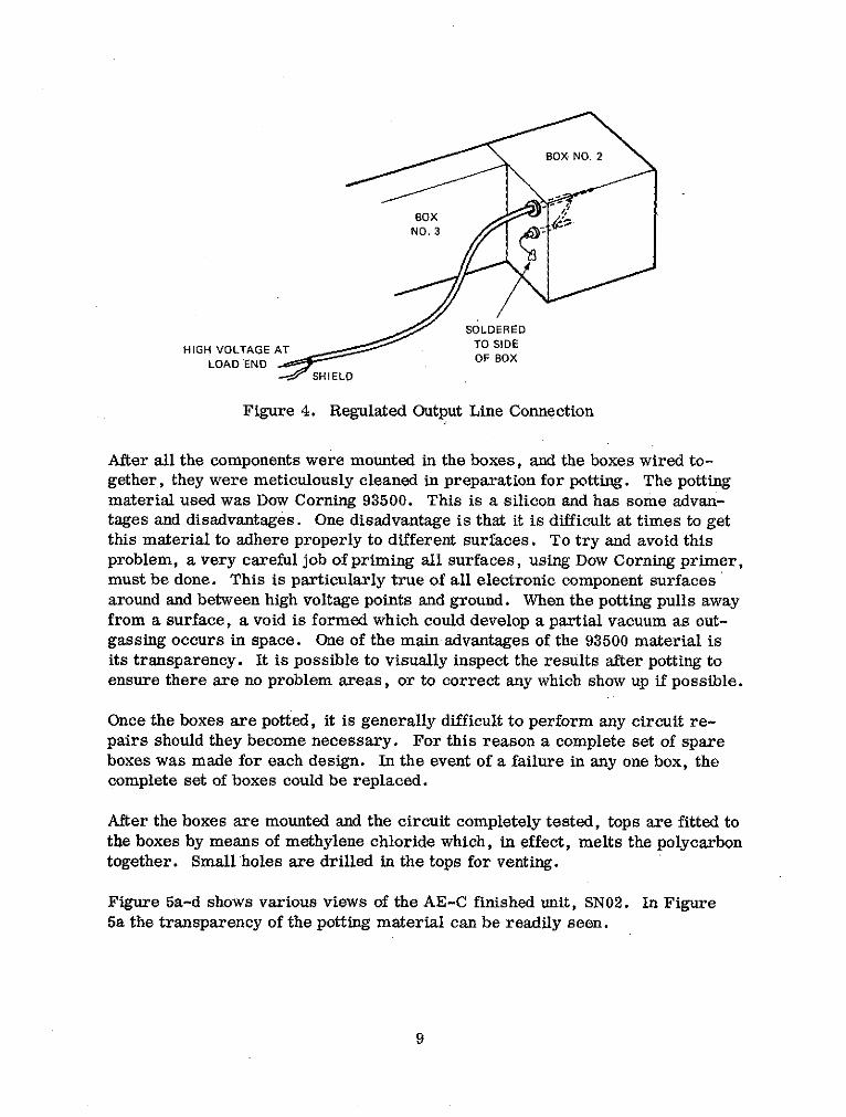
SOLDERED
HIGH VOLTAGE ATTO SIDE
LOAD END OF BOX
SHIELD
Figure 4. Regulated Output Line Connection
After all the components were mounted in the boxes, and the boxes wired to-gether, they were meticulously cleaned in preparation for potting. The pottingmaterial used was Dow Corning 93500. This is a silicon and has some advan-tages and disadvantages. One disadvantage is that it is difficult at times to getthis material to adhere properly to different surfaces. To try and avoid thisproblem, a very careful job of priming all surfaces, using Dow Corning primer,must be done. This is particularly true of all electronic component surfacesaround and between high voltage points and ground. When the potting pulls awayfrom a surface, a void is formed which could develop a partial vacuum as out-gassing occurs in space. One of the main advantages of the 93500 material isits transparency. It is possible to visually inspect the results after potting toensure there are no problem areas, or to correct any which show up if possible.
Once the boxes are potted, it is generally difficult to perform any circuit re-pairs should they become necessary. For this reason a complete set of spareboxes was made for each design. In the event of a failure in any one box, thecomplete set of boxes could be replaced.
After the boxes are mounted and the circuit completely tested, tops are fitted tothe boxes by means of methylene chloride which, in effect, melts the polycarbontogether. Small holes are drilled in the tops for venting.
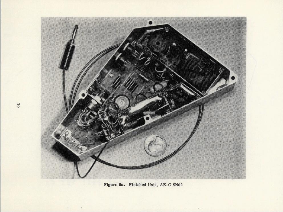
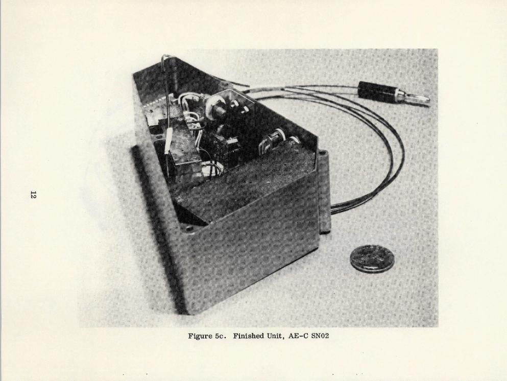
Figure 5a-d shows various views of the AE-C finished unit, SN02. In Figure5a the transparency of the potting material can be readily seen.
9
I-L
0I,-E
Fiue5.Fnsed Uni AEC N
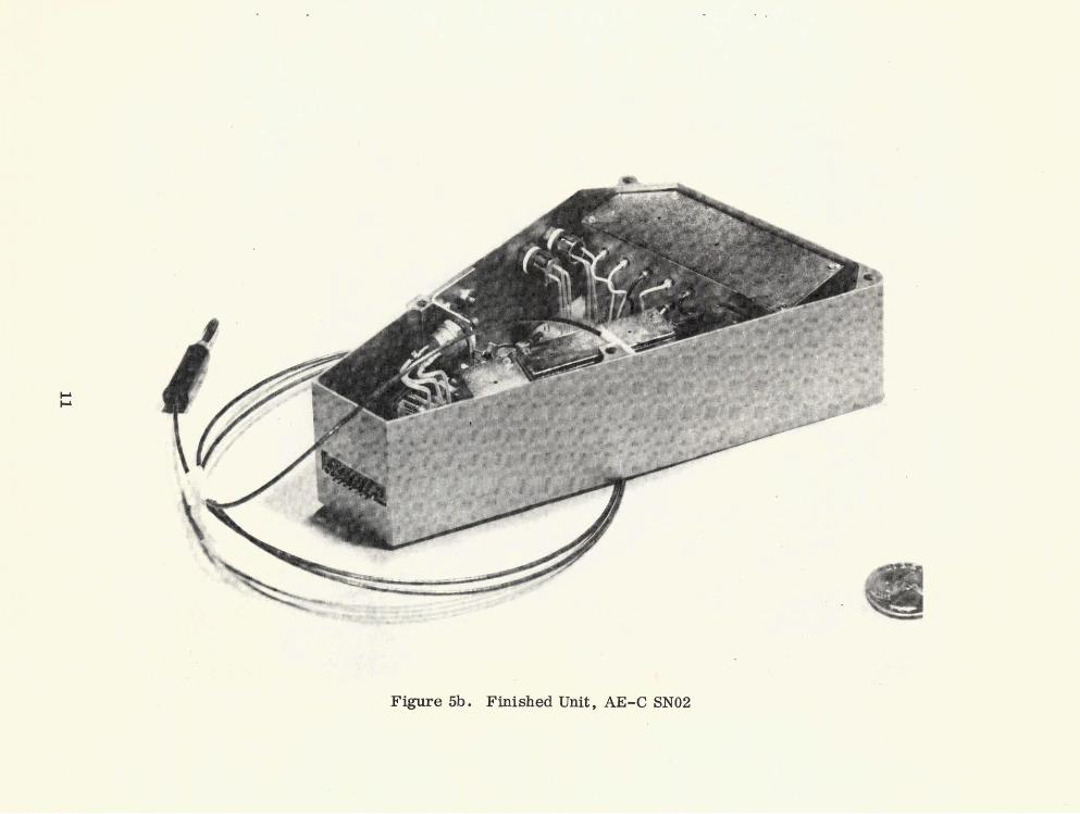
Figure 5b. Finished Unit, AE-C SNO2
~~i ~::-r~~~-__", -B - ~ ~~--Pa~~ ~~-a~~ .;8~D1
::::::::::: ::::::::i -::i:--:: ::~: ~~::~i:i
:: :::i-:;:::::::l~:'l:- isiii:ii:::: ::
::::: :
~I ~:Qs~~i
i;--i.---l- IC -Ller
: ~ztl~ ~: ~4-.~~e-~~~' ;'"li;- :9~_~="
:
FTp;ure 5c. Finished Unit, AE;-C SN02
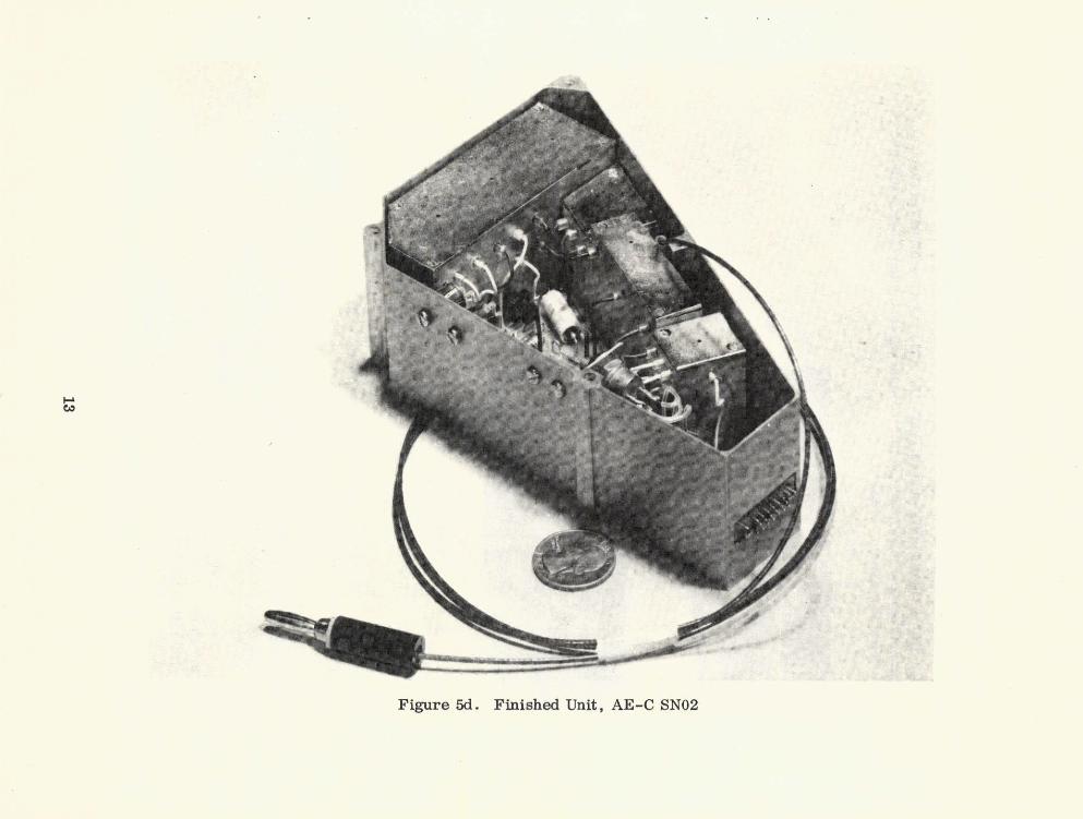
Figure 5d. Finished Unit AE-C SN
Figure 5d. Finished Unit, AE-C SN02
PERFORMANCE DATA
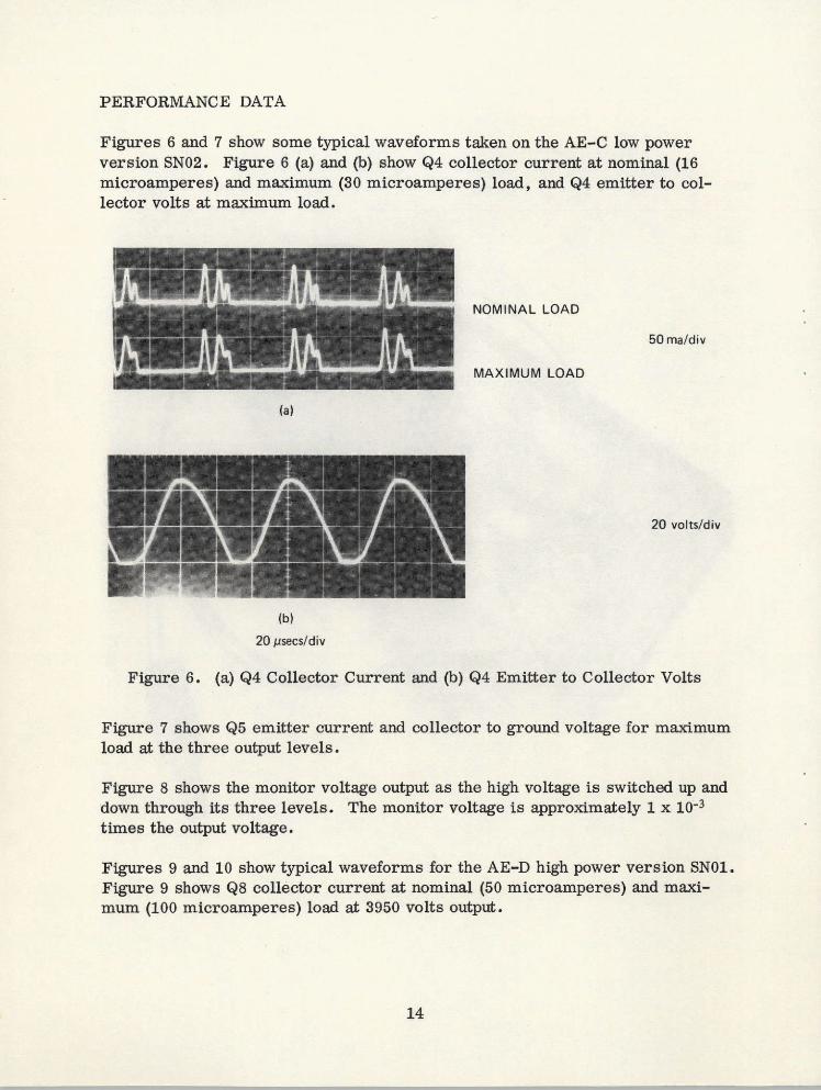
Figures 6 and 7 show some typical waveforms taken on the AE-C low powerversion SN02. Figure 6 (a) and (b) show Q4 collector current at nominal (16microamperes) and maximum (30 microamperes) load, and Q4 emitter to col-lector volts at maximum load.
NOMINAL LOAD
50ma/div
MAXIMUM LOAD
(a)
20 volts/div
(b)
20 psecs/div
Figure 6. (a) Q4 Collector Current and (b) Q4 Emitter to Collector Volts
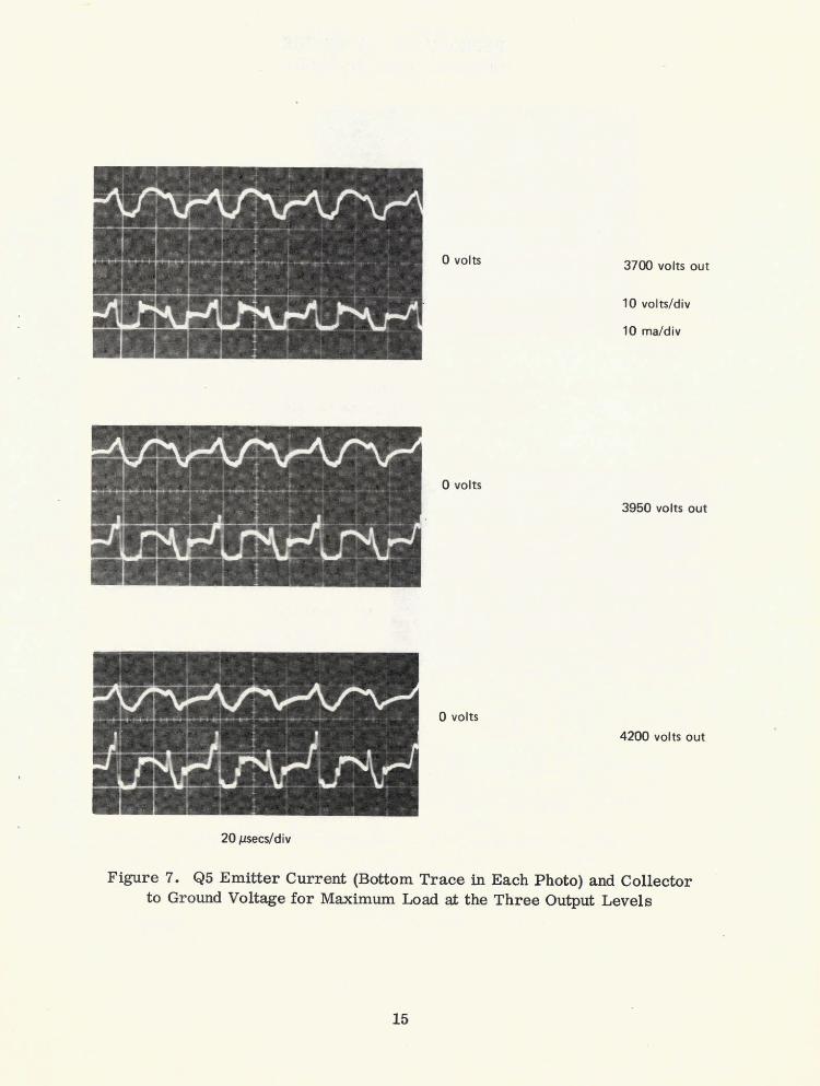
Figure 7 shows Q5 emitter current and collector to ground voltage for maximumload at the three output levels.
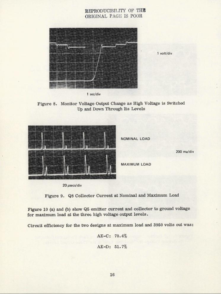
Figure 8 shows the monitor voltage output as the high voltage is switched up anddown through its three levels. The monitor voltage is approximately 1 x 10⁻³times the output voltage.
Figures 9 and 10 show typical waveforms for the AE-D high power version SNO1.Figure 9 shows Q8 collector current at nominal (50 microamperes) and maxi-mum (100 microamperes) load at 3950 volts output.
14
0 volts 3700 volts out
10 volts/div
10 ma/div
0 volts3950 volts out
0 volts
4200 volts out
20 psecs/div
Figure 7. Q5 Emitter Current (Bottom Trace in Each Photo) and Collectorto Ground Voltage for Maximum Load at the Three Output Levels
15
REPRODUCIBILITY OF THEORIGINAL PAGE IS POOR
1 volt/div
1 sec/div
Figure 8. Monitor Voltage Output Change as High Voltage is SwitchedUp and Down Through Its Levels
NOMINAL LOAD
200 ma/div
MAXIMUM LOAD
20 psecs/div
Figure 9. Q8 Collector Current at Nominal and Maximum Load
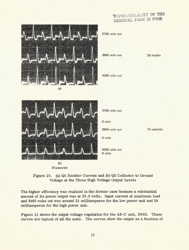
Figure 10 (a) and (b) show Q5 emitter current and collector to ground voltagefor maximum load at the three high voltage output levels.
Circuit efficiency for the two designs at maximum load and 3950 volts out was:
AE-C: 70.4%
AE-D: 51.7%
16
REPROUUCLILITY OF THIE
ORIGINAL PAGE IS POOR
3700 volts out
3950 volts out 20 ma/div
4200 volts out
(a)
3700 volts out
0 volts
3950 volts out 10 volts/div
0 volts
4200 volts out0 volts
(b)
20 lsecs/div
Figure 10. (a) Q5 Emitter Current and (b) Q5 Collector to GroundVoltage at the Three High Voltage Output Levels
The higher efficiency was realized in the former case because a substantialamount of its power output was at 22.5 volts. Input current at maximum loadand 3950 volts out was around 21 milliamperes for the low power unit and 28milliamperes for the high power unit.
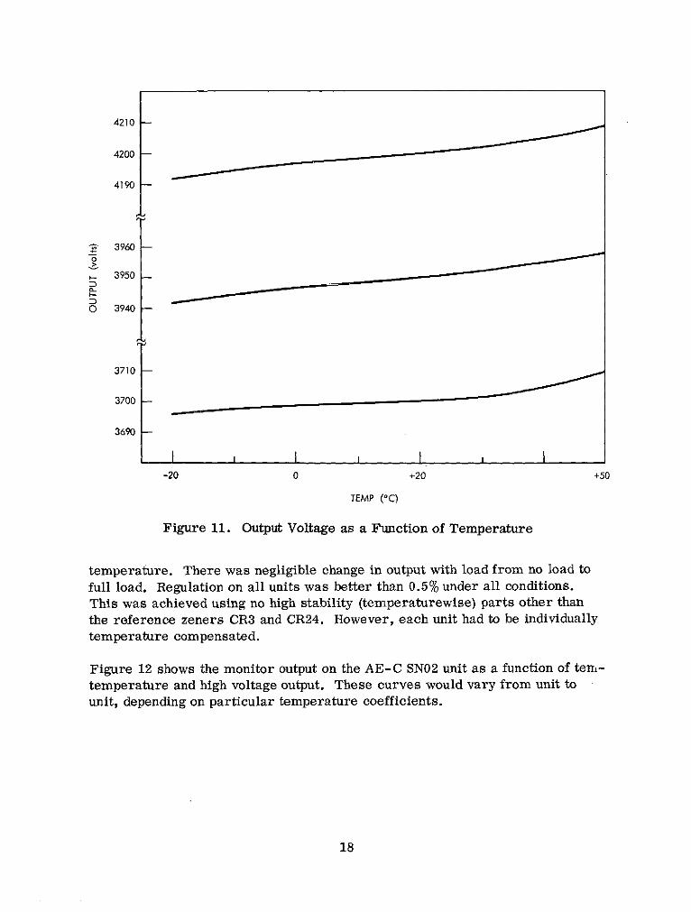
Figure 11 shows the output voltage regulation for the AE-C unit, SN02. Thesecurves are typical of all the units. The curves show the output as a function of
17
4210
4200
4190
3960
3950
0 3940
3710
3700
3690
I I I I
-20 0 +20 +50
TEMP (OC)
Figure 11. Output Voltage as a Function of Temperature
temperature. There was negligible change in output with load from no load tofull load. Regulation on all units was better than 0.5% under all conditions.This was achieved using no high stability (temperaturewise) parts other thanthe reference zeners CR3 and CR24. However, each unit had to be individuallytemperature compensated.
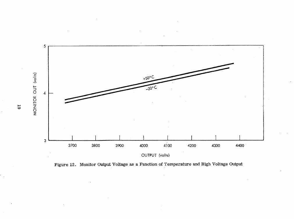
Figure 12 shows the monitor output on the AE-C SN02 unit as a function of tent-temperature and high voltage output. These curves would vary from unit tounit, depending on particular temperature coefficients.
18
550
.r-20° C0 40
0
3700 3800 3900 4000 4100 4200 4300 4400
OUTPUT (volts)
Figure 12. Monitor Output Voltage as a Function of Temperature and High Voltage Output
APPENDIX A
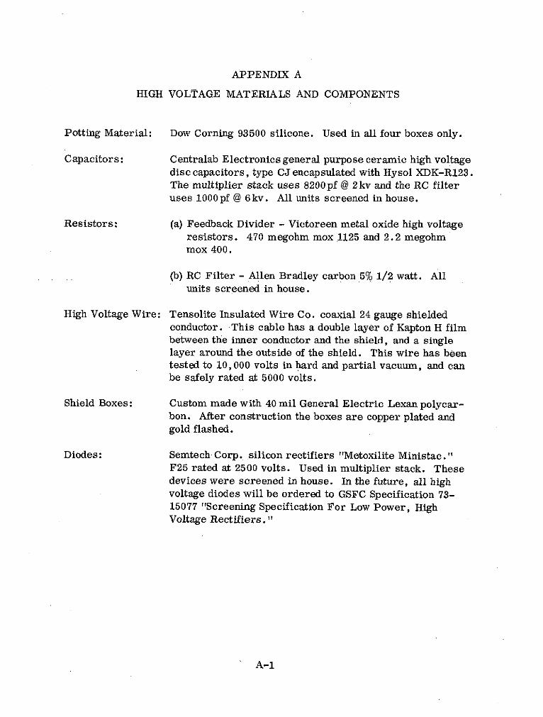
HIGH VOLTAGE MATERIALS AND COMPONENTS
Potting Material: Dow Corning 93500 silicone. Used in all four boxes only.
Capacitors: Centralab Electronics general purpose ceramic high voltagedisc capacitors, type CJ encapsulated with Hysol XDK-R123.The multiplier stack uses 8200pf @ 2kv and the RC filteruses 1000pf @ 6kv. All units screened in house.
Resistors: (a) Feedback Divider - Victoreen metal oxide high voltageresistors. 470 megohm mox 1125 and 2.2 megohmmox 400.
(b) RC Filter - Allen Bradley carbon 5% 1/2 watt. Allunits screened in house.
High Voltage Wire: Tensolite Insulated Wire Co. coaxial 24 gauge shieldedconductor. This cable has a double layer of Kapton H filmbetween the inner conductor and the shield, and a singlelayer around the outside of the shield. This wire has beentested to 10,000 volts in hard and partial vacuum, and canbe safely rated at 5000 volts.
Shield Boxes: Custom made with 40 mil General Electric Lexan polycar-bon. After construction the boxes are copper plated andgold flashed.
Diodes: Semtech Corp. silicon rectifiers "Metoxilite Ministac."F25 rated at 2500 volts. Used in multiplier stack. Thesedevices were screened in house. In the future, all highvoltage diodes will be ordered to GSFC Specification 73-15077 "Screening Specification For Low Power, HighVoltage Rectifiers."
A-1
APPENDIX B
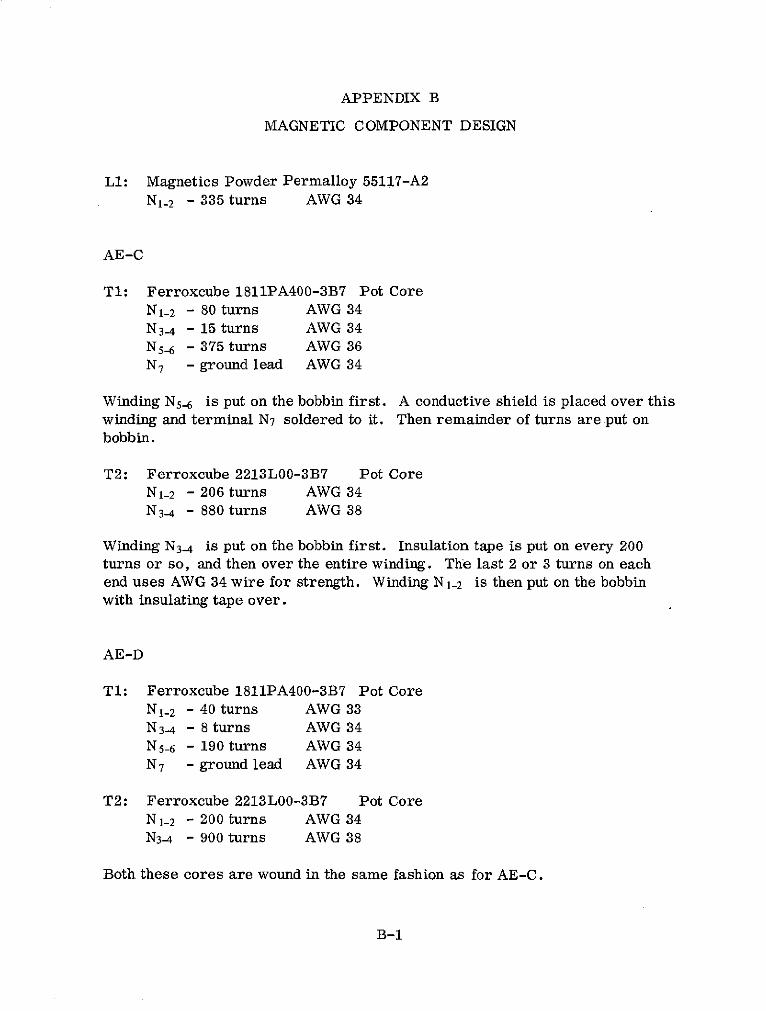
MAGNETIC COMPONENT DESIGN
L1: Magnetics Powder Permalloy 55117-A2N1- 2 - 335 turns AWG 34
AE-C
T1: Ferroxcube 1811PA400-3B7 Pot Core
N 1-2 - 80 turns AWG 34
N 3-4 - 15 turns AWG 34N 5 -6 - 375 turns AWG 36N 7 - ground lead AWG 34
Winding N 5-6 is put on the bobbin first. A conductive shield is placed over this
winding and terminal N7 soldered to it. Then remainder of turns are put onbobbin.
T2: Ferroxcube 2213L00-3B7 Pot CoreN1-2 - 206 turns AWG 34N 3-4 - 880 turns AWG 38
Winding N 3-4 is put on the bobbin first. Insulation tape is put on every 200turns or so, and then over the entire winding. The last 2 or 3 turns on eachend uses AWG 34 wire for strength. Winding N1- 2 is then put on the bobbinwith insulating tape over.
AE-D
T1: Ferroxcube 1811PA400-3B7 Pot Core
N1-2 - 40 turns AWG 33N 3-4 - 8 turns AWG 34N 5-6 - 190 turns AWG 34N 7 - ground lead AWG 34
T2: Ferroxcube 2213L00-3B7 Pot CoreN 1-2 - 200 turns AWG 34N3-4 - 900 turns AWG 38
Both these cores are wound in the same fashion as for AE-C.
B-1
OUT S-22.5v
BOX NO. 1
IN5615 -TBD 2N2850 -2 ------ -------LI 1-
Ein M CR2-
24.5 v R4
Cl C2 Q2 TBD C3 C4 300K C7 C9 C11 13 C15O.Olf O.Ipf R2 2N2222A R5 75X + 1 2
200v 100v 69.8 K TBD Q4S2N2905A
RETURN T Q - ---- RIO CR9 CR1i R13 CR15 CR17-24.5 v 2N3350 R9 T-2 1 .8K
TR T 1 200pf 1 3 BOX NO. 2
R7 I ------------R3 8D 2 5 6 CR8 CR10 CR12 CR14 CR16 I R11 R12 R13
CR3 6.98K 2200p I CR4 CR5 TBD TBD TDFEtT1132 2200p 1 6 2 4 I H.V.
I IN3070 I I I OUT
C6 C CS C10 C12 C14 C16 I ICR CR7 I C17 CS I 1000pf 1000pf R
I I I 6KV 6KVI-----------------------------------------------------------------.
R35TBD
4445TBD
3.39fU 75v
2N4863 +10vR36 B
EXPERIMENT COMMON T D R37O X N O 051K ------ -------------------
R CMD I R17
CHASSIS GROUND K 200 -f10v
LETTERS DESIGNATE CONNECTOR PIN TERMINALS C27 R44 R12T80 22K I19
R45 Q7 -_BOX NO. 3
C28 CR24 R43 9 C
EOUT CMD1 CMD 2 D TD TD TD TD N3600
3700 EITHER Ov 8
3950 Ov +10v 6 1
4200 +10v +10v RT8D4 R27 10K 1000
C25 TBD 22K / F
O.pf R39 / 10 v
R30 E /R40 R41S+10v TBD MD/ 24 4K
OUT OIT 366P-10v+L NK-- - OR42 R29 OR Ov IV T
#1 #2
CR24FCTl132
Figure 1. Complete Schematic, AE-C Design
FOLDOUT FRAME
3RECED0ING PAN3E BLANK NOT FLMED