Embed Size (px)
Citation preview
IBM Systems and Technology Group – EMC Center of Competency
© 2007 IBM Corporation
Importance of EMC Rule Checking in the PCB Design Process
Sam Connor
Senior Technical Staff Member
IBM Systems & Technology Group, Research Triangle Park, NC

IBM Systems and Technology Group – EMC Center of Competency
© 2007 IBM Corporation2
Outline
� EMC Rule Checking at IBM
– History
– Approach
– Importance
� PCB EMC Design Rule Checking Workflow
– Typical
– Optimized
� Process Improvement through Analytics

IBM Systems and Technology Group – EMC Center of Competency
© 2007 IBM Corporation3
History of EMC Rule Checking at IBM
� Knowledge of CAD data
� Expertise in computational geometry algorithms
Culture
� Emphasis on design specifications (workbooks)
� Emphasis on quality– How do you know design
guidelines were followed?
Research Staff
� Expertise in electromagnetics
� Numerical modeling of simplified structures
EDA Team
EMCEPca. 1992
Motivation
Rules
Implementation
IBM Systems and Technology Group – EMC Center of Competency
© 2007 IBM Corporation4
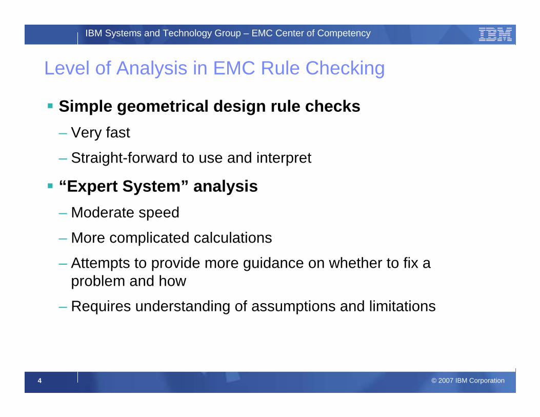
Level of Analysis in EMC Rule Checking
� Simple geometrical design rule checks
– Very fast
– Straight-forward to use and interpret
� “Expert System ” analysis
– Moderate speed
– More complicated calculations
– Attempts to provide more guidance on whether to fix a problem and how
– Requires understanding of assumptions and limitations
IBM Systems and Technology Group – EMC Center of Competency
© 2007 IBM Corporation5
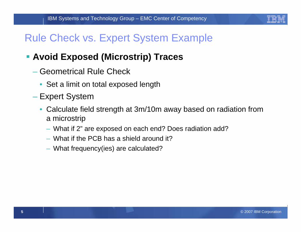
Rule Check vs. Expert System Example
� Avoid Exposed (Microstrip) Traces
– Geometrical Rule Check
• Set a limit on total exposed length
– Expert System
• Calculate field strength at 3m/10m away based on radiation from a microstrip– What if 2” are exposed on each end? Does radiation add?
– What if the PCB has a shield around it?
– What frequency(ies) are calculated?

IBM Systems and Technology Group – EMC Center of Competency
© 2007 IBM Corporation6
Goal of EMC Rule Checking� Identify violations of design rules and sort them
– Fix most severe violations
– Minimize risk of failure without overdesigning product
� Tell me if my product is going to pass EMI testing
� Challenges:
– Cannot simulate entire system with all relevant details
– Extrapolating from local effects on PCB to far-field performance
– Products have unique characteristics
• Airflow requirements
• Cables/connectors
• Materials

IBM Systems and Technology Group – EMC Center of Competency
© 2007 IBM Corporation7
Importance of EMC Rule Checking
� PC group was NOT using EMCEP– Developed on x86 hardware & Windows OS
but EMCEP was UNIX-only– Shorter development cycle than
server/mainframe systems
– RESULT:• 5-7 PCB revisions over development cycle• Consistently failed 1st set of EMC testing• 1-2 PCB revisions specifically for EMC fixes
� After adopting EMCEP/EMSAT…– 1-2 fewer PCB revisions– Consistently passed 1st set of EMC testing
© Jonathan Zander / Wikimedia Commons / CC-BY-SA-2.5 / GFDL
IBM Systems and Technology Group – EMC Center of Competency
© 2007 IBM Corporation8
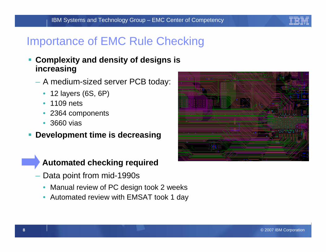
Importance of EMC Rule Checking
� Complexity and density of designs is increasing
– A medium-sized server PCB today:• 12 layers (6S, 6P)• 1109 nets• 2364 components• 3660 vias
� Development time is decreasing
� Automated checking required
– Data point from mid-1990s• Manual review of PC design took 2 weeks• Automated review with EMSAT took 1 day

IBM Systems and Technology Group – EMC Center of Competency
© 2007 IBM Corporation9
Typical PCB Design Process
Prototype Design Validation System Integration
Benchtop
Limited functionality
Measure preliminary spectrum
Soft-tooled system
Basic functionality
Run full battery of EMC tests
Production-level system
Full functionality
Run EMC certification tests
Run EMC Design Rule Check
- Length of time varies (longer is better)

IBM Systems and Technology Group – EMC Center of Competency
© 2007 IBM Corporation10
EMC Design Rule Checking Tasks/Workflow� Rule configuration (1-2 minutes)
– Setup limits and options to suit the product technology– Not a per-product effort
• Asynchronously adjusted as an ongoing research effort
� Design classification or “tagging” (2-4 hours)– Schematics, net lists, experience– Boolean expressions and wildcard string matching to
find nets & components
� Run rules (1-60 minutes)– Repeat for all rule configurations necessary
� Review violations (2-4 hours)– View violations with context (in design view)– Look for patterns (repeated design features)– Prioritize violations
• Number of fixes is often limited

IBM Systems and Technology Group – EMC Center of Competency
© 2007 IBM Corporation11
Quantify Violation Severity
� Sometimes deeper analysis of violation is required
– Analytical formula
– Full-wave modeling
� Preferences
– Fast analysis
– Model generated from violation geometry data
– Easy to create hypothetical solutions and compare

IBM Systems and Technology Group – EMC Center of Competency
© 2007 IBM Corporation12
Optimized EMC Design Rule Checking Workflow
� Reduce time required to classify design
– Enforce naming conventions on design teams
• Tagging can be done automatically with scripts (1-2 minutes)
� Reduce time required to review violations
– Apply post-processing algorithms to violation list
• Eliminate commonly ignored violations based on recognizable messages or patterns

IBM Systems and Technology Group – EMC Center of Competency
© 2007 IBM Corporation13
Process Improvement through Analytics
� Continual process improvement
– Needs feedback loop
� Benefits:
– Measurable improvements to tool
– More effective usage of tool
CollectPerformance
Data
Adjust Rulesand/or
Settings
Run RuleCheckson PCB
MonitorAverage
Performancevs Target

IBM Systems and Technology Group – EMC Center of Competency
© 2007 IBM Corporation14
Monitor Average Performance
� Good profile ( green circle)– Green and red bars close to the same, with blue bar
somewhat higher (conservative checking)
� Bad profiles ( red circle and red arrows)– Green and red bars close to zero, with blue bar much higher
0
10
20
30
40
50
60
70
80
90
100
Ave
rage
Num
ber
# of Vios Found by EMSAT
# of Vios with Fix Requested
# Vios Fixed by Development
404107� Blue bars : number of
violations found by the rule-checking S/W
� Green bars : number of violations that were considered important (fix requested)
� Red bars : number of violations actually fixed
IBM Systems and Technology Group – EMC Center of Competency
© 2007 IBM Corporation15
Summary
� EMC design rule checking is an essential part of IBM’s PCB design process
� Rule checking should be run as early as possible
� Most time is spent “tagging” a design and reviewing results– Using naming conventions for nets and components can
dramatically improve efficiency of tagging process
– Post-processing results data to reduce violation list improves efficiency of violation review process
� Analyzing results trends helps improve quality and efficiency of rule checking

IBM Systems and Technology Group – EMC Center of Competency
© 2007 IBM Corporation16
Backup Slides

IBM Systems and Technology Group – EMC Center of Competency
© 2007 IBM Corporation17
Signal Reference Rules
� Critical nets must not cross a split in the adjacent reference plane
� Critical nets must not change reference planes
� Critical nets must not be within a specified distance of the edge of their reference plane

IBM Systems and Technology Group – EMC Center of Competency
© 2007 IBM Corporation18
Wiring and Crosstalk Rules
� Critical nets must not be routed within a specified distance from an I/O net
� Critical nets must be buried between solid planes
� Critical nets must be isolated from other nets by a specified distance

IBM Systems and Technology Group – EMC Center of Competency
© 2007 IBM Corporation19
Differential Wiring and Mode Conversion Rules
� Differential vias must have symmetrically placed return vias
� Differential critical nets must be routed within a specified distance of each other, and the length of the mates must match within a specified amount (running skew)
+
-

IBM Systems and Technology Group – EMC Center of Competency
© 2007 IBM Corporation20
Decoupling Rules
� Decoupling capacitors must be placed between all adjacent plane pairs within a specified grid densit y (spatial decoupling)
� A decoupling capacitor must be placed within a specified distance from each IC power pin
� The trace connecting between a capacitor (or IC) pi n and its via to the power/ground-reference plane mus t be no longer than the specified distance

IBM Systems and Technology Group – EMC Center of Competency
© 2007 IBM Corporation21
Placement Rules
� Filters must be placed close to the I/O connector pins they are filtering
� Certain devices must be placed a specified distance away from other devices or from I/O connectors
– Analog and digital isolation
– Prevent coupling of ASIC emissions to I/O signals
I/O
F
I/O
ASIC