Embed Size (px)
Citation preview
Systems
GA22-7010-4 File No. S/370-01
IBM System/370 Model 168 Functional Characteristics

Page of GA22-70104 Revised June 18, 1976 By TNL: GN22-0514
Preface
This manual describes the functional characteristics and features of the IBM System/370 Model 168. The purpose of this manual is to provide management, programmers, and operations personnel with a fundamental understanding of this System/370 model.
Details concerning the use of programming and peripheral equipment are not given in this manual; however, a partial list of relevant manuals is given in "Appendix A, Bibliography," and programming is outlined in "Programming."
This manual is divided into these sections: • "Introduction," giving an overall picture of the system.
• "Basic System Description," giving configuration, facilities, features, and system highlights of the Model 168.
• "Central Processing Unit," describing the processing unit (the processor storage control function, processor storage, instruction unit, and execution unit), and including virtual storage and dynamic address translation.
Fifth Edition (January 1976)
• "Channel Description," describing the selector, byte multiplexer, and block multiplexer channels, and data rate considerations.
• "Functions," describing usage metering, modeldependent functions, the system console, and the operator's console.
• The Appendixes, which provide useful supplementary tables as well as information about the multiprocessing feature, the integrated storage control feature, the power warning feature, the attached processor feature, and the deviations from the Model 168 functional characteristics.
The reader is assumed to have an understanding of data processing systems including fundamental knowledge of IBM System/370 as defined in IBM System/370 Principles of Operation, GA22-7000.
This is a major revision of GA22-7010-3 and all previous editions, including Technical Newsletters GN22-0477, GN22-0485, and GN22-0491, making them obsolete. A new section, AppendixG, describes the IBM 3062 Attached Processing Unit (APU) Modell. Changes have been made throughout this manual to describe the integration of that unit into the system to create the Model 168 Attached Processor System. A technical change to the text or to an illustration is indicated by a vertical line to the left of the change.
Changes are periodically made to the information herein; before using this publication in connection with the operation of the System/370, consult the IBM System/370 Bibliography, GC20-0001, for editions that are applicable and current.
Requests for copies of IBM publications should be made to your IBM representative or to the IBM branch office serving your locality.
This manual has been prepared by the IBM System Products Division, Product Publications, Dept. B98, PO Box 390, Poughkeepsie, N.Y. 12602. A form for readers' comments is provided at the back of this publication. If the form has been removed, comments may be sent to the above address. Comments become the property of IBM.
©Copyright International Business Machines Corporation 1972, 1973, 1976
Introduction Attachable Input/Output Devices
Programming Programming Compatibility between This System, Other System/370 Models, and System/360
Basic System Description System Configuration Optional Features Standard Facilities .
System Timing Facilities System Highlights
General Data Data Storage
Central Processing Unit Processor Storage
Models Permanent Storage Assignment Interleaving . Configuration Capability
Processor Storage Control Function Buffer Storage Control High-speed Buffer Translator Translation Lookaside Buffer (TLB) TLB Operation . I/O Channel Controls (I/O Buffer) Processor Storage Controls
Instruction Unit (I-unit) Execution Unit (E-unit)
Local Storage Writable Control Storage
Extended Control Dynamic Address Translation
Service Processor (SVP)
Channel Description Channels.
Channel Attachment Indirect Data Addressing 2860 Selector Channel . 2870 Byte Multiplexer Channel 2880 Block Multiplexer Channel
Functions . Usage Metering Model-dependent Functions
Logout Machine Check (Switch) Hardware Retry Software Retry .
Details of Machine Checks Machine-check Condition Masking Machine-check Control Register Bits . Allocation of Control Register Fields
System Console with CRT Display Operator's Console Operations Indicators Status Byte Sense Byte
5 5 5
5
6 6 6 8 9
10 10 10
11 11 11 12 12 12 13 13 13 14 14 14 15 16 16 16 16 16 16 16 16
. 17 17, .
17 18 18 19 20
21 21 22 22 22 22 22 24 24 24 24 26 27 27 28 29 29
Page of GA22-7010-4 Revised June 18, 1976 By TNL: GN22-0514
Contents
Synchronous Checks 29 Asynchronous Checks 29 Interruptions 29
Appendix A. Bibliography 31 General 31 IBM Operating System (OS/VS) 31 Representative I/O Devices 31
Appendix B. Controls and Indicators 32
Appendix C. Glossary and Abbreviations 39
Appendix D. Integrated Storage Control Feature 41 Facilities . 41 Statistical Usage/Error Recording 42 Storage Control Diagnostic Tests . 43 Configuration Control . 43 Interface Time-out Considerations 43 Input/Output Operations 43
Appendix E. Multiprocessing Feature 45 Usage Meter . 45 Multisystem Activity Monitor (MSAM) 45 Prefixing. 45 CPU Signaling and Response 46 Shared Storage 46 Storage Control . 46 Storage Protect . 46 Malfunction Alert 46 Time-of-day Clock 46 Power Control 46 MCU Power Control 47 Resets 47 Channel Control Reconfiguration 48
Configuration Control 48 System Mode 48
Appendix F. Power Warning Feature 51
Appendix G. Attached Processor Feature 52 Usage Meter . 52 System Activity Meter (SAM) . 52 Prefixing. 52 CPU Signaling and Response 52 Processor Addresses 53 Storage Control . 53 Malfunction Alert 53 Time-of-day (TOD) Clock 53 Power Control 53
Appendix H. Deviations from the IBM System/370 Model 168 Functional Characteristics 54
Store CPU ID (STIDP) Instruction 54 Interruptions When the Processor Leaves the
Stopped State . 54 Data Exception during Execution of a Divide Decimal
Instruction 54 Check-stop Control . 54 Serialization for a Write Direct Instruction 54 Enable System Clear Pushbutton 54
Index 55

Representative Installation Using the IBM System/370 Model 168 Uniprocessinl System with Typical 110 Units
Representative Installation Using the IBM SYltem/370 Model 168 Attached Processor System with Typical I/O Units

The IBM System/370 Model 168 (Frontispiece) is an upward-compatible information processing system, designed for high-speed, large-scale scientific and business applications. The improved speed and power result primarily from the monolithic processor storage, high-speed logic circuitry, dynamic address translation (providing an address space of up to 16,777,216 bytes), concurrency of operations, and use of efficient algorithms. This model can serve as a compatible growth system for installed System/ 360 and System/370 models.
Contributing significantly to the increased efficiency are the processor (real) storage capacities, which range from 1,048,576 bytes (l,024K) to 8,388,608 bytes (8,192K), and a high-speed buffer that holds currently used sections of processor storage, making data available in less time. Speed is further increased by the use of interleaved processor storage elements.
For input/output operations, the system (with the extended channels feature) may connect a maximum of 12 channels: one or two byte multiplexer channels, as many as six selector channels, or up to 11 block multiplexer channels. These channels use dedicated channel data buffers in the CPU to achieve increased aggregate data rates through the effective use of the four-way interleaved processor storage. A further increase in aggregate data rates and external cabling flexibility is achieved with the channel dual-bus facility.
The performance of a Model 168 may be further enhanced by the addition of an instruction processor, the IBM 3062 Attached Processing Unit Modell. The attached processing unit shares the storage of its host CPU, and programs may be executed simultaneously on both units.
Multiprocessing (MP) is available as an option. With MP installed on two Model 168 systems, programs may be executed simultaneously in each CPU and may share system resources (CPUs, I/O devices, storage, and data). System availability is improved through versatile utilization of th,ese resources. Secondary benefits derived from MP include operational efficiency and flexibility.
Attachable I nput/Output Devices
The I/O devices that can be attached to Model 168 are listed in the IBM System/370 Input/Output Configurator, GA22-7002.
PROGRAMMING
Programming support for this model includes Operating System/Virtual Storage (OS/VS). This system uses dynamic address translation and the new control f~nctions to provide the virtual storage capability.
In addition to OS/VS, Operating System (OS) provides basic System/370 support (basic control mode) without
Page of GA22-7010-4 Revised June 18, 1976 By TNL: GN22-0S14
Introduction
invoking the extended control functions. In order to provide recovery support, these control programs must be at the proper level.
Programming support for the APU is provided by an update to the latest level of OS/VS2 Release 3.
Programming support for multiprocessing is provided by OS/VS2 Release 2.
Programming Compatibility between This System, Other System/370 Models, and System/3GO
Given the storage capacity, the internal and input/output channel processing rates, and the types of attachable input/output devices, compatibility can be maintained with other System/370 and System/360 models. These are the exceptions: 1. Programs using machine-dependent data (for example,
machine logouts). 2. Programs using the ASCII bit (PSW bit 12). 3. Programs that depend upon features or I/O devices that
are not implemented on this system (such as special instructions for the System/360 Model 44).
4. Programs that depend upon validity of data after the system power has been turned off and restored.
Programs written for other System/370 or System/360 models that contain the following conditions or requirements should be evaluated on an individual basis to ensure proper operation: 1. Time-dependent programs. 2. Programs written to cause deliberate program checks. 3. Programs that depend upon model-dependent features
of other System/370 and System/360 models. 4. Programs that use storage locations between addresses
128 (decimal) and 1927 (decimal) after a diagnostic logout into program storage. However, these programs may be executed: a. If MACHINE CHECK is set to STOP ON CHK. In
this case, no diagnostic logout into program storage takes place.
b. If program-storage locations that are overlaid by the diagnostic logout are restored with the program requirements before an IPL and program restart.
Any attempt to continue processing after a diagnostic logout to program storage without restoring your program information to the logout area will have unpredictable results. 5. Programs whose CCW chains are dynamically modified
may not run in the virtual address space. To run such programs under OS/VS, the "virtual = real" option may have to be used.
The 1,416 bytes (between locations 512 and 1927) of the machine-check extended logout (MCEL) area can be moved into another program-storage area. The technique used to accomplish this relocation depends upon your application.
Introduction 5
Basic System Description
SYSTEM CONFIGURATION (FIGURE 1)
The IBM System/370 Model 168 Data Processing System includes: • 3066 System Console Model 2 or 3
An L-shaped grouping which includes the operator's console, main control panel, document and indicator console, main control panel, document and indicator viewers, storage configuration control panel, and console file (see "Functions").
• 3168 Processing Unit Modell or 3 This CPU contains the processor storage control function (PSCF), processor storage, instruction unit, and execution unit (see "Central Processing Unit").
• 3067 Power and Coolant Distribution Unit Model 2, 3, or S.
• Channels (see "Channel Description").
• Relevant I/O Units (see IBM System/370 Input/Output Configurator, GA22-7002).
• Optional Operating System (see "Programming").
OPTIONAL FEATURES
IBM System/370 Model 168 optional features include:
709/1090/1094/1094 II Compatibility
This optional feature, in conjunction with its integrated emulator program, allows the Model 168 CPU to execute programs and programming systems originally written for other systems. See IBM System/370 Special Feature Description-709/7090/7094/7094 II Compatibility Feature for IBM System/370 Models 165, 165 II, and 168. GA22-69SS.
7070/7074 Compatibility
This optional feature, in conjunction with its integrated emulator program, allows the Model 168 CPU to execute programs and programming systems originally written for other systems. See IBM System/370 Special Feature Description-7080 Compatibility Feature for IBM System/ 370 Models 165,165 II, and 168, GA22-6963.
7080 Compatibility
This optional feature, in conjunction with its integrated emulator program, allows the Model 168 CPU to execute programs and programming systems originally written for other systems. See IBM System/370 Special Feature Description-7080 Compatibility Feature for IBM System/370 Models 165, 165 II, and 168, GA22-6963.
6
High-speed Multiply
The use of the high-speed multiply feature allows both fixed-point and floating-point multiply instructions to be performed faster. The basic floating-point long-precision multiply takes about 1,870 nanoseconds and a fixed-point multiply takes about 780 nanoseconds. With the high-speed multiply feature installed, the times required for the two operations are 610 and 420 nanoseconds, respectively. When an attached processing unit is installed on the IBM 3168-3 Processing Unit, the high-speed multiply feature is available on either processing unit or both the APU and the CPU.
Emergency Power-off (EPO) Control
This feature provides EPO control for two or more System/370 CPUs. By interconnecting the EPO switches on each CPU, the feature provides, in effect, a single EPO switch for the installation.
Other Optional Features
The high-speed buffer storage extension is described under "High-speed Buffer," the integrated storage controls in Appendix D, the extended channels feature under "2880 Block Multiplexer Channel," ~nd power warning in Appendix F.
Multiprocessing: The MP feature, available for 3168 Model 1 and 3 CPUs, enables two Model 168s and an IBM 3068 Multisystem Communication Unit (MCU) to operate as a tightly coupled Model 168 MP. See Appendix E for a description of multiprocessing on the Model 168.
Attached Processing Unit: An IBM 3062 Attached Processing Unit (APU) Modell may be added to the IBM 3168-3 Processing Unit. The APU enhances the Model 168 by adding a second instruction processor to the host CPU. The attached processor feature is described in Appendix G.
The term instruction processor, when it is used in this document, refers to both the CPU and APU processor and is eqUivalent to the term used in the IBM System/370 Principles of Operation, GA22-7000, to describe the logical CPU. When no confusion will result, CPU and APU are sometimes used to denote, respectively, the CPU instruction processor and the APU instruction processor.

Relevant I/o Units
I I"" -Ch-a-n-ne-I-s -- - - - -
~.--------
CPU
3168 Processing Unit Modell or 3
Uniprocessor
Document Viewer,
J
Storage Configuration Control Panel, Console Rle, and Indicator Viewer r-------..,
CRT and Keyboard
System Activity Meter.
fv4.ain Control
Panel
3066 System Console fv4.adel 1 or,3
The 3067 Power and Coolant Distribution Unit is required as follows:
fv4.adel 2 for 3168 Processing Unit fv4.adel 3 for 3168-3 Processing Unit fv4.adel 5 for 3062 Attached Processing Unit
Indicates Optional Feature
Figure 1. System Configuration
709/7090/7094/709411 Compatibility Feature
7070/7074 Compatibility Feature
7080 Compatibility Feature
( High-speed MultiPly)
High-speed Buffer Storage Extension to 16K (3168-1)
Extended Channels Feature
Power Warning
Emergency Power-off Control
Integrated Storage Control (lSC)
Staging Adapter for ISC
Channel Control Reconfiguration
Standord on CPU; Not Available on APU
Optional on CPU; Not Available on APU
I
I
I
I APU
CPU
Model 3 J Attached Processor
Di rect Control
System Console with CRT Display
Operator's Console (3066-2)
Channel lAial Bus
2860 Selector Channel
Channel-to-channel Adapter
Indirect Dota Addressing
I CPU
A
I Modell or 3
Multiprocessor
8 2870 Byte Multiplexer Channel
Rrst Selector Subchannel
Second Selector Subchannel
Third Selector Subchannel
Fourth Selector Subchannel
Indirect Data Addressing
Page of GA22-7010-4 Revised June 18, 1976 By TNL: GN22-0514
MCU
fv4.adell or 3 J
I
CPU B
2880 Block Multiplexer Channel
Extended
I
Unit Control Word or
Two-byte Interface
Indirect Dota Addressing
Basic System Description 7

STANDARD FACILITIES
Complete descriptions of these facilities are in IBM System/ 370 Principles o/Operation, GA22-7000.
System/370 Universal Instruction Set
The general organization of System/370 instructions is shown in Figure 2. For details, see IBM System/370 Principles 0/ Operation, GA22-7000.
Direct Control
This facility permits the CPU instruction processor to accept external signals from special external devices, which might include another CPU. For details, see IBM System/ 360 and System/370 Direct Control and External Interruption Feature, OEMI, GA22-6845.
System/360 Decimal Instructions, and Shift and Decimal Arithmetic Facility
System/370 Universal Instruction Set
System/370 Standard Instruction Set
*Privileged instruction. **Available on Model 168
Attached Processor System and Model 168 Multiprocessing System.
Round Decimal (SRP) (Decimal Shifting) Instruction
System/360 Standard I nstruction Set, and the following instructions:
Compare logical Characters Under Mask (CLM) Compare logical long (ClCl) Halt Device (HDV) - Halt I/o (HIO) * Insert Characters Under Mask OCM) Insert Storage Key (ISK) * load Control (leTl) * Monitor Call (MC) Move Characters long (MVCl) Set Clock (SCK) * Set Storage Key (SSK) * Start I/o Fast Release (SIOF) * Store Channel ID (STlDC) * Store Characters Under Mask (STCM) Store Clock (STCK) Store Control (STeTl) * Store CPU ID (STIDP) *
System/360 Floating-point Arithmetic Instructions
Read Direct (RDD) * Write Direct (WRD) *
Add Normalized (Extended) (AXR) load Rounded (Extended to long) (lRDR) load Rounded (long to Short) (lRER) Multiply (Extended) (MXR) Multiply (long/Extended) (RR) (MXDR) Multiply (long/Extended) (RX) (MXD) Subtract Normalized (Extended) (SXR)
Clear I/o (ClRIO)* Compare and Swap (CS) Compare Double and Swap (CDS) Insert PSW Key (I PK)* Load Real Address (LRA)* Purge TLB (PTLB)* Reset Reference Bit (RRB)* Set Clock Comparator (SCKC)* Set CPU Timer (SPT)* Set Prefix (SPX)** Set PSW Key from Address (SPKA)* Signal Processor {SIGP} ** Store Clock Comparator (STCKC)* Store CPU Address (STAP)** Store CPU Timer (STPT)* Store Prefix (STPX) ** Store then AND System Mask (STNSM)* ,Store then OR System Mask (STOSM)*
Figure 2. System/370 Instruction Set
8
System/370 Commercial Instruction Set
Floating-point Facility
Direct Control Facility
Extended-precision Floating-point Facility
System/370 Instruction Enhancements
Facility Instructions

Systetn/370 Instruction Enhancements
This facility includes new instructions, shown at the lower part of Figure 2. For details, see IBM System/370 Principles of Operation, GA22-7000.
Byte-oriented Operand
This facility allows the user to ignore, in part, the restriction that all operands in processor storage be aligned on integral boundaries (for example, halfword operands on halfword boundaries). Considerable programming time is saved by this facility; however, performance is degraded when excessive use is made of this capability.
System Timing Facilities
Timing facilities for the Model 168 include: the interval timer, the CPU timer, the time-of-day (TOD) clock, and the clock comparator.
Interval Timer
The interval timer is a 32-bit binary counter with a cycle time of 15.5 hours and a resolution of 3.33 milliseconds. The decrement of the counter to a negative value causes a program interruption. Each instruction processor has an interval timer.
CPU Timer
The CPU timer measures elapsed instruction processor time, causing an external interruption when a prespecified interval of time has elapsed. Unlike the TOD clock, the CPU timer does not run when the instruction processor is in the· stopped state; thus, a more accurate measurement of instruction processor elapsed time is indicated.
The APU also contains a timer to measure elapsed instruction processor time. In the APU, the set CPU timer and store CPU timer instructions refer to the APU timer.
Time-of-day Clock
The TOD clock is a 64-bit binary counter that is updated every microsecond by adding 1 to bit position 51. With power on, operation is continuous so that the clock is suitable for use, for example, as a function time stamp. Each instruction processor has a TOD clock.
Clock Comparator
The clock comparator causes an external interruption when the time-of-day clock reaches a value specified by the user. Each instruction processor has a clock comparator.
Program Event Recording
This facility, active only in the EC mode, allows for program interruptions (under control of mask bits) in case of: successful branch, alteration of a selected general register, instruction fetching from a selected processor storage area, and alteration of a selected processor storage area.
Note: Instruction processor performance is severely degraded when monitoring for successful branch, alteration of a selected general register, or alteration of a selected processor storage area.
Basic System Description 9

SYSTEM HIGHLIGHTS
Nominal machine specifications are shown in Figure 3. Times given are for single operations, assuming no interference.
General Data
Parity is checked on all data transfers (except direct control), arithmetic, and logical operations. Odd parity is checked for and maintained on each byte in an instruction processor. I-unit and E-unit operations are overlapped for increased speed.
Channels: On the base system, a total of seven channels can be installed. With the extended channels feature, up to 12 channels can be installed. Various combinations are possible according to the installation requirements (see Figure 4).
Dynamic Address Translation (DA T): With the operating system, DAT employs three levels of storage: high-speed buffer storage, processor storage, and some other large capacity storage device such as disk or drum storage.
Data Width Element (Bytes) Performance
Basic machine cycle - 80 nanoseconds
General registers 4 Once per machine cycle
Floating-point registers 8 Once per machine cycle
Addressing adder 3 Once per machine cycle
Parallel adder 8 Once per machine cycle
Serial adder 1 Once per machine cycle
2860 Selector Channel 1 1.3 million bytes per second
Data Storage
Storage is four-way interleaved (can be made serial for diagnostic use). All processor storage references are to a doubleword (eight bytes). High-speed buffer storage fetches are for 32-byte blocks. Buffer storage capacity is: 32K in a 3168-3 and APU; 8K (expandable to 16K) in a 3168-1. Virtual storage capacity (regardless of model) is 16,384K. I/O buffers in the PSCF permit optimum use C?f interleaved processor storage.
Maximum
Channels Extended Channels Channels per Base Feature Frame
Total Number 7 12 -2860/2870 7 7 -2860 6 6 3 2870 2 2 1 2880 6 11 2 Total Frames 7 7 -
Figure 4. Channel Options
Comments
--
16 general registers
Four floating-point registers
--
--
--Eight bytes to storage
2870 Byte Multiplexer Channel 1 110 kilobytes to 670 kilobytes Eight bytes to storage (aggregate) (kilobyte == 1,000 bytes/second)
Burst mode 1 110 kilobytes (Note 1) --
Multiplexer mode 1 110 kilobytes (Note 1) --
Selector subchannels 1-3 1 180 or 200 kilobytes each Note 3
Selector subchannel 4 1 o or 100 kilobytes Note 3
2880 Block Multiplexer Channel 1 1 .5 mi II ion bytes/second (Note 2) Eight bytes to storage
Notes: ~ggregate 192-subchannel rate for first or second 2870 reduced by concurrent selector subchonnel operation. 2. Three million bytes per second when optional two-byte interface is used. 3. Refer to the data rate table in "2870 Byte Multiplexer Channel."
Figure 3. System Highlights
10

The central processing unit (CPU) includes the processor storage, processor storage control function (PSCF), instruction unit, and execution unit. This integrated complex (Figure 5), the 3168 Processing Unit, has several versions, identified by:
• Processor storage capacity
• Function (uniprocessing, attached processing, or multi-processing)
• Version (Modell or 3)
The Model 3 is an advanced version of the Modell, offering better performance through improvements such as instruction and interruption enhancements, and buffer expansion. Conversion of the Model 1 to the Model 3 is available. Information in this manual applies to both Models 1 and 3 unless stated otherwise.
Channel Channel Channel Channel
, t ~ t Central Processing Unit
(CPU)
I Storage Processor Storage P rotect
Central Processi ng Unit
PROCESSOR STORAGE
Models
The 3168 is available in eight processor-storage capacities, all four-way interleaved:
Capacity (Bytes)
1,048,576 (1,024K) 2,097,152 (2,048K) 3,145,728 (3,072K) 4,194,304 (4,096K) 5,242,880 (5,120K) 6,291,456 (6,144K) 7,340,032 (7,168K) 8,388,608 (8,192K)
168 Model Designation 1[3168 Used 1[3168-3 Used
J or MPI K or MP2 KJ or MP3 Lor MP4 LJ or MP5 LK or MP6 LKJ or MP7 M or MP8
U31, A31, or M31 U32, A32, or M32 U33, A33, or M33 U34, A34, or M34 U35, A35, or M35 U36, A36, or M36 U37, A37, or M37 U38, A38, or M38
rAttach':d-;o:-ssing Uni;v..pU) - - - - - -J
---,
I I I
I Processor Storage I
I Control Function r
I Processor Storage Controls ,
L----Y ~ 8 Bytes t 32-byte Fetch
Processor Storage
~f.--V--Control Function High-speed Buffer Controls
Processor Storage Controls and Storage
8 Bytes t32-byte
Fetch Translation Translator filii ... Lookaside
I/O Channel High-speed Buffer (TL B)
Dual II- Buffer Controls Buffer Controls
Bus and Storage and Storage
t t Translation I Local Storage
Translator ... .. Lookaside (Registers)
Buffer (TLB) Instruction Unit Execution Unit
I
t L _____________ Local Storage (Registers)
Instruction Unit Execution Unit
Figure 5. Model 168 Organization
Central Processing Unit 11
Permanent Storage Assignm ent
In the Model 168, processor storage addressing begins at location 0 and continues upward through the \ highest storage byte location. All the processor storage is available for programming functions, except the permanent storage assignment areas, which may be found in an abbreviated list in "Model-dependent Functions" and in detail in IBM System/370 Principles o/Operation, GA22-7000.
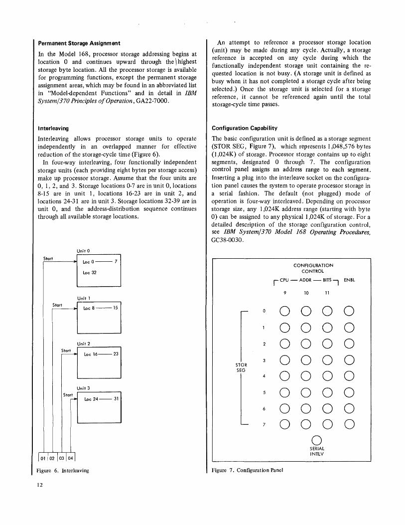
I nte rleav i ng
Interleaving allows processor storage units to operate independently in an overlapped manner for effective reduction of the storage-cycle time (Figure 6).
In four-way interleaving, four functionally independent storage units (each providing eight bytes per storage access) make up processor storage. Assume that the four units are 0, 1, 2, and 3. Storage locations 0-7 are in unit 0, locations 8-15 are in unit 1, locations 16-23 are in unit 2, and locations 24-31 are in unit 3. Storage locations 32-39 are in unit 0, and the address-distribution sequence continues through all available storage locations.
Unit 0
Start l..ocO--7
l..oc 32
Unit 1 Start
l..oc8--15
Unit 2
~ l..oc 16--23
Unit 3 Start
--- l..oc 24-- 31
I 01 I 02 I 03 I 04 I Figure 6. Interleaving
12
An attempt to reference a processor storage location (unit) may be made during any cycle. Actually, a storage reference is accepted on any cycle during which the functionally independent storage unit containing the requested location is not busy. (A storage unit is defined as busy when it has not completed a storage cycle after being selected.) Once the storage unit is selected for a storage reference, it cannot be referenced again until the total storage-cycle time passes.
Configuration Capability
The basic configuration unit is defined as a storage segment (STaR SEG, Figure 7), which represents 1,048,576 bytes (1,024K) of storage. Processor storage contains up to eight segments, designated 0 through 7. The configuration control panel assigns an address range to each segment. Inserting a plug into the interleave socket on the configuration panel causes the system to operate processor storage in a serial fashion. The default (not plugged) mode of operation is four-way interleaved. Depending on processor storage size, any 1,024K address range (starting with byte 0) can be assigned to any physical 1 ,024K of storage. For a detailed description of the storage configuration control, see IBM System/370 Model 168 Operating Procedures, GC38-0030.
CONFI GURA liON CONTROL
I CPU - ADDR - BITS I ENBL
9 10 11
0 0 0 0 0 0 0 0 0
2 0 0 0 0 3 0 0 0 0 STOR
SEG
0 0 0 0 4
5 0 0 0 0 6 0 0 0 0 7 0 0 0 0
0 SERIAL INTLV
Figure 7. Configuration Panel

PROCESSOR STORAGE CONTROL FUNCTION
All storage accesses from the instruction processor and channels are controlled by the processor storage control function (PSCF). Each access transfers one doubleword (eight bytes). Five different logical areas make up the PSCF:
1. High-speed buffer storage and control. 2. Translator. 3. Translation lookaside buffer (TLB). 4. I/O channel control (I/O buffer). 5. Processor storage controls.
Note: The PSCF of the attached processing unit has all the logical areas except the I/O channel buffers. The processor storage controls in the APU are interleaved with the host CPU and are described in Appendix G.
Buffer Storage Control
The buffer storage control handles all storage requests from the instruction processor for data stores or fetches. It also monitors all channel store operations so that the high-speed buffer storage can be invalidated, if necessary.
High-speed Buffer
Buffer storage provides high-speed access to instructions and data. A fetch from the buffer takes less than one-fourth of the time required for the same fetch from processor storage. Buffer action is automatic. Although it holds only a portion of processor storage contents, the objective of the buffer is to contain that area that the program is currently using.
The high-speed buffer holds recently accessed storage data and is constantly being updated. The buffer's standard capacity is 8K in the 3168-1, and 32K in the 3168-3 and APU. Buffer storage is distributed in 32-byte blocks, each block consisting of four doublewords. The 32K buffer of the 3168 -3 or APU is partitioned in to eight blocks per column, with 128 columns, for a total of 1,024 blocks (Figure 8). In the 3168-1, the 8K buffer has four blocks per column, with 64 columns, for a total of 256 blocks. If the buffer of the 3168 is expanded to 16K, it is then partitioned into eight blocks per column and 64 columns, for a total of 512 blocks. Correspondingly, processor storage also is conceptually divided into 64 or 128 columns, the number of blocks per column varying with the size of processor storage.
During operation, a correspondence is set up that relates each block in buffer storage to a block in the corresponding column of processor storage. Each time the instruction processor makes a fetch, buffer storage control determines whether there is an assigned buffer block corresponding to the addressed processor storage block. If none is found, one of the buffer blocks is automatically assigned to the block that was addressed, the block address is placed in the buffer
Adr Bits
20 21-26 27,28
~ -~T Buffer Address Array ~
AAO AA3 AM AA7
i'- -fi-
~o--o[r--D
LJLJ C] M2~ I-f.-.
B63 I"- M40 DO 0
B65
::~*~ __ LJ LJ ___ LJ it I ) Buffer Data Array
: j/
8 or 16K
J
COCI / r-~ C64 C12 7 m I I I
8K Rl I !--f--
I
~ r i--f--
I R3
!--r--J 60[j I--r-- {
'r f\\ R6
I----t---III
R7 ~~ ( ~
=8 or 16K--l I ~~----------32K------------~~
Figure 8. High-speed Buffer Operation
32K
block's address array, and a buffer storage block load is called for. While the block is being execu ted, the address is made invalid until the fetch is complete.
When an instruction processor fetch dictates a block load, four 8-byte (overlapped) accesses to processor storage are required. The first processor storage location selected is the one containing the data addressed. When the location is available, the data is sent directly to the instruction processor and is also loaded into buffer storage. The three remaining (overlapped) processor storage fetches needed to complete the block load are made one at a time on each succeeding cycle, if the required processor storage units are not busy.
For a channel store operation, a check is made to determine whether the referenced data is in the applicable buffer storage; if it is, the buffer storage data is invalidated and processor storage data is updated. If the referenced data is not in the applicable buffer storage, only processor storage is updated. Channel fetch requests are made only to processor storage.
Central Processing Unit 13
Because buffer storages can contain only a portion of processor storage data at one time, any buffer block can be reassigned to any other block of the corresponding column in processor storage. Priority of reassignment is based on usage. Each time data within a buffer block is referenced by
, an instruction processor fetch, that block is logically moved to the top of a logic-controlled activity list. Intervening blocks are logically moved down one position to fill the vacated slot. Note, however, that the logical movement of a block within the list involves no data transfer. When all four (eight in the case of a 16K or 32K buffer) buffer blocks within a column are assigned and the instruction processor makes a fetch request to a corresponding storage location not yet in buffer storage, the buffer block lowest on the activity list is cleared and reassigned to the referenced processor storage block. (The buffer block at the bottom of a particular activity list is the one in that column that has gone the longest without being referenced by an instruction processor fetch.)
Store-type operations always update processor storage, but buffer storage is not updated unless the referenced processor storage block has a corresponding buffer storage block assigned. In summary, store operations do not cause reassignment, loading of a buffer storage block, or changing of the buffer stbrage block activity list.
The 32K buffer is designed for use by the 3168-3 and APU in either basic control mode or extended control mode. When used in extended control mode, 4K paging is required. If a user's system control program requires 2K paging, the buffer defaults to 16K capacity. The buffer is automatically reset to 32K when the system reverts to 4K paging, or it can be reset manually.
Translator
This unit translates logical addresses to real addresses when the system is in DAT mode and during the execution of an LRA instruction. The translator also holds addresses for TLB searches and updates.
Translation Lookaside Buffer (TLB)
In order to reduce the logical-to-real address translation time, once a translation is completed, the real address of a referenced page is stored in a group of register~ called the TLB. Each real address stored in the TLB is identified as belonging to a particular logical address by: 1. The position in the TLB into which it is stored. 2. Storing bits 8-15 of the logical address into the TLB
entry. Thus, the TLB contains up to 128 logical-real address
pairs. Subsequent translations for the same addresses, and their multiple processor storage references, are avoided because the real address required is available immediately from the TLB.
14
TLB Operation
Each logical address supplied by the program causes access to both the high-speed buffer (to examine address of data contained), and the TLB (to determine if real address and protect key are resident).
If the real address is available from TLB, it is compared with addresses read out of the high-speed buffer-address array to determine if the data field required is there (Figure 9). The real address is also used to access processor storage if the operation requires it. If the real address is not available from the TLB, the logical address is translated and the TLB is updated with the newly translated address.
The TLB can be purged with the program by issuing a purge TLB instruction; it can be partially purged by loading con trol registers 0 and 1, or by issuing a load PSW instruction. The TLB may also be purged by using manual controls such as COMPUTER or SYSTEM RESET. For a description of these instructions, see IBM System/370 Principles of Operation, GA22-7000.
Possibilities for Final Resolution:
1. The logical address has been previously translated, and its real address now resides in the TLB. It is possible for the address to be resolved in one machine cycle, and to have the data available on the following cycle.
2. The logical address has not been previously translated, or has been previously translated, but does not currently reside in the TLB; thus, a full translation must take place. Assuming no I/O interference, from 8 to 26 machine cycles are required, depending on the locations of the segment and page table entries required for the translation.
TLB Operation Example: Assume a given logical address is requested by the instruction processor (see Figure 9). Logical address bits 8-20 select the entry line in the TLB. Logical address bits 8-15 are compared against the entry from the TLB. If the TLB compare is unsuccessful, a full translation is performed. Before going to processor storage to do the full translation, a determination is made to see if the required translation entries (or any part of them) are in the buffer. If they are, the translation is made, using the buffer entries. If only part (or none) of the entries is in the buffer, then part (or all) of the translation is made, using processor storage.
If the TLB compare is successful, no translation is required and the real address is transferred from the TLB to the buffer address array to find if the entry is in the buffer. This ultimately determines whether the fetch is made from the buffer or from processor storage.
Logical Address from Instruction Processor I I 8 15 20 21 26 2728 31 '----:--::-v----"'-v---' \....,./
High-speed Buffer
B2
B3
B4
B5
B6
B7
Figure 9. TLB Operation
High-speed Buffer Address Arroys
AA 1 - - - - - - - - - - - - - AA7
08-20
) l J \ \ \ \ I 1 l
Doubleword to Instruction Processor ~
I/O Channel Controls (I/O Buffed
The I/O channel controls (Figure 10) receive and process channel storage requests. Each channel attached to the CPU has a fixed amount of channel control buffer (a buffer group) dedicated to its use. This buffering results in attaining higher channel data rates through maximum utilization of the four~way interleaved processor storage.
A channel buffer group provides two sections, each with control ability and data capaoHy for one doubleword inbound and one doubleword outbound. To transmit information to processor storage during an I/O read operation, the channels place data and control signals on a channel in-bus to the channel buffers in the I/O channel control. Channel buffer priority determines which buffer section may use storage and transmit data via the storage in-bus at any given time. Priority is established at installation time: highest storage priority is assigned to buffer group 1, second highest priority to buffer group 2, etc. The resultant channel-to-channel buffer relationship may be seen on the indicator viewer. As each channel buffer is loaded, it requests use of one of the four interleaved units of processor storage. If the channel is performing a store operation, the high-speed buffer address array is accessed, and if the affected address is resident there, that buffer block is invalidated.
The loading of a channel buffer section frees the channel in-bus for use by other channels vying for its use. Simultaneous multichannel data transfers are increased by use of the channel dual bus function.
Channe I Data Bus-In B
Channel Data Bus-In A
'" Qj c: 5 6
Channel Data Bus-Out A
Channel Data Bus-Out B
Figure 10. I/O Channel Controls
.,..-- ........
/ '\ \ I I I I I
I/o Buffer
\. ./
yone Buffer Group
"--
Central Processing Unit 15
Page of GA22-7010-4 Revised June 18, 1976 By TNL: GN22-0514
Processor Storage Controls
The processor storage controls (Figure 11) handle the storage requests made by the high-speed buffer storage controls and by the I/O channel controls.
Both store and fetch operations are modified by the error checking and correction logic in the storage units. Single-bit parity errors are detected and corrected, and double-bit parity errors are detected.
CPU f'APD-- -- --- ---,
Processor Storage Controls Processor Storage Controls
~
High-speed High-speed I/O Channel Buffer Buffer
Controls Storage Storage
Controls Control.
L~ _______ . ___ .1
Figure 11. Processor Storage Controls
INSTRUCTION UNIT (I-UNIT)
This unit fetches, decodes, and buffers'instructions, calculates addresses, fetches required operands, and issues instructions to the execution unit. In addition, the instruction unit controls those portions of the execution unit required for establishing the initial conditions for instruction execution (such as those used for pre fetched operands and decoded operation codes). This unit can prepare several instructions concurrently, and its operation is overlapped with the execution unit. .
EXECUTION UNIT (E-UNIT)
This unit, controlled by microprograms can execute (in best case conditions) a new instruction during every cycle. Where data results determine the execution sequence, nonmicroprogram control is used.
Local Storage
This unit contains the 16 general registers and four floating-point registers.
Writable Control Storage
This facility (in the execution unit) provides basic control as well as microdiagnostic capability. The control storage consists of a combination of read-only storage (ROS) and writable control storage (WCS), plus associated logic.
16
Internal transfers are parity-checked; a parity error causes a machine check. Control storage stores control information that is used to define the state of the execution unit at any given time.
EXTENDED CONTROL
Extended control (EC) mode provides expanded control for the System/370 facilities, including dynamic address translation and program event recording.
EC mode is implemented with a modified PSW format and with extended permanently assigned areas of processor storage. For the format of the EC PSW, see IBM System/ 370 Principles o/Operation, GA22-7000.
Dynam ic Address Translation
Dynamic address translation (DAT) puts a logical address space (expanded processor storage) of up to 16,384K at the user's disposal, regardless of the actual processor storage size. This logical address space is referred to as "virtual storage." For details, see IBM System/370 Principles 0/ Operation, GA22-7000.
SERVICE PROCESSOR (SVP)
The 3168-3 service processor (a standard feature) is a functionally separate realtime monitor that provides improved serviceability and availability. Operating under control of the stored-program-controlled processor, the SVP continuously records the most recent 32 cycles of 199 bits of processor control information. When a hardware failure (either recoverable or unrecoverable) occurs" the control information and machine logout data are stored on an internal disk file containing as many as 16 trace data records.
The capture of this intermittent and hard error data permits better online error analysis. The potential for long outages may be further reduced by the use of a remote service facility. This is a customer option that allows service personnel to link the processor to a remote maintenance facility.
The SVP features include:
• Local and remote communications through an interface.
• Optional display of data on the 3168-3 console or on a system printer, using a standalone or online test diagnostic program.
• Optional attachment of an IBM 3213 Console Printer to record SVP data. The 3213 integrated printer attachment feature is required.
• Channel interface connection that can be used to route diagnostic data to the host or other processor for recording.
• Internal disk me that can store as many as 16 events (for example, hardware failures).
CHANNELS
The IBM 2860 Selector Channel, the IBM 2870 Byte Multiplexer Channel, and the IBM 2880 Block Multiplexer Channel provide for attachment of I/O devices to the Model 168 system (Figure 13). The channel relieves the instruction processor of communication directly with I/O devices and permits data processing to proceed concurrently with I/O operations.
Two buses (A and B) (see Figure 12) are provided to attach the channels. On the standard system, up to three logical channels or three channel frames may attach to bus A and four to bus B. This dual bus facility provides independent priority logic registers and gating for each bus thereby allowing simultaneous data transfer on the two buses.
A standard, single channel-to-control unit interface provides a uniform method of attaching control units to channels. Data is transferred one byte at a time between the I/O device and the channel. An optional two-byte-wide interface on the 2880 channel provides for attachment of devices with very high data rates. Data transfers between the channel and the PSCF are eight bytes (one doubleword) in parallel for both selector and multiplexer channels.
The extended channels feature permits attachment of up to 12 channels to the Model 168. (See Figure 13; also see "Extended I/O Masking" in IBM System/370 Principles of Operation, GA22-7000.)
Channel Attachment
The system attaches a minimum of one 2860 or one 2870 with the optional selector subchannel feature installed, or one 2880 Block Multiplexer Channel.
Frame and channel attachment statistics are conveniently tabulated in Figure 13.
CPU
~ Channel I Dual Bus Af Channel I ~
Processor Storage PSCF I/o Devices
Dual Bus B Channel I - ~ ~ L
Y Channel I Figure 12. Channel Data Flow
Channel Description
Maximum
Channels Extended Channels Channels per Base Feature Frame
Total Number 7 12 -2860/2870 7 7 -2860 6 6 3 2870 2 2 1 2880 6 11 2 Total Frames 7 7 -
Figure 13. Channel Options
Channel Frame Positions
• Channels assigned priorities 1, 2, 3,9, A, and B must be attached to bus A.
• Channels assigned priorities 4, 5, 6, 7, C, and D must be attached to bus B.
• Channels within the same channel frame must be attached to the same bus.
• Channels with the highest speed devices attached should be positioned closest to the instruction processor on the bus to which th~y are attached.
Data Rate Considerations
An 8.5 Mb/sec aggregate data rate can be maintained on each bus providing a total aggregate capability of approximately 17 Mb/sec. Given this capability, Figure 14 illustrates what device data rates can be sustained at various channel priority positions. Generally, the device type noted in each example implies that any other device type with similar characteristics and the same or slower data rate may also be attached.
Priority
Mb/sec Device Type 1 2 3 4 5 6 7
3.0 2305-1 * ..j ..j .; ..j
1.5 2305-2* ..j ..j ..j ..j .; .;
1.25 3420-8 (3803-2) .; .; .; .; .; ..j ..j
0.8 3330, 3340* ..j ..j ..j ..j ..j
0.8 3420-6 (3803-2) ..j ..j ..j .; ..j
I = device type attachable at indicated priority position.
'* = attachable via 2880 channel only.
Figure 14. Device Data Rates
.; .;
.; .;
9 A B C 0
* ..j ..j
.; .; .;
.; .; .; .; .;
I _ Extended _ I ,... Channels .....,
Feature
Channel Description 17
Twelve priority positions are designated: 1, 2, 3,4. 5, 6, 7, 9, A, B, C, and D." Priority is established by plugging jumpers on matrix cards in the PSCF. Devices with higher data rates should be attached to the higher priority channels.
Negligible or no overrun exposure will exist if these guidelines are followed.
The 2870 channels with 0, 1, or 2 selector subchannels may be attached to any priority position, but generally should be positioned as high as possible. The 2870 channels with more than two selector subchannels should be assigned priority position 1,2,3, or 4.
Indirect Data Addressing
In the implementation of dynamic address translation, CCWs in virtual storage must be translated by the control program before execution. To allow the designation of noncontiguous areas of real storage for contiguous areas of virtual storage, the indirect data addressing (optional feature) is used. For details, see IBM System/370 Principles of Operation, GA22-7000.
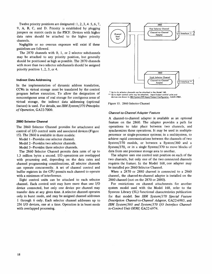
2860 Selector Channel
The 2860 Selector Channel provides for attachment and control of I/O control units and associated devices (Figure 15). The 2860 is available in three models:
Modell-Provides one selector channel. Model 2-Provides two selector channels. Model 3-Provides three selector channels. The 2860 Selector Channel permits data rates of up to
1.3 million bytes a second. I/O operations are overlapped with processing and, depending on the data rates and channel programming considerations, all selector channels can operate concurrently. A set of channel control and buffer registers in the CPU permits each channel to operate with a minimum of in terference.
Eight control units can be attached to each selector channel. Each control unit may have more than one I/O device connected, but only one device per channel may transfer data at any given time. A selector channel operates only in burst mode, and may be assigned channel addresses 1 through 6 only. Each selector channel addresses up to 256 I/O devices, one at a time. Operation is in burst mode with overlapped processing.
18
2860
First Selector Channel
Channel-to-Channel Adapter
2860
Sixth Selector Channel
Chonnel-to-Channel Adapter
* Up to six selector channels can be attached to the Model 168. ** Up to eight control units may be attached. Input/output control units and
devices are shown in IBM System/370 Input/Output Configurator, GA22-7002.
Figure 15. 2860 Selector Channel
Channel-to-Channel Adapter Feature
A channel-to-channel adapter is available as an optional feature on the 2860. The adapter provides a path for operations to take place between two channels, and synchronizes those operations. It may be used in multipleprocessor or single-processor systems; in a multisystem, to achieve rapid communications between the channels of two System/370 models, or between a System/360 and a System/370, or in a single System/370 to move blocks of data from one processor storage area to another.
The adapter uses one control unit position on each of the two channels, but only one of the two connected channels requires the feature. In the Model 168, one adapter may be installed per 2860 Selector Channel.
When a 2870 or 2880 channel is connected to a 2860 channel, the channel-to-channel adapter is installed on the 2860 channel (not on the 2870 or 2880).
For restrictions on channel attachments for another system model used with the Model 168, refer to the Systems Library (SL) functional characteristics publication for that model. See IBM Systt!m/370 Special Feature Description Channel-to-Channel Adapter, GA22-6983, and IBM System/360 and System/370 I/O Interface Channelto-Control Unit OEMI, GA22-6974.

2870 Byte Multiplexer Channel
The 2870 Byte Multiplexer Channel provides for attachment of a wide range of low- to medium-speed I/O control units and associated devices (Figure 16). The basic 2870 Byte Multiplexer Channel (with 192 sub channels) can attach eight control units and address 192 I/O devices, using unit addresses up to BF (hexadecimal). The basic byte multiplexer channel can operate several byte multiplexmode I/O devices concurrently or a single burst-mode device.
Two 2870's can be attached to the Model 168: each one provides 192 sub channels , plus four optional selector sub channels. The address of the first 2870 must be 0; the second 2870 may be assigned any address from 1 through 6.
A selector sub channel can (1) operate one I/O device concurrently with the basic byte multiplexer channel, and (2) permit attachment of eight control units for certain devices having a data rate not exceeding 200 kilobytes (kb) a second. Regardless of the number of control units attached, a maximum of 16 I/O devices can be attached to a selector subchannel.
IBM 2870 Byte Multiplexer Channel"''''
First Selector Subchannel
Second Selector Subchannel
Third Selector Subchannel
Fourth Selector Subchannel
*Up to two 2870s may be attached to the fv4.odel 168.
I/o Interface ***
Addresses up to 1921/0 devices
I/o Interface **'"
Addresses up to 16 I/o devices
I/o Interface ***
Addresses up to 16 I/o devices
I/o Interface *"'*
Addresses up to 16 I/o devices
I/o Interface **'"
Addresses up to 161/0 devices
** A system with the first 2870 may attach up to six selector channels; a system with the first and second 2870 may attach up to five selector channels.
***Up to eight control units may be attached. Input/output control units and devices are shown in the IBM System/370 Input/Output Configu~I GA22-7002.
Figure 16. 2870 Byte Multiplexer Channel
The maximum aggregate data rate for the byte multiplexer channel ranges from 110 kb to '670 kb, depending on the number of subchannels in operation aad the rates of the attached I/O devices. When four selector subchannels are installed in the 2870, the first three may operate at a maximum of 180 kb and the fourth at 100 kb (maximum). When three selector sub channels are installed, all three may operate at 200 kb (maximum). Note that when four subchannels are installed and the first three are operating at 200 kb, the fourth subchannel cannot be operated.
Each selector sub channel in operation diminishes the basic byte multiplexer channel's maximum data rate of 110 kb; the maximum data rates for concurrent selector sub channel operations are:
Basic Byte Multiplexer
Channel (Kilobytes)
110 88 66 44 30
Data Rates for Selector Subchannel (Kilobytes)
1st or 2nd 2870 1st 2870 Only 1st 2nd 3rd 4th
180 180 180 180 180 180 180
180 180 100
For 200-kb selector sub channel operation, these rates prevail:
110 80 200 55 200 200 30 200 200 200
Note: The maximum data rate for 2870 Selector Subchannels pertains to attachment of magnetic tape devices; timing factors other than data rates may preclude attachment of direct-access storage devices that have lesser'data rates. Also, note that when other channels in addition to the 2870 are in operation, the total system I/O data rate must be analyzed.
The maximum data rate for selector subchannels and for the basic byte multiplexer channel is a function of the channel buffer priority assigned to that 2870. (See "Data Rate Considerations" for priority assignment.)
Channel Description 19
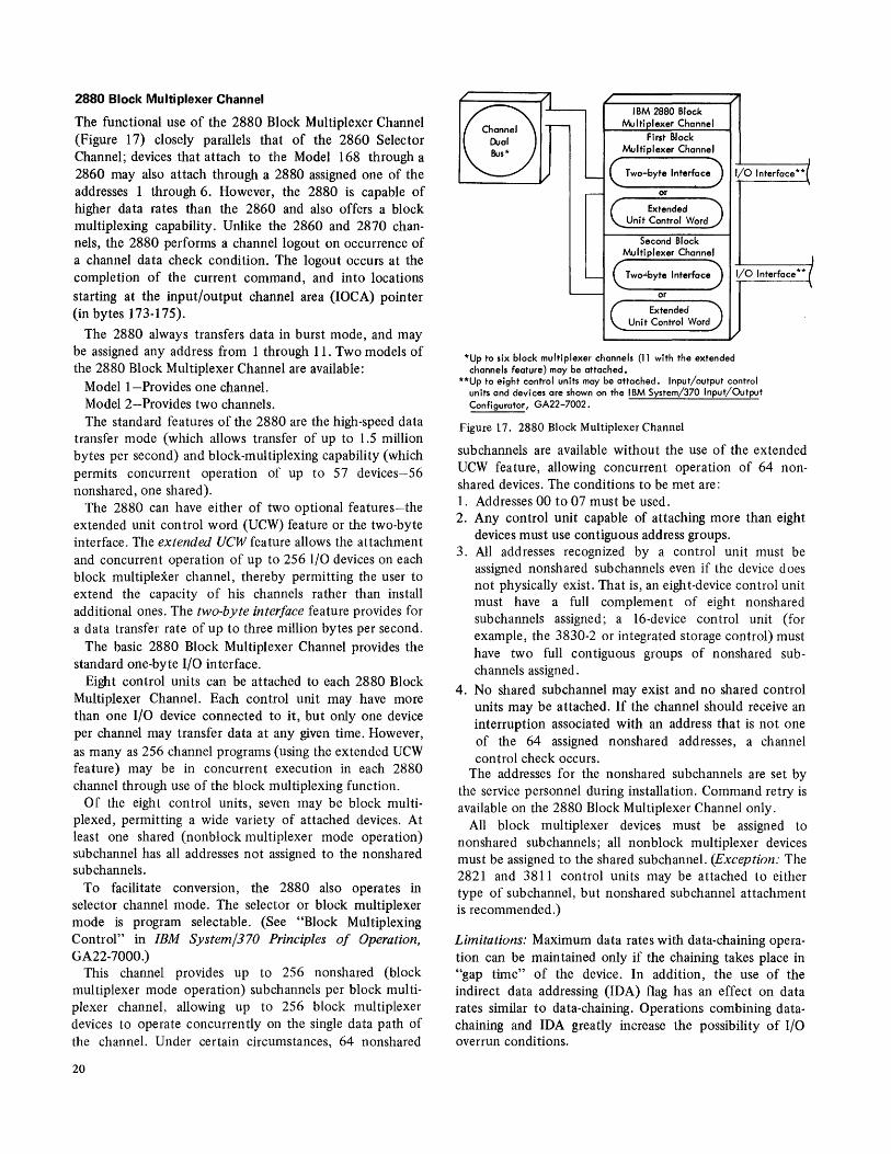
2880 Block Multiplexer Channel
The functional use of the 2880 Block Multiplexer Channel (Figure 17) closely parallels that of the 2860 Selector Channel; devices that attach to the Model 168 through a 2860 may also attach through a 2880 assigned one of the addresses 1 through 6. However, the 2880 is capable of higher data rates than the 2860 and also offers a block multiplexing capability. Unlike the 2860 and 2870 channels, the 2880 performs a channel logout on occurrence of a channel data check condition. The logout occurs at the completion of the current command, and into locations starting at the input/output channel area (IOCA) pointer (in bytes 173-175).
The 2880 always transfers data in burst mode, and may be assigned any address from 1 through 11. Two models of the 2880 Block Multiplexer Channel are available:
Model I-Provides one channel. Model 2-Provides two channels. The standard features of the 2880 are the high-speed data
transfer mode (which allows transfer of up to 1.5 million bytes per second) and block-multiplexing capability (which permits concurrent operation of up to 57 devices-56 nonshared, one shared).
The 2880 can have either of two optional features-the extended unit control word (UCW) feature or the two-byte interface. The extended UCW feature allows the attachment and concurrent operation of up to 256 I/O devices on each block multiplexer channel, thereby permitting the user to extend the capacity of his channels rather than install additional ones. The two-byte interface feature provides for a data transfer rate of up to three million bytes per second.
The basic 2880 Block Multiplexer Channel provides the standard one-byte I/O interface.
Eight control units can be attached to each 2880 Block Multiplexer Channel. Each control unit may have more than one I/O device connected to it, but only one device per channel may transfer data at any given time. However, as many as 256 channel programs (using the extended UCW feature) may be in concurrent execution in each 2880 channel through use of the block multiplexing function.
Of the eight control units, seven may be block multiplexed, permitting a wide variety of attached devices. At least one shared (nonblock multiplexer mode operation) sub channel has all addresses not assigned to the nonshared subchannels.
To facilitate conversion, the 2880 also operates in selector channel mode. The selector or block multiplexer mode is program selectable. (See "Block Multiplexing Control" in IBM System/370 Principles of Operation, GA22-7000.)
This channel provides up to 256 nonshared (block multiplexer mode operation) subchannels per block multiplexer channel, allowing up to 256 block multiplexer devices to operate concurrently on the single data path of the channel. Under certain circumstances, 64 nonshared
20
IBM 2880 Block Multi lexer Channel
First Block Multiplexer Channel
Two-byte Interface
or
Extended Unit Control Word
Second Block Multiplexer Channel
TWO.l.byte Interface
or
Extended Unit Control Word
*Up to six block multiplexer channels (11 with the extended channels feature) may be attached.
**Up to eight control units may be attached. Input/output control units and devices are shown on the IBM System/370 Input/Output Configurator, GA22-7002.
Figure 17. 2880 Block Multiplexer Channel
sub channels are available without the use of the extended UCW feature, allowing concurrent operation of 64 nonshared devices. The conditions to be met are: 1. Addresses 00 to 07 must be used. 2. Any control unit capable of attaching more than eight
devices must use contiguous address groups. 3. All addresses recognized by a control unit must be
assigned nonshared subchannels even if the device does not physically exist. That is, an eight-device control unit must have a full complement of eight nonshared sub channels assigned; a 16-device control unit (for example, the 3830-2 or integrated storage control) must have two full contiguous groups of nonshared subchannels assigned.
4. No shared sub channel may exist and no shared control units may be attached. If the channel should receive an interruption associated with an address that is not one of the 64 assigned nonshared addresses, a channel control check occurs.
The addresses for the nonshared subchannels are set by the service personnel during installation. Command retry is available on the 2880 Block Multiplexer Channel only.
All block multiplexer devices must be assigned to nonshared subchannels; all nonblock multiplexer devices must be assigned to the shared subchannel. (Exception: The 2821 and 3811 control units may be attached to either type of subchannel, but nonshared subchannel attachment is recommended.)
Limitations: Maximum data rates with data-chaining operation can be maintained only if the chaining takes place in "gap time" of the device. In addition, the use of the indirect data addressing (IDA) flag has an effect on data rates similar to data-chaining. Operations combining datachaining and IDA greatly increase the possibility of I/O overrun conditions.

USAGE METERING
Usage meters appear on the following units of the Model 168: the 3066 System Console, the 2860 Selector Channel, the 2870 Byte Multiplexer Channel, the 2880 Block Multiplexer Channel, and the 3068 Multisystem Communication Unit (Model 168 MP). Meters also appear on individual I/O units.
For the 3168 Processing Unit, the customer usage meter and the CE meter are on the main control panel. The CE key switch controls which of these meters is to be run while the system is in operation; that is, initiating, executing, or completing instructions, including I/O and assignable unit operations. The system light indicates when the system is in operation. The test light may indicate when the key switch is in the CE meter position.
The 2860 Selector Channel Models 1-3, the 2870 Byte Multiplexer Channel, and the 2880 Block Multiplexer Channel each have one usage meter mounted on their respective power control panels.
When each meter runs depends on the general function performed by the unit to which it is attached. The function of those units, by category, and the conditions under which the meter runs, are described in Figure 18. (Also see "Usage Meter" under "Multiprocessing Feature" and "Attached Processor Feature.")
System Activity Meter
The system activity monitor displays the average activity of the major system elements on the system activity meter. The meter provides a dynamic visual indication of the instruction processor or I/O activity.
System parameters are selected on a function selector control for meter display, and a monitor hub permits external attachment of a strip chart recorder or time-base counter for precise recording of a selected function. The panel controls provide flexibility in performing simple combinatorial logic for setting up a particular measurement. Among the measurements, which are easily made on a one-at-a-time basis, are the following: 1. Compute time (total, supervisor state, or problem
state). 2. Compute-channel overlap for selected channels. 3. Channel-to-channel overlap for selected channels. 4. Total channel time for selected channels.
Compute measurements can further be made for a specific PSW storage protection key when KEY SEL is enabled.
The calibrate check switch is provided for use in verifying that individual functions within the device are in proper calibration.
Functions
The system activity meter's monitor hub provides for the display and recording of the system activity as well as a selected function. The system activity time signal (pin 1) is active when the system light is on and the manual light is off, that is, when the instruction processor is in either the run or wait state. The 'percent of selected function' signal (pin 3) is active when the selected function is executing, and therefore permits recording of the system activity meter's indication. (It may also be brought to the 100 percent activity level by pressing the calibrate check switch. See "Calibrate Check," in this section.)
The monitor hub is located under the reading board beneath the main control panel; see Figure 19. The three-conductor cable, supplied for connecting a recording device to the hub, provides the following signals:
Connector pin 1 (black) - System activity time output Connector pin 3 (white) - 'Percent of selected function' output Connector pin 2 (green/yellow) - Common signal-return
The recording device must provide a 90-ohm terminating resistor for each of the two signal lines (pins 1, 3) and must offer a total input resistance of 1,000 ohms, minimum.
Calibrate Check: The calibrate check switch is used periodically to ensure that the system activity meter (and/or attached recorder) is properly calibrated. When this switch is pressed to the right, the meter indicates 100 percent if it is in calibration. Simultaneously, the 'percent of selected function' output (pin 3, white) of the monitor hub is at the 100 percent signal level. This 100 percent calibrate signal level is not affected by calibration of the activity meter.
Function: The function select switch is a seven-position rotary switch that selects system functions for display on the system activity meter and for presentation to the monitor hub. All functions are calibrated to give a full-scale meter reading when the selected function is active 100 percent of the time. The function performed for each of the seven switch settings is:
1. I/O-I/O Overlap-This position of the function select switch provides a logical AND between the individual channel function activities selected by the channel select lever switches. For example, if the degree of overlap between the operation of two channels is desired, the channel select lever switches for the two channels are set and the function select switch is set to I/O-I/O OVLP. The system activity meter indicates that portion of time when the selected channels are active simultaneously.
Functions 21
2. I/O-This position of the function select switch causes the function activity of all the channels selected by the channel select lever switches to be displayed. Meter indication includes both the overlapped and unoverlapped I/O activity.
3. I/O Compute-This position of the function select switch provides a logical AND between the I/O function (see item 1) and the compute total function (see item 6).
4. Off-The off position of the function select switch disables the system activity meter.
S. Compute Supervisor-This position of the function select switch causes the meter to display all computing activity of the supervisor state (PSW bit IS equals 0).
6. Compute Total-This position of the function select switch causes all computing activity to be displayed. This indication includes both supervisor and problem state computation. If the CPU is totally compute bound, the meter reading will be 100 percent.
7. Compute Problem-This position of the function select switch causes the meter to display all computing activity of the problem state (PSW bit IS equals 1).
Channel Select: Twelve (O-B) channel select lever switches provide a means for selecting the channel or channels which participate in the I/O or I/O related measurements. When enabled, the channel select switches allow the activity of the respective channels to be displayed on the system activity meter.
Storage Protection PSW Key Select: This 16-position (O-F) rotary select switch is used in conjunction with the gate key switch to select the PSW key under which computing is monitored.
Gate Key: This two-position (OFF and ENBL) key lever switch in the enable position activates the storage protection PSW key select switch. The gate key switch is used with the I/O compute, compute supervisor, compute total, and compute problem positions of the function select switch.
MODEL-DEPENDENT FUNCTIONS
The compatibility rule of System/370 does not apply to a number of machine functions for which neither the frequency of occurrence nor usefulness of results warrants identical action on all models. These functions include both the handling of invalid programs and machine malfunctions.
Whenever model dependency exists, the definition of System/370 allows choice in implementation or specifies that the operation is unpredictable. The intent is that the user should ignore results that are defined as unpredictable and generally should not base his program on any function where choice in implementation is permitted.
22
In some cases where choice in implementation is permitted, models make implementation information available to the program. (Example: The maximum machine-check logout length pro-Tided by the store CPU ID instruction.) The use of this information is necessary by some programs but, in order for the program to run on other models, the information must be used with care.
Considering any particular installation and operation, the operation normally is not truly unpredictable; the action may depend on the particular system components or on the input data. The purpose of this section is to describe how some of the model-dependent functions are performed on the Model 168. It should be noted, however, that, except as described in the preceding paragraph, writing a program on the basis of information contained in this section is in violation of the rules of compatibility of System/370. If a program relies on a function that is model dependent, it may not run on another model of System/370. Even if the program takes into account the model-dependent operation of all other models of System/370, difficulties may be encountered if and when new models of System/370 are introduced. Furthermore, a mandatory engineering change may in some instances require a change in the execution of a model-dependent function in a machine installed in a customer's office, and hence may require changes in a program making use of such model-dependent information.
Logout
Instruction processor logout starts at the processor storage location indicated by CR 15 and extends for 1416 (decimal) bytes. The logout contains the instruction processor working registers, all the indicators on the indicator viewer, and the CRT display.
Machine Check (Switch)
This switch varies in nomenclature throughout the System/ 370, and it is described in System/370 Model 168 Operating Procedures, GC38-0030. Similar functions of this switch in other models include: CHECK CONTROL (Model 135, Model 145, and Model ISS) and MACH CHECK STOP (Model 195).
Hardware Retry
This retry attempts to correct machine errors if sufficient information is available to re-execute the instruction.
Software Retry
This retry attempts to correct some errors that can cause machine checks. No invalid results are computed if correction is not successful.
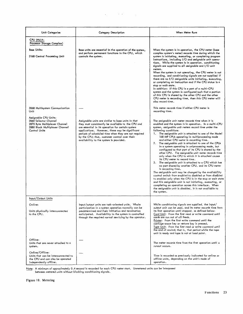
Unit Categories
CPU (PSCF-Processor Storage Complex)
Base Units:
3168 Central Processing Unit
3068 Multisystem Communication Unit
Assignable CPU Units: 2860 Selector Channel 2870 Byte Multiplexer Channel 2880 Block Multiplexer Chonnel Control Units
Input/Output Units
Online:
Units physically interconnected to the CPU.
Offline: Units that are never attached to a system.
Online/Offline: Units that can be interconnected to the CPU and can also be operated independently offl ine.
Category Description
Base units are essential in the operation of the system, and perform permanent functions in the CPU, which controls the system.
Assignable units are similar to base units in that they must consistently be available to the CPU and are essential in its operation for certain system applications. However, there may be significant periods of scheduled time when they are not required by the CPU; thus, customer control over their availability to the system is provided.
Input/output units are task-oriented units. Whole participation in a system operation normally can be predetermined and their initiation and termination anticipated. Availability to the system is controlled through the required normal servicing by the operator.
When Meter Runs
When the system is in operation, the CPU meter (base complex system's meter) records time during which the system is initiating, executing, or completing program instructions, including I/o and assignable unit operations. While the system is in operation, conditioning signals are supplied to all assignable and I/O unit meters. When the system is not operating, the CPU meter is not recording, and conditioning signals are not supplied if there are no I/o assignable units initiating, executing, or completing an instruction and if the CPU status is a stop or wait state. In addition: If this CPU is a part of a multi-CPU system and the system is configured such that a partion of this CPU is shared by the other CPU and the other CPU mefer is recording time, then this CPU meter will also record time.
This meter records time if either CPU meter is recordi ng ti me.
The assignable unit meter records time when it is enabled and the system is in operation. In a multi-CPU system, assignable unit meters record time under the following conditions: 1. The assignable unit is ottached to one of the Model
168 MP CPUs operating in multiprocessing mode and either CPU meter is recording time.
2. The assignable unit is attached to one of the CPUs in a system operating in uniprocessing mode, but configured so that part of its CPU is shared by the other CPU. The assignable unit meter records time only when the CPU to which it is attached causes its CPU meter to record time.
3. The assignable unit is attached to a CPU which has no part shared by another CPU, and its CPU meter is recording time.
The assignable unit may be changed by the availability control switch from enabled to disabled or from disabled to enabled only when the CPU is in the stop or wait state and this assignable unit is not initiating, executing, or completing an operation across this interface. When the assignable unit is disabled, it is not avai lable to the system.
While conditioning signals are supplied, the input/ output unit can be used, and its meter records time from its first operation until stopped, as defined below: Card Unit: From the first read or write command until cards are run out of all feeds. Printer: From the first write command until the carriage space key or restore key is pressed. Tape Unit: From the first read or write command until the end of rewind; that is, that period while the tape unit is ready and tape is not at load point.
The meter records time from the first operation until a runout occurs.
Time is recorded as previously indicated for online or offline units, depending on the unit's mode of operation.
Note: A minimum of approximately 0.4 second is recorded for each CPU meter start. Un metered units can be interposed between metered units without blocking conditioning signals.
Figure 18. Metering
Functions 23

DETAILS OF MACHINE CHECKS
The illustrations and tables on this page are taken (for this model) from the IBM System/370 Principles of Operation, GA22-7000. They are reproduced here for reference only.
Machine-check Condition Masking
Action when Disabled for
Subclass Condition Mask Subclass Condition
Hardstop Hardstop' Bit = 0 Bit = 1
SD System Damage B P* Check Stop CD Time-of-Day Clock Damage B and EM P* P* SR System Recovery Band RM D D ED External Damage B and EM P* P*
Action Code Definition
P Indication held pending.
D Indication may be held pending or may be discarded.
* System integrity is undependable.
B PSW bit 13.
Machine-check Control Register Bits
Bit On System Bit Description (CR14) Position Reset Bit =
CS Check Stop Orl 0 1
SL Sync Mach Chk Ext Log Orl 1 1
IL I/o Ext Log Orl 2 0 ... _--
RM Recovery Report Mask 4 0 -------.---1------
DM Degradation Report Mask 5 0
EM External Damage Report Mask 6 1
WM Warning Mask 7 0 -------------1--
AL Async Mach Chk Ext Log Or! 8 0
FL Async Fixed Log Orl 9 0
Control Register 14
24
Control Register 15
Machine-check Extended Logout Pointer
29 31
Bits 8-28 of control register 15, with three low-order zeros appended, specify the starting location of the machinecheck extended logout area. Bits 0-7 and 29-31 are reserved. The contents of control register 15 are set to 512 (decimal) by system reset.
Allocation of Control Register Fields
01 Reg FUNCTION No.
0 System Control Translate Control I External Interruption Masks
1 Segm Tbl Length Segment Table Origin Address I 2 Channel Masks
3
4
5
6
7
8 I Monitor Masks
9 RER Control I PER GR Alteration Masks
10 PER Starting Address
11 PER Ending Address
12
13
14 Error Recovery Control I 15 MCEL Address
Permanent Storage Assignment (Partial List)
Address (Dec)
176-215 216-223 224-231 232-239 240-247 248 249-251 252-255 256-351 352-511
Purpose
Unused CPU timer logout area Clock comparator logout area Machine-check interruption code Unused O's Failing-storage address Unused Asynchronous fixed logout Register save area

Machine-check Interruption for Model 168
loc 232 (Dec)
CR Control registers* D Delayed FA Failing-storage address* FP Floating-point registers*
Machine Check Extended logout length
LG Logout* MS PSW masks and key* PM Program masks and CC* SC Storage error corrected
63
GR General registers* SE Storage error uncorrected IA Instruction address* ST Storage logical validity* KE Key in storage error WP PSWEMWP*
corrected *
Legend: * = stored valid
Bits
0-5 15 16-18 20-23,27-30 1,3,6-14, 19, } 24-26,31-47
Meaning
Subclass Time of interruption occurrence Storage errors Validity
Not assigned; stored as zero
Storage Check: When operating in the diagnostic mode, this provides checks for odd parity on a byte basis. In the ECC mode, it checks for and indicates all double-bit errors. Invalid data is not allowed to enter storage.
Indicators Unique With This Model
These are fixed indicators in the top row of the indicator viewer, under LOGIC CHECKS:
CNSL FILE indicates machine check; if this occurs during power-on sequence, it is necessary to repeat the power-on procedure.
STOR indicates storage failure; this requires configuration procedures.
CON FIG indicates improper storage configuration; this requires reconfiguration.
Indicate Check Stop State
The indicate check stop state is a condition when the manual, system, load, and wait lights are all off with one or Inore "gross error" red lights lit in row A of the indicator viewer. There is no individual check stop indicator.
Store and Display
The store-and-display function permits manual intervention in the progress of a program. The storing and/or displaying of data may be provided by a supervisor program in conjunction with appropriate I/O equipment and the interrupt key.
The operator stores and displays at the operator's console when the instruction processor is in the stopped state. Procedur~s are described in IBM System/370 Model 168 Operating Procedures, GC38-0030.
Machine checks occurring during store-and-display operations do not log immediately, but create a pending log condition that can be removed by a system, CPU, or check reset. The error condition, when not disabled, forces a logout and a subsequent machine-check interruption when the instruction processor is returned to the operating state.
Functions 2S

SYSTEM CONSOLE WITH CRT DISPLAY
The system console (Figure 19) includes the document viewer, storage configuration control panel, console file, indicator viewer, CRT display, main control panel, and operator's console. Additional information concerning these panels and units can be found in the IBM System/370 Model 168 Operating Procedures, GC38-0030.
Document Viewer: Provides a screen for projection of microfilm-format documents. See IBM Operator's Manual, 9921-9922 Document Viewer, S270-0051.
Figure 19. System Console
26
Storage Configuration Control Panel
Storage Configuration Control: Permits manual reconfiguration of storage.
Console File: A read-only, single-drive disk storage unit.
Indicator Viewer: Shows status of controls and registers.
CRT Display: Graphic display of storage, data, and machine status.
Main Control Panel Controls and Indicators: Abbreviated in tabular form in "Appendix B. Controls and Indicators."
Display Console
Main Control Panel
()per~~or Control Panel

Operator's Console
The operator's console is a standard facility on the Model 168 system console. The operator's console (OC) is a program-controlled I/O device that provides: • A keyboard that permits the operator to enter data into
the system.
• A buffer for storing data received from the CPU or data entered via the keyboard. Data stored in the buffer is continuouslydisplayed on the CRT display.
• A display position indicator (cursor), which is displayed on the CRT.
• An audio-visual alarm for alerting the operator.
• A means by which the operator can present attention status to the system.
By means of the CRT mode select switch, the data path to
I the display can be switched between the OC buffer and an instruction processor. The switch is manually operated and has two positions, OP and CEo In the OP position, data flow to the display is from the OC buffer. In the CE position,
I data flow is from an instruction processor. The operator's console operates as a control unit on the
channel (I/O) interface on either a selector or multiplexer channel. Operations with a multiplexer channel are in control unit forced burst mode; that is, the OC forces burst mode for as many as four bytes.
The operation of the operator's console is described in System/370 Model 168 Operating Procedures, GC38-0030.
Operations
This section provides an overview of the various commands and operations that can be performed by the Oc.
Addressing
The OC occupies the position of a control unit on the interface and uses standard IBM System/370 addressing and selection sequences. The OC is addressed by an eight-bit address byte of a preassigned configuration and must be adapted at time of installation to respond only to its assigned address.
Positions on the screen are addressed 0-79 horizontally and 0-34 vertically.
Commands
Eleven different commands can be used by the channel program to control OC operations.
Code
Command Hex Binary Bits 00-07
Test I/O 00 00000000 Write 01 00000001 Set Cursor OF 00001111 Set Buffer Address 27 00100111 Read 06 00000110 Read Manual Input OE 00001110 Sense (Basic) 04 00000100 NoOp 03 00000011 Set Audible Alarm OB 00001011 Lock Keyboard 67 01100111 Erase 07 00000111
Test I/O:
• Transfers pending status at the OC to the channel.
• Ends with the termination of initial selection.
Write:
• OC requests data, and channel responds by sending write data serially to ~C, one byte per service cycle.
• If the OC is attached to a byte multiplexer channel, operations are in control unit forced burst mode; at the end of each four-byte burst, OC disconnects from the channel, then requests selection for transfer of another burst.
• Conunand is concluded by either a channel stop sequence (channel byte count decrements to 0) or an interface disconnect.
Set Cursor:
• Allows display of cursor at new position.
• Unlocks keyboard to allow character entry.
• OC accepts two bytes of data from the channel, one byte per service cycle, and loads them.
Set Buffer Address:
• Places new address in buffer address hold register (BAHR).
• OC accepts two bytes of data from channel, one per service cycle, and loads them.
• Initiates ending status transfer.
Functions 27
Read:
• Blocks display regeneration.
• Data is read from successive buffer locations, and is transferred to channel.
• Operation with multiplexer channel is in four-byte burst mode.
• Execution of read command is terminated when (1) cursor address is same as buffer address of byte being read (buffer and cursor compare), (2) channel signals "stop," or (3) channel issues an interface disconnect.
ReadMI:
• Does not affect display regeneration.
• Three information bytes are transferred to channel, one per service cycle.
• Command termination is initiated by command execution timing logic when load count reaches 2 (indicating the third byte is being sent).
• Channel can terminate command early by initiating interface disconnect or stop sequence.
Sense:
• Transfers two bytes to channel.
• Contents of sense register are transferred in first sense byte.
• Second sense byte contains all O's.
• Sense register is reset and channel end and device end status is set after the two bytes are transferred.
NoOp:
• Immediate-type command.
• Performs no operation at display.
• Allows programmer to tie up I/O unit.
• Causes channel end and device end status to be sent to channel.
Set Audible Alarm:
• Immediate-type command.
• Sounds audible alarm for approximately 1 second and lights attention reset pushbutton/indicator on operator's control panel.
• Causes channel end and device end status to be sent to channel.
28
Lock Keyboard:
• Immediate-type command.
• Locks keyboard and inhibits display of cursor.
• Causes channel end and device end status to be sent to channel.
• Set cursor command used to unlock keyboard and allow display of cursor.
Erase:
• Places blank code in each buffer location.
• Locks keyboard and removes cursor.
• Resets buffer address, cursor, and keyboard logic.
• Display regeneration is inhibited until after buffer is erased; however, nothing is displayed at that time.
• If OC is attached to multiplexer channel, channel end is set in initial status byte, and OC disconnects from channel; OC performs control-unit-initiated selection sequence to send ending status, which contains only device end.
• Erase operation is completed when space code is stored in last buffer location.
Resets
Interface Disconnect: A halt I/O instruction disconnects the OC from the channel and terminates the current operation.
Interface disconnect does not stop buffer and display regeneration.
System Reset: System reset resets the OC sense and control registers, etc., and erases all data from the buffer. The cursor is displayed in the first display position, and the keyboard is unlocked.
Selective Reset: Selective reset affects the OC in the same manner as system reset.
Indicators
Status: Five indicators which reflect the contents of the status register: 1. ATN (attention). 2. BUSY. 3. CH END (channel end). 4. DEV END (device end). 5. UNIT CHK (unit check).
Sense: These indicators reflect the contents of the sense register.

Status Byte
The status byte is used to relate to the channel the current status of the OC~ for example, it may indicate the detection of an error, that the OC is busy, or that it is ready to accept a command, etc.
The status byte is transmitted to the channel: 1. During a channel-initiated selection. 2. To present channel end and accompanying status to the
channel on termination of data transmission. 3. To present device end and accompanying status to the
channel. 4. To present stacked status. 5. To present externally initiated or asynchronous status to
the channel.
Status Bit Meaning
00 Attention-used with unit check to indicate an asynchronous check. Alone, indicates that enter or cancel key was pressed.
01 Not Used 02 Not Used 03 Busy 04 Channel End 05 Device End 06 Unit Check, 07 Not Used
Sense Byte
Two OC sense bytes are transferred to the channel in response to a sense command. The sense bytes record and provide the channel with information regarding unusual conditions that occurred during the preceding operation. The sense bytes are reset by any command other than test I/O, sense, or no op.
Sense Byte 0 Bit
00 01 02 03 04 05 06 07
Byte 1
Meaning
Command Reject Not Used Bus Out Check Equipment Check Data Check Not Used Buffer Address Check Not Used
Not Defined
Synchronous Checks
Synchronous checks are errors which are detected when the OC is engaged in an I/O operation and which are caused by the operation.
Invalid commands and command bytes of incorrect parity are synchronous checks which terminate the operation and are reported (unit check) at initial-selection status time.
Synchronous checks that are repeated at ending status time and do not terminate the operation are: 1. Detection of an invalid address during execution of a set
buffer address or set cursor command. 2. Detection of a data byte of incorrect parity on bus out. 3. Detection of a data byte of incorrect parity on bus in. 4. Detection of an internal buffer address byte of incorrect
parity.
Asynchronous Checks
Asynchronous checks are detected errors that are not related to the current I/O operation.
Asynchronous checks that are detected during an operation are reported on termination of the operation (unless command chaining is indicated) by causing an attention interruption.
Asynchronous checks that occur when the OC is not performing an I/O operation cause an attention interruption immediately. Interlocking inhibits additional interruptions until the next active command is initiated or until the sense data pertinent to the check has been read.
The following are asynchronous checks: 1. Keyboard data parity error. 2. Invalid keyboard address. 3. Invalid buffer address. 4. Buffer data parity error. 5. Buffer address parity error.
Interruptions
The two types of interruptions, normal and error, are described in the following paragraphs.
Normal I nterruptions
The following are interruptions that can occur during normal operation: 1. Channel end and device end status signifies command
completion and that no detectable errors occurred during the operation.
2. Attention status indicates that the enter or cancel key has been pressed. Attention status is program-interpreted to mean that a manual input message is waiting to be transferred from the OC buffer to the channel.
Functions 29
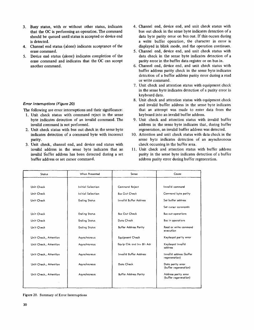
3. Busy status, with or without other status, indicates that the OC is performing an operation. The command should be queued until status is accepted or -device end is detected.
4. Channel end status (alone) indicates acceptance of the erase command.
s. Device end status (alone) indicates completion of the erase command and indicates that the OC can accept another command.
Error Interruptions (Figure 20)
The ·following are error interruptions and their significance: 1. Unit check status with command reject in the sense
byte indicates detection of an invalid command. The invalid command is not performed.
2. Unit check status with bus out check in the sense byte indicates detection of a command byte with incorrect parity.
3. Unit check, channel end, and device end status with invalid address in the sense byte indicates that an invalid Duffer address has been detected during a set buffer address or set cursor command.
Status When Presented
4. Channel end, device end, and unit check status with bus out check in the sense byte indicates detection of a data byte parity error on bus out. If this occurs during a write buffer operation, the character in error is displayed in blink mode, and the operation continues.
s. Channel end, device end, and unit check status with data check in the sense byte indicates detection of a parity error in the buffer data register or on bus in.
6. Channel end, device end, and unit check status with buffer address parity check in the sense byte indicates detection of a buffer address parity error during a read or write command.
7. Unit check and attention status with equipment check in the sense byte indicates detection of a parity error in keyboard data.
8. Unit check and attention status with equipment check and invalid buffer address in the sense byte indicates that an attempt was made to enter data from the keyboard into an invalid buffer address.
9. Unit check and attention status with invalid buffer address in the sense byte indicates that, during buffer regeneration, an invalid buffer address was detected.
10. Attention and unit check status with data check in the sense byte indicates detection of an asynchronous check occurring in the buffer area.
11. Unit check and attention status with buffer address parity in the sense byte indicates detection of a buffer address parity error during buffer regeneration.
Sense Cause
Unit Check Initial Selection Command Reject Invalid command
Unit Check Initial Selection Bus Out Check Command byte parity
Unit Check End i ng Status Invalid Buffer Address Set buffer address
Set cursor commands
Unit Check End i ng Status Bus Out Check Bus out operations
Unit Check End i ng Status Data Check Bus in operations
Unit Check Ending Status Buffer Address Parity Read or write command execution
Unit Check, Attention Asynchronous Equipment Check Keyboard parity error
Unit Check, Attention Asynchronous Equip Chk and Inv Bfr Adr Keyboard invalid address
Unit Check, Attention Asynchronous I nval id Buffer Address Invalid address (buffer regeneration)
Unit Check, Attention Asynchronous Data Check Data pari ty error (buffer regeneration)
Unit Check, Attention Asynchronous Buffer Address Parity Address parity error (buffer regeneration)
Figure 20. Summary of Error Interruptions
30
All System/370 publications are abstracted and listed by order number in IBM System/370 Bibliography, GC20-0001.
Following is a partial list of Model 168 related publications.
General
GA22-6845
GA22-6983
GA22-7000 GA22-7001 GA22-7002
GA22-7010
GA22-7014
GC20-1684
GC38-0030
SY22-6936
IBM System/360 and System/370 Direct Control and External Interruption Features,OEMI IBM System/370 Special Feature Channel-to-Channel Adapter
IBM System/370 Principles of Operation IBM System/370 System Summary IBM System/370 Input/Output Configurator IBM System/370 Model 168 Functional Characteristics IBM System/370 Model 168 Configurator
Introduction to IBM Data Processing Systems
IBM System/370 Model 168 Operating Procedures IBM System/370 Model 168 Theory of Operation/Diagrams Manual (Volume 6)
IBM Operating System (OS/VS)
GC38-0110 Operator's Library: OS/VSl Reference GC38-0120 Operator's Library: OS/VS Console Con
GC38-0210 GC38-0220 GC38-0245
GC38-0255
GC38-0260
GC38-0305
figurations Operator's Library: OS/VS2 Reference Operator's Library: OS/VS2 TSO Operator's Library: System/370 and OS/ VS Handbook Operator's Library: OS/VSl Display Consoles Operator's Library: OS/VS2 Display Consoles Operator's Library: OS/VS TCAM
GC38-0330
GC38-0335
Appendix A. Bibliography
Operator's Library: OS/VS Remote Entry System Operator's Library: OS/VSl CRJE
Representative I/O Devices
Note: References to publications related to specific I/O devices that may be used with this system can be found in IBM System/370 Bibliography, GC20-000 1.
Following is a partial list of publications relating to I/O devices that can be attached to a Model 168:
GA22-6918
GA24-3543
GA26-1589
GA26-1592
GA26-1615
GA26-3599
GA27-2706
GA27-2749
GA27-3051
GA32-0007
GA32-0020
Component Description Bulletin, IBM 2420 Model 7 Magnetic Tape Unit IBM 3211 Printer, 3216 Interchangeable Train Cartridge, and 3811 Printer Control Unit Component Description and Operator's Guide Systems Manual, Reference Manual for IBM 2835 Storage Control and IBM 2305 Fixed Head Storage Module Systems Manual, Reference Manual for IBM 3830 Storage Control Model 1 and 3330 Disk Storage Reference Manual for IBM 3330 Series Disk Storage IBM System/360 Component Descriptions-2314 Direct Access Storage Facility and 2844 Auxiliary Storage Control Original Equipment Manufacturer's Information, IBM 7770 Model 3 Audio Response Unit IBM 3270 Information Display System Component Description Introduction to the IBM 3704 and 3705 Communications Controller Componen t Description: IBM 2420 Model 5 Magnetic Tape Unit IBM 3803 Modell; IBM 3420 Models 3, 5, and 7 Magnetic Tape Subsystem Component Description
Appendix A. Bibliography 31

Page of GA22-70104 Revised June 18, 1976 By TNL: GN22-0514
Appendix B. Controls and Indicators
The normal position for rotary switches is straight up; the normal position for lever switches is straight out. The term CE, as used in these tables, indicates service personnel.
Figure 21 shows the system control panel.
Panel Switch/Indicator Name Type
Al CRT 8RIGHT Potentiometer
CHANNel SELECT Lever Swi tch
STOR PROT PSW KEY SEL Rotary Swi tch
CALl8RATE CHECK Lever Switch
FUNCTION Rotary Swi tch
GATE KEY Lever Switch
Function
Op control: potentiometer, adjusts CRT display. Normally at any setting providing efficient brightness.
Op control: selects channel for activity monitoring. Normally at center position.
Op control: select' storage protect key area for monitoring. May be lert at any setting.
CE/op control: spring-loaded switch calibrates meter (full scale).
Op control: selects function for activity monitoring. Normally off.
Op control: enables STOR PROT PSW KEY SEL. Normally off. 1------ ---------------.-------+--.. ---.----.-----!---------------------------1
A2
A4
MFCHE ROW SELECT
FILE SECTION SELECT
EMERGENCY PULL
Microfiche Switches
Usage meter changeover switch'
CONTROL STORAGE ADDRESS
VOLUME
ADDRESS COMPARE/SYNC
Real CPU CPU/CHAN CHAN
Lagical CPU IC
CS/MS (stap-on-compore)
Positions: CS CSIMS MS
NORM/STOP'
Positions: --r::iORM
STOP
RETRY'
Positions:
LOOP
NORM
DS8L
ECC·
BUFFER'
OVERLAP'
RETRY 8UFFER
'Test light on if switch is not at normal setting.
32
Rotary Switch
Rotary Swi tch
Pull Switch
Lever Swi tches (7)
Rotary Switches (3)
Rotary Swi tch
Rotary Switch
Lever Switch
Lever Switch
Lever Switch
Lever Swi tch
Lever Switch
Lever Swi tch
Lever Swi tch
CE use only.
Combined CE/op control: used in default procedure in power-on sequence. May be left at any setting.
Op control: initiates emergency off in the system; can be reset only by CEo Normally in.
CE use only.
CE use only. Determines which elapsed time meter is to be used to record time. Normally in customer usage meter position.
CE use only. May be left at any setting.
Op control: controls loudness of operator console (attention) audible alarm. May be lert at any setting.
Combination CE/op control: stop. all instruction processors if stop-an-cam pore lever switches are down. May be left at any setting.
Stop on address selected by CPU or APU. Stop on address selected by CPU, APU, or channel. Stop on address selected by channel.
Stop on address selected by CPU or APU. Stop on address selected by IC in either CPU or APU. Op control: when set up or down, causes all instruction processors to stop on mode selected by ADDRESS COMPARE/SYNC (when NORM/STOP switch is set down).
Control storage stop. Normal pmitionj inactive. Main storage stop.
Op control: set down for compore stop. Normally centered.
Norm?' position; inactive. In conjunction with ADDRESS COMPARE/SYNC, causes compare stop.
CE use only.
CE use only.
Normally at center position.
CE use only.
CE use only. Normally at center position.
CE use only. Normally at center position.
CE use only. Normally at center position.
CE us. only. Spring-loaded to return to center position.

Panel
A4 (Cant)
Switch/Indicator Name
SOFT MCH CHK IRPT*
MACHINE CHECK'
STOP ON CHK (up)
PROC (center)
DS8L (down)
DLAT/STOK
CRT MODE SELECT
CE
OP
ATTENTION RESET
WCS/ROS TEST"
WCS/ROS Test Lever
MICRODIAGNOSTICS (3)
LOOP TEST'
LOOP SECT'
RSDT/NON RSDT
STO/DPL Y P8 CTRL'
REPEAT INSN'
INTERVAL TIMER'
FORCED REPEAT'
CS SEL
Type
Lever Switch
Lever Swi tch
Lever Switch
Lever Switch
Function
CombiMd Cf/op control: when down, disable. saft machine check interruption requesto, and blocks soft logout for .ingle .torage errors and intercepted channel errors. Normally at center position.
Combined CE/op control: check. erron.
CPU or APU hardotops on machine; no logout.
Machin~check stop logout (normal po.ilion).
CE u.e only.
CE u.e only.
Combined CE/op control: selects CRT display mode.
CPU or APU and ih internal registers.
Operator communication. display (normal setting).
'-
Pushbutton Op control: turns off (reseh) the backlight that come. on with the alarm.
Rotary Switch
Lever Switch
CE use only. Normally at center position.
CE use only. Normally at center position.
Lever Switch CE use only. Normally at center position,
Lever Switch CE use only. Normally at center position.
Lever Switch Combined CE/op control: used In default procedure in power-on s,quence. Normally at center position.
lever Switch CE use only, Normally at center position.
lever Switch CE use only. Normally at center position.
lever Switch Combined CE/op control disables timer. Normally at center position.
lever Switches (2) CE use only. Normally at center position.
Lever Switch CE use only.
~--~------------------------~-------------+-----------------------------------------AS MANUAL ENTRY SelECT lever Switch
MCDR
MCAR
MRAR
Data Keys" Keys (16)
¢ (cursor advance)" Key
STORAGE SelECT Rot'lry Swi tch
Po.itions:
GEN PUR
FLOAT POINT
MAIN STOR
CHAN 8FR
ADR ARRAY
'Test light on if .witch h not at norm'll setting. "Under control of the SELECT .witch on the A6 panel for 3168-3 with APU.
Op cont.rol: selects register for data entry, causing cursor display with register on CRT.
M'lintenance control data register.
Maintenance control address register (normal pasitlon).
M.aintenance comporand address register.
Op control: enter data into MCDR and addresses into MCAR --one hex digit at·a time.
Op control: advances CRT cursor one byte each time pressed; held in, advances cursor continuau.ly.
Op conlrol: .elects storage area for slore/di.play, Any position.
General registers.
Floating-point regi.ters.
Moin storage.
CE u.e only.
CE use only.
Page ofGA22-70104 Revised June 18, 1976 By TNL: GN22-OS14
Appendix B. Controls and Indicators 33

Page of GA22-70 1 0-4 Revised June 18, 1976 By TNL: GN22-0514
Panel Switch/Indicator Name
A5(Cont) RATE*
~:
MPLE STEP
INSN STEP
PROCESS
SINGLE CYCLE
SINGLE CYCLE REPEAT
START"
SYSTEM RESET
COMPUTER RESET"
COOLING RES ALARM/CHANNEL DELETED
CHECK RESET"
LOAD MD'"
TSLT ADR & DISPLAY MAIN"
ENABLE SYSTEM CLEAR
STORE STATUS"
LOG OUT"
LOAD I BFR"
DIAGN RESTART"
START RIPPLE"
SET IC"
SET PSW"
CS TRANSFER"
RESTART ,.
STOP"
DISPLAY"
STORE .,
ADV ADDRESS ••
POWER ON
TOO CLOCK
POWER OFF
LOAD UNIT
INTERRUPT .,
SYSTEM
MANUAL ••
WAIT"
TEST
LOAD
LOAD'"
'Test light on if switch is nat at normal setting.
Type
Rotary Switch
Pushbutton
Pushbutton
Pushbutton
Pushbutton
Pushbutton
Pushbutton
Pushbutton
Pushbutton
Pushbution
Pushbutton
Pushbutton
Pushbutton
Pushbutton
Pushbutton
Pushbutton
Pushbutton
Pushbutton
Pushbutton
Pushbutton
Pushbutton
Pushbutton
Pushbutton/! ndl cator
Lever Switch
Pushbutton
Rotary Switches (3)
Pushbutton
Indicator
Indicator
Indicator
Indicator
Indicator
Pushbutton
"Under control of the SELECT ,witch on the A6 panel for 3168-3 with APU. "'Under control of the MAINTENANCE switch an the A6 panel for 3168-3 with APU.
34
function
Op control: used to set instruction mode.
CE use only.
CPU or APU executes one machine instruction each time START is pressed.
(Normal position.) Does nat affect CPU or APU operation; CPU and APU operate at narmal clock speed.
CPU and APU operate at normal clock speed. CPU or APU advances by minimum clock amount each time START is pressed. All CPU and APU operations are as in PROCESS position.
CE use only.
Op control: storts the CPU or APU operating in the mode selected by the setting of RATE.
Op control: resets online channel., control units, CPU controls, and APU controls (Including machine checks) to their initial stote.
Op control: resets CPU or APU check indicators, stops CPU or APU, and activotes check reset.
Pres, to stop alann. Notify CEo
Op control: resets CPU or APU, storoge error checks; condition forced by system relet.
Combined CE/op switch: used In default procedure in power-on sequence.
Replace, logical oddre5S with real addre .. in MCAR; location displayed In MCDR. Contents of MCAR and MCDR are set to 0 for Invalid addresses.
Op control: used in conjunction with SYSTEM RESET and IPL to clear registers and storage.
Combined CE/op switch; press after STOP to store status.
Combined CE/op control: causes logout of machine status into main storage starting at location 256 (hex 100).
CE use only.
CE use only.
CE use only.
Op control: sets IC from MCDR.
Op control: sets PSW from MCDR.
CE use only or for emulate.
Op control: loads PSW from location 0; stCl'!5 processing.
Op control: terminates CPU or APU operotion •
Op control: displays dota specified on the CRT.
Op control: enters dota Into storoge.
Op control: advances MCAR address by one doubleword.
Op control: initiates power-on sequence in the CPU, APU, and in selected system units; it is backlighted.
Op control: permits the setting of CPU or APU TOO clock. Nonnally in SECURE position (.pring loaded).
Op control: initiotes power-off .equence in the CPU, APU, and in .elected system units.
Op control: these three .wltches select the I/O units used by a load operation. (May be left at. any setting.)
Op contral: causes an external interruption In the system and sets bit 25 of the Interruption code to a I.
Op light: indicates that a CPU or APU elapsed-time meter is running.
Op light: indicate. thot the CPU or APU is in the stopped .tote.
Op light: indicates thot the CPU or APU is in the wait .tote.
Op light: indicates thot a switch on panel A2, A4, AS, or A6 is nat in the narmal operotlng position.
Op light: indicates that a CPU or APU lood operotion is in progress. A successful load turn. off the indlcotor.
Op control: resets the system and starts a load operation.

Panel Switch/Indicator Name Type
A6 MULTISYSTEM FUNCTION Rat ... y Switch (MP)
---A6 RESIDENT DIAG Lever Switch (3168-3 with APU)
SAM Lever Switch
Positions:
CPU/APU
NORM··
CPU&APU
MAINTENANCE Lever Switch
~ CPU·
NORM
APU·
SELECT Lever Switch
~ CPU
APU
"Test light an If switch Is not at normal setting. ··Under control of the SELECT switch on the A6 ponel for 3168.:.3 with APU.
···Under control of the MAINTENANCE switch on the A6 pon.1 for 3168-3 with APU.
--~--Function
_ .. _---Op control: permits CPU activity to be displayed on the adlacent multisystem activity meter (MSAM).
1-------CE use only.
Combined CE/op control of system activity meter.
Couses a lagical OR of CPU and APU activity to be displayed on the system activity meter.
System activity meter display is under control of the SelECT switch.
Causes a laglcal AN D of CPU and APU activity to be displayed on the system activity meter.
Combined CE/op control. (Switches on ponel AS marked with ... are under control of this switch.)
CPU hOI control of chonnels. Used to run diagnostic telts on CPU.
CPU hOI control of chonnels. Normally at center position.
APU hOI control of channels. Used to run diagnostic: tests on APU.
Combined CI;/op control. (Switches on pone I AS m...ked with •• are dedicated to the Instruction processor selected by this switch.)
CPU is displayed on CRT and microfiche image.
APU is displayed on CRT and microfiche image.
Page ofGA22·7010-4 Revised June 18. 1976 By TNL: GN22-OS14
Appendix B. Controls and Indicators 35

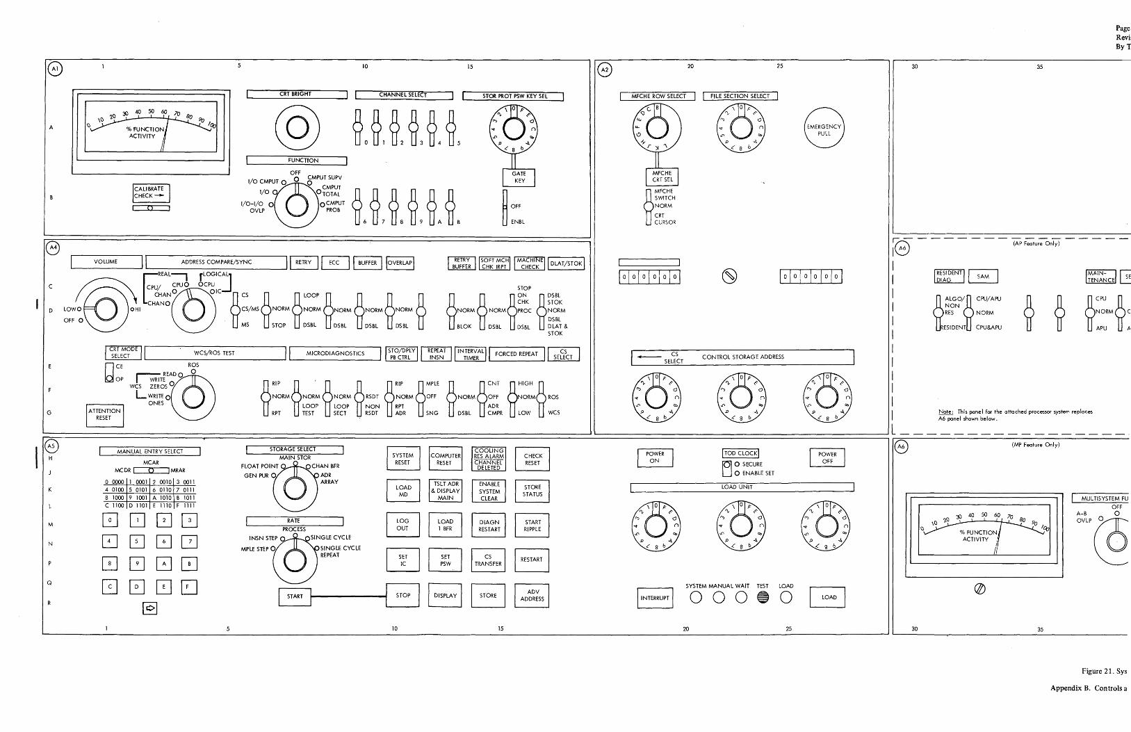
A
C
D
G
10
CRT BRIGHT CHANNEl SElECT
FUNCTION
L--__ V_O_LU_M_E __ ~II L -,-___ A_D_D_RE_S_S_C_O_M_P_AR_E_/S_Y_N_C ___ ----JI ~ ~ [BUffiRJ IOVERLAPI
GREAL• rLOGICAJ
@ CP~AN@CPUO OCP~IC ~CS ~ ~lOOP ~ ~ ~ ~ ~;o OHI CHANO CS/MS NORM NORM NORM NORM NORM
o MS STOP DSBL DSBL DSBl DSBL
J......;;~_~~;;.;;~-"C O.;...T D_E ....... L.. ______ W_C_S_11_RO_S _T_ES_T _____ ........ , L' __ M_IC_R_O_D_IA_G_N_O_S T_IC_5_---' n CE ROS
15
STOR PROT PSW KEY SEl
~ OFF
~ ENBl
L--=-=':'-J
STOP
I DLAT/STOK I
)t~)tORMA~~ UBLOK tr DSBl 'IT DSBL ~
DSBl
STOK NORM
DSBL OlAT & STOK
FORCED REPEAT II SEf~CT
IQ/op ~T~E~@DO 0 WCS ZEROS
LWRlTEo r------, ONES ~RIP ~ "~ ~ ~RIP ~MPlE ~ ~CNT ~HIGH ~ NORM NORM NORM RSDT NORM OFF NORM OFF NORM ROS
LOOP LOOP NON RPT ADR RPT TEST SECT RSDT ADR SNG DSBL CMPR lOW WCS
~MFCHE
SWITCH NORM
CRT CURSOR
_ CS
SELECT
20 25
CONTROL STORAGE ADDRESS
30 35
~ - - - - - - - (APFeatu;;Qn!y) - - --
I I I I I I I I I I I I
SAM
~ALGO/~ CPU/APU NON RES NORM
RESIDENT CPU&APU
Note: This panel for the attached processor system replaces A6 panel shown below.
Page I
Revis ByTl
~==================:::::;:::===================================================::::::=..:============================================; L _________________ . 0) e (MP Feature Only)
H MANUAL ENTRY SELECT
MCAR MC DR .... 1 _ .... 0"-----" MRAR
K o 0000 I 0001 2 0010 3 0011
4 0100 5 0101 6 0110 7 0111
8 1000 9 1001 A 1010 B 1011 C 1100 D 1101 E 1110 F 1111
M 0800 N 80~0
~~00 Q 000~
§]
STORAGE SELECT
CE:J ITOD CLOCKI ~ MAIN STOR ON OFF flOAT POI@AN '" E:J 0 SECURE
GEN PUR 0 ADR o ENABLE SET
ARRAY LOAD UNIT ~ MD
MULTISYSTEM FU
OFF '30 40 50 60 A-B 0
OVLP@ RATE @] G PROCESS OUT 1 BFR
INSN m@GLE CYCLE MPlE STEP 0 SINGLE CYCLE
I RESTART I REPEAT [IJ [JD IC PSW
I DISP~Y I B SYSTEM MANUAL WAIT TEST LOAD
~ START STOP 0 0 0 e 0
5 10 15 20 25 30 35
Figure 21. Sys
Appendix B. Controls a
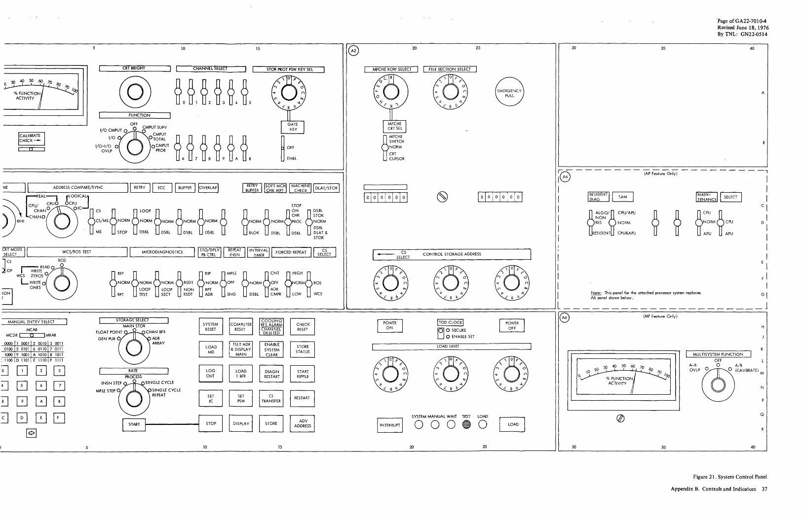
5 10 15
CRT BRIGHT CHANNEL SELECT STOR PROT PSW KEY SEL
@ ~O~'~2~3~'~5 FUNCTION
OFF
I/o CMPU@U:~~~~
~6~7~8~9~A~' I/o a o TOTAL
I/o-I/o ° 0 CMPUT ~ Off OVLP PROB
ENBL
e 20
MFCHE ROW SELECT
~ MfCHE SWITCH NORM
CRT CURSOR
25 30 35
FILE SECTION SELECT
Page ofGA22-7010-4 Revised June 18, 1976 By TNL: GN22-0514
40
A
~ _"'_E __ ...JI ... I-,-___ A_D_D_RE_S_S_C_O_M_P_AR_E_I_SY_N_C ___ -----'I~ EJ I BUFFER IIOVERLAPI
------- ----------- -, (AP Feature Only)
6REAL-, rLOGICAJ
~ CP%AN@CPUO OCP~IC ~CS ~ ~LOOP 0 ~ 0 0 ) OHI CHANO CSIMS NORM NORM NORM NORM NORM
MS STOP DSBL DSBL DSBL DSBL
-....:..:""-'-'~ ~.!:.!....:':':':""::....J ... -==:.:-.....1 I DLAT/STOK I STOP
~ 0 ~ON
CHK
NORM NORM PROC
BLOK DSBL DSBL ~DSBL
STOK NORM
DSBL DLAT & STOK
I I I I I I
CRT MODE II II cS I SELECT L..... _____ W_C_S_/R_O_S_TE_S_T _____ ---I '-__ M_IC_R_O_D_IA_G_N_O_ST_IC_S_----I '--__ .......... __ --' '---'-"-_...... FORCED REPEAT SELECT _ SE~~T CONTROL STORAGE ADDRESS I
SAM SELECT
C
~ ALGO~ cruj Aru
~ ~ ~CPU ~ NON RES NORM NORM CPU D
ESI DENT CPU&APU APU APU
]:: ~T~EA@DO RgS ~ :
WL~:~T~~ ~:~M~NORM NORM ~RSDT ~:~RM~::~E ~NORM~:; ~:I:R:~ROS I ~ ONES LOOP LOOP NON RPT ADR ~ RPT TEST SECT RSDT ADR SNG DSBL CMPR LOW WCS I G I
~~~~~~~~~~==~====================~~==~~~~~~~~~~~~~L~-----------------------~--~J
Note: This panel for the attached processor system replaces A6 panel shown below.
MANUAL ENTRY SELECT
MCAR MC DR ... 1 _ ..... O"'--~I MRAR
0000 1 0001 2 0010 3 0011 0100 5 0101 6 0110 7 0111
1000 9 1001 A 1010 B 1011 : 1100 D 1101 E 1110 F 1111
~80[2J ~0~[J
!J000 ~0~~
~
STORAGE SELECT
MAIN STOR
FLOAT POI@)NQCHANBFR GEN PUR 0 ADR
, ARRAY
RATE
PROCESS
MPLE STEP 0 SINGLE CYCLE REPEAT
INSN ST@ESINGLECYCLE
START
~ ~
STOP I DISPLAY I
10 15
fPOWERl ~
ITOD CLOCKI
ro1 0 SECURE
U 0 ENABLE SET
LOAD UNIT
SYSTEM MANUAL WAIT TEST LOAD
oooeo 20 25
e (MP Feature Only)
H
K MUL TlSYSTEM FUNCTION
OFF L A-B 0 AlB
OVLP (~)CAL"",TE):
Q
30 35 40
Figure 21. System Control Panel
Appendix B. Controls and Indicators 37
If the term you are seeking does not appear in this glossary, refer to Data Processing Glossary, GC20-1699.
Address Translation: The process of changing the address of an item of data or an instruction from its virtual address to its real storage address.
AP: Attached processor.
APU: IBM 3062 Attached Processing Unit Model 1 (described in Appendix G).
Basic Control (BC) Mode: A mode in which the features of a System/360 computing system and additional System/ 370 features, such as new machine instructions, are operational on a System/370 computing system.
CCP: Configuration control panel.
Clock Comparator: A machine timer for measuring elapsed time.
Control Registers: A set of registers used for operating system control of relocation, priority interruption, program event recording, error recovery, and masking operations.
Dedicated: A system resource (I/O device, program, or system) assigned to a single application or purpose.
Dynamic Address Translation (DAT): (1) The change of a virtual storage address to a real storage address during execution of an instruction. (2) A hardware feature that performs the translation.
ECC: Error checking and correction.
EPO: Emergency power off.
Extended Control (EC) Mode: A mode in which all the features of a System/370 computing system, including dynamic address translation, are operational.
Hard Stop: Faulty machine condition in which CPU ceases operation.
ICR: Independent component release.
IDAL: Indirect data address list (used in indirect data addressing feature).
Page ofGA22-70104 Revised June 18, 1976 By TNL: GN22-0S14
Appendix C. Glossary and Abbreviations
Initialize: To set counters, switches, addresses, etc., to 0 or other starting values at the beginning of, or at prescribed points in, a computer program.
Instruction Processor: A computer unit that can independently interpret and execute a sequence of instructions (computer program).
Interval Timer: A machine timer for measuring elapsed time.
[DCA: I/O channel area.
IPL: Initial program load.
ISC: Integrated storage control feature.
K: In storage capacity, 1,024 bytes.
MC: Monitor call (or machine check).
MCEL: Machine check extended logout.
MCU: IBM 3068 Multisystem Communication Unit.
MP: Multiprocessor or the multiprocessor mode.
MSAM: Multisystem activity meter.
OLTEP: Online Test Executive Program.
OS/VS: Operating system/virtual storage.
PER: Program event recording.
Prefixing: In a multiprocessor system, a means for assigning addresses 0 to 4,095 to any 4,096-byte area of processor storage, starting at an address that is a multiple of 4,096.
PSA: Permanent storage area.
PSCF: Processor storage control function.
PVR: Prefix value register.
Appendix C. Glossary and Abbreviations 39
Page of GA22-7010-4 Revised June 18, 1976 By TNL: GN22-0514
Real Address: A location in processor storage.
f SIGP: Signal processor.
Soft Stop: Stop condW.on in which CPU clock continues to run.
STIDP: Store CPU ID.
SVP: Service processor.
TLB: Translation lookaside buffer.
TOD: Time-of-day (clock).
UP: In a multiprocessor system, the uniprocessor mode of operation.
Virtual Address: An address that refers to virtual storage and must therefore be translated into a real storage address when it is used.
40
This optional feature provides for the attachment of up to four 3333 or 3340-A2 drives., Up to three 3330 drives can be attached to each 3333, or up to three 3340 Model B drives can be attached to each 3340-A2. Thus a total of 32 drives can be attached to the ISC (see Figure 22).
This feature, which executes IBM DASD type commands, is organized functionally into two separate data and control paths, each capable of att~ching up to 16 drives. The two paths are logically independent, with completely overlapped operation, and each can attach to separate 2880 Block Multiplexer Channels.
Facilities
The integrated storage control feature provides or supports the following:
• Command Retry
• Multiple Requesting
• Multiple Track Operation
• Record Overflow
• End of File
• Two-channel Switch Optional Feature
• 32-drive Expansion Feature
• 3330/3340 Intermix Feature
Command Retry
Command retry is a channel-storage control procedure that causes an improperly executed command in a channel program to be automatically retried. The re-execution does not cause an I/O interruption, and programmed errorrecovery procedures are not required.
Multiple Requesting
Use of block multiplexer channels and disk drives with rotational position-sensing capabilities allow each ISC path and its attached drives to disconnect from the channel during mechanical delays resulting from execution of arm-positioning seek sector or set sector commands. Reconnection is attempted when the access mechanism is positioned at the desired track or when the specified rotational position has been reached.
During the time the channel and the ISC path are disconnected, the CPU is free to initiate I/O operations on other drives attached to the ISC path even thOUgh the disconnected channel program is not completed. Thus, separate channel programs may be operating simultaneously on each drive attached to the integrated storage control.
Multiple Track (MT) Operation
On all search and most read commands, each ISC path can automatically select the next sequentially numbered head
Appendix D. Integrated Storage Control Feature
on a drive. This eliminates the need for seek head commands in a chain of read or search commands.
Record Overflow
The record overflow function provides a means of processing logical records that exceed the capacity of a track. When using overflow records, the cylinder boundary is the factor limiting the size of the record.
A special channel command (write special count, key, and data) is used to format the disk pack for record overflow operation.
End of File
An end-of-file record, used to define the end of a logical group of records, is written by executing a write count, key, and data command with a data length of zero. Execution of this command causes the ISC to direct the addressed drive to write a data area consisting of one byte of zeros.
When the end-of-file record is processed, detection of the zero data length causes unit exception status to be generated.
Two-channel Switch Feature
This optional feature provides for the attachment of an additional 2880 Block Multiplexer Channel to each data and control path. The channels can be attached to either the same or different CPUs, and individual drives attached to the ISC can be reserved for the exclusive use of any of the four paths. Channel switching and device reservation are con trolled by the channel program. Two special commands are associated with two-channel switch operation: device reserve and device release.
32-drive Expansion Feature
This feature permits the attachment of up to two additional 3333 or 3340-A2 drives to each path of the ISC. With the associated 3330 or 3340 Model B drives, the total available capacity of the ISC is increased to 64 drives, 32 to each path (see Figure 22). A prerequisite for 32-drive expansion is the control store extension feature which provides additional control storage for microprogram use.
Staging Adapter for ISC
This optional feature provides a means for attaching an IBM 3850 Mass Storage System to a Model 168. It offers the same functions as the IBM 3830 Storage Control Model 3. This adapter enables each of the two paths of an ISC to attach as many as four 3333s, each with as many as four 3330s, to a maximum of 32 drives per path. It requires that the ISC have the control store extension feature.
Appendix D. Integrated Storage Control Feature 41

3330/3340 Intermix Feature Statistical Usage/Error Recording
With the prerequisite control store expansion feature installed, this feature permits attachment of up to four 3333 or 3340-A2 drives to each ISC path in any combination. This provides a total of 64 intermixed drives on each ISC.
The ISC maintains a statistical data record of usage and error information for each attached logical device. The usage information provides an accumulated count of the total number of access motions, and the total number of seek errors, correctable data errors, and uncorrectable data
Block Multiplexer Channell
Block Multiplexer Channel 2
Block Multiplexer Channel 3
Block Multiplexer Channel 4
Two-channel Switch Feature
* Optional 32-drive expansion feature.
, .........
./ /
r----------------l I I I I I I I I I I I I I I I I L ________________ J
>-- - --J-L./-74'74'.,.c,e----'----t'/
~----~y~---JA~--------_Tv----------~ 3333 or 3340-A2 Up to three additional 3330 or
3340-81 or -82 drives
I -------------1
I I I I I I I I I I I I I I ~--------------~
Figure 22. Integrated Storage Control Showing Two-channel Switch and 32-drive Expansion
42

errors that were recovered by the ISC retry procedure. Also included in the error information is the total number of command and data overrun conditions that were retried by the ISC.
The usage/error information is sent to the system log area periodically. The transfer takes place on the next start I/O issued to the device having outstanding usage/error information. Each of the usage/error counters is reset to 0 after the counter information is transferred to the channel.
Storage Control Diagnostic Tests
To provide maximum facility availability, each ISC path can execute diagnostic tests on a drive, concurrent with normal system operation on the remaining drives. This mode of operation allows servicing personnel to diagnose and repair most drive failures while the facility continues to operate other attached drives. The ISC provides a transient block of 512 bytes (128 words) of control storage to allow temporary residence for a specific diagnostic test.
The transient area is loaded by the system under control of the Online Test Executive Program (OLTEP). A special command (diagnostic write) loads a selected test into control storage and instructs the storage control to execute the test. This loading and execution may also be initiated from the customer engineering panel.
After the test, error-message information or test results are transferred from the ISC to processor storage by a read diagnostic status 1 command. If the customer engineering panel is used, the test results are displayed on the customer engineering panel indicators.
ISC CONFIGURATION CONTROL
ISC 1
INTERFACE
iON OFF
ISC 2
INTERFACE
~ON OFF
Figure 23. Configuration Control Switches
Configuration Control
Page ofGA22-70104 Revised June 18. 1976 By TNL: GN22-0S14
Operator-accessible switches are provided for configuration control of each ISC data and control path (see Figures 23 and 24). The ISC can operate with a given channel only when the respective interface switch is set to ON. The muItitag switches determine how the device end (generated by the drive in a not-ready-to-ready sequence) is provided to the channel.
Multitag ON Position: A drive is available to a channel after the channel clears the device end generated by the drive on a not-ready-to-ready sequence. Before any other channel can use the drive, it must also accept the not-ready-to-ready sequence device end.
Multitag OFF Position: A drive is available to all channels after one of the channels clears the device end generated by the drive in a not-ready-to-ready sequence.
Interface Time-out Considerations
The control unit may exceed the 32-microsecond initialselection time limit.
I nput/Output Operations
This section contains a general description of I/O operations related to the ISC and its attached disk storage units. For detailed information regarding the central processing unit and channel 'program control of I/O operations, refer to IBM System/370 Principles of Operation, GA22-7000.
ISC CONFIGURATION CONTROL
ISC 1
INTERFACE A INTERFACE B MUlTITAG
~ON OFF
~ON OFF
iON OFF
ISC 2
INTERFACE A INTERFACE B MU lTi TAG
iON OFF
iON OFF
iON OFF
Figure 24. Configuration Control Switches (with Two-channel Switch Feature)
Appendix D. Integrated Storage Control Feature 43
Unit Selection and Device Addressing
The I/O address of each ISC data and control path and its attached drives is designated by an eight-bit binary number in an I/O instruction. These addresses consist of three parts: (1) the ISC data and control path address (determined by servicing personnel at installation time) in bits 0, 1, 2, and 3; (2) the address of the 3333 Disk Storage specified in bit 4; and (3) the addresses of the attached 3330s specified in bits 5,6, and 7.
The ISC accepts any drive address from 000 to Ill. If the specified drive is either not attached or offline, the attempted operation is terminated with unit-check status. Multiple responses to an address because of duplicate logical address plugs or hardware failures also cause the operation to be terminated.
Channel Commands
The command set used to perform operations with the ISC is identical to that used with the 3830 Model 1/3330 Disk Storage facility. For a complete description of these commands, refer to the Reference Manual for Integrated Storage Control, GA26-1620.
Sense Commands Sense I/O Read and Reset Buffered Log Read Diagnostic Status 1 Device Reserve * Device Release *
* Used with two-channel switch optional feature only.
44
Control Commands No-operation Seek Seek Cylinder Seek Head Recalibrate Restore (executed as a no-operation) Set File Mask Space Count Set Sector Diagnostic Write Diagnostic Load
Read Commands Read Data Read Key and Data Read Count, Key, and Data Read Home Address Read Count Read Initial Program Load Read Sector Read Record Zero
Write Commands Write Home Address Write Record Zero Write Count, Key, and Data Write Special Count, Key, and Data Erase Write Data Write Key and Data
Search Commands Search ID Equal Search Key Equal Search Home Address Equal Search ID High Search Key High Search ID Equal or High Search Key Equal or High
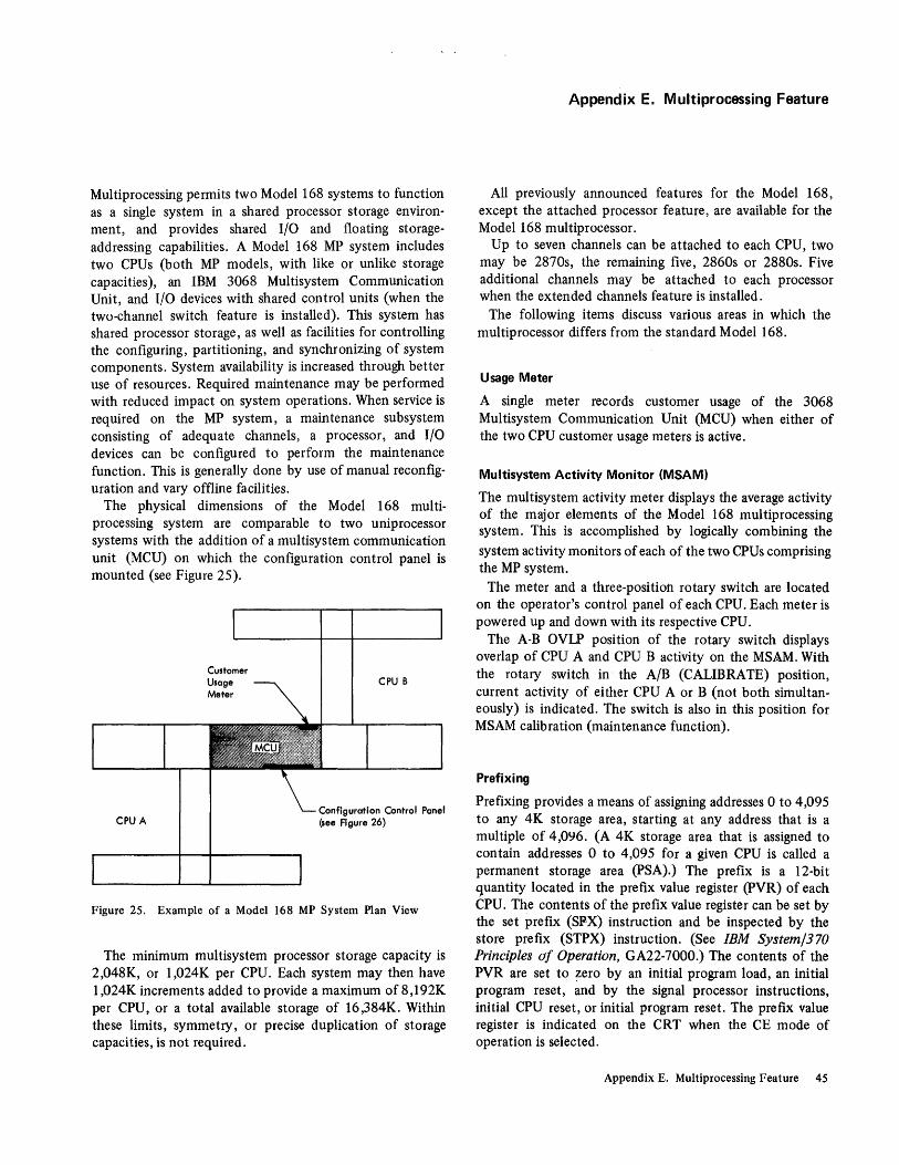
Multiprocessing permits two Model 168 systems to function as a single system in a shared processor storage environment, and provides shared I/O and floating storageaddressing capabilities. A Model 168 MP system includes two CPUs (both MP models, with like or unlike storage capacities), an IBM 3068 Multisystem Communication Unit, and I/O devices with shared control units (when the two-channel switch feature is installed). This system has shared processor storage, as well as facilities for controlling the configuring, partitioning, and synchronizing of system components. System availability is increased through better use of resources. Required maintenance may be performed with reduced impact on system operations. When service is required on the MP system, a maintenance subsystem consisting of adequate channels, a processor, and I/O devices can be configured to perform the maintenance function. This is generally done by use of manual reconfiguration and vary offline facilities.
The physical dimensions of the Model 168 multiprocessing system are comparable to two uniprocessor systems with the addition of a multisystem communication unit (MCU) on which the configuration control panel is mounted (see Figure 25).
CPU A
Customer Usage Meter
CPU B
Configuration Control Panel (see Fi gure 26)
Figure 25. Example of a Model 168 MP System Plan View
The minimum multisystem processor storage capacity is 2,048K, or 1,024K per CPU. Each system may then have 1,024K increments added to provide a maximum of8,192K per CPU, or a total available storage of 16,384K. Within these limits, symmetry, or precise duplication of storage capacities, is not required.
Appendix E. Multiprocessing Feature
All previously announced features for the Model 168, except the attached processor feature, are available for the Mode1168 mUltiprocessor.
Up to seven channels can be attached to each CPU, two may be 2870s, the remaining five, 2860s or 2880s. Five additional channels may be attached to each processor when the extended channels feature is installed.
The following items discuss various areas in which the multiprocessor differs from the standard Model 168.
Usage Meter
A single meter records customer usage of the 3068 Multisystem Communication Unit (MCU) when either of the two CPU customer usage meters is active.
Multisystem Activity Monitor (MSAM)
The mUltisystem activity meter displays the average activity of the major elements of the Model 168 multiprocessing system. This is accomplished by logically combining the
system activity monitors of each of the two CPUs comprising the MP system.
The meter and a three-position rotary switch are located on the operator's control panel of each CPU. Each meter is powered up and down with its respective CPU.
The A-B OVLP position of the rotary switch displays overlap of CPU A and CPU B activity on the MSAM. With the rotary switch in the A/B (CALIBRATE) position, current activity of either CPU A or B (not both simultaneously) is indicated. The switch is also in this position for MSAM calibration (maintenance function).
Prefixing
Prefixing provides a means of assigning addresses ° to 4,095 to any 4K storage area, starting at any address that is a multiple of 4,096. (A 4K storage area that is assigned to contain addresses ° to 4,095 for a given CPU is called a permanent storage area (PSA).) The prefix is a 12-bit quantity located in the prefix value register (PVR) of each CPU. The contents of the prefix value register can be set by the set prefix (SPX) instruction and be inspected by the store prefix (STPX) instruction. (See IBM System/370 Principles of Operation, GA22-7000.) The contents of the PVR are set to zero by an initial program load, an initial program reset, and by the signal processor instructions, initial CPU reset, or initial program reset. The prefix value register is indicated on the CRT when the CE mode of operation is selected.
Appendix E. Multiprocessing Feature 45

Prefixing operates as follows: when a CPU references a storage address in the range of 0 to 4,095 (the high-order twelve bits, 8 to 19, of the effective storage address are zeros), the contents of the prefix value register for that CPU are added to bits 8 to 19 of the effective address. The new address then points to a location within the PSA of the referencing CPU. This is called forward prefixing. Only forward prefixing is used for channel storage requests. When a CPU references an address in the 4K block that is pointed to by its PVR (that is, an address in its own PSA), zeros are substituted for bits: 8 to 19 of the effective address so that an address range of 0 to 4,095 results. This is called reverse prefixing. This essentially provides the capability for the CPU to access the now unused address range of 0 to 4,095. A value of zero in the PVR effectively disables prefixing. Certain channel stoql.ge requests (CCW, extended log, IDA, data) are not prefixed.
CPU Signaling and Response
The signal processor (SIGP) instruction provides a means of communication between two CPUs of an MP system. The facility receives the signal, decodes a set of assigned order codes, performs the specified operation, and responds to the signaling, CPU (CPU A is assigned address 00; CPU B is assigned address 01). Twelve orders are used for interprocessor communications. They are specified in bit positions 24 to 31 of the second operand address of the SIGP instruction and are encoded as follows:
Code
00 01 02 03 04 05 06 07 08 09 OA OB OC
OD-FF
Order
Unassigned Sense External Call Emergency Signal Start (see Note) Stop Restart Initial Program Reset Program Reset Stop and Store Status Initial Microprogram Load Initial CPU Reset CPU Reset Unassigned
Note: When a Model 168 MP CPU is in the stopped state with an I/O interruption pending and the SIGP start order code (04) is received, the interruption is taken prior to, instead of after, the execution of the first instruction.
Details concerning the signal processor instruction, and additional new instructions, specifically, store CPU address (ST AP), set prefix (SPX), store prefix (STPX), compare and swap (CS), compare double and swap (CDS), insert PSW key (IPK), set PSW key from address (SPKA), and clear I/O (CLRIO), can be found in IBM System/370 Principles of Operation, GA22-7000.
46
Shared Storage
Communication between CPUs becomes active when both CPUs read a valid shared-storage configuration from the configuration control panel. This ensures that all references to shared storage access the most current data.
Storage Control
When MP is installed, storage-use priority is established every cycle. First, priority is established within a CPU; and then priority is established between CPU s. Dependent upon priorities, neither CPU is permitted two successive refer::nces to a particular logical storage unit if the other CPU has a request pending for that unit. ~o ensure proper sequence of data manipulation between
CPUs, data stored by one CPU and fetched by the other appears to the fetching CPU to have been stored in the order designated by the instruction sequence.
Storage Protect
The storage protection hardware is located in each storage complex and protects up to eight megabytes of storage in each CPU of a multiproceSSing system. Blocks of data which are 2K in size can be protected against store or fetch violations.
Malfunction Alert
In MP mode when the remote CPU enters the check-stop state or loses power, a malfunction alert is generated. The address of the issuing processor is stored in locations 132-133 with an interruption code of 1200 (hex). The condition remains pending until the system is reset.
Time-of-day (TOO) Clock
The Model 168 MP system uses the TOD clock provided in each CPU to do the system clocking. Clock synchronization is a programming-dependent function and is assisted by hardware. Once synchronized, the two clocks appear as one clock to the system. See "TOD Clock Synchronization" in IBM System/370 Principles of Operation, GA22-7000.
Power Control
The power-on switch on a CPU brings power up on that CPU and both the shared and nonshared units controlled by that CPU. The power-off switch removes power from that CPU and the nonshared units controlled by that CPU. Neither switch is effective on a CPU that has its remote/ local switch set to LOCAL. EPO removes power from all units.
The following configuration criteria must be entered into the system before powering-down the units: 1. To power-down a CPU, with or without its channels, no •
storage should be enabled to the powered-down CPU. The system must be in UP mode.
2. * To power-down a storage gate, the oscillator control switch must be set to the other system and no CPU may be enabled for the powered-down storage gate.
3.* To power-down half of the multisystem communication unit (MCU): a. No storage physically attached to one CPU may be
enabled to the other CPU (not cross-configured). b. The CPU associated with the half of the MCU to be
powered-down may not be in operation. c. The oscillator control switch must be set to the
remaining system which must be operating in UP mode.
4. To power-down a channel, the channel power control switch must be set to LOCAL, the interface disable switch must be on, and the CPU must have passed through the wait or stopped state.
5. * The integrated storage control must be varied offline by the operating system.
To power-up a unit (bring it into the system), the same criteria must be met, even though hardware interlocks ensure that a nonfunctional configuration cannot 'be entered. * Maintenance function.
MCU Power Control
The multisystem communication unit consists of two logical gates: A and B. The power and cooling for each gate is supplied by its respective CPU. Each gate has a separate power control panel mounted on the MCU. This panel contains the power control selector switch which determines the power sequencing of each gate. The use of either local or system power control provides flexibility in maintenance of the system.
Resets
Several different types of reset exist on the Model 168 multiprocessor: power-on, program, initial program, system clear ,. and CPU. Resets having programming significance are discussed below. Program Reset: This reset can be initiated by any of the following: 1. Pressing SYSTEM RESET. This also causes a program
reset in the other CPU if it is configured.
Note: If either of the enable system clear pushbuttons is held in, proces.sor storage, general registers, and floating-point registers are cleared in both CPUs.
2. Pressing LOAD. This also causes a program reset in the other CPU if the system is in MP mode.
3. Issuing SIGP with the program reset function code (08) to the addressed CPU. The following actions are taken: a. The current CPU operation is terminated. b. All pending program or SVC interruptions are
cleared. c. All pending I/O and external interruptions are
cleared. d. All pending machine-check conditions and error
indications are cleared. e. Reset signals are issued to all configured channels and
I/O control units. f. The CPU is placed in the stopped state. Processing
can be initiated without being affected by any previously detected unusual events.
The contents of the programmable registers are left unaltered-unless either of the enable system clear pushbuttons is held in. Initial Program Reset: This reset can be initiated by any of the following: 1. Pressing LOAD with the enable system clear pushbutton
held in. 2. Issuing SIGP with the initial program reset function
code (07) to the addressed CPU. Initial program reset results in the same actions as taken in Step 3 in ~'Program Reset." In addition: a. The contents of the control registers are initialized. b. The contents of the PSW, prefix value register, CPU
timer, and clock comparator are cleared. The general and floating-point registers remain unaltered.
System Clear: This reset can be initiated in MP mode by any of the following: 1. Pressing SYSTEM RESET on either CPU, with either
enable system clear pushbutton held in. 2. Pressing LOAD on either CPU, with either enable system
. clear pushbutton held in. System clear causes the same actions to be taken as in
"lllitial Program Reset." In addition: 1. The general and floating-point registers are set to zero
with valid parity. 2. The contents of processor storage and the keys in
storage are set to zero with valid parity depending on configuration.
Initial CPU Reset: This reset can only be initiated by the SIGP order code (OB). It performs the functions of initial program reset except that: 1. Channels are not reset. 2. Pending I/O interruptions are not cleared in the channel.
CPU Reset: This reset is initiated either by pressing COMPUTER RESET on the console or by issuing the SIGP
. CPU reset order code (OC). It performs the functions of program reset except that: 1. Channels are not reset. 2. Pending I/O interruptions are not cleared in the channel.
Appendix E. Multiprocessing Feature 47
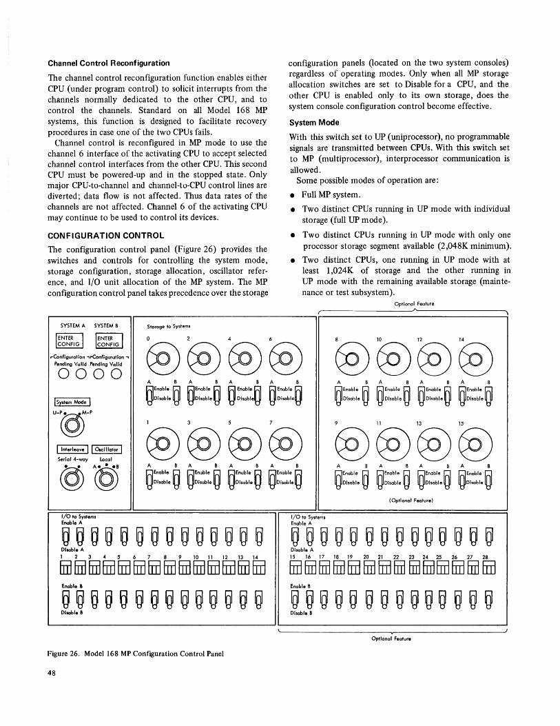
Channel Control Reconfiguration
The channel control reconfiguration function enables either CPU (under program control) to solicit interrupts from the channels normally dedicated to the other CPU, and to control the channels. Standard on all Model 168 MP systems, this function is designed to facilitate recovery procedures in case one of the two CPUs fails.
Channel control is reconfigured in MP mode to use the channel 6 interface of the activating CPU to accept selected channel control interfaces from the other CPU. This second CPU must be powered-up and in the stopped state. Only major CPU-to-channel and channel-to-CPU control lines are diverted; data flow is not affected. Thus data rates of the channels are not affected. Channel 6 of the activating CPU may continue to be used to control its devices.
CONFIGURATION CONTROL
The configuration control panel (Figure 26) provides the switches and controls for controlling the system mode, storage configuration, storage allocation, oscillator reference, and I/O unit allocation of the MP system. The MP configuration control panel takes precedence over the storage
SYSTEM A SYSTEM 8
I ENTER I I ENTER I ICONFIGJ ICONFIG
.. Configuration .,..eanfigurotion ., Pending Valid Pending Valid
0000
I System Mode I
Storage to Systems
1 3 5 7
configuration panels (located on the two system consoles) regardless of operating modes. Only when all MP storage allocation switches are set to Disable for a CPU, and the other CPU is enabled only to its own storage, does the system console configuration control become effective.
System Mode
With this switch set to UP (uniprocessor), no programmable signals are transmitted between CPUs. With this switch set to MP (multiprocessor), interprocessor communication is allowed.
Some possible modes of operation are:
• Full MP system.
• Two distinct CPUs running in UP mode with individual storage (full UP mode).
• Two distinct CPUs running in UP mode with only one processor storage segment available (2,048K minimum).
• Two distinct CPUs, one running in UP mode with at least I,024K of storage and the other running in UP mode with the remaining available storage (maintenance or test subsystem).
Optional Feature ~ ________________ ~A ________________ ~,
9 11 13 15
I Interleave II Oscillator I
@'@ @@@@ @@@@
A B A B A B A B
REnable R REnable R ~Enable R InIEnable ~
\jIDisable ij 'tjDisable 'tj '\:lDisable ~ \:l'Disable Il:J
I/O to Systems Enable A
ijijijij~~ijijijijijijijij Disable A
1 2 3 4 5 6 7 8 9 10 11 12 13 14
fill fill fill fill fill fill fill fill fill fill illHra fill fill
Enable B
ijijijijij~ijijijijij~ijij Disable B
I/O to Systems Enable A
(Optional Feature)
ij~ijij~~~ijijijijijijij Disable A 15 16 17 18 19 20 21 22 23 24 25 26 27 28
fillrnJfillfillfillfillfillfillrnJfillfillfillfillfill
Enable B
ijij~ijij~ijijij~ijijijij Disable B
. Optional Feature
Figure 26. Model 168 MP Configuration Control Panel
48

• One CPU running in UP mode with.all available storage.
• MP system running with one processor storage segment available (l.024K minimum).
Storage to Systems Allocation
Enable/Disable: Enable/disable switches, one per CPU, are associated with each rotary floating address switch. Each switch, in conjunction with the ENTER CON FIG pushbutton, enables or disables the operation of the associated CPU with a segment of storage. The blocks of addresses assigned to a CPU need not be contiguous. However, address range 0-1,024K must always be assigned. Failure to do this prevents completion of initial program load (IPL).
Storage Addressing: Up to 16 rotary floating address switches are available. Each switch assigns an address range to one segment of storage, which gives the system a maximum floating address capability of 16,384K. Assignments selected by these switches become effective when the ENTER CONFIG pushbutton is pressed and the configuration pending indicator is turned off. Floating storage addressing is functional for both serial and four-way interleaved modes of operation.
ENTER CONFIG Pushbutton
An ENTER CONFIG pushbutton for each CPU is provided. Pressing this pushbutton results in the enter configuration signal as soon as the affected CPU passes through either the wait or stopped state. The position of storage allocation, floating address, system mode, and oscillator control switches is determined. If the settings are valid, the information is entered into configuration control registers. If the configuration entered contains cross configuration,
or if the oscillator control switch is changed, the enter configuration request generated by either pushbutton is registered in both CPUs. Such a request is only effective at the time both CPUs pass through the wait or stopped state simultaneously.
While the enter request is pending, the configuration pending light is on. If any configuration switches are changed during this time, the result is unpredictable.
If the configuration is invalid, the valid configuration indicator stays off until a valid configuration is placed in the switches. The configuration pending light also stays off. After correcting the individual switch settings, ENTER CONFIG must be pressed to initiate a new enter request.
Interleave
This two-position rotary switch controls the selection of either serial or four-way interleaved mode of operation. Four-way interleave is the normal mode of operation.
Oscillator Control
This three-position switch controls the timing oscillators as follows:
A position: Both CPUs operate from the time-of-day and system oscillators associated with CPU A.
B position.~ Both CPUs operate from the time-of-day and system oscillators associated with CPU B.
Local position: Each CPU operates with its local oscillators. This position is valid only in UP mode. The switch may be left in either the A or B position for most configurations.
Configuration Pending/Valid Indicators
If a valid configuration indicator is not lit when the associated ENTER CON FIG pushbutton is pressed, the configuration remains unchanged. The pending indicator is lit from the time that the ENTER CONFIG pushbutton is pressed (if the configuration is valid) until the enter configuration signal is issued.
The valid configuration indicator not being lit could be caused by one or more of the following conditions:
Double Addressing: Two or more floating address switches are set to the same range and have their allocation switches enabled for the same CPU.
. Partial Sharing: Some assignable segment of processor storage is assigned to both CPUs and some other segment is assigned to only one CPU.
Split Oscillator: The system mode switch is set to MP, but the oscillator control switch is set to Local.
Cross-configured Split Oscillator: A storage attached to CPU A is enabled to CPU B, or a storage attached to CPU B i.s enabled to CPU A (cross-configured), with the oscillator control switch set to Local.
Unpowered Oscillator: If the oscillator control switch is set to an oscillator that is powered down, an invalid configuration is detected.
Cross-configured MP MCU Powered Down: If storage attached to CPU A is enabled to CPU B while the MP gate for CPU A is powered down, CPU B detects a configuration error. The reverse situation also holds true.
Appendix E. Multiprocessing Feature 49
Shared Storage in UP Mode: Any storage being shared with the system mode switch in the UP mode position.
Loosely Coupled: If the system is in MP mode and all enabled storage is not shared, a configuration error is indicated.
Partial MP System: If the system is in MP mode and either CPU is powered down, a configuration error is detected.
Unavailable Storage: A segment of storage (I,024K) is enabled but not powered up or installed.
Allocation Switches (I/O to Systems)
These 14 or 28 pairs of switches (14 standard, 14 optional) provide for the attachment of control units having the remote switch attachment installed. They are independent of the enter configuration pushbutton. The square space between the rows of switches holds identification nomenclature for the control units.
50
The power warning feature on the Model 168, supported by an uninterruptible power system, permits controlled shutdown and recovery procedures following power line disturbances. A power drop of 18 ± 2% below rated input voltage causes the uninterruptible power system to activate a system warning signal. The power warning feature responds by providing an automatic interruption to the control program. Combined with OS/VS or OS/MVT programming, power warning provides support for:
• Turning on the power warning bit.
• Timed delay prior to the user exit and dump routine.
• User intercept option.
• Processor storage dump restore.
The uninterruptible power system can, during power line disturbances (including complete loss of power), supply emergency power to either the complete computing system or to critical components of the system. With uninterruptible power supplied to the complete system, operation may continue during power failures as long as the interruption does not exceed the capacity of the emergency power source.
A partial uninterruptible power system provides power to the CPU, all channels, and those control units and devices required on the dump channel.
The user intercept option permits the user to program (via an exit) ride-through and quiesce procedures that are tailored to his particular operation.
The elements of the field-installable power warning feature are:
• A vendor-supplied uninterruptible power system that detects power line disturbances, provides a power warning signal, and maintains power to either the full system or to critical components of the system.
• Minor hardware modifications to the Model 168.
• Software support for the power warning machine-check interruption handler, the dump and restore programs, and the user intercept option.
Operational Characteristics: The warning is issued when the input power voltage drops 18 ± 2% and remains down longer than one-half cycle. The uninterruptible power system sensor signal remains active as long as the undervoltage condition exists, and causes the CPU to generate a soft machine-check interruption. This interruption is under the control of PSW bit 13 (machine-check interruption mask), and bit 7 of control register 14 (power warning submask).
If the user provides an uninterruptible power system for his entire system, the following events occur:
Appendix F. Power Warning Feature
• The interruption branches to a timing routine to determine if the power disturbance is transient. The duration of this timing activity is a customer option and is limited by uninterruptible power system reserve power.
• If the disturbance is transient, control returns to the machine-check handler and the system continues operation.
• If the disturbance is nontransient, control passes to the user intercept option and then to the dump routine.
The user intercept option allows the user to: 1. Ride through a short duration power line disturbance
that exceeds the timed delay. 2. Assess the reserve time left in the uninterruptible power
system to justify continued processing. 3. Initiate his system quiesce procedures to terminate
operations within the limits of his uninterruptible power system reserves. These procedures must be developed by the user.
4. Transfer to the dump routine which terminates all processing and preserves the contents of storage for subsequent restart procedures.
If the dump routine is selected, system storage can be reloaded from the dump device when normal power is restored. This storage information is then available to assist the user in recovery and restart procedures.
Multiprocessing: In a tightly coupled multiprocessing system, the power warning signal is sent to both CPUs. Masking in the individual CPUs determines if the interruption is processed or held pending. In MP mode, all shared storage can be dumped by either CPU depending on which one processes the interruption. To dump all storage, power must be on and auxiliary power supplied to both halves of the MP system including the 3068 Multisystem Communication Unit (MCU). In uniprocessor mode, each CPU must process its own interruption. Only that storage configured to a CPU can be dumped by that CPU. If both CPUs require the power warning feature in the uniprocessor configuration, they must both have a control unit connected to the uninterruptible power system.
Physical Planning: (Ref: A Guide to 60 Hz Uninterruptible Power System Selection, GA27-2770) Installation of either a partial or full uninterruptible power system requires a significant amount of preinstallation planning. Specialists are required to determine the uninterruptible power system specifications, space requirements, cable layout, etc. Users should allow six months to a year lead time prior to the desired installation date.
Appendix F. Power Warning Feature 51
Page of GA22-70104 Revised June 18, 1976 By TNL: GN22-0S14
Appendix G. Attached Processor Feature
An IBM 3062 Attached Processing Unit (APU) Modell is added to an IBM 3168-3 Processing Unit to create the attached processor function. The CPU and APU act as a single, tightly coupled system with shared processor storage. The Model 168 attached processor system also requires the following units: an IBM 3066 System Console Model 3 and an IBM 3067 Power and Coolant Distribution Unit (Model 3 for the 3168-3 and Model 5 for the 3062 APU). The field-installable upgrade to the Model 168 entails a model change on the console, and a feature addition to the power distribution unit and CPU.
All previously announced optional features for the Model 168 except for multiprocessing are available for the CPU of an attached processor system. Processor storage incremen ts for the CPU are 1 ,024K, with a minimum of 1,024K and a maximum of 8,192K. Up to seven channels can be attached to the CPU; five additional channels may be added when the extended channels feature is installed.
The APU is an instruction processor that implements the same System/370 facilities as described in this manual for its host Model 168 CPU. The five exceptions are: direct control, I/O, processor storage, emulator, and console. 1. The APU does not support the direct control facility;
direct control is supported only by the CPU. 2. I/O is nonnally handled only by the CPU. Because the
APU has no channels attached, execution of I/O instructions nonna1ly returns a condition code of 3, indicating that the channel is not operational.
3. The APU shares processor storage with the host CPU. The storage controls of the APU communicate with those of the CPU to enable all of processor storage to be used by both instruction processors.
4. The APU does not support emulation. 5. The APU has no separate console.
With consideration to the preceding items, this manual applies to the instruction processor in both the CPU and APU of an attached processor system. Those items in which the attached processor system differs from a basic Model 168 system are discussed in the following sections.
Usage Meter
The usage meter on the 3066 Model 3 records customer usage when the instruction processor in either the CPU or APU is in operation.
System Activity Meter (SAM)
Under control of the Model 3 extension to the 3066 System Console, the system activity meter can display the average activity of either the CPU or APU or both.
52
With the SAM switch on panel A6 in the NORM position, either CPU or APU activity is displayed, depending on the position of the SELECT switch. With the SAM switch in the CPU&APU position, the overlap (logical AND) of CPU and APU activity is read. In the CPU/APU position, the activity of the CPU or APU (logical OR) is indicated. The system parameter displayed is selected by the function rotary switch on the console.
Note that selection of channel functions is not appropriate for the APU; the APU has no channels attached and has no channel activity.
Prefixing
Prefixing is standard in an attached processor system. Both the CPU and APU have prefix value registers to enable them to assign the pennanent storage area (PSA) of its instruction processor to any 4K storage area, starting with any address that is a mUltiple of 4,096. The 12-bit prefix value in an instruction processor can be set by execution on that instruction processor of the set prefix (SPX) instruction and can be inspected by the store prefix (STPX) instruction. The contents of the prefix value register are set to 0 by an initial program load, an initial program reset, and by the signal processor instructions: initial CPU reset or initial program reset. The prefix value register is indicated on the CRT when the CE mode of operation is selected. Application of prefixing is described in IBM System/370 Principles of Operation, GA22-7000.
CPU Signaling and Response
The signal processor (SIGP) instruction provides communication between the CPU (addressed as processor 01) and the APU (addressed as processor 00) in an. attached processor system. Twelve orders are implemented for interprocessor communication. They are specified in bit positions 24 to 31 of the second operand address of the SIGP instruction and are encoded as follows:
Code Order
00 Unassigned 01 Sense 02 External Call 03 Emergency Signal 04 Start (see Note) 05 Stop 06 Restart 07 Initial Program Reset 08 Program Reset 09 Stop and Store Status OA Invalid (not implemented) OB Initial CPU Reset OC CPU Reset
OD-FF Unassigned

Details concerning the SIGP instruction can be found in IBM System/370 Principles of Operation, GA22-7000.
Processor Addresses
In an attached processor system, the STAP instruction returns an ID of 00 when executed by the instruction processor in the APU and returns an ID of 01 when executed by the instruction processor in the CPU.
Storage Control
Use of processor storage is shared between the CPU and the APU during every other cycle. Dependent upon priorities, the APU is not permitted to make two successive references to the same logical storage unit if the CPU has a channel request pending for that unit.
To ensure prope.r sequence of data manipulation between the CPU and the APU, data stored by one instruction processor and fetched by the other appears to the fetching instruction processor to have been stored in the order designated by the instruction sequence.
Malfunction Alert
Page of GA22-7010-4 Revised June 18. 1976 By TNL: GN22-0S14
When one instruction processor enters the check-stop state, a malfunction alert is generated at the other instruction processor. The address of the failing instruction processor is stored in locations 132-133 of the receiving instruction processor with an interruption code of 1200 (hex). The condition remains pending until the interruption is taken or the system is reset.
Time-of-day (TOO) Clock
The attached processor system uses the TOD clock provided in each instruction processor to do the system clocking. The APU uses the TOD clock oscillator provided by the CPU. Clock synchronization is a programmingdependent function and is assisted by the system. Once synchronized, both CPU and APU clocks appear as one clock to the system.
Power Control
Power must be on to both the CPU and APU for the system to operate. EPO removes power from both the CPU and APU.
Appendix G. Attached Processor Feature 53
Page of GA22·70104 Added June 18, 1976 By TNL: GN22·0S14
Appendix H. Deviations from the IBM System/370 Model 168 Functional Characteristics
Store CPU 10 (STIDP) Instruction
The STIDP instruction when executed on the APU returns the four digits 3062 as the model number in bit positions 3247.
The version codes returned in bit positions 0·7 are:
Hex Code
00 01 81
Version
3168·1 UP or MP 31'68-3 UP or MP 3168-3 AP or 3062-1
The machine-check extended logout (MCEL) length returned in bit positions 46-63 is 1 ,416 decimal bytes (0588 hex).
The CPU identification number in bit positions 8-31 contains the six-digit serial number of the instruction processor. This hexadecimal number corresponds with the physical serial number stamped on frame 03 of the CPU or APU, depending on which unit executes the instruction. The five low-order digits are identical to the five contiguous digits in the physical serial number. The sixth digit is O.
I nterruptions When the Processor Leaves the Stopped State
If an I/O or external interruption is pending when the 3168-3 CPU or 3062 APU leaves the stopped state, the interruption may be taken before rather than after the execution of the first instruction. This applies to leaving the stopped state either by pressing the start pushbutton or because a signal processor (SlOP) start order code was received.
54
Data Exception during Execution of a Divide Decimal Instruction
If a divide decimal instruction (operation code FD) operates on data that contains invalid digits in those portions of the first and second operands that are tested for a divide exception, the processor may indicate a dividedecimal exception (code OOOB) rather than a data exception (code 0007). For invalid signs, a data exception is indicated.
Check-stop Control
If an exigent machine check occurs while PSW bit 13 is 0 and CRI4 bit 0 is 0, and then CRI4 bit 0 is turned on, the processor immediately enters a check-stop state rather than keep the check condition pending.
Serialization for a Write Direct Instruction
The serialization performed for a write direct instruction occurs after rather than before the operand is fetched. Therefore, the first operand may be fetched before previous store operations have been completed as observed by the channels or another instruction processor. However, the first operand of write direct that is fetched contains the correct updated information resulting from any previous store operations by this CPU. All previous store operations by this CPU are completed before the signals are presented.
Enable System Clear Pushbutton
The enable system clear pushbutton is ORed whenever the system mode switch on the configuration control panel is to the M-P position.

abbreviations 39 activity meter, system 21 activity monitor, multisystem 45 addressing the operator's console 27 addressing, storage (MP) 49 algorithm, identification number 54 allocation
storage 48 switches 49
asynchronous checks (OC) 29 attachable I/O devices 5 attached processing unit 6,52 attached processor feature 52
bibliography 31 block multiplexer channel (2880) 20 buffer storage (controls) 12 byte multiplexer channel (2870) 19 byte-oriented operand 9
channels attachment 17 data rate considerations description 17 dual bus 20 extended, feature 20 highligh ts 10
17
to channel adapter 18 central processing unit (CPU) 11 check-stop control 54 check-stop state 25 clear pushbutton, enable system 54 clock comparator 9 commands 27 compatibility between models 5 configuration
control 26, 48 pending/valid 49 storage 16 system 6
console file 26 control(s)
and indicators 32 configuration 48 extended 12 high-speed buffer 12 integrated storage 41 I/O channel 15 MCU power 47 power 46 processor 16 registers 24
CPU (central processing unit) 11 CPU signaling and response 46 CPU timer 9 CRT display 26
data exception, divide decimal 54 description of system 6 deviations 54 direct control 8
display CRT 25 store and 26
document viewer 26 double addressing 49 drive expansion feature 41 dynamic address translation (DAT)
description 12 highlights 10
emergency power off (EPO) 6 enable/disable switches 48 enable system clear pushbutton 54 ENTER CONFIG pushbutton 49 erase command (OC) 28 error interruptions (OC) 30 execution unit 11 extended channels feature 20 extended control 12
features, optional 6 fields, control register 24 functions 22
general system data 10 glossary and abbreviations 39
hardware retry 22 high-speed buffer 12 high-speed multiply 6
identification number 54 identification number algorithm 54 indicate check-stop state 25 indicator viewer 26 indicators
operator's console (OC) 28 pending/valid 48 unique with this model 25
indirect data addressing 18 instruction processor 6, 9 instruction unit 11 integrated storage control 41 interface disconnect 28 interface time-out considerations 43 interleave switch 49 interleaving 16 intermix feature 42 interprocessor communication 45 interruption
after SIGP start order 54 error 30 handling of an 54 machine-check 25 normal 29 OC 29
interval timer 9 introduction 5
Page of GA22-70104 Revised June 18, 1976 By TNL: GN22-0514
Index
Index 55
Page of GA2~-70104 Revised June 18, 1976 By TNL: GN22-0514
I/O attachable devices 5 I/O channel controls (I/O buffer) 15 I/O to systems allocation switches 49
local storage 11 lock keyboard 28 logout (model-dependent) 22
machine check 22, 24 machine-check in terruption 25 main control panel 26 malfunction alert 46 metering, usage 21 mode switch, system 48 model-dependent functions 22 multiprocessing 6, 45 multiprocessor 7 multisystem
activity monitor (MSAM) 45 communications unit 45
no op 28
operating system 5 operations (for programmer) operator's console (OC) 27 optional features 6 oscillator switch 49
partial MP system 49 partial sharing 49 permanent storage area (PSA) permanent storage assignment power control 46 power warning 51 prefix value register 45 prefixing 45 processor
instruction 5, 9 service (SVP) 16
processor storage by model 11 configuration 12
27
45 12,24
con trol function (PSCF) 11 controls 16 interleaving 12 permanent storage area (PSA) 45 permanent storage assignment 12 shared 46
program even t recording 9 programming 5, 27 programming compatibility 5 PSCF 11,13
read 28 read MI 28 read-.only storage (ROS) 11 register, prefix value 45 reset (OC) 28 resets (MP model) 47 retry 22
selective reset 28 selector channel (2860) sense byte 29 serialization, write direct service processor (SVP)
56
18
54 16
set (commands) audible alarm 28 buffer address 27 cursor 27 shared storage 46
software retry 22 split oscillator 49
cross configured 49 standard facilities 8 status byte 29 status indicator 28 storage
addressing 48 allocation 48 assignment, permanent 15, 24 check 25 configuration control 26,48 control diagnostic tests 43 control, integrated 41 data 10 processor 11 protect 46 read -only 16 shared 46 to systems controls 48 unavailable 49 use priority 45
store and display 25 store CPU ID (STIDP) 54 switches (see controls) synchronous checks 29 system
activity meter 21 configuration 6,26 console 26 data, general 10 description 6 highlights 10 loosely coupled 49 mode switch 48 reset (OC) 28 timing facilities 9
System/370 instruction enhancements 8 universal instruction set 8
test I/O 27 time-of-day clock 9, 46 time-out considerations, interface 43 timer, interval 9 TLB operation 14 translation lookaside buffer (TLB) 14 translator 13 two-channel switch 41
unavailable storage 49 uninterruptible power system 51 uniprocessor 7 unpowered oscillator 49 usage metering 21
multisystem 45
valid/pending indicators 49 viewer
document 26 indicator 26

writable control storage 16 write 27 write direct serialization 54
2860 Selector Channel 18 2870 Byte Multiplexer Channel 17, 19 2880 Block Multiplexer Channel 17, 2d 3066 System Console 6 3067 Power and Coolant Distribution Unit 6 316e Processing Unit 6, 11 709/7090/7094/7094 II compatibility 6 7070/7074 compatibility 6 7080 compatibility 6
Page ofGA22-7010-4 Added June 18, 1976 By TNL: GN22-0514
Index 57

Technical Newsletter This Newsletter No. GN22-0514
Date June 18, 1976
Base Publication No. GA22-70104
File No. S/370-01
Previous Newsletters None
IBM System/370 Model 168 Functional Characteristics
©IBM Corp. 1972,1973,1976
This Technical Newsletter provides replacement pages for the subject publication. The foldout is placed at the back of the TNL to facilitate printing and handling. Merge the foldout page with the remainder of the TNL before replacing pages. Pages to be inserted and/or removed are:
Front Cover, Preface Contents, Frontispiece 5-8 15, 16 31-34 35, blank 37, blank 39,40 43,44 51-56 (Page 54 added) 57 (added), Back Cover
All pages to which a change has been made carry a revision notice in the upper margin. A change to the text or an illustration is indicated by a vertical1ine to the left of the change.
Summary of Amendments
This Technical Newsletter corrects information in "Appendix B. Controls and Indicators" and adds "Appendix H. Deviations from the IBM System/370 Model 168 Functional Characteristics."
Note: Please file this cover letter at the back of the manual to provide a record of changes.
IBM Corporation, Product Publications, P.O. Box 390, Poughkeepsie, N.Y. 12602
Printed in U.S.A.
IBM System/370 Model 168 Functional Characteristics
Order No. GA22-7010-4
This manual is part of a library that serves as a reference source for systems analysts, programmers, and operators of IBM systems. This form may be used to communicate your views about this publication. They will be sent to the author's department for whatever review and action, if any, is deemed appropriate.
IBM shall have the nonexclusive right, in its discretion, to use and distribute all submitted information, in any form, for any and all purposes, without obligati.on of any kind to the submitter. Your interest is appreciated.
Note: Copies of IBM publications are not stocked at the location to which this form is addressed. Please direct any requests for copies of publications, or for assistance in using your IBM system, to your IBM representative or to the IBM branch office serving your locality.
Possible topics for comment are:
Clarity Accuracy Completeness Organization Coding Retrieval Legibility
If you wish a reply, give your name and mailing address:
Number of latest Newsletter associated with this pUblication: ________________ _
Thank you for your cooperation. No postage stamp necessary if mailed in the U.S.A. (Elsewhere, an IBM office or representative will be happy to forward your comments.)
GA22-7010-4
Reader's Comment Form
Fold Fold
(') c: ... ~
" o a: » o :::J
IQ
C :::J ID
- - - - - - - - - - - - - - .- - - - - - - - - - - - - - - - - - - ----I
Business Reply Mail No postage stamp necessary if mailed in U.S.A.
Postage will be paid by:
I nternational Business Machines Corporation Department B98 P.O. Box 390 Poughkeepsie, New York 12602
FIRST CLASS PERMIT NO. 419
POUGHKEEPSIE, N.Y.
----------------------------- -------.-, Fold Fold
International Business Machines Corporation Data Processing Division 1133 Westchester Avenue, White Plains, New York 10604 (U.S.A. only)
IBM World Trade Corporation 821 United Nations Plaza, New York, New York 10017 (International)
OJ s: !f en .-+ CD
3 -w ....... o s: o c.. ~
"'C :::!. :::I .-+ CD c.. :;' c en ~

GA22-7010-4
International Business Machines Corporation Data Processing Dlvilion 1133 Welte hester Avenue, White Plains, New York 10804 (U.S.A. only)
IBM World Trade Corporation 821 United Natlonl Plaza, New York, New York 10017 (International)


![[spa] SIDERURGIA : Anuario estadístico 1989 ...aei.pitt.edu/70104/2/1989.corr.non-eng.pdf10. Nettoausfuhren Σ Stahlerzeugnisse 11. Sichtbarer Stahlverbrauch (EGKS und Nicht EGKS](https://img.pdfslide.net/doc/110x75/60df8edb41b6b6709d68d591/spa-siderurgia-anuario-estadstico-1989-aeipittedu7010421989corrnon-engpdf.jpg)