Embed Size (px)
Citation preview

The IBM Yorktown Simulation Engine
GREGORY F. PFISTER,.SENIOR MEMBER, IEEE
Invited Paper
The IBM Yorktown Simulation Engine (YSE) is a special-purpose, highly parallel programmable machine for the gatelevel simulation of logic. A YSE has been constructed at the IBM T. ), Watson Research Center. A full configured YSE could simulate up to two million gates at a speed of over three billion gate simulations per second. It is estimated that a YSE could simulate an IBM 3081 processor, at the gate level, at a rate of la00 System/370 instruc- tions per second. This paper describes the YSE architecture and software support.
I. INTRODUCTION
A. The Problem
The continuing advance of VLSl technology makes in- creasingly complex digital systems ever less expensive to manufacture. Conversely, this advance is making the design of digital systems ever more difficult. Increasing complexity alone makes the design task more difficult and error-prone. Furthermore, placing more of a system on each chip makes that much more of the system inaccessible to the designer after i t has been built: A designer may be hard-pressed to isolate a problem, and implementing a (potential) solution requires re-manufacture, a process that may take months. This results in greater economic penalties for design errors than ever before, and therefore an increasing emphasis on design verification as.early as possible in the development cycle. Thorough early verification of a system’s logical func- tion is particularly valuable, since logical errors found late in the design cycle may require substantial, and expensive, physical redesign.
The principal method currently used to verify logical correctness is simulation. However, the cost of simulation rises quickly with increases in system complexity for two reasons. First, more complex systems are simply larger, thus requiring more time to simulate each basic test. Second, the number of tests that must be run to verify a complex system rises dramatically with increases in complexity: a complex system has many more different cases to be tested than does a simple system.
Manuscript received July 15, 1985; revised January 9, 1986. The author is with the IBM Thomas J. Watson Research Center,
Yorktown Heights, N Y 10598, USA.
If in addition to verifying a more complex system, one wishes to verify i t more completely than has previously been done, there is an additional multiplier on simulation cost. This is perhaps the most significant cost increase, since the amount of simulation needed rises sharply with the amount of verification desired. For example, when eliminating an estimated 98 percent of the errors, finding the last 8 percent of the errors might require as much simulation as finding the first 90 percent. This occurs be- cause simulation is essentially a probabilistic search for errors.
The result of these combined cost increases is that liter- ally tens of thousands of hours of CPU time on high-end (multi-MIPS) computers has been found necessary to ade- quately verify the design of recent large mainframe com- puters. The effect of this on both development cost and development time is potentially very significant.
The alternatives of functional simulation and hardware modeling have been used to descrease the cost of simula- tion, but they are not without disadvantages.
Functional, or “higher level” simulation suppresses detail in the simulation, potentially increasing simulation speeds by factors of tens to thousands. However, this technique introduces the problem that what is simulated may no longer be exactly what is built, allowing implementation errors that are not reflected in the simulation. If the amount of detail suppressed is not very large, as when a detailed register transfer level (RTL) description is simulated, this problem may be overcome by techniques which prove the detailed design functionally equivalent to the RTL descrip- t ion [19], [12], [25]. This technique produces a profitable simulation speed increase, in the range of tens of times faster than lower level (gate) simulations, without loss of simulation veracity. However, the required inclusion of detail limits the potential speed increase of this method. Simulation speed is certainly not enhanced to a point where it is no longer a major problem.
In hardware modeling, a model of the system being designed is actually constructed in hardware, rather than in software. Since the modeling hardware is at a lower level of integration than the final product, it is more easily di- agnosed and fixed. This approach can result in ”simulation”
0018-9219/86/0600-aS5ogol.00 a1986 IEEE
850 PROCEEDINGS OF THE IEEE, VOL. 74, NO. 6, JUNE 1%
speeds approaching the speed of the final product, and thus provide quite complete verification. However, hard- ware modeling amounts to implementing the product twice: once in the model, and once in product form. This alone is quite expensive for large, complex systems. In addition, a hardware model is more difficult to alter than a software model.
B. The IBM Yorktown Simulation Engine (YSE)
The I B M Yorktown Simulation Engine (YSE) described here promises to help cross this verification hurdle. It is a special-purpose, highly parallel, programmable computer for the gate-level simulation of logic, with a capacity and speed thousands of times that of existing software simula- tors: a maximum capacity of two million gates and a maxi- mum speed of over three billion gate simulations per sec- ond.
In more concrete terms, gate-level simulation of an entire IBM model 3081 CPU on a full-configuration YSE could execute S/370 instructions at a rate of 1000 instructions per second (IPS). O n the smallest YSE on which it could fit, the simulation could execute 300 IPS. In comparison, register level simulation of the same system ran at approximately 0.5 simulated instructions per second of CPU time on an IBM System/370 model 168.
The YSE is a multiple-instruction, multiple-data stream (MIMD) machine whose processors communicate by a form of message passing. Each processor can simulate 8192 gates, where each gate computes an arbitrary 4-input function on 4-valued logic (e.g.: 0, 1, undefined, tri-state high). It achieves its speed through functional simplicity and mas- sive parallelism (up to 256 processors). Inter-processor com- munication is analyzed and scheduled statically, by a software compiler, prior to execution. The compiler also automatically partitions the input logic among the processors, with no need for user intervention.
C. Related Work
The first published special-purpose machine for logic simulation was the “Boeing Computer Simulator” [28], op- erational in 1970. It had a 48 000-gate capacity, and unlike the YSE used event-driven simulation [6]. The Zycad Logic Evaluator [29] machines provide event-driven simulation and variable gate delays; their maximum configuration pro- vides a capacity of 1.5 million gates and a speed of 26 million events per second using 15-way parallelism. Noike and Sasaki [20], [24] describe a hardware logic simulator called HAL that operates at the logic block (multiple-gate) level. It is also event-driven, with up to 32 parallel processing units, They estimate that HAL could perform a full clock cycle of a 1.5 million gate machine in 5 ms, assuming that there are 75 gates per block and that event-driving requires the simulation of only 2/3 of the blocks during each cycle. Abramovici et al.[l], [2] propose a very general logic simula- t ion machine supporting both gate-level simulation with timing and functional-level simulation. For gate-level simu- lation, they estimate a maximum throughput of 1 million evaluations per second; for functional simulation, they estimate a factor of 30 to 60 speedup over a conventional computer. Barto et a / . [3] describe an architecture that is the basis of the TEGAS Accelerator, intended as a hardware
replacement of the COMSAT General Integrated System TEGAS software simulation package [18]. This event-driven machine will handle up to 256K elements with a maximum estimated performance of 200K evaluations per second [3], PI.
The above survey concentrates on the first available logic simulators. Others are now available, as well as special-pur- pose hardware for other design automation areas, e.g., [14], [7], [17], [15], [13], [4], [23], [26], [27]. The field is currently expanding so rapidly that any review is certain to be incom- plete at the time of publication.
D. Summary
The rest of this paper describes the architecture of the YSE, the operation of its processors and inter-processor communication, and the software support necessary for its use. The design of the YSE departs in a number of ways from conventional wisdom in both logic simulation and multiprocessor organization, e.g., in its use of a large cross- bar switch and lack of event-driven simulation. In particu- lar, the latter has caused most comparisons to claim that up to 95 percent of the YSE’s speed is wasted, a conclusion with which the authors disagree. Section Xlll addresses these issues.
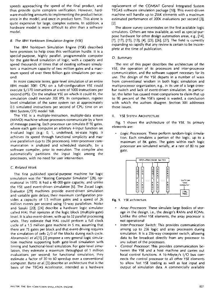
It. YSE SYSTEM ARCHITECTURE
Fig. 1 shows the architecture of the YSE. Its primary elements are:
Fig.
Logic Processors: These perform random-logic simula- tion. Each simulates a portion of the logic, up to a maximum of 8K gates. The gates within each logic processor are simulated serially, at a rate of 80 ns per gate.
INTER-PROCESSOR SWITCH
I L
0 0 L A L L
I II A
O R R G G I I
G R I A
c c C Y
P P P P R R R R 0 0 0 0 c c c c
. . . . . . t o / f r m host
computer
T T T T U
I . YSE architecture.
Array Processors: These simulate large bodies of stor- age in the design, i.e., the design’s RAMS and ROMs. Unlike the other YSE elements, the array processor is not operational Inter-Processor Switch: This provides communication among up to 256 logic and array processors during simulation. It is a 256-way crosspoint switch, allowing data to, be broadcast directly from any processor to any subset of the processors. Control Processor: This provides communication be- tween the YSE and a host machine and carries out local control functions. A 16-Mbyte/s 1/0 bus con- nects the control processor to all other YSE elements to allow fast YSE loading as well as fast input and output of simulation data. A commercially available
PFISTER THE I B M YORKTOWN S I M U L A T I O N ENGINE 851

microprocessor is embedded in the control processor to control YSE initialization, handle interrupts, run local YSE self-test, etc.
The YSE is built entirely from commercially available MSI components. Each logic processor contains roughly 750 chips and is build on a single multiwire board roughly 2 ft square. Two tubs, each containing 16 logic processors, fit into one standard 7-ft rack, providing a simulation capacity of 256K gates per rack. Two further racks are needed to hold a full 256-way crossbar switch.
Ill. THE LOGIC PROCESSOR
The logic processors are capable of three modes of logic simulation:
Unit delay: every gate has the same delay; a combina- torial net N levels deep takes N time units to stabilize. (The time unit referred to here is a simulation cycle, defined later.) Rank order: gates are linked together so that any depth combinatorial net stabilizes in a single time unit; memory cannot easily be modeled. Mixed mode: combinatorial nets are simulated in rank-order mode, and storage elements in unit-delay mode; a single time unit carries out one clock cycle of the simulated machine. In practice, virtually all use of the YSE is mixed mode.
The three modes of simulation are discussed below in functional terms. For a more detailed discussion of the logic processor design, see [IO].
A. Rank-Order Simulation
Fig. 2 shows the major elements contained in each logic processor, configured as used in rank-order simulation: data memory, instruction memory, and a logic unit.
F*EM)RI ~ I INSTRUCTION
( 8 K 12&if
Y words)
p-ziq LOG I C
LP7.J MEMORY
Fig. 2. Logic processor elements in the configuration for rank-order simulation,
The data memory contains 8K 2-bit words, each repre- senting a logic signal and holding its current state.
The instruction memory contains 8K 128-bit instruction words, each representing a single gate. Instructions contain four source addresses of data memory words, a destination address of a data memory word, and a logic function code. The latter is an address into a writable 32-element R A M (not shown) containing truth tables.
The logic unit obtains each instruction, gets the four
source data items, performs the indicated function on them, and deposits the result at the destination address in the data memory. This is the only operation performed: there are no branches, conditional instructions, etc. Thus a logic processor can only proceed from the first valid instruction to the last. Doing so is called performing a simulation cycle. Each of the instructions is executed in 80 ns, so a simulation cycle is completed in at most 655 p s . Since the YSE compiler attempts to spread the logic evenly across processors, the actual simulation cycle time is approxi- mately proportional to the amount of logic simulated, and inversely proportional to the number of processors.
The “logic unit” mentioned above i s actually a descrip- tive fiction: the logic function of each gate is realized by a simple R A M access that reads a value from a function table. Thus the YSE’s entire operation consists of little more than coordinated memory accesses, so much so that the YSE has been called “the world’s smartest memory.”
The lack of conditionals, branches, etc., allows the use of a deep pipeline in each logic processor without significant overhead, so logic processor speed is limited only by its internal storage bandwidth. This is increased by using mul- tiport memories: Four different data memory addresses are read simultaneously for each instruction.
In rank-order mode, instruction execution must obey an ordering: no gate’s instruction can be executed before those of its predecessor gates. This ordering is (roughly) by logical “rank” of a gate, giving rise to the term “rank-ordered simulation.” Since this ordering prohibits feedback, it is impossible to conveniently simulate memory. Unit-delay mode does not require such an order.
B. Unit- Delay Simulation
Fig. 3 shows the unit-delay simulation configuration. It is the same as the rank-order configuration, except that the data memory has been partitioned into two halves: “A“ memory and “6” memory. Each half holds the entire state
(8K 1 2 & i t MEMORY
words)
+ p-iq LOG i C
Fig. 3. Logic processor elements in the configuration for unit-delay simulation.
of the simulated machine, i.e., the state of each logic signal; thus the capacity of each processor is halved in this mode.
In unit-delay simulation, each successive simulation cycle alternates between two phases: read from “A,” write into “6” (shown in Fig. 3); and read from “6,” write into “A,” These modes are alternated, so the state of the simulated machine at time T in “A” is updated to an entire new state at time T + 1 in “B,” etc. The net effect is that each
85 2 PROCEEDINGS O F THE IEEE, VOL. 74, NO 6, JUNE 1986

simulation cycle performs a single gate delay for every gate in the entire simulated machine. A combinatorial network N levels deep requires N simulation cycles to settle.
All the instructions for all the gates of the design are executed in every simulation cycle, regardless of whether their input data are valid in a given cycle. The simulated system's clocks must be appropriately timed in terms of YSE simulation cycles to ensure that the intermediate, erro- neous, results are not stored in simulated registers. In rank- order simulation, by contrast, the partial order imposed on instruction execution allows any depth combinatorial net to produce valid results at the end of a single simulation cycle. In unit-delay mode, however, since no instruction's result affects any instruction's operation until the next simulation cycle, instructions may be executed in any order. Besides the important effect of allowing simulation of memory, this has important consequences for inter-processor communi- cation, as will be discussed later.
C. Mixed-Mode Simulation
It i s possible to mix the unit-delay and rank-order modes of operation. This "mixed" mode allows memory elements to be simulated in unit delay, while combinatorial logic between memory elements is rank ordered, thus providing fast simulation of sequential logic.
Mixed mode is actually a software convention. The YSE is run in unit-delay mode, but the source addresses of combi- natorial logic gates (only) are altered so that they always read from the "wrong" memory, thus using values com- puted in the same simulation cycle.
IV. INTER-PROCESSOR COMMUNICATION
Communication between YSE processors during simula- t ion is accomplished through the inter-processor switch, a full crosspoint switch. It consists of N switch ports, where N is the number of processors to be interconnected. As shown in Fig. 4, each switch port consists of a 256-way multiplexer and a switch memory that holds 8K 8-bit words. The address inputs of each port's multiplexer obtain data from the port's switch memory; and the logic unit of each processor is connected to a data input of every multiplexer. The output of each port's multiplexer is placed in the input memory of the port's associated processor. This memory is identical in form to the data memory.
The way the switch is used to communicate data be- tween processors, although simple, is slightly subtle. lt relies on the fact that all the processors operate synchro- nously, with a common clock and identical values in their program counters. Although the processors execute differ- ent instructions, all do their first, second, . - . , Kth, instruc- tions in lock step.
As each processor performs an instruction, the result it computes is sent to all the switch multiplexers. So at time K, each switch multiplexer has every processor's Kth result at i ts data inputs. Simultaneously, each switch memory's contents is read out sequentially in lock step with instruc- t ion execution. So at time K , each Kth switch memory location chooses the current (Kth) output of some logic processor and places it in each processor's input memory.
The switch memory contents, constant during a simula- tion, must be pre-established by compilation to create the correct communication pattern. This is discussed later.
Data from the switch are placed in the input memory sequentially, i.e., data from another processor's instruction K are put in input memory location K. The input and data memories are considered part of the same contiguous ad- dress space by logic processor instructions, so any instruc- t ion can access i t freely. In unit-dely mode, the input memory is divided like the data memory into A and B halves, and read/write access is alternated in phase with data memory access. As a result, there is no added inter- processor communication delay: All signals, external or in- ternal, are "delayed" by exactly one simulation cycle in unit-delay mode. In rank-order mode, input memory data can be validly accessed only after a pipeline delay. In mixed mode, "slow" (unit-delayed) signals suffer no additional delay, but "fast" (rank-ordered) signals suffer the pipeline delay.
Fig. 5 shows an example of communication among three processors. Note that at time 18, processor 3 in the figure is
.PROC I PROC 2 ,
SWITCH PORT "K" I LOGIC PROCESSOR "K"
I I I I t o input "K"
o f a i l switch 4 m u l t i p l e x e r s I
MEMORY SY I TCH I
words) MEMORY (8K & i t I -c DATA --c
INPUT MEMORY
from p r o c I from p r o c 2 words)
f r o m ' p i o c 2 5 6
(8K 2 - b i t -b-
I
Fig. 4. A switch port and its connection to a logic processor
Processor 1
A Y p - 1 A q - 1 A y 7 - 1
Processor 2 Processor 3
. . . SYITCH MEllORV CONTENTS 49 1 2 1
Fig. 5. Example of inter-processor communication: Note that at time 18, processor 3 in the,figure is both receiving information and sending it; and that processor 1 "fans out" to both processors 2 and 3.
both receiving information and sending it; and that processor 1 "fans out" to both processors 2 and 3.
Actually, each logic processor does not have to send to the switch the results of each instruction as i t is computed. There is a fifth source address in each logic processor
PFISTER THE I B M Y O R K T O W N S I M U L A T I O N ENGINE 853
instruction which selects a data (or input) memory value to send to the switch. This feature is used only when neces- sary to ameliorate the “scheduling problem” discussed in the section on the YSE compiler.
V. AN ARRAY PROCESSOR
Unlike other YSE elements described in this paper, all of which are currently operational, the YSE array processor is not. To indicate that there is no intrinsic problem with array simulation on the YSE, a possible array processor architec- ture will be sketched in this section. The YSE compiler contains operational code that supports this architecture.
The array processor consists of two parts: a parallel adapter (PAD), and a backing store processor (BSP).
A. The Parallel Adapter (PAD)
The function of the PAD is to collect array data from logic processors, passing them to the BSP; and distribute array data from the BSP to logic processors.
The PAD contains input and output memories, and an instruction memory. The input memory is identical in form to the input memory of a logic processor, and is loaded from the inter-processor switch in exactly the same way through a switch port.
Instructions are read from the instruction memory and executed in synchrony with logic processor instruction ex- ecution; PADS share with the logic processors the same program counter value.
Instruction memory words contain addresses in the input memory identifying on each instruction cycle the logic signals to be transferred to the BSP from input memory. They also contain control codes passed directly to the BSP, indicating:
whether the signals passed this cycle are valid, the type of data the signals represent (e.g., address,
which array is being addressed, what operation is to be performed (read or write).
If the array access was a read operation, the BSP will write data from the array into the PAD’S output memory. This will occur some number of instruction cycles after the read address has been transferred to the BSP and its oper- ation initiated. From the PAD output memory, data are passed to the inter-processor switch by use of an additional PAD instruction field that identifies a signal to be trans- ferred each instruction cycle.
B. The Backing Store Processor (BSP)
data to be written, write enable, etc.),
The BSP contains registers holding the array address, data to be written, and data read. It also contains an array descriptor memory and a large backing store.
Each word of the array descriptor memory describes one of the simulated arrays held in the backing store. An ad- dress in this memory is what the PAD passes to the BSP to identify an array. The array descriptor indicates the offset of the start of the array in the backing store, and the array’s stride (width of each simulated array word).
On receipt of a read or write command, the BSP uses the specified array descriptor to compute the backing store address of the desired word, and then performs the re- quested operation.
854
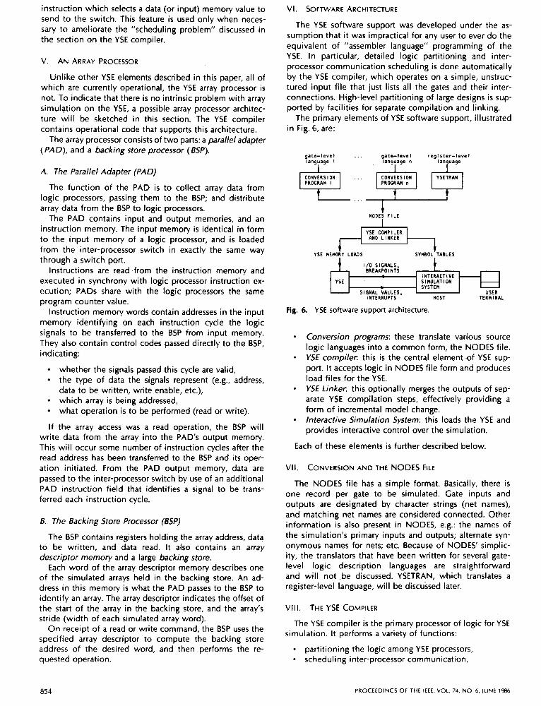
VI. SOFTWARE ARCHITECTURE
The YSE software support was developed under the as- sumption that i t was impractical for any user to ever do the equivalent of “assembler language” programming of the YSE. In particular, detailed logic partitioning and inter- processor communication scheduling is done automatically by the YSE compiler, which operates on a simple, unstruc- tured input file that just lists all the gates and their inter- connections. High-level partitioning of large designs is sup- ported by facilities for separate compilation and linking.
The primary elements of YSE software support, illustrated in Fig. 6, are:
g a t c l e v e l ... gate-level register-level language 1
I language n
I Ian uage 9
t ... S T ‘ t
NODES F I L E I
YSE COMPILER
1/0 SIGNALS,
SIMULATION SYSTEM
INTERRUPTS HOST TERM1 MAL
Fig. 6. YSE software support architecture.
Conversion programs: these translate various source logic languages into a common form, the NODES file. YSE compiler: this is the central element of YSE sup- port. It accepts logic in NODES file form and produces load files for the YSE. YSE Linker: this optionally merges the outputs of sep- arate YSE compilation steps, effectively providing a form of incremental model change. Interactive Simulation System: this loads the YSE and provides interactive control over the simulation.
Each of these elements is further described below.
VII. CONVERSION AND THE NODES FILE
The NODES file has a simple format. Basically, there is one record per gate to be simulated. Gate inputs and outputs are designated by character strings (net names), and matching net names are considered connected. Other information is also present in NODES, e.g.: the names of the simulation’s primary inputs and outputs; alternate syn- onymous names for nets; etc. Because of NODES simplic- ity, the translators that have been written for several gate- level logic description languages are straightforward and will not be discussed. YSETRAN, which translates a register-level language, will be discussed later.
VIII. THE YSE COMPILER
The YSE compiler is the priman/ processor of logic for YSE simulation. It performs a variety of functions:
partitioning the logic among YSE processors, - scheduling inter-processor communication,
P R O C E E D I N G S OF THE IEEE. VOL 74. N O . 6. JUNE 1 9 8 6

ordering instruction execution for rank-order simula- tion, creating symbol tables allowing access to logic values via the symbolic names that appeared in the NODES file.
Besides the NODES file, the compiler accepts a file which defines the logic functions to be simulated. This file also defines how the compiler should break down “macro gates:” gates with more than four inputs, or more than one output, which must be expanded into multiple instructions.
The compiler’s output is a group of files collectively called a module. Besides YSE load files, a module contains two symbol tables: a global symbol table, containing the names of primary inputs and outputs; and a local symbol table, containing all other net names.
A. The Scheduling Problem
A limitation of the YSE’s inter-processor communication method is that a processor can receive only one value from one other processor at each instruction time. Conflicts are therefore possible. For example, processor B could need signal values from both processor A and processor C. If both signal values are sent to the switch at the, same instruction time, processor B cannot get them both, as illustrated in Fig. 7(a).
processor processor processor A B C
i n s t r u c t i o n
( t i m e ) (a) address
Fig. 7. The scheduling problem: Time runs vertically in successive instruction executions. Both data items cannot be delivered to processor B at the same time (a). This can be solved (b) by moving all the instructions of processor C down one position and inserting a NOP. Since this may increase the simulation cycle length, it is better to try to f i l l in the NOP slot with an instruction that does not do inter-processor communication (c).
This problem is avoided by ordering instructions across processors appropriately. Finding an appropriate ordering has been called the scheduling problem. Solving it is a primary task of the YSE compiler.
If the logic processors are to hold sufficiently fewer gates than their maximum capacity, the scheduling problem can always be solved. How this can be done is illustrated in Fig. 7(b). Starting at the conflicting instruction location, the instructions of one of the conflicting source processors are
moved down one location and a null-operation instruction (NOP) is inserted. This moves the communication, eliminat- ing the conflict, but also lengthens the simulation cycle by one instruction. This lengthening can be avoided if one of the instructions after the conflict can be repositioned into the NOP slot, as illustrated in Fig. 7(c). The efficiency of inter-processor communication is measured by how often such repositioning is successful, i.e., how little the mini- mum simulation cycle length must be extended by the insertion of NOPs to avoid conflicts.
When all or part of the simulation is rank-ordered, there is an additional source of possible inefficiency. In unit- delay mode, i t is adequate for a processor to simply receive all required signals at any time in the simulation cycle. In rank-order mode, signals must be received early enough to be used by the instructions requiring them. Again, delaying destination rank-ordered gates by NOP insertion will al- ways work, given sufficient room. The extent to which other instructions can be repositioned to fill the NOP positions determines the overall efficiency.
The methods actually used for partitioning and schedul- ing, and experimental results, are described below.
B. Partitioning
Partitioning consists of assigning each instruction (gate) in the NODES file to a processor. The “scheduling problem” is really a partitioning problem: a partition of the logic that has little inter-processor communication allows a simple scheduling algorithm (a “greedy“ algorithm) to suffice.
It has been found experimentally that very simple parti- tioning algorithms work adequately for unit-delay simula- t ion in cases of interest. An initial preliminary algorithm, for example, simply placed the first N gates in processor 1, the next N in processor 2, etc., with N chosen to spread the load evenly. This actually worked: logic test cases from actual product designs could be scheduled in unit-delay mode without conflicts in the minimum number of instruc- t ion cycles. But while such a trivial partitioning algorithm may work for some cases, their dependence on NODES file order makes them dangerous; so two other algorithms are currently used.
The first algorithm currently used traces back through the logic from primary simulation outputs, attempting to place both a gate and its predecessors in the same processor. This requires essentially the same run time as the trivial al- gorithms, works at least as well for unit delay simulation, and produces adequate results for rank-order and mixed modes.
The second algorithm was devised in reaction to poor performance of the first on an abnormally bad test case. (The section on results includes this as case 1.) It optimizes the partitioning of gates among processors using a Monte Carlo technique called simulated annealing [16]: random peturbations are made to the partition, and the probability of accepting a bad change is gradually decreased. This algorithm requires approximately double the compute time of the first algorithm (trace back), but produces better results in difficult cases.
C. Scheduling
Scheduling consists of assigning each instruction a loca- tion within the processor assigned by partitioning. It also
PFISTER THE IEM Y O R K T O W N S I M U L A T I O N ENGINE 855

computes the contents of switch memory needed to per- form the inter-processor communication required by the chosen partition. As mentioned above, a rather simple “greedy” algorithm is used, as described below.
First all the instructions are sorted, using two keys:
Major key: rank-ordered gate level, defined as the maximum number of levels of logic between a gate and the first occurrence of a unit-delayed signal. Crossings between processors by rank-ordered signals are counted as additional logic levels. Instructions whose outputs are unit-delayed have a level of 0, and loops not broken by a unit-delayed signal are trapped as errors. Minor key: number of processors using the output of the instruction.
All the processors are then logically filled with NOP instructions, and each gate is processed in sorted order. The instruction memory of the gate’s assigned processor is scanned, starting at the lowest empty (NOP) location. The gate is placed at the first empty location satisfying all its constraints:
1) Communication constraint: All of the processors which must receive the result from this gate must be free; i.e., they must not already have been scheduled to receive another result.
2) Rank-order constraint: All necessary rank-ordered in- put data must be available to the gate, taking into account pipeline delays in receiving data from the other processors.
Rank-ordered groups of gates that cross processor boundaries tend more than any other factor to introduce unfilled NOP slots when they are first positioned. Restart- ing the scan from the first empty location tends to inter- leave such groups, since NOP locations left by one group are often usable by another. Processing the gates in a globally sorted order, without respect to assigned processors or rank-ordered group, makes immediate use of this inter- leaving and leaves few empty locations during scheduling.
IX. THE YSE LINKER
The YSE compiler can accept a maximum of 32K gates in a single compilation. Larger simulations are built by using the YSE linker to connect separate compilations. The linker connects gate inputs and outputs across compilations, re- solving inter-module scheduling, and combines the global symbol tables of the modules linked.
In doing inter-module scheduling, the linker uses the fifth source address mentioned in the section on “lnter- processor Communication.” The compiler does not use this feature. The reason is that the compiler can (and must) order each instruction anyway, and has not needed this facility. Were the linker to schedule by reordering instruc- tions, its operation would amount to a nearly complete recompilation of all the modules linked.
X. THE INTERACTIVE SIMULATION SYSTEM
The interactive simulation system loads the YSE and pro- vides interactive simulation control under the Conversa- tional Monitor System (CMS) of the IBM Virtual Machine/ System Product (VM/SP). Besides a YSE simulation module from the YSE compiler, the system also accepts files of data
defining initial array contents (e.g., for ROM personaliza- tion). The output of this system is primarily interactive display, but it also can dump array contents. This provides a batch trace capability when coupled with added simulated logic which stores traced data in simulated arrays. The system also provides a macro facility allowing groups of commands, with program logic, to be created by a user.
XI. YSETRAN
YSETRAN converts a register-level logic description to NODES, a gate-level description. The number of “gates” (YSE instructions) created by YSETRAN has proven to be between 4.5 and 7 times fewer than a manual design of the same logic. Since YSE simulation speed is proportional to the number of gates simulated, YSETRAN effectively pro- vides functional simulation on the YSE with a speedup of 4.5 to 7. (This additional “YSETRAN factor” was not in- cluded in the introductory estimates of 3081 simulation speed.)
YSETRAN’s ability to produce fewer gates than a manual design derives from the fact that YSE “gates” (instructions) are a very powerful “implementation technology.” For ex- ample, every gate has infinite fanout; every gate is implicitly dual-rail; and the functions available are very powerful: a 4-input exclusive-OR is one ”gate,” as is an enabled shift- register latch, etc.
YSETRAN initially does a simple and inefficient transla- t ion of the register-level specification to gate-level logic, without any attempt at optimization. This translation is very similar to that done in the proof technique described in [25]. In YSETRAN, this translation is followed by a heuristic optimizer which repetitively applies simple, local reduc- tions to the logic: e.g., propagate constants, collapse gate trees in 4-input gates, remove inverters by assuming dual-rail availability, etc. The only global operation performed is duplicate gate removal, accomplished with a fast hashing technique. These reductions are similar in spirit to those performed for logic synthesis [9]. They result in a reduction of the design to a locally optimized collection of ANDS, ORS,
and exclusive-ORs, with some higher level blocks (such as register latches) that were inserted during the original trans- lation.
When the simple reductions no longer change the logic, an attempt is made to collapse the logic further into higher function blocks, e.g., a pair of 2-input ANDS feeding a 2-input OR. The internal block organizations are compared with subnetworks of the logic, and when a match is found a replacement is performed. The results of this “block packing” vary greatly with the design being processed, but reductions in logic block count by a factor of two are not uncommon.
XI I . RESULTS
A. Goals
In distributing processing among multiple processors, the goal of the YSE is different from that of many multi- processor efforts. The usual goal (e.g., in [Ill) is to reduce the run time of a given problem by distributing the processing as widely as possible.
The primary purpose of parallelism in the YSE, on the
856 PROCEEDINGS OF THE IEEE. VOL. 74, NO 6. JUNE 1%

other hand, is to increase capacity while maintaining a constant run time. Therefore, a major goal of partitioning and scheduling is to run a problem on the minimum number of processors. The capacity of a logic processor, and thus the maximum simulation cycle length, is limited; and techniques for avoiding switch conflicts use up that limited resource. In fact, we have never had a problem increasing the number of processors, up to 256: the run time has always decreased (although not linearly), and there was always room to absorb the scheduling overhead. O n the other hand, there have been problems fitting mod- els into the minimum number of processors.
Whether a model fits into the minimal number of processors is important because the cost of a YSE installa- t ion is strongly dependent on the number of logic processors needed. The speedup obtained by adding processors is of some interest, but i t is doubtful that a YSE installation will plan to utilize less that 25 percent of i ts capacity, which is what is implied by a speedup of four. For this reason, the results presented below for processor counts above 12 to 24 are of limited practicality despite their general interest.
B. Result Validity
It is important to note that the YSE is a completely deterministic machine. There are no probabilistic estimates, e g , of bus contention, data traffic, etc., whose actual values can be found only be execution on actual hardware: instructions all take the same time and are always per- formed; and switch contention is completely resolved at compile time. Given the machine cycle time, the time to actually run a simulation is completely known after compi- lation and linking.
C. Definition of Speedup
The result of compiler partitioning and scheduling for a range of processors are plotted as speedups for five test cases in Fig. 8.
The usual definition of speedup S ( P ) is the execution time on one processor divided by the execution time on f processors. So a linear speedup ( S ( P ) = P ) , indicated by the dashed line in the figure, is optimal. However, none of
10 1 0'
Number of Processon
Fig. 8. Log-log plot of speedup obtained for five test cases.
the test cases, and indeed no case of interest for the YSE, will fit into a single YSE processor. So the single-processor reference value used is effectively the execution time on an imaginary single YSE processor with memories large enough to hold the entire problem.
0 . Test Case Characteristics
All of the test cases were originally specified at the register-transfer level and processed through YSETRAN. Since i t i s expected that the YSE will be extensively used from such input, these results are valid. However, it is worth noting that YSETRAN output is generally more dif- ficult to partition and schedule than good equivalent manu- ally designed logic for two reasons:
1) Longer path lengths: YSETRAN makes little attempt to optimize logic path length, and uses constructs with long path lengths, such as ripple-carry adders. For example, Case 1 has a rank-order depth of 110 levels of logic. This makes linear speedup impossible for cases 1, 2, and 3, since the minimum cycle length is the number of levels.
2) Greater logic connectivity: YSETRAN's use of high- function logic blocks with unbounded fanout means that there are fewer blocks, more highly connected than in a equivalent manual design. This makes partitioning more difficult, and leaves fewer opportunities to interleave logic chains in scheduling.
Characteristics of each of the test cases are listed in Fig. 9.
CASE CONHENTS NODE LEVELS COUNT LOGIC GATE R O NAX
Fig. 9. Summary characteristics of the five test cases. ~~
The parameters that are not self-explanatory are:
Logic The function performed by the logic of the test case. The five cases are variants of two actual designs: proc, a fully functional 32-bit microprocessor design; and /-unit, a portion of the instruction decode and dispatch unit of a high-performance mainframe.
rank-order logic unbroken by a unit delay point.
RO Max Levels: The length of the longest chain of
E. Discussion of the Results
The overhead is often zero, and always less than 10 percent, for all cases within a factor of 2 of the minimum number of processors needed. Within a factor of 4, i t reaches 30 percent for the two worst cases and is insubstan- tial for the others (see Fig. IO).
Cases 1 and 2 are roughly equivalent, despite the much larger number of rank-order levels in case 1, while case 3 does noticably better than both. This suggests that the global topology of a logic design is more important to its partitioning and scheduling than is the maximum number of levels, since case 3, in addition to having the fewest rank-order levels, is a globally more parallel logic design.
PFISTER: THE I B M Y O R K T O W N S I M U L A T I O N E N G I N E 857

Numkr of Rccesw
Fig. 10. Relative overhead: Number of instructions over the minimum possible, as a percentage of the minimum possi- ble.
Cases 4 and 5 (unit delay) have better speedup than the rank-order cases because unit-delay logic is easier to sched- ule. This gain comes nowhere near compensating for the loss in speed due to unit-delay execution. Case 5 is better than case 4 because i t has roughly twice as much logic than case 4, making it easier to spread across a given number of processors.
Fig. 11 shows how much of the switch’s capacity is used in case 3 as a function of the number of processors. The
Number of PrDcessors
Fig. 11. Switch utilization for test case 3.
data plotted are
total number of signals received by all processors
(number of processors) x (simulation cycle length) ’
The denominator is the total number of signals that could be received i f every switch cycle were used. As the processor count rises, utilization increases to about 50 percent and then drops. Prior to the peak, scheduling is limited by switch contention; after the peak, it is instead limited by the interprocessor rank-order delay. The peak of 50 percent indicates that a less general switch might have been used, but the YSE’s switch is relatively inexpensive, as discussed in the next section.
The run time of the compiler, for the simpler partitioning method, is approximately 300 gates per second of CPU time on an IBM model 3081 processor, running under the Con- versational Monitor System (CMS) of the IBM Virtual Ma- chine/System Product (VM/SP). Less than 30 percent of this time is spent doing partitioning and scheduling; the remainder goes to input/output operations, creation and maintenance of the large symbol tables needed, and pars- ing the N O D E S file.
XIII. DISCUSSION
The design of the YSE departs in a number of ways from conventional wisdom in both logic simulation and multi- processor design. This section discusses these issues.
A. The Full Crosspoint Switch
Of the various data switching methods available, the YSE’s crossbar is both the most general and the most expen- sive. However, a full 256-way crosspoint, including power supplies, occupies two of a full-scale YSE’s 15 racks, or 13 percent of the total size. The switch is an even smaller frac- tion of the total cost, since that is dominated by the high-speed memories of the logic processors.
A low-cost crossbar switch of this size and speed is an anomaly. It is explained by two things: First, the data path is only 3 bits wide. Second, the switch control is very simple because the switching pattern is not dependent on run-time data, a direct result of the fact that the YSE does not use event-driven simulation (see Subsection XIII-C). If the switch had to receive and arbitrate communication defined only at run time, its control logic alone might well have exceeded the size of the entire current YSE switch.
Given the low relative cost of the YSE’s switch, whether its generality is warranted is moot.
B. Timing Simulation
Virtually all software gate-level simulators, most pro- posals for special-purpose simulation hardware, and indeed even the L S M [I41 (the YSE’s predecessor) have provision for modeling signal propagation delays through gates. A de- liberate decision was made not to include this in the YSE, in favor of fast, detailed simulation of logic function via mixed and rank-order simulation. The reason is that YSE will pri- marily be used in the context of the LSSD design disipline, which eliminates many detailed timing dependencies and allows the use of timing analysis [I21 to determine critical paths. Since timing analysis is a data-independent proof technique, whenever i t can be applied its use is preferable to any simulation technique.
C. Event Driving
Again, virtually all software logic simulators and pro- posals for special-purpose simulation hardware incorpo- rated event driving, a technique which limits simulation only to those elements that are currently active. It is val- uable because the number of active blocks is expected to be a small fraction of the total block count; estimates and measurements range from 5 percent [2] to 10 percent, resulting in a potential speed increase by a factor between 10 and 20. Since the YSE does not use event driving, i t would appear that its speed advantage would be degraded
858 PROCEEDINGS O F THE IEEE, VOL. 74, NO. 6, JUNE 1%
by this amount. Assuming that timing simulation is not required, as is true in the YSE’s context, the author dis- agrees.
First, he notes that the YSE‘s capacity and speed are in large part due to not using event driving. Event driving inherently introduces run-time data dependencies into both processing and communication: which gates are not simu- lated is data-dependent. How this drastically affects the switch has been discussed; equivalent effects complicating the logic processors also occur. In addition, the efficiency of pipelining is curtailed. This is supported by comparing the relative simplicity of the YSE with the event-driven architectures of other hardware simulators (e.g., [2], [3],
It may be true that only 5 percent of the YSE’s evaluations are useful in the unit-delay mode, but the YSE is nearly never used in that mode; and i t is questionable that the same is true in rank-order or mixed modes. It has been noted [8] that the speed increase typically claimed for event-driven simulation-a factor of 10 to 20-corresponds closely to the typical number of levels of logic between latches in digital designs. This suggest that the low average activity level being exploited by event driving has a primary source in the delay from level to level in the logic. This speculation is supported by data on the HAL machine [24]. This event-driven machine simulates logic blocks contain- ing an average of 75 gates. The absorption of multiple logic levels into these single blocks should decrease the effective number of levels between latches substantially, and i f the speculation is true, should raise the average activity level. This is in fact what happens: HAL performance estimates are based on an activity level of 66 percent, dramatically above the 5 to 10 percent usually claimed. This implies that if timing information is not desired, rank-order or mixed- mode simulation on the YSE may incorporate nearly all of the speed advantage claimed for event driving, while avoid- ing the associated overhead.
XIV. SUMMARY AND CONCLUSIONS
~41) .
The YSE project has demonstrated that a speed increase of several orders of magnitude can be achieved for gate-level logic simulation using a highly parallel, special-purpose machine. A functionally simple processing element i s used, and inter-processor communication is provided by a full crosspoint switch that is not a large fraction of the system size, even for 256 processors. Static, compile-time schedul- ing of inter-processor allows a large number of processors to be effectively used to increase simulation capacity without increasing simulation time. Fully automatic parti- tioning of the input logic among processors and scheduling of inter-processor communication produce very good re- sults for all cases of interest.
The most basic factor in the YSE design was leaving timing verification to a proof technique, a decision relying on a restricted design discipline. Given that, rank-order or mixed-mode simulation approaches event driving in ef- ficiency, allows using an otherwise improbable switch, and dramatically simplifies processor design. The result is many fast processors working with little degradation and a dramatic increase in simulation speed.
The speed and capacity of the YSE make it applicable in areas beyond traditional detailed logic simulation. These areas include whole system verification (including input/
output), microcode verification, eariy software develop- ment, and diagnostic verification. All can be performed on the detailed logic actually implementing the product, rather than on a higher level abstraction that cannot be proved correct. As this list begins to indicate, the quantitative capacity and speed increases provided by the YSE are so large that they can alter the way we perceive simulation as a tool. It has been reported that use of the LSM, the YSE’s predecessor, “takes simulators beyond the verification role they have played in the past and makes them an integral part of the VLSl design environment” [14].
O n a broader scale, one can ask whether the YSE is a special case, or whether i t can be viewed as an initial example of how large-scale parallelism can be applied to computationally intensive areas of VLSl design. In fact, rather straightforward analyses show the potential of paral- lel computation in very many areas of VLSl design automa- tion [21].
However, machines such as the YSE are large and com- plex when constructed on the scale necessary to solve real industrial design problems. Building special-purpose ma- chines on their scale for all the areas which could benefit from it is of very questionable practicality. The computa- tional simplicity and inherent massive parallelism of gate- level logic simulation, its importance, broad applicability- and perhaps most importantly its lack of definable comple- t ion criteria!-may in fact make i t a special case. Exploiting the parallelism inherent in many other VLSl design automa- tion areas may require instead the development and utiliza- tion of parallel engines that are general enough to be used for a wide variety of tasks, such as the RP3 [22], [5].
ACKNOWLEDGMENT
The basic architectural concept behind both the YSE and the L S M [I41 i s due to John Cocke. The YSE Logic Processor, Inter-Processor Switch, and portions of the Control Processor were designed and built by Monty Denneau. Eric Kronstadt and Mark Laff, with the author, were principals in the design of the YSE software. Eric Kronstadt implemented the YSE compiler and linker, and Mark Laff implemented the Interactive Simulation System.
Many others, unfortunately too numerous to mention individually, participated in the integrated hardware and software project that produced in YSE.
REFERENCES
M. Abramovici et a/., “A logic simulation machine,” in Proc. 79th ACM/IEEE Design Automation Conf., pp. 65-73. M. Abramoviciet a / . , “A logic simulation machine,” IEEE Trans. Computer-Aided Design, vol. CAD-2, pp. 82-94, 1983. R. L. Bartoet a / . , “Architecture for a hardware simulator,” in
1980. Proc. IEEE Conf. on Circuits and Computers, pp. 841-893,
T. Blank et al, “A parallel bit map processor architecture for DA algorithms,” in Proc. 78th Design Automation Conf., pp. 837-845, June 1981. W. C. Brantley, K. P. McAuliffe, and J. Weiss, “The RP3 processor-memory element,” in Proc. 7985 Int. Conf. on Parallel Processing, pp. 782-789 Aug. 1985. M. A. Breuer and K. Shamsa, “A hardware router,” J. Digital Syst., vol. 4, no. 3, Winter 1980. T. Burggraff, A. Love, R. Malm, and A. Rudy, “The IBM Los Catos logic simulation machine hardware,” in Proc. IEEE Int: Conf. on Computer Design: VLSl in Computers, Oct. 1983. J . Cocke, private communication.
PFISTER: THE I B M YORKTOWN SIMULATION ENGINE 859

[91
[I 41
[I 51
J. A. Darringer, W. H. Joyner, C. L. Wrman, and L. H. Trevillyan, “Logic synthesis through local transformations,” ISM ). Res. Devel., vol. 25, no. 4, pp. 272-280, July 1981. M. M. Denneau, “The Yorktown simulation engine,” in Proc. 79th ACM/IEEE Design Automation Conf., pp. 55-59, 1982. E. F. Gehringeret a/ . , “The CM* tested,” Computer, vol. 15, no. 10 pp. 40-53, Oct. 1982. R. B. Hitchcocket a/ , “Timing analysis of computer hard- ware,” ISM). Res. Devel., vol. 26, no. 1, pp. 100-105, 1982. S. J. Hong and R. Nair, “Wire-routing machines-New tools for VLSl physical design,” Proc. IEEE, vol. 71 no. 1, pp. 57-65, Jan. 1983. J. Howard, R. Malm, and L. Warren, “Introduction to the IBM Los Catos logic simulation Machine,” in Proc. IEEE Int. Conf. on Computer Design: VLSl in Computers, Oct. 1983. J. Howard, R. Malm, and A. Rudy, “Using the IBM Los Catos logic simulation machine,” in Proc. IEEE Int. Conf. on Com- puter Design: VLSl in Computers, Oct. 1983. S. Kirkpartick, C. D. Celatt Jr., and M. P. Vecchi, “Optimiza- tion by simulated annealing,” Science, vol. 220, pp. 671-680. J. Kohn, R. Malm, C. Meiley, and F. Nemec, “The IBM Los Catos logic simulation machine software,” in Proc. lEEE Int. Conf. on Computer Design: VLSl in Computers, Oct. 1983. 1. Lineback, “Logic simulation speeded with new hardware,” Electronics, pp. 45-46, June 16, 1982. M. Monachino, “Design verification system for large-scale LSI designs,“ ISM J . Res. Devel. vol. 26, no. 1, pp. 89-99, 1982. N. Noike, K. Ohmori, H. Kondo, and T. Sasaki, “A high speed
logic simulation machine,” in Spring 1983 COMPCON Dig. Papers, pp. 446-451, Mar. 1983. C. F. Pfister, “Parallel processing, special-purpose hardware, and design automation,” in A C M Computer Science Conf. Proc., Feb. 1983. G. F. Pfister, W. C. Brantley, D. A. George, 5. L. Harvey, W. J. Kleinfelder, K. P. McAuliffe, E. A. Melton, V. A. Norton, and J. Weiss, ”The IBM research parallel processor prototype (RP3): Introduction and architecture,” in Proc. 7% Int. Conf. on Parallel Processing, pp. 764-771 Aug. 1985. L. Seiler, “A hardware assisted design rule check architecture,” in Proc. 79th ACM/IEEE Design Automation Conf., pp.
T. Sasaki et a/., “HAL: A block level hardware logic simulator,” in Proc. 20th IEEE/ACM Design Automation Conf., June 1983. C. L. Smith et a/., “Boolean comparison of hardware and flowcharts,” ISM ). Res. Devel. vol. 26, no. 1, pp. 106-116, 1982. K. Ueda, T. Komatsubara, and T. Hosaka, “A parallel processing approach for logic module placement,” IEEE Trans. Computer-Aided Design, vol. CAD-2, no. 1, pp. 39-47, Jan. 1983. Valid Logic Corporation sales literature, Cupertino, CA. A. Van Ausdal, “Use of the Boeing computer simulator for logic design confirmation and failure diagnostic programs,” Advanced Astronautic Sci., vol. 29, pp. 573-594, June 1971. Zycad sales literature, Zycad Corp., 2828 Anthony Lane South, Minneapolis, MN 55418.
232-238,1982.
PROCEEDINGS O F THE IEEE. VOL. 74, NO. 6, JUNE 1 9 8 6