Embed Size (px)
Citation preview

1756 IEEE TRANSACTIONS ON ELECTRON DEVICES, VOL. 48, NO. 8, AUGUST 2001
IC-Compatible Two-Level Bulk MicromachiningProcess Module for RF Silicon Technology
Nga Phuong Pham, Pasqualina M. Sarro, Senior Member, IEEE, Kiat T. Ng, andJoachim N. Burghartz, Senior Member, IEEE
Abstract—This paper presents a novel two-level silicon bulk mi-cromachining for integration of radio-frequency (RF) devices. TheRF devices are fabricated at the frontside of Si (100) wafers usingconventional integrated circuit (IC) technology. A post-processingmodule is applied from the wafer backside with precise alignmentto the frontside. This module can provide a blanket ground planeat an optimum position beneath the wafer surface, a frontside con-tact from the wafer surface to that ground plane, and trenches tosuppress crosstalk through the conductive silicon by adding twomask levels. An extension to four masks allows for an integrationof large passive components beneath circuitry for a much reducedchip area, lowering chip size and cost. The feasibility of the novelpost-process module is demonstrated through the fabrication ofmicrostrip transmission lines, conductor-backed spiral inductors,trench-barriers against crosstalk through the conductive siliconsubstrate, and high-quality subsurface spiral inductors.
Index Terms—Crosstalk, lithography, microstrip, microwavedevices, RF transceiver, silicon micromachining, spiral inductor,three-dimensional integration.
I. INTRODUCTION
T HE STRONGLY emerging wireless communicationsmarket calls for a higher integration level of radio-fre-
quency (RF) components in order to be able to reduce cost andform factor. Access to such highly integrated and ultimatelysingle-chip transceiver solutions gives promise to widen theexisting markets and also open up new product areas. The enor-mous market volume in RF technologies today, however, tendsto hinder the transition from conventional planar integratedstructures to more advanced RF structures. Such innovativefeatures may be of advantage, and in cases indispensable, tofurther pursue high-level integration of RF functions as theoperating frequencies move upwards. Planar silicon technologyhas several shortcomings with respect to the integration of RFtransceivers. If one compares a conventional RF transceiver inhybrid technology to a monolithic silicon transceiver, one canidentify several bottlenecks:
1) microstrip transmission-lines are widely used on printedcircuit board (PCB) in hybrid systems, but microstrips arenot yet available in advanced silicon technology;
2) integrated spiral inductors are typically built over mod-erately doped silicon to minimize substrate losses. Only
Manuscript received November 30, 2000. This work was performed undersupport of the Dutch Technology Foundation STW (Project DMF.5051 atwww.stw.nl). The review of this paper was arranged by Editor G. Baccarani.
The authors are with the Laboratory of Electronic Components, Technology,and Materials, Delft University of Technology, DIMES, 2600 GB Delft, TheNetherlands (e-mail: [email protected]).
Publisher Item Identifier S 0018-9383(01)05740-9.
planar contacts, laterally spaced from the inductor, canbe provided to bias the conductive silicon substrate.This may lead to inconsistent inductor characteristics,depending on the impedance terminations [2];
3) crosstalk through the conductive silicon substrate is a se-rious concern, and at frequencies beyond 1 GHz even con-ventional silicon-on-insulator (SOI) does not provide asolution [3];
4) inductors and microstrip transmission lines, in particular,occupy large areas, which is not a major issue on PCB. Insilicon technology, however, chip area is very costly andlarge integrated passive components lead to high cost andlimit the form factor.
These issues are illustrated in Fig. 1(a)–(d).These bottlenecks have been addressed in various ways by
research groups. The main feature that is missing in silicontechnology to enable microstrip integration, as requested in 1),is a via-contact through the silicon substrate to a metallizedground plane at the wafer backside, while choosing an optimumwafer thickness [Fig. 1(a)]. Several groups have proposed waferthinning to a substrate thickness of 100–200m, which wouldallow for through-wafer vias, but would raise serious concernsabout wafer handling and stability during the manufacturingprocess [4], [5]. The significance of a well-defined groundunder a spiral inductor coil on silicon substrates in 2) hasnot been widely recognized yet. The lack will likely lead toa challenge in future RF circuit design, where the effect of asubstrate contact on a nearby inductor will have to be taken intoaccount [Fig. 1(b)]. Crosstalk, identified in 3) as a major issue,may be suppressed to some extend by using high-resistivitySOI (HRS-SOI) wafers [Fig. 1(c)]. Even though such substrateslikely lead to reduced crosstalk and to reduced substrate lossesin inductors, they are not yet available in 8-in wafer diameter,which is the standard today. Another concern with SOI is thepoor thermal conductivity of the buried oxide layer, which willbecome particularly crucial with the integration of transmitterpower amplifiers. Silicon-on-sapphire (SOS), in contrast,provides excellent crosstalk isolation and thermal conductivityas well, but still owes prove of large-scale manufacturability,even though this technology has been around for a longtime [6]. The concern of large-area consumption of on-chippassives [Fig. 1(d)], as mentioned in 4), has been addressed byapproaches to built passives as part of the chip package. Thisconcept is mainly of interest at lower gigahertz-frequencies,where, e.g., inductor values are large and the impedances of theinterconnects to those passives in the package play a relativelysmall role. At high-gigahertz frequencies the implementation
0018–9383/01$10.00 © 2001 IEEE

PHAM et al.: IC-COMPATIBLE TWO-LEVEL BULK MICROMACHINING PROCESS MODULE 1757
Fig. 1. Nonoptimized RF structures in bulk silicon: (a) signal line withoutRF ground; (b) spiral inductor with nearby planar ground contact; (c) adjacentcomponents coupled by RF crosstalk through the conductive Si substrate; and(d) large passives, e.g., spiral inductors, consuming excessive chip area.
of the RF passives in the package is likely not a realistic option,because relatively small inductance and capacitance values,of similar order as the interconnect parasitics, are needed. Inaddition, the issue of testing a transceiver that includes off-chippassives prior to the packaging presents a big problem.
For these reasons it appears to be advantageous, to modifysilicon technologies in a way, that the issues 1)–4) are properlyaddressed. Given the large product volumes in wireless com-munications today, it is easily understandable, that silicon man-ufacturers tend to refrain from any major modification of theirfabrication processes. The introduction of SiGe technology, justby adding a SiGe-base layer to the bipolar transistor structure inbipolar or BiCMOS processes, for instance, has taken ten yearsto arrive at large capacity manufacturing [7].
In this paper, we describe a novel post-process module thatallows one to add the features required in 1)–4) to any siliconfabrication process without any need for modification andwithout any perturbation of that process. The results presentedhere are based on conference publications at ESSDERC’2000and IEDM’2000 [8], [9]. In Section II, we explain the basicconcept of the post-process module. A detailed descriptionof the process flow of the module is given in Section III. InSection IV, the electrical results obtained by using various teststructures are presented and discussed, and conclusions followin Section V.
II. THE POST PROCESSMODULE
The concept of post-processing is frequently used in mi-crosystem technology, where in many areas the product volumeis too small to justify a dedicated fabrication process [10].RF applications point to the other extreme, with a similarconclusion though. The extremely high production volume incommunications technology today makes the chip manufac-turers very cautious in modifying their fabrication processes, asalready mentioned above. This provides an opportunity to usepost-processing concepts in order to add the desired RF featuresto a silicon fabrication process without an interference with theintegrated circuit (IC) processing. The advantage is, that sucha post-process module can be developed independently andadded to the IC fabrication process as high-volume throughputcapability has been established.
Fig. 2. Cross section of microwave structures that can be realized using themicromachining post-process module: (a) microstrip with micromachinedground plane, (b) integrated conductor-backed spiral inductor, (c) trenchisolation structure using two inductors to sense crosstalk, and (d) inductorfabricated at the bottom of the etched cavity at the backside of the wafer.
The illustrations in Fig. 2 show how the components at thewafer frontside, as depicted in Fig. 1, can be enhanced byetching and metallizing the wafer backside. In Fig. 2(a), it isillustrated, how a two-step silicon etching process and a blanketbackside metallization can add the desired ground plane tothe structure shown in Fig. 1(a). Such a spaced ground planewould also be useful to define a uniform ground underneath thespiral coil of the inductor in Fig. 1(b), as shown in Fig. 2(b).The deep cavities and the vias to the frontside in Fig. 2(a)and (b) can be combined to form a trench through the entiresilicon substrate [Fig. 2(c)], eliminating the crosstalk throughthe conductive silicon [Fig. 1(c)]. Finally, such post-processingcould be enhanced with patterning of the backside metal, sothat the large chip area occupied by the spiral inductors in a RFcircuit [Fig. 1(d)] can effectively be reduced by placing many,if not all, inductors beneath the frontside circuitry [Fig. 2(d)].Prior work has shown, that such stacking of spiral inductorsand circuits is not possible in conventional silicon processtechnologies [11].
A post-process module applied to high-performance RF-ICtechnology has to meet certain criteria. First, the total thermalbudget has to be very low so that the characteristics of thepresent active devices are not altered. Second, the waferfrontside has to be protected during post-processing and third,features on the wafer backside have to be sufficiently wellaligned to the features at the frontside. Finally, the wafers haveto maintain a mechanical stability and handling comparable tobulk silicon wafers to ensure manufacturability. This last issuebecomes particularly apparent in some existing post-processapproaches to RF applications. The local etching of the bulksilicon had previously been applied either from the waferbackside or through windows from the wafer frontside toremove bulk silicon under the spiral coil of an inductor inorder to reduce the losses of that RF component [12], [13].Those approaches, though effective in improving the inductorquality factor ( ), raise concerns about the stability of thewafers in a manufacturing environment, because the inductorsare built on very thin membranes. In the post-processingmodule, presented here, wafer stability and handling have beenachieved by keeping silicon membranes very thick. Sufficient
1758 IEEE TRANSACTIONS ON ELECTRON DEVICES, VOL. 48, NO. 8, AUGUST 2001
spacing of signal lines at the frontside to ground planes spaced100–200 m away, however, is required to minimize eddycurrent effects [14]. The fact, that the full wafer thickness ismaintained for a considerable fraction of the chip, providessuch a micromachined wafer with stiffness similar to that of asolid wafer [15], [16].
III. FABRICATION PROCESS
A novel micromachining process has been developed atthe DIMES silicon facility for the post-process module. Onlyprocess steps using standard IC equipment have been em-ployed. The process starts with the fabrication of the devicesat the wafer frontside. Silicon 4-in p-type (100) wafers with athickness of 525 m and resistivities of 15 -cm or 3000 -cmwere used. A 500-nm thick low-stress low-pressure chemicalvapor deposition (LPCVD) silicon nitride layer is depositedon both sides of the wafers. This layer acts as a masking layerfor the backside etching and, at the same time, as an etch-stoplayer during the final through-wafer silicon etch in KOHfrom the backside. A 1.5-m thick silicon oxide is depositedby plasma-enhanced chemical vapor deposition technique(PECVD) onto the frontside of the wafer. This layer is neededto isolate the metal lines from the substrate, i.e., as field dielec-tric layer. Contact holes are opened in this oxide (stopping onthe underlying nitride) by plasma etching. The first metal layer,Al/1%–Si, is then deposited by sputtering and is patternedsubsequently. Another isolation layer, a PECVD oxide, isdeposited and via-holes are opened, again by dry etching. Asecond metal layer is deposited and patterned. The inter-metaloxide is 2 m thick and the two metal layers are 2m and 4
m thick, respectively. At this point the frontside processingis completed, and the wafers are ready for the post-processbulk micromachining. The flow of the post-process module isschematically shown in Fig. 3.
A. Blanket Metal Process
For structures like trenches to reduce crosstalk and RFdevices with a blanket metal ground plane, as depicted inFig. 2(a)–(c), only two extra masks are required. An EV-420contact aligner, that is capable of front-to-backside opticalalignment with an accuracy of1 m, is used. The first mask,used to define the ground plane area, is patterned on theLPCVD silicon nitride layer [Fig. 3(a)]. After the dry etching ofthe exposed nitride layer, the wafers are immersed in a 33 wt.%KOH solution at 85 C. Under these conditions the etch-rate ofsilicon is about 1.4 m/min. A special holder is used to protectthe frontside metal structures from being attacked by the KOHsolution. The silicon etching is stopped (time stop) when theground plane is at the pre-defined distance (generally 130m)from the front surface [Fig. 3(b)]. A 500-nm thick PECVD isthen deposited as a masking layer for the next etching step.In order to transfer patterns to the bottom of the deep-etchedcavities (down to 400 m) a new lithographic process has beendeveloped. A thick positive photoresist, AZ4562, with modifiedcoating and soft bake process is sufficient to obtain a goodcoverage and uniformity over the deep cavities. The secondmask used to define the wafer-through vias or the isolation
Fig. 3. Process flow of the micromachining post-process module.
trenches is exposed and the nitride-masking layer in the openedwindows is removed by plasma etching [Fig. 3(c)]. The bulksilicon etching in the KOH solution is resumed until the siliconnitride layer on the frontside is reached [Fig. 3(d)]. Nitrideremoval by a maskless dry etching step followed by sputteringof 2–4 m Al/1%–Si will complete the process for structuresusing a blanket metallization on the wafer backside.
Microstructures that were realized using this process areshown in Figs. 4 and 5. The pattern transfer process in thedeeply etched grooves, trenches, or cavities presented themajor challenge. The resolution of the pattern transfer processin deep cavities is affected by several parameters, such as

PHAM et al.: IC-COMPATIBLE TWO-LEVEL BULK MICROMACHINING PROCESS MODULE 1759
Fig. 4. SEM images of micromachined structures: (a) top view and (b) crosssection (magnification 39� and 49�, respectively).
Fig. 5. Backside of a wafer after the final metallization step: (a) optical imageshowing several two-level micromachined structures with blanket metal and(b) SEM image (magnification 39�) of one such structure with 8-wafer-throughcontact holes.
resist thickness variation, size and shape of the cavities, etc.Several tests were carried out to investigate these effects andto search for the optimum process parameters. As indicated by
the result shown in Fig. 5, the uniformity is sufficient to insurea successful pattern transfer to the wafer and to form severalcontact holes within the same cavity. The close-up of such astructure [see Fig. 5(b)] clearly shows that even the structuresplaced very close to the cavity side walls and quite closelyspaced could be well patterned.
B. Patterned Backside Metal
In order to fabricate a spiral inductor at the bottom of a cavitya few more steps and two additional masks are required afterthe second bulk silicon etch-step is performed [Fig. 3(d)]. First,a 500-nm thick PECVD silicon nitride layer that will act as in-sulation layer is deposited in the etched cavities. Contact win-dows to the frontside are opened [Fig. 3(e)] by dry etching.The Al/1%–Si layer is sputtered over the cavities. Dry etchingof the metal and an alloy step complete the device fabrication[Fig. 3(f)].
The two additional masks used for these structures containpatterns that have to be transferred at the bottom of and acrossdeep (wafer thickness) cavities. Special care has to be taken withthe lithographic process and slightly different conditions areused for each mask step. The high-viscosity, high-transparencypositive photoresist AZ4562 has been chosen as a suitable re-sist for this purpose. The coating is carried out in a Convac spincoater that allows modification of the spinning program. Thewafers are placed in the HMDS vapor-priming chamber for 10min. Then the resist coating is applied with a spinning speed of500 r/min for 4 s and 3500 r/min for 36 s. The soft bake takesplace at 95 C for 3 min. This coating program results in a goodstep coverage and reasonable thickness uniformity over the deepcavities [16].
The effect of dimension and shape of the cavities on the re-sist uniformity has also been investigated. Better results are ob-tained for the larger rectangles or square cavities. The averageresist thickness at the bottom of 400-m cavities obtained bythis coating process is about 5m. The pattern is then trans-ferred to the resist coated cavities by an EV-420 contact alignerin the soft contact mode. The gap between the mask and the pho-toresist layer is basically the depth of the etched cavities. Thismeans that higher exposure energy is needed to expose the pho-toresist. An exposure energy of 375 mJ/cm2 is used to open etchwindows and contact windows [Fig. 3(c) and (e)] and a some-what lower value to pattern the metal [Fig. 3(f)]. After expo-sure, a development step is carried out in a solution of AZ400Kand DI water (1 : 4). In order to open the small contact holesin the small cavities, as depicted in Fig. 3(e), the exposure anddevelopment step is applied twice. This is necessary as the re-sist in these small and deep cavities is thicker than at the groundplane area and this approach is preferred to an increase in energydose as this would result in resolution loss. The exposure energydepends also on the pattern design. For example, the mask forpatterning the metal layer [Fig. 3(f)] has more open areas thanthe one used for the small contact openings [Fig. 3(e)]. For thisreason there is no need to increase the exposure time for themetal patterning.
Another aspect that has to be considered in this patterntransfer process is the loss of resolution. The loss of resolutionis caused by the diffraction at feature edges on the mask when

1760 IEEE TRANSACTIONS ON ELECTRON DEVICES, VOL. 48, NO. 8, AUGUST 2001
using the proximity mode [17]. When the distance between themask and the resist is about 400–500m (the depth of etchedcavities), the dimensions of patterned structures can differ fromtheir value at the layout level. This loss of resolution has to betaken into account when designing structures to be patterned inand across deep cavities. The loss of resolution can deform theshape of small patterned structures. Our previous experimentshave shown that rounding of the corners takes place, forwhich smaller squares will be rounded when patterned at thebottom of 300–400 m deep cavities. However, as the averagedimensions of the structures required for the integration ofRF components are often in the order of tens of micrometers,the loss of resolution is still acceptable for several types ofstructures. Moreover, once the photoresist coating processis optimized for uniformity and reproducibility, the loss ofresolution can be partly compensated while designing themask. In order to increase the density of these contact holesand reduce the size of the structures, a better resolution in thelithography process is required. Increased resist uniformityover the wafer, independently of the shape and position of thecavities, is necessary. The potential of a new coating technique,i.e., photoresist spray coating [18], is currently being evaluated.
In spite of the current limitation, the developed process issuitable to realize several microwave components. A typical ex-ample is the integration of a spiral inductor at the bottom of acavity [as illustrated in Fig. 2(d)]. In conventional Si processes,spiral inductors with a typical size of about m haveto be placed side by side with the active devices. The integra-tion of inductors at the backside of the wafer is very attractiveas this can substantially decrease the circuit density. SEM im-ages of such a spiral inductor after resist exposure and develop-ment and after aluminum etching are depicted in Fig. 6(a) and(b), respectively. The inductor is integrated at the bottom of a390- m-deep cavity and contacts are brought to the frontsidevia two through-wafer holes.
The quality factor of this inductor can be improved if onecan reduce the effect of the parasitic capacitance of the entirelymetallized vias. Thus the patterning of metal lines across thevias is a very attractive prospect [19]. Fig. 7 shows an example ofpatterned metal lines running from the backside to the frontsideof the wafer across the two-level micromachined cavities. Thesepreliminary results are rather promising and can be extendedto other application areas, such as integration of high-densitythree-dimensional interconnection structures.
IV. CHARACTERIZATION OF THEPOST-PROCESSMODULE
For the electrical characterization of the post-processed RFfeatures, shown in Fig. 2(a)–(d), special test structures were fab-ricated:
A. Microstrip Transmission Lines
A 30- m wide signal line was fabricated at the top metal layerover a blanket ground plane, which was positioned at 130-mdistance beneath the surface, to form a microstrip [Fig. 2(a)].For comparison, the same signal line was also built withoutthat ground plane, i.e., over nonmicromachined bulk silicon.
Fig. 6. SEM images of a spiral inductor at the bottom of a 390-�m-deep cavity(magnification�44): (a) after resist exposure and development and (b) after Aldry etching.
Fig. 7. Patterned metal lines (Al) running over and across the etched cavities(magnification�72).
The ground plane resulted from a 4-m thick aluminum deposi-tion over the micromachined wafer backside. The contact to thatground plane was brought to the wafer surface by a via-contact,as described earlier in Section III. HRS substrates were used inthis experiment. Both lines were characterized by-parametermeasurements, carried out by using an HP8110 network ana-lyzer up to 40 GHz. The parasitics of the contact pads were notde-embedded. The reflection ( ) and the insertion loss ( )of 1-mm long lines are shown in Fig. 8. The characteristic im-pedances of both lines were determined as45 . The insertionloss of the microstrip was considerably smaller than that of the

PHAM et al.: IC-COMPATIBLE TWO-LEVEL BULK MICROMACHINING PROCESS MODULE 1761
Fig. 8. Measured insertion loss (S ) and reflection coefficient (S ) of anintegrated microstrip and a signal line.
signal line without a ground plane (“signal line”). At a frequencyof 17 GHz, the insertion loss was as low as 3 dB/cm, which com-pares well with state-of-the-art results on HRS wafers, on whichthe signal line is isolated from the substrate by an oxide [20].
B. Conductor-Backed Inductors
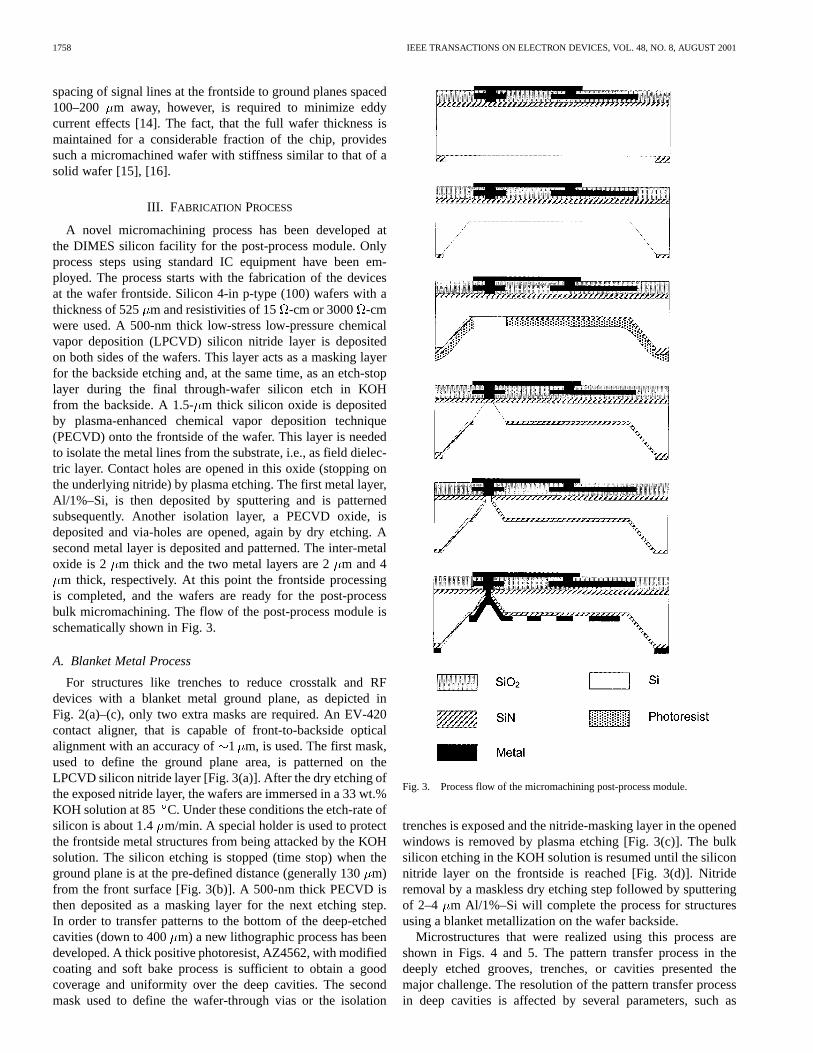
Test inductors with a ground plane underneath were built[Fig. 2(b)]. That ground plane was fabricated in the same wayas that of the microstrip, discussed above. It had been shown inearlier work, that an inductor without a ground plane can ex-hibit an “electrical asymmetry,” if a planar substrate contact isplaced in close vicinity to the inductor coil. The effect can beparticularly severe, if a ring of substrate contacts, a so-called“halo contact” surrounds the spiral coil [2]. The result of theeffect is, that its characteristics will depend on the impedanceterminations. It also means, that the same inductor tested inone-port and two-port test configurations will show differentcharacteristics. This results in the dilemma, that a lumped-el-ement model derived from a particular test site will not repro-duce accurately well in all possible circuit implementations. Wetherefore tested a 2.5-nH inductor with an underlying groundplane, an area of m , four turns, and conductorwidth and space of 13m each, in one-port and two-port config-urations. After measuring the-parameters up to 15 GHz andconverting to -parameters, the inductances and quality-factorswere computed as functions of frequency. The inductances werederived as , ,and and the quality-factors as
, ,and for the one-porttest and the two-port tests, respectively. Fig. 9 shows all mea-surement results in overlay. Very minor discrepancies were ob-served, demonstrating the effect of a uniformly defined groundpotential under the spiral coil. The fact, that the inductanceswere 2.5 nH, as targeted from design, shows that eddy currentsin the ground plane were negligible. That was a result of suffi-cient ground plane spacing of 130m [14].
C. Crosstalk Isolation
For the verification of crosstalk through the conductive sil-icon substrate laterally spaced spiral inductors were connectedto a two-port test structure. The insertion loss has been usedas an indication of crosstalk. The crosstalk has of course two
Fig. 9. Measured inductance (L) and quality factor (Q) of a four-turn spiralinductor with an area of226 � 226 �m extracted from one-port and bothtwo-port reflection parameters.
Fig. 10. Measured insertion loss (S ) for the different isolation structures.
components, i.e., electromagnetic coupling of the coils and ca-pacitive coupling through the silicon substrate. Four differenttest cases were considered. The silicon substrate resistivity was15 -cm in this experiment. First, the test structure was placedon a solid and floating silicon substrate to provide a control[Fig. 1(c)]. Second, a substrate contact ring was formed aroundone of the inductors to form a guard ring [3]. The third test struc-ture had a short trench barrier of 330m in length between thecoils [Fig. 2(c)]. For the fourth structure that trench had a lengthof 1.6 mm. The insertion losses measured for the four test struc-tures are shown in Fig. 10 up to 20 GHz. Obviously, the guardring did not provide an improvement compared to the controlstructure for frequencies above 3 GHz [3]. But the short trenchbarrier already resulted in an improvement of the crosstalk iso-lation by more than 30 dB. For the long trench the measurementwas limited by the noise floor of the test system, and one onlycan estimate that this crosstalk barrier provides an improvementof the isolation by 40 dB. It is obvious, that trenches etchedfrom the wafer backside up to the frontside provide very effec-tive crosstalk barriers and may thus be desirable additions to RFsilicon technologies.
D. Subsurface Spiral Inductors
Two experiments were carried out to demonstrate the fea-sibility of inductor integration underneath circuitry. First, testinductors were fabricated at a distance of 130m beneath thechip surface by using the post-process module with four mask
1762 IEEE TRANSACTIONS ON ELECTRON DEVICES, VOL. 48, NO. 8, AUGUST 2001
Fig. 11. Measured inductance (L) and quality factor (Q) of a two-turn inductorfabricated with a structure as in Fig. 2(d), with or without deembeding of theparasitic capacitance of via-cone and frontside pad.
levels, as described in Section III-B. The purpose of that experi-ment was to show, that those components can be integrated and,that the quality is not sacrificed in comparison to inductors posi-tioned at the chip surface. In a second experiment one inductorcoil was spaced from the wafer surface and a second coil was po-sitioned at the chip surface with maximum overlap of the buriedcoil. This structure thus formed a transformer, which representsthe worst-case for coupling between components at the surfaceand buried components.
Both structures were fabricated in a 15-cm silicon sub-strate. The subsurface test inductor occupied a total area ()of m , had a conductor width ( ) and space ()of 90 m and 40 m, respectively, and two turns ( ). Theresulting inductance was 3.4 nH. For simplicity reasons, this in-ductor was built with a via to the chip frontside that was fullymetallized (Fig. 6). The frequency-dependent inductance andquality-factor were derived from-parameter measurements, asdescribed in Section IV-B. The measurement results are shownin Fig. 11 for two cases, de-embedding of the probe pads onlyand de-embedding of probe pads and via. It becomes obvious,that for this relatively small inductor the fully-metallized viashave a significant impact on the inductor-. This is due to thelarge parasitic via capacitance as well as eddy current effects inthe metallized center area of the spiral coil [21]. Without an in-clusion of the via parasitic effects was determinedfor this 3.4 nH inductor. This high -value results to a largeextend from the thick backside metallization of 2m, but is cer-tainly affected considerably by the de-embedding of the largevia parasitic. The conclusion thus is that subsurface high-in-ductors can be integrated by using the post-process module, pro-vided that the via-capacitance can be reduced. Otherwise, thisprocess may best applicable to large inductors (10 nH). Oneway to reduce the parasitic capacitance of the via would be touse a lithographically defined metal line through the via insteadof fully metallizing it (Fig. 7; Section III-B). This, however, stilllimits the compactness of the spiral coil of the inductor, since ahollow coil design is required. Most effective would be to usean anisotropic dry etching of the via to reduce the surface area[5]. For the given spacing of the inductor coil from the chip sur-face an about ten-fold reduction of the via parasitic capacitancecan be expected. It should be noted here, that the inductor coil
Fig. 12. Measured insertion loss (S ) for two stacked coil pairs (turn ratios1 : 2 and 2 : 4).
was fabricated by using conventional contact printing. The con-sequence of this approach was that the features printed had tobe large. With a more sophisticated lithographic exposure it canbe expected, that conductor width and space can be more com-parable to structures built at the wafer frontside.
For the verification of the isolation between features at thefrontside and buried features, two transformer structures werebuilt. The first transformer had two turns at the frontside (
m , m, m, ) and oneturn in the buried coil ( m , m,
m, ), thus called 1 : 2 transformer. The secondtransformer had four turns at the frontside ( m ,
m, m, ) and two turns in theburied coil ( m , m, m,
), thus called 2 : 4 transformer. The insertion losses of thetwo transformers were measured both to be less than10 dB(see Fig. 12). This appeared to be good evidence of sufficientisolation of this worst-case coupling between frontside and sub-surface features. The isolation between circuitry and subsurfaceinductors is likely considerably better, but this needs ultimatelyto be demonstrated. The trend in those two test results, however,shows, that the isolation is better for smaller areas and fewernumbers of turns of the stacked coils. For very large subsurfaceinductors the distance to the chip surface may therefore have tobe somewhat increased.
V. CONCLUSION
A novel micromachining post-process module for RF silicontechnologies has been presented. The module provides severalunique feature that are not available in conventional silicon ICprocesses:
1) low-loss microstrip transmission lines can be integrated;2) conductor-backed inductors with characteristics indepen-
dent of the position of substrate contacts in the circuitlayout are feasible;
3) trench barriers between circuits and circuit sections be-come available to reduce on-chip crosstalk;
4) subsurface passive components can be employed to con-siderably reduce chip area and thus cost.
The post-process module is designed as a complement to any RFsilicon technology without interfering with the IC processing orperturbing any of the active device characteristics. It is, however,

PHAM et al.: IC-COMPATIBLE TWO-LEVEL BULK MICROMACHINING PROCESS MODULE 1763
most effective at moderate silicon substrate resistivities (10-cm), except for the crosstalk trench barrier becoming most
effective at high silicon conductivities, such as epi substrates forCMOS. At the given status, solely techniques compatible withIC processing have been employed, making the module natu-rally migratable to current silicon manufacturing facilities. Themodule is believed to be a considerable enhancement of currentIC processes without adding excessively to the total fabricationcost of a silicon RF chip.
ACKNOWLEDGMENT
All members of the DIMES IC-process group are gratefullyacknowledged for their help in processing the samples.
REFERENCES
[1] J. N. Burghartz, “Silicon RF technology—The two generic ap-proaches,” inProc 27th ESSDERC’97, Stuttgart, Germany, Sept. 1997,pp. 143–153.
[2] J. N. Burghartz, A. Ruehli, K. Jenkins, M. Soyuer, and D. Nguyen-Ngoc,“Novel substrate contact structure for high-Q silicon integrated spiralinductors,” inIEDM Tech. Dig., 1997, pp. 55–58.
[3] K. Joardar, J. Ford, and P. Welch, “A simple approach to modelingcrosstalk in integrated circuits,” inProc. BCTM, 1993, pp. 114–117.
[4] M. Luschas, M. Wollitzer, and J.-F. Luy, “Self-packaged mil-limeter-wave Si-IMPATT diodes,” inProc. Topical Meeting on SiliconMonolithic Integrated Circuits in RF Systems, 2000, pp. 95–98.
[5] J. Wu, J. Del Alamo, and K. Jenkins, “High-aspect-ratio silicon sub-strate-via technology and applications: Through-wafer interconnects forpower and ground and Faraday cages for SOC isolation,” inIEDM Tech.Dig., 2000, pp. 477–480.
[6] P. de la Houssaye, C. Chang, B. Offord, G. Imthurn, R. Johnson, P. As-beck, G. Garcia, and I. Lagnado, “Microwave performance of opticallyfabricated T-gate thin film silicon-on-sapphire based MOSFETs,”IEEEElectron Device Lett., vol. 16, pp. 289–292, June 1995.
[7] D. Harame, J. Comfort, J. Cressler, E. Crabbe, J. Y.-C. Sun, B. Meyerson,and T. Tice, “Si/SiGe epitaxial-base transistors. I. Materials, physics,and circuits,”IEEE Trans. Electron Devices, vol. 43, pp. 455–468, Mar.1995.
[8] N. P Pham, K. T. Ng, M. Bartek, P. M. Sarro, B. Rejaei, and J. N.Burghartz, “A micromachining post-process module for RF silicon RFtechnology,” inIEDM Tech. Dig., Dec. 11–13, 2000, pp. 481–484.
[9] N. Pham, P. Sarro, K. Ng, and J. Burghartz, “IC-compatible two-levelbulk-micromachining for RF silicon technology,” inProc. ESSDERC,2000, pp. 204–207.
[10] P. M. Sarro, “Sensor Technology Strategy in Silicon,”Sens. ActuatorsA, vol. 31, no. 1–3, pp. 138–143, 1992.
[11] J. Burghartz, D. Edelstein, M. Soyuer, H. Ainspan, and K. Jenkins, “RFcircuit design aspects of spiral inductors on silicon,” inISSCC Dig.,1998, pp. 246–247.
[12] J. Chang, A. Abidi, and M. Gaitan, “Large suspended inductors on sil-icon and their use in a 2-�m CMOS RF amplifier,”IEEE Electron De-vice Lett., vol. 14, pp. 246–248, May 1993.
[13] Y. Sun, H. van Zeijl, J. Tauritz, and R. Baets, “Suspended membraneinductors and capacitors for applications in silicon MMICs,” inProc.IEEE Microwave and Millimeter-wave Monolithic Circuits Symp., 1996,pp. 99–102.
[14] K. Ng, N. Pham, L. Sarro, B. Rejaei, and J. Burghartz, “Characteriza-tion of a bulk-micromachining post-process module for silicon RF tech-nology,” inProc. Topical Meeting Silicon Monolithic Integrated Circuitsin RF Systems, 2000, pp. 99–102.
[15] M. Bartek, “Mechanical integrity failure of bulk-micromachined Siwafers: Influence of structure geometry and wafer handling,” inProc.ASDAM 2000, Smolenice Castle, Slovakia, Oct. 16–18, 2000, ISBN0–7803–5939–9, pp. 227–230.
[16] N. P. Pham, P. M. Sarro, and J. N. Burghartz, “IC-compatible process forpattern transfer in deep wells for integration of RF components,”Proc.SPIE, vol. 4174, pp. 390–397, Sept. 2000.
[17] S. M. Sze,Semiconductor Devices Physics and Technology. NewYork: Wiley, 1985, p. 430.
[18] T. Luxbacher and A. Mirza, “Spray coating for MEMS, interconnectsand advanced packaging applications,”SENSORS, vol. 16, no. 7, pp.61–64, 1999.
[19] K. Herrick, J.-G. Yook, and L. Katehi, “Microtechnology in the devel-opment of three-dimensional circuits,”IEEE Trans. Microwave TheoryTech., vol. 46, pp. 1832–1844, Nov. 1998.
[20] A. Reyes, S. El-Ghazaly, S. Dorn, M. Dydyk, D. Schroder, and H. Pat-terson, “Coplanar waveguides and microwave inductors on silicon sub-strates,”IEEE Trans. Microwave Theory Tech., vol. 43, pp. 2016–2021,Sept. 1995.
[21] J. Lopez-Villegas, C. Cane, P. Losantos, and J. Bausells, “Improvementof the quality factor of RF integrated inductors by layout optimization,”IEEE Trans. Microwave Theory Tech., vol. 48, pp. 76–83, Jan. 2000.
Nga Phuong Phamwas born in Vietnam in 1973.She received the engineer degree in chemical engi-neering from Hanoi University of Technology, Hanoi,Vietnam, in 1994, the M.Sc. degree in materials sci-ence from Hanoi International Institute for MaterialsScience, Hanoi, Vietnam, in 1996. She is currentlypursuing the Ph.D. degree at Laboratory of ElectronicComponents, Technology, and Materials at the DelftUniversity of Technology, The Netherlands.
From 1997 to 1998, she worked was a ResearchAssistant in the group of “Surface and Inter-Surface
of Advance Materials” at the Centre Commisariat d’Atomique (CEA), Saclay,France. Since January 1999, she has been a Research Assistant with the Labo-ratory of Electronic Components, Technology, and Materials, Delft Universityof Technology. Her research focuses on MEMS technology for IC and RF com-ponents.
Pasqualina M. Sarro (M’84–SM’97) received theLaurea degree in solid-states physics from the Uni-versity of Naples, Italy, in 1980, and the Ph.D. de-gree in electrical engineering from the Delft Univer-sity of Technology, The Netherlands, in 1987. Herthesis dealt with infrared sensors based on integratedsilicon thermopiles.
From 1981 to 1983, she was a Post-doctoral Fellowin the Photovoltaic Research Group of the Divisionof Engineering, Brown University, Providence, RI,where she worked on thin-film photovoltaic cell fab-
rication by chemical spray pyrolysis. Since 1987, she has been with the DelftInstitute of Microelectronics and Submicron Technology (DIMES), Delft Uni-versity, where she is responsible for research on integrated silicon sensors andMEMS technology. Since April 1996, she has also been Associate Professor inthe Electronic Components, Materials, and Technology Laboratory, Delft Uni-versity. She has authored or coauthored more than 150 publications in refereedjournals and conference proceedings. She acts as reviewer for several tech-nical journals and has served as technical program committee member of theESSDERC Conferences (since 1995) and EUROSENSORS Conferences (since1999).
Kiat T. Ng received the B.Eng. (Hons.) degree, andthe M.Sc. degree, both in electrical engineering fromthe National University of Singapore, China, in 1995and 1998, respectively. Since 1998 he has been a Re-search Assistant pursuing the Ph.D. degree with theDepartment of Electrical Engineering, Delft Univer-sity of Technology, The Netherlands. His research in-terests are design and characterization of silicon RFcomponents.

1764 IEEE TRANSACTIONS ON ELECTRON DEVICES, VOL. 48, NO. 8, AUGUST 2001
Joachim N. Burghartz (M’90–SM’92) received theDipl. Ing. degree from the Technische HochschuleAachen, Germany, in 1982, and the Ph.D. degreefrom the University of Stuttgart, Germany, in 1987,both in electrical engineering.
From 1982 to 1987, he was with the University ofStuttgart where he developed sensors with integratedsignal conversion and a special focus on magnetic-field sensors. Between 1987 and 1998, he had beenwith the IBM T. J. Watson Research Center, York-town Heights, NY. His earlier research work at IBM
included applications of Si and SiGe epitaxial growth in high-speed transistordesign and integration processes, in which he was a member of the pioneeringteam that invented and developed IBM’s SiGe technology. From 1992 to 1994,he had a project leadership in a 0.15-�m CMOS development at IBM Micro-electronics, East Fishkill, NY. From 1994 to 1998, he concentrated on the de-sign of circuit building blocks for SiGe RF front-ends, with a special interestin high-quality passive components in silicon technology. He has been drivingthe integration and optimization of spiral inductors on silicon substrates, whichincluded a considerable number of patents and technical publications on thissubject. In November 1998, he moved to The Netherlands to take the positionof a Full Professor with teaching responsibilities in electrical engineering andmicroelectronic research at the research school DIMES at the Delft Universityof Technology. At DIMES, he is extending his research in RF silicon technologyto aspects ranging from novel materials to RF circuits. Since 1999, he has beenleading the DIMES research theme “High-Frequency Silicon Technologies forCommunications.” In March 2001, he became the Scientific Director of the re-search school DIMES. He has authored or coauthored more than 100 publi-cations in refereed journals and conference proceedings and he holds 12 U.S.patents.
Prof. Burghartz has served as Member of the program committees at the tech-nical conferences IEDM, ESSDERC, and BCTM. He was the BCTM GeneralChairman in 2000.


![TIMA Lab. Research Reportstima.univ-grenoble-alpes.fr/publications/files/rr/imf_209.pdfside bulk micromachining (FSBM) technology via the Circuit-Multi-Projects (CMP) service [19]](https://img.pdfslide.net/doc/110x75/60fc05318404fc3d24614e31/tima-lab-research-side-bulk-micromachining-fsbm-technology-via-the-circuit-multi-projects.jpg)