Embed Size (px)
Citation preview

IC TECHNOLOGY
By: Kanu Priya
COMPUCOM INSTITUTE OF TECHNOLOGY & MANAGEMENT,
JAIPUR (DEPARTMENT OF ELECTRONICS & COMMUNICATION)
Notes
IC TECHNOLOGY
(Subject Code: 7EC4)
Prepared By: Kanu Priya
Class: B. Tech.IV Year, VII Semester

IC TECHNOLOGY
By: Kanu Priya
SYLLABUS
UNIT 1 : INTRODUCTION TO TECHNOLOGIES- Semiconductor Substrate-Crystal defects, Electronic Grade Silicon, Czochralski Growth, Float Zone Growth, Characterization & evaluation of Crystals; Wafer Preparation- Silicon Shaping, Etching and Polishing, Chemical cleaning.
Beyond the Syllabus
Crystal structure
Crystallography
Learning Objectives
To provide a roadmap of basic microelectronic processing

IC TECHNOLOGY
By: Kanu Priya
NOTES UNIT WISE
IC TECHNOLOGY
·
UNIT-1
Introduction
The synthesis and purification of bulk polycrystalline semiconductor material represents the first step towards the commercial fabrication of an electronic device. This polycrystalline material is then used as the raw material for the formation of single crystal material that is processed to semiconductor wafers. The strong influence on the electric characteristics of a semiconductors exhibited by small amounts of some impurities requires that the bulk raw material be of very high purity (> 99.9999%). Although some level of purification is possible during the crystallization process it is important to use as high a purity starting material as possible.
Following oxygen (46%), silicon (L. silicis flint) is the most abundant element in the earth's crust (28%). However, silicon does not occur in its elemental form, but as its oxide (SiO2) or as silicates. Sand, quartz, amethyst, agate, flint, and opal are some of the forms in which the oxide appears. Granite, hornblende, asbestos, feldspar, clay and mica, etc. are a few of the numerous silicate minerals. With such boundless supplies of the raw material, the costs associated with the production of bulk silicon is not one of abstraction and conversion of the oxide(s), but of purification of the crude elemental silicon. While 98% elemental silicon, known as metallurgical-grade silicon (MGS), is readily produced on a large scale, the requirements of extreme purity for electronic device fabrication require additional purification steps in order to produce electronic-grade silicon (EGS). Electronic-grade silicon is also known as semiconductor-grade silicon (SGS). In order for the purity levels to be acceptable for subsequent crystal growth and device fabrication, EGS must have carbon and oxygen impurity levels less than a few parts per million (ppm), and metal impurities at the parts

IC TECHNOLOGY
By: Kanu Priya
per billion (ppb) range or lower.
Metallurgical-grade silicon (MGS)
The typical source material for commercial production of elemental silicon is quartzite gravel; a relatively pure form of sand (SiO2). The first step in the synthesis of silicon is the melting and reduction of the silica in a submerged-electrode arc furnace. An example of which is shown schematically in Figure 1, along with the appropriate chemical reactions. A mixture of quartzite gravel and carbon are heated to high temperatures (ca. 1800 °C) in the furnace. The carbon bed consists of a mixture of coal, coke, and wood chips. The latter providing the necessary porosity such that the gases created during the reaction (SiO and CO) are able to flow through the bed.
Figure 1.1: Schematic of submerged-electrode arc furnace for the production of metallurgical-grade silicon (MGS).
The overall reduction reaction of SiO2 is expressed in Equation 1, however, the reaction sequence is more complex than this overall reaction implies, and involves the formation of SiC and SiO intermediates. The initial reaction between molten SiO2 and C, Equation 2, takes place in the arc between adjacent electrodes, where the local temperature can exceed 2000 °C. The SiO and CO thus generated flow to cooler zones in the furnace where SiC is formed, Equation 3, or higher in the bed where they reform SiO2 and C, Equation 2. The SiC reacts with molten SiO2, Equation 4, producing the desired silicon along with SiO and CO. The molten silicon formed is drawn-off from the furnace and solidified.
(1)

IC TECHNOLOGY
By: Kanu Priya
(2)
(3)
(4)
The as-produced MGS is approximately 98-99% pure, with the major impurities being aluminum and iron however, obtaining low levels of boron impurities is of particular importance, because it is difficult to remove and serves as a dopant for silicon. The drawbacks of the above process are that it is energy and raw material intensive. It is estimated that the production of one metric ton (1,000 kg) of MGS requires 2500 - 2700 kg quartzite, 600 kg charcoal, 600 - 700 kg coal or coke, 300 - 500 kg wood chips, and 500,000 kWh of electric power. Currently, approximately 500,000 metric tons of MGS are produced per year, worldwide. Most of the production (ca. 70%) is used for metallurgical applications (e.g., aluminum-silicon alloys are commonly used for automotive engine blocks) from whence its name is derived. Applications in a variety of chemical products such as silicone resins account for about 30%, and only 1% or less of the total production of MGS is used in the manufacturing of high-purity EGS for the electronics industry. The current worldwide consumption of EGS is approximately 5 x 10⁶ kg per year.
Electronic-grade silicon (EGS)
Electronic-grade silicon (EGS) is a polycrystalline material of exceptionally high purity and is the raw material for the growth of single-crystal silicon. EGS is one of the purest materials commonly available, see Table 2. The formation of EGS from MGS is accomplished through chemical purification processes. The basic concept of which involves the conversion of MGS to a volatile silicon compound, which is purified by distillation, and subsequently decomposed to re-form elemental silicon of higher purity (i.e., EGS). Irrespective of the purification route employed, the fistep is physical pulverization of MGS followed by its conversion to the volatile silicon compounds.
A number of compounds, such as monosilane (SiH4), dichlorosilane (SiH2Cl2), trichlorosilane (SiHCl3), and silicon tetrachloride (SiCl4), have been considered as chemical intermediates. Among these, SiHCl3 has been used predominantly as the intermediate compound for subsequent EGS formation, although SiH4 is used to a lesser extent. Silicon tetrachloride and its lower chlorinated derivatives are used for the chemical vapor deposition (CVD) growth of Si and SiO2. The boiling points of silane and its chlorinated products are such that they are conveniently separated from each other by fractional distillation.
The reasons for the predominant use of SiHCl3 in the synthesis of EGS are as follows:
1. SiHCl3 can be easily formed by the reaction of anhydrous hydrogen chloride with MGS at reasonably low temperatures (200 - 400 °C);
2. it is liquid at room temperature so that purification can be accomplished using standard

IC TECHNOLOGY
By: Kanu Priya
distillation techniques; 3. it is easily handled and if dry can be stored in carbon steel tanks; 4. its liquid is easily vaporized and, when mixed with hydrogen it can be transported in steel
lines without corrosion; 5. it can be reduced at atmospheric pressure in the presence of hydrogen; 6. its deposition can take place on heated silicon, thus eliminating contact with any foreign
surfaces that may contaminate the resulting silicon; and 7. it reacts at lower temperatures (1000 - 1200 °C) and at faster rates than does SiCl4.
Chlorosilane (Seimens) process
Trichlorosilane is synthesized by heating powdered MGS with anhydrous hydrogen chloride (HCl) at around 300 °C in a fluidized-bed reactor, Equation 5.
(5)
Since the reaction is actually an equilibrium and the formation of SiHCl3 highly exothermic, efficient removal of generated heat is essential to assure a maximum yield of SiHCl3. While the stoichiometric reaction is that shown in Equation 5, a mixture of chlorinated silanes is actually prepared which must be separated by fractional distillation, along with the chlorides of any impurities. In particular iron, aluminum, and boron are removed as FeCl3 (b.p. = 316 °C), AlCl3 (m.p. = 190 °C subl.), and BCl(b.p. = 12.65 °C), respectively. Fractional distillation of SiHCl3 from these impurity halides result in greatly increased purity with a concentration of electrically active impurities of less than 1 ppb.
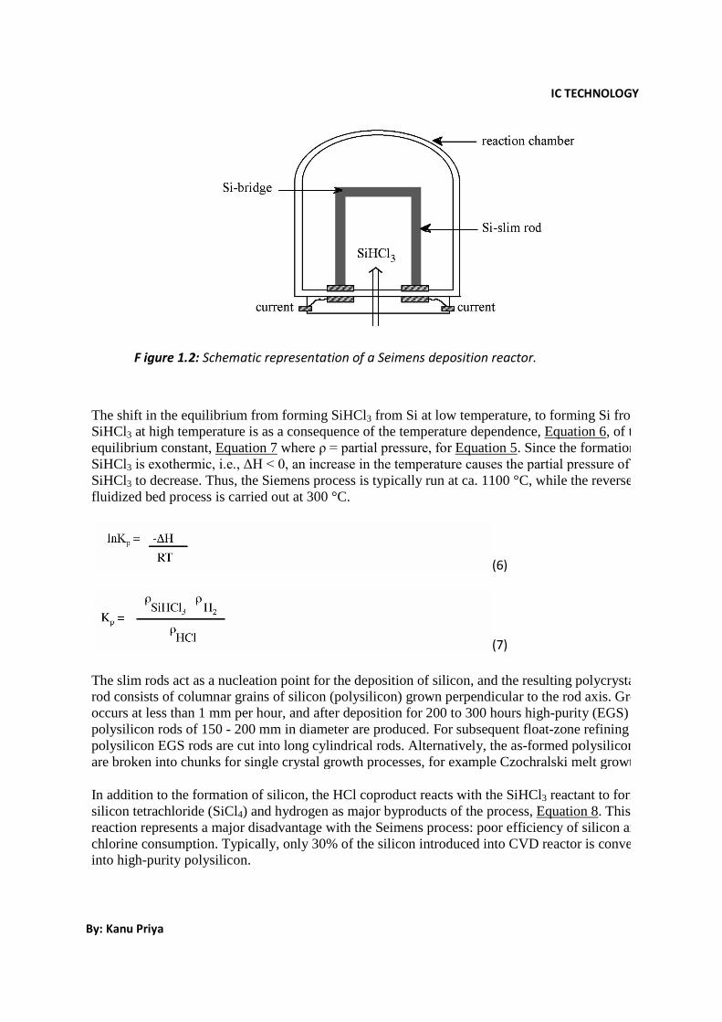
EGS is prepared from purified SiHCl3 in a chemical vapor deposition (CVD) process similar to the epitaxial growth of Si. The high-purity SiHCl3 is vaporized, diluted with high-purity hydrogen, and introduced into the Seimens deposition reactor, shown schematically in Figure 2. Within the reactor, thin silicon rods called slim rods (ca. 4 mm diameter) are supported by graphite electrodes. Resistance heating of the slim rods causes the decomposition of the SiHCl3 to yield silicon, as described by the reverse reaction shown in Equation 5.
IC TECHNOLOGY
By: Kanu Priya
F igure 1.2: Schematic representation of a Seimens deposition reactor.
The shift in the equilibrium from forming SiHCl3 from Si at low temperature, to forming Si from SiHCl3 at high temperature is as a consequence of the temperature dependence, Equation 6, of the equilibrium constant, Equation 7 where ρ = partial pressure, for Equation 5. Since the formation of SiHCl3 is exothermic, i.e., ΔH < 0, an increase in the temperature causes the partial pressure of SiHCl3 to decrease. Thus, the Siemens process is typically run at ca. 1100 °C, while the reverse fluidized bed process is carried out at 300 °C.
(6)
(7)
The slim rods act as a nucleation point for the deposition of silicon, and the resulting polycrystalline rod consists of columnar grains of silicon (polysilicon) grown perpendicular to the rod axis. Growth occurs at less than 1 mm per hour, and after deposition for 200 to 300 hours high-purity (EGS) polysilicon rods of 150 - 200 mm in diameter are produced. For subsequent float-zone refining the polysilicon EGS rods are cut into long cylindrical rods. Alternatively, the as-formed polysilicon rods are broken into chunks for single crystal growth processes, for example Czochralski melt growth.
In addition to the formation of silicon, the HCl coproduct reacts with the SiHCl3 reactant to form silicon tetrachloride (SiCl4) and hydrogen as major byproducts of the process, Equation 8. This reaction represents a major disadvantage with the Seimens process: poor efficiency of silicon and chlorine consumption. Typically, only 30% of the silicon introduced into CVD reactor is converted into high-purity polysilicon.

IC TECHNOLOGY
By: Kanu Priya
(8)
In order to improve efficiency the HCl, SiCl4, H2, and unreacted SiHCl3 are separated and recovered for recycling. Figure 3 illustrates the entire chlorosilane process starting with MGS and including the recycling of the reaction byproducts to achieve high overall process efficiency. As a consequence, the production cost of high-purity EGS depends on the commercial usefulness of the byproduct, SiCl4. Additional disadvantages of the Seimens process are derived from its relatively small batch size, slow growth rate, and high power consumption. These issues have lead to the investigation of alternative cost efficient routes to EGS.
Figure 1.3: Schematic representation of the reaction pathways for the formation of EGS using the chlorosilane process.
Silane process
An alternative process for the production of EGS that has begun to receive commercial attention is the pyrolysis of silane (SiH4). The advantages of producing EGS from SiH4 instead of SiHCl3 are potentially lower costs associated with lower reaction temperatures, and less harmful byproducts. Silane decomposes < 900 °C to give silicon and hydrogen, Equation 9.
(9)
Silane may be prepared by a number of routes, each having advantages with respect to purity and production cost. The simplest process involves the direct reaction of MGS powders with magnesium at 500 °C in a hydrogen atmosphere, to form magnesium silicide (Mg2Si). The magnesium silicide is then reacted with ammonium chloride in liquid ammonia below 0 °C, Equation 10.
IC TECHNOLOGY
By: Kanu Priya
(10)
This process is ideally suited to the removal of boron impurities (a p-type dopant in Si), because the diborane (B2H6) produced during the reaction forms the Lewis acid-base complex, H3B(NH3), whose volatility is sufficiently lower than SiH4, allowing for the purification of the latter. It is possible to prepare EGS with a boron content of ≤ 20 ppt using SiH4 synthesized in this manner. However, phosphorus (another dopant) in the form of PH3 may be present as a contaminant requiring subsequent purification of the SiH4.
Alternative routes to SiH4 involve the chemical reduction of SiCl4 by either lithium hydride, Equation 11, lithium aluminum hydride, Equation 12, or via hydrogenation in the presence of elemental silicon, Equation 13 - Equation 16. The hydride reduction reactions may be carried-out on relatively large scales (ca. 50 kg), but only batch processes. In contrast, Union Carbide has adapted the hydrogenation to a continuous process, involving disproportionation reactions of chlorosilaneEquation 14 - Equation 16, and the fractional distillation of silane, Table 3.
(11)
(12)
(13)
(14)
(15)
(16)
Pyrolysis of silane on resistively heated polysilicon filaments at 700 - 800 °C yields polycrystalline EGS. As noted above, the EGS formed has remarkably low boron impurities compared with material prepared from trichlorosilane. Moreover, the resulting EGS is less contaminated with transition metals from the reactor container because SiH4 decomposition does not cause as much of a corrosion problem as is observed with halide precursor compounds.
Granular polysilicon deposition
Both the chlorosilane (Seimens) and silane processes result in the formation of rods of EGS. However, there has been increased interest in the formation of granular polycrystalline EGS. This

IC TECHNOLOGY
By: Kanu Priya
process was developed in 1980’s, and relies on the decomposition of SiH4 in a fluidized-bed deposition reactor to produce free-flowing granular polysilicon.
Tiny silicon particles are fluidized in a SiH4/H2 flow, and act as seed crystal onto which polysilicon deposits to form free-flowing spherical particles. The size distribution of the particles thus formed is over the range from 0.1 to 1.5 mm in diameter with an average particle size of 0.7 mm. The fluidized-bed seed particles are originally made by grinding EGS in a ball (or hammer) mill and leaching the product with acid, hydrogen peroxide, and water. This process is time-consuming and costly, and tended to introduce undesirable impurities from the metal grinders. In a new method,large EGS particles are fired at each other by a high-speed stream of inert gas and the collision breaks them down into particles of suitable size for a fluidized bed. This process has the main advantage that it introduces no foreign materials and requires no leaching or other post purification.
The fluidized-bed reactors are much more efficient than traditional rod reactors as a consequence of the greater surface area available during CVD growth of silicon. It has been suggested that fluidizedbed reactors require 1/5 to 1/10 the energy, and half the capital cost of the traditional process. The quality of fluidized-bed polysilicon has proven to be equivalent to polysilicon produced by the conventional methods. Moreover, granular EGS in a free-flowing form, and with high bulk density, enables crystal growers to obtain the high, reproducible production yields out of each crystal growth run. For example, in the Czochralski crystal growth process, crucibles can be quickly and easily filled to uniform loading with granular EGS, which typically exceed those of randomly stacked polysilicon chunks produced by the Siemens silane process.
Zone refining
The technique of zone refining is used to purify solid materials and is commonly employed in metallurgical refining. In the case of silicon may be used to obtain the desired ultimate purity of EGS, which has already been purified by chemical processes. Zone refining was invented by Pfann, and makes use of the fact that the equilibrium solubility of any impurity (e.g., Al) is different in the solid and liquid phases of a material (e.g., Si). For the dilute solutions, as is observed in EGS silicon, an equilibrium segregation coefficient (k0) is defined by k0 = Cs/Cl, where Cs and Cl are the equilibrium concentrations of the impurity in the solid and liquid near the interface, respectively.
If k0 is less than 1 then the impurities are left in the melt as the molten zone is moved along the material. In a practical sense a molten zone is established in a solid rod. The zone is then moved along the rod from left to right. If k0 < 1 then the frozen part left on the trailing edge of the moving molten zone will be purer than the material that melts in on the right-side leading edge of the mmolten zone. Consequently the solid to the left of the molten zone is purer than the solid on the right. At the completion of the first pass the impurities become concentrated to the right of the solid sample. Repetition of the process allows for purification to exceptionally high levels

IC TECHNOLOGY
By: Kanu Priya
This section gives an overview of the integrated circuit technology. Semiconductor devices and circuits are formed in thin slices of a material (called a wafer) that serves as the substrate. For proper operation of the device/circuit, the substrate material must have crystalline structure where all the atoms are aligned in a specific pattern. In the first section of this chapter, the structure and growth of crystals are discussed. The next section deals with the cleaning of wafers which is an important step in the fabrication of integrated circuits. One of the basic building blocks in integrated circuit processing is the ability to deposit thin films of material. A large number of deposited films by wide variety of techniques are used in integrated circuits. These films can either be grown on semiconductor or deposited by various techniques. Most films can be formed by more than one method. Thermal Oxidation of Silicon is taken up first because it is an important step which is often repeated throughout the IC fabrication. This is followed by other principal film deposition techniques such as vacuum evaporation, sputtering and chemical vapor deposition. The properties of the films or substrate can be modified by process like diffusion and ion implantation and they enable to form a variety of devices in integrated circuits. A brief description of diffusion and implantation process and systems are given in section 4. In the subsequent section the lithography process is treated. The basic approaches to CMOS fabrication such as the p-well, the n-well, the twin tub and silicon on insulator processes are discussed in section 6. Very brief discussion on the fabrication of passive components also included. This chapter ends with a discussion on latch up and technology related CAD issues. In summary, an integrated circuit process is usually a structured sequence of operations such as the ability to deposit/modify thin films on the substrate, to apply a patterned mask on the films by photolithographic process, and to etch the films selectively to form actual devices. 3.1
Crystal and Growth
The basic semiconductor materials used in chips are crystalline silicon. This section briefly discuss about the properties of semiconductor crystals and how silicon crystals are grown.
3.1.1Crystals
Solid materials are classified by the way the atoms are arranged within the solid. Materials in which
atoms are placed at random are called amorphous. Materials in which atoms are placed in a high ordered structure are called crystalline. Poly-crystalline materials are materials with a high degree of short-range order and no long-range order. These materials consist of small crystalline regions with
random orientation called grains, separated by grain boundaries. There three arrangements are summarized in Fig.3.1.
Up to the 150 mm wafer diameter era, wafers had flats, and the flats indicate the following information:
1. The doping type of the wafer (n- or p-type) 2. The orientation of the wafer: {100} or {111}
And wafers with diameters larger than 200 mm generally will have no flat at all, but just a small "notch" as shown in Fig. 3.9.

By: Kanu Priya
Fig. 1.4
Integrated circuits are built on singlepurity, a high degree of crystalline perfection, and high structure uniformity. Such silicon crystal preparation involves two major steps: (1) refinement of raw material (such as quartzite, a type of sand) into electronic grade polycrystalline silicon (EGS) and (2) growing of singleEGS either by Czochralski or Float Zone process
Fortunately, the raw Si is abundantly available from steel industry and only a small part of it is required for the semiconductor industry. Since it is a byproduct from steel industry, it is commonly called Metallurgical Grade Silicon (MGS). MGS is poly crystalline material withmade by the reduction of SiO2 (quartz sand) with carbon (coal) in huge furnaces lined with carbon, with big graphite electrodes inside (carrying huge amounts of current) at about 2000°C. The reaction is
C (s) + SiO2 (s) Si (l) + CO (g)
But care should be taken to suppress the other reaction occurring simultaneously (Si + C which will not only reduce the yield of Si, but clog up the furnace by SiC.
The 9N purity (99.9999999) silicon is made essentially in three steps:
Liquid Si reacts with all substances and is a universal solvent. This makes crystal growth from liquid Si somewhat difficult. Si is converted to SiHCl
Si (s) + 3HCl (g) SiHCl3 (g) + H
The resulting Trichlorosilane is already much purer than the raw Si; it is a liquid with a boiling point of 31.8°C.
The SiHCl3 is further distilled, resulting in extremely pure Trichlorosilane.
Finally, high-purity Si is produced by a "Chemical Vapor Deposition" (CVD) processlater sections) .
IC TECHNOLOGY
Fig. 1.4 Identification of wafers
Integrated circuits are built on single-crystal silicon substrates that possess a high degree of chemical purity, a high degree of crystalline perfection, and high structure uniformity. Such silicon crystal
major steps: (1) refinement of raw material (such as quartzite, a type of sand) into electronic grade polycrystalline silicon (EGS) and (2) growing of single-crystal silicon from this EGS either by Czochralski or Float Zone process
is abundantly available from steel industry and only a small part of it is required for the semiconductor industry. Since it is a byproduct from steel industry, it is commonly called Metallurgical Grade Silicon (MGS). MGS is poly crystalline material with a purity of about 99%. It is
(quartz sand) with carbon (coal) in huge furnaces lined with carbon, with big graphite electrodes inside (carrying huge amounts of current) at about 2000°C. The reaction is
But care should be taken to suppress the other reaction occurring simultaneously (Si + C which will not only reduce the yield of Si, but clog up the furnace by SiC.
The 9N purity (99.9999999) silicon is made essentially in three steps:
Liquid Si reacts with all substances and is a universal solvent. This makes crystal growth from liquid Si somewhat difficult. Si is converted to SiHCl3 via the reaction at around 300°C
(g) + H2 (g) + heat
osilane is already much purer than the raw Si; it is a liquid with a boiling point of
is further distilled, resulting in extremely pure Trichlorosilane.
purity Si is produced by a "Chemical Vapor Deposition" (CVD) process
IC TECHNOLOGY
crystal silicon substrates that possess a high degree of chemical purity, a high degree of crystalline perfection, and high structure uniformity. Such silicon crystal
major steps: (1) refinement of raw material (such as quartzite, a type of sand) crystal silicon from this
is abundantly available from steel industry and only a small part of it is required for the semiconductor industry. Since it is a byproduct from steel industry, it is commonly called
a purity of about 99%. It is (quartz sand) with carbon (coal) in huge furnaces lined with carbon, with
big graphite electrodes inside (carrying huge amounts of current) at about 2000°C. The reaction is
But care should be taken to suppress the other reaction occurring simultaneously (Si + C SiC),
Liquid Si reacts with all substances and is a universal solvent. This makes crystal growth from liquid Si
osilane is already much purer than the raw Si; it is a liquid with a boiling point of
purity Si is produced by a "Chemical Vapor Deposition" (CVD) process (discussed in

By: Kanu Priya
Often very small but precisely measured amounts of As, P or B can also be incorporated into the growing polysilicon. The next step is to convert this polyused in this case; Czochralski or crucible grown crystals (CZ crystals) and Float zone (FZ) crystals. The FZ method produces crystals with the highest purity, but cannot be used to produce crystals with large diameters. Czochralski or crucible (CZ) met The Czochralski method, invented by the Polish scientist J. Czochralski in 1916, is the method of choice for high volume production of Si single crystals. A schematic drawing of a crystal growth by Czochralski method is given in Fig.3.10.
Essentially, a crystal is "pulled" out of a vessel containing liquid Si as shown in Fig 3.10. A seed crystal is dipped into the liquid and is subsequently slowly withdrawn from the melt. The pulling rate (usually a few mm/min) and the temperature profile dachieved. The solubility of impurity atoms in the melt is larger than in the solid. As a result, the crystal will be purer than the liquid and crystal growing is simultaneously a purification method. However the distribution of impurities vary along the length of a crystal and a homogeneous doping is difficult to achieve. Practically only As, P, and B are used for doping because of their segregation coefficient are close to 1. The segregation coefficient in thermof impurity atoms in the growing crystal and that of the melt. It is usually mucimpurity atoms prefer to stay in the melt. Oxygen is the most important impurity founmolten silicon is contained. The oxygen is typically at a level of about 5x10silicon. Oxygen has three principal effects in the silicon crystal. In an asgenerally occupies interstitial positions in the silicon lattice and improves the yield strength by 25%. A small amount of the oxygen in the crystdonors can be formed, which is significant to increase the resistivity of lightly doped PDuring the CZ growth process, the crystal cools slowly through ~500°C temperature and oxygen donors form.
IC TECHNOLOGY
Often very small but precisely measured amounts of As, P or B can also be incorporated into the growing polysilicon.
The next step is to convert this poly-Si to a single crystal. There are two methods for crystal growtused in this case; Czochralski or crucible grown crystals (CZ crystals) and Float zone (FZ) crystals. The FZ method produces crystals with the highest purity, but cannot be used to produce crystals with large
Czochralski or crucible (CZ) method of crystals growth
The Czochralski method, invented by the Polish scientist J. Czochralski in 1916, is the method of choice for high volume production of Si single crystals. A schematic drawing of a crystal growth by
Fig.3.10.
Essentially, a crystal is "pulled" out of a vessel containing liquid Si as shown in Fig 3.10. A seed crystal is dipped into the liquid and is subsequently slowly withdrawn from the melt. The pulling rate (usually a few mm/min) and the temperature profile determines the crystal diameter that can be achieved. The solubility of impurity atoms in the melt is larger than in the solid. As a result, the crystal will be purer than the liquid and crystal growing is simultaneously a purification method. However the istribution of impurities vary along the length of a crystal and a homogeneous doping is difficult to
Practically only As, P, and B are used for doping because of their segregation coefficient are close to 1. The segregation coefficient in thermodynamic equilibrium gives the relation between the concentration of impurity atoms in the growing crystal and that of the melt. It is usually much lower than 1 because
atoms prefer to stay in the melt.
Oxygen is the most important impurity found in silicon and is from the quartz crucible in which the molten silicon is contained. The oxygen is typically at a level of about 5x10¹⁷/cm3 silicon. Oxygen has three principal effects in the silicon crystal. In an as-grown crystal, the oxygen generally occupies interstitial positions in the silicon lattice and improves the yield strength by 25%. A small amount of the oxygen in the crystal forms SiO4 complexes and act as donors. Even 10donors can be formed, which is significant to increase the resistivity of lightly doped PDuring the CZ growth process, the crystal cools slowly through ~500°C temperature and oxygen
IC TECHNOLOGY
Often very small but precisely measured amounts of As, P or B can also be incorporated into the growing polysilicon.
Si to a single crystal. There are two methods for crystal growth used in this case; Czochralski or crucible grown crystals (CZ crystals) and Float zone (FZ) crystals. The FZ method produces crystals with the highest purity, but cannot be used to produce crystals with large
hod of crystals growth :
The Czochralski method, invented by the Polish scientist J. Czochralski in 1916, is the method of choice for high volume production of Si single crystals. A schematic drawing of a crystal growth by
Essentially, a crystal is "pulled" out of a vessel containing liquid Si as shown in Fig 3.10. A seed crystal is dipped into the liquid and is subsequently slowly withdrawn from the melt. The pulling rate
etermines the crystal diameter that can be achieved. The solubility of impurity atoms in the melt is larger than in the solid. As a result, the crystal will be purer than the liquid and crystal growing is simultaneously a purification method. However the istribution of impurities vary along the length of a crystal and a homogeneous doping is difficult to
Practically only As, P, and B are used for doping because of their segregation coefficient are close to 1. odynamic equilibrium gives the relation between the concentration
h lower than 1 because
d in silicon and is from the quartz crucible in which the 1018/cm3 in CZ
grown crystal, the oxygen generally occupies interstitial positions in the silicon lattice and improves the yield strength by 25%. A
complexes and act as donors. Even 1016 /cm3 donors can be formed, which is significant to increase the resistivity of lightly doped P-type wafers. During the CZ growth process, the crystal cools slowly through ~500°C temperature and oxygen

IC TECHNOLOGY
By: Kanu Priya
Typically annealing of the grown crystal is carried at temperatures above 500°C and to remove these oxygen complexes. The oxygen can precipitate under normal device processing conditions, forming SiO2 regions inside the wafer. The precipitation arises because the oxygen was incorporated at the melt temperature. Carbon is another impurity normally present in CZ grown silicon crystals. The carbon comes from the graphite components in the crystal pulling machine. For some applications, it is important to have even lower concentrations of impurity atoms like Oxygen and the Float Zone Crystal Growth is used.
Float Zone Crystal Growth The basic idea in float zone (FZ) crystal growth is to move a liquid zone through the material as shown in Fig.3.11. In this process the end of a long polysilicon rod is locally melted and brought in contact with a single crystalline Silicon seed. The melted zone slowly migrates through the poly rod leaving behind the final perfect crystal. In the float zone process, dopants and other impurities are rejected by the growing silicon crystal. Impurities tend to stay in the liquid and refining can be accomplished, especially with multiple passes. Since the melt never comes into contact with anything but vacuum (or inert gases), there is no incorporation of impurities by dissolving the crucible material as in the CZ crystal growth method. FZ crystals therefore are always used when very low oxygen concentrations are required. One needs to keep the liquid Si from just collapsing by surface tension and this limit the maximum diameter of crystals.
Fig.1.5 Czochralski method of crystal growth

IC TECHNOLOGY
By: Kanu Priya
Fig.1.6: Float Zone (FZ) method of crystal growth
Table 1.1 : Comparison of the CZ and FZ Growth Methods
Characteristic CZ FZ
Growth Speed (mm/min) 1 to 2 3 to 5
Crucible Yes No
Consumable Material Cost High Low
Heat-Up/Cool-Down Times Long Short
Axial Resistivity Uniformity Poor Good
Oxygen Content (atoms/cm3 ) >1x10 18 <1x10 16
Carbon Content (atoms/cm3 ) >1x10 17 <1x10 16
Metallic Impurity Content Higher Lower
Bulk Minority Charge Carrier Lifetime (s) 5-100 1,000-20,000
Production Diameter (mm) 150-200 100-150
Conversion of silicon ingots into polished wafer is carried out by shaping, slicing, lapping and edge grind, etching, polishing and cleaning operations. For many applications, the quality of a polished wafer is not sufficient mainly due to defects generated during crystal growth in the bulk of the wafer. The best solution to this problem is to deposit an additional layer of high purity Silicon on the top of a polished wafer substrate. This process is known as epitaxy. This has the additional advantage in that the electrical resistivity of the surface layer can be different than that of the substrate.

By: Kanu Priya
WAFER PREPARATION
It includes the following steps
(1)SILICON SHAPING
(2)ETCHING
(3)POLISHING
(4)CHEMICAL CLEANING
First step includes six machining operations
Silicon epitaxial deposition (epitaxy) refers to the process of growing a thin layer of singlesilicon over a single-crystal silicon substrate. Epitaxy is different from the Czochralski process in that the crystal can be grown below the melting point. In semiconductors, the deposited film is often the same material as the substrate, and the process is known as homodeposition over a silicon substrate. If the layer andAs on GaAs, the process is termed as heteroepitaxy (MBE) method where the physical transport of material is carried out to a heated substrate. In Vapor Phase Epitaxy, materials such as Si, Ga, As, dopants etc. are transported in the form of volatile compounds to the substrate, where they react to form the epitaxial layer.
There are four major chemical sources of silicon for commercial epitaxial deposittetrachloride (SiCl4), (2) trichlorosilane (SiHClThe over-all reaction for silicon epitaxy by silane reaction may be written as follows:
The growth of an epitaxial layer over the substrate offers some advantages. By growing a lightly doped epi layer over a heavily-doped silicon substrate, a higher breakdown voltage across the collectorsubstrate junction is achieved while maintaining low coallows a higher operating speed. By fabricating the CMOS device on a very thin (3epi layer grown over a heavily-doped substrate, latchimproving the performance of devices, epitaxy also allows better control of doping concentrations of the devices. The layer can also be made oxygenhigher cost of wafer fabrication, additional process complexities, in the epi layer.
In this section we have studied about the crystal structure, how it was grown and converted to wafers. The next section discusses the importance of wafer cleaning and different methods used to remove contaminations.
Etching
IC TECHNOLOGY
First step includes six machining operations like slicing ,lapping, edge countering etc.
Silicon epitaxial deposition (epitaxy) refers to the process of growing a thin layer of singlecrystal silicon substrate. Epitaxy is different from the Czochralski process in that
e crystal can be grown below the melting point. In semiconductors, the deposited film is often the same material as the substrate, and the process is known as homo-epitaxy. An example of this is silicon deposition over a silicon substrate. If the layer and substrate are of different materials such as AlAs on GaAs, the process is termed as hetero-epitaxy. Epitaxy can be achieved by molecular beam epitaxy (MBE) method where the physical transport of material is carried out to a heated substrate. In
or Phase Epitaxy, materials such as Si, Ga, As, dopants etc. are transported in the form of volatile compounds to the substrate, where they react to form the epitaxial layer.
There are four major chemical sources of silicon for commercial epitaxial deposit), (2) trichlorosilane (SiHCl3), (3) dichlorosilane (SiH2 Cl2) and (4) silane (SiH
all reaction for silicon epitaxy by silane reaction may be written as follows:
The growth of an epitaxial layer over the substrate offers some advantages. By growing a lightly doped doped silicon substrate, a higher breakdown voltage across the collector
substrate junction is achieved while maintaining low collector resistance. Lower collector resistance allows a higher operating speed. By fabricating the CMOS device on a very thin (3
doped substrate, latch-up occurrence is minimized. Aside from performance of devices, epitaxy also allows better control of doping concentrations of
the devices. The layer can also be made oxygen- and carbon-free. The disadvantages of epitaxy include higher cost of wafer fabrication, additional process complexities, and problems associated with defects
In this section we have studied about the crystal structure, how it was grown and converted to wafers. The next section discusses the importance of wafer cleaning and different methods used to remove
IC TECHNOLOGY
like slicing ,lapping, edge countering etc.
Silicon epitaxial deposition (epitaxy) refers to the process of growing a thin layer of single-crystal crystal silicon substrate. Epitaxy is different from the Czochralski process in that
e crystal can be grown below the melting point. In semiconductors, the deposited film is often the epitaxy. An example of this is silicon
substrate are of different materials such as AlxGa1-x epitaxy. Epitaxy can be achieved by molecular beam
epitaxy (MBE) method where the physical transport of material is carried out to a heated substrate. In or Phase Epitaxy, materials such as Si, Ga, As, dopants etc. are transported in the form of volatile
There are four major chemical sources of silicon for commercial epitaxial deposition: (1) silicon ) and (4) silane (SiH4).
all reaction for silicon epitaxy by silane reaction may be written as follows:
The growth of an epitaxial layer over the substrate offers some advantages. By growing a lightly doped doped silicon substrate, a higher breakdown voltage across the collector-
llector resistance. Lower collector resistance allows a higher operating speed. By fabricating the CMOS device on a very thin (3-7 µm) lightly doped
up occurrence is minimized. Aside from performance of devices, epitaxy also allows better control of doping concentrations of
free. The disadvantages of epitaxy include and problems associated with defects
In this section we have studied about the crystal structure, how it was grown and converted to wafers. The next section discusses the importance of wafer cleaning and different methods used to remove

IC TECHNOLOGY
By: Kanu Priya
Etch is a process that removes unwanted materials from the surface of a substrate by various dry and wet techniques. These techniques are used to remove silicon dioxide, silicon nitride, polysilicon, aluminum, tungsten, contamination particles, and other layer materials. This process step creates the layer definition that is based on the outcome of a previous photolithography process step. These etch processes transform a single layer of semiconductor material into the patterns, features, lines, and interconnects
3.2 Cleaning and Etching of wafers
Surface of semiconductor wafer gets contaminated during device processing. The source of contaminants are ambient air, storage ambient, process gases, chemicals, materials, water etc which are
used in the fabrication processes. Processing tools as well as personnel operating in the clean- rooms are also sources of contamination. The most prevalent contaminants are particles and they may cause a
catastrophic failure during device manufacturing process. The measure of the air quality of a clean room is described in Federal Standard 209. Clean rooms are rated as Class 10K, where there exist no
more than 10,000 particles larger than 0.5 microns in any given cubic foot of air; Class 1K, where there exists no more than 1000 particles; and Class 100, where there exist no more than 100 particles. These small particles are controlled in a clean-room by using High Efficiency Particulate Air (HEPA) filters.
Another type of contaminants which degrade the devices are metallic contaminants originating primarily from liquid chemicals, water and process tools. The most common metallic contaminants are iron (Fe), aluminum (Al), copper (Cu), nickel (Ni) as well as ionic metals such as sodium (Na) and calcium (Ca). Organic contaminants are present in ambient air, storage containers and can arise from photoresists. Organic compounds readily adsorbed on surfaces adversely affect device properties. Native oxides as well as moisture from the ambient air or wet processes adversely affect the devices and can be considered as a contaminant and its removal is a part of cleaning process.
POLISHING
As total elimination of contaminants is not possible, methods of semiconductor surface cleaning are employed throughout the device manufacturing sequence. The cleaning can be achieved by a chemical reaction with a reactant and contaminant on the surface, by the physical interaction between cleaning ambient and the surface, the momentum transfer between high kinetic energy particles directed toward the contaminant etc. In Wet Cleaning, contaminant is removed via selective chemical reaction in the liquid-phase by its dissolution in the solvent, or its conversion into the soluble compound. Typically, reaction process is enhanced by ultrasonic agitation. In Dry Cleaning, contaminant is removed via chemical reaction in the gas phase converting it into a volatile compound. Wet cleaning is the dominant cleaning technology in semiconductor device manufacturing. Wet cleans use combinations of acids and solvents, oxidize, etch, and scrub contaminants from the wafer surface. An integral part of every wet cleaning scheme is rinses in ultra-pure deionized (DI) water which stops chemical reaction on the wafer surface and washes off reactants and reaction products. Wet cleaning is always completed with a wafer drying process.
CHEMICAL CLEANING RCA clean Wet cleaning recipes first proposed over 30 years ago presents a complete cleaning process

IC TECHNOLOGY
By: Kanu Priya
to remove from the surface heavy organics, particles, and metallic contaminants as well as native/chemical oxide. Typically the first step is to remove organic contamination remaining on the surface. The H2SO4 :H2O2 solution at 100°C-130°C, also known as SPM (Sulfuric Peroxide Mixture), or "piranha" clean. NH4OH : H2O2 : H2O mixture 1:1:50, at temperature ~ 70°C with ultrasonic agitation is used to remove particles.
This Ammonium hydroxide-hydrogen Peroxide Mixture (APM) is also known as Standard Clean 1 (SC1 or RCA 1). To remove metallic contamination, HCl: H2O2 : H2O mixture is used. This Hydrochloric acid - hydrogen Peroxide-water Mixture (HPM) is also known as Standard Clean 2 (SC2 or RCA 2). Dilution and bath temperature are similar to APM. Native/chemical oxide etch is carried out in diluted HF:H2O solution at the ratio of 1:100 or weaker. Thin films are very fragile and material loss also can result by such very resourceful and time consuming cleaning processes. In practice it is simplified by less aggressive cleans. In many applications a sequence involving just one cleaning step followed with D.I. water rinse and dry is enough.
In a dry cleaning technology, removal of contaminant fro m the surface takes place via chemical reaction in the gas- phase converting it into a volatile compound. Gas sources like O2, H2, CO2, Ozone, SiCl4, HCl, are used for dry cleaning. Methods like Laser, Sputtering etc are based momentum transfer between specie impinging on the surface. Gas-phase cleaning methods lack a shear chemical and physical strength of liquid cleaning ambient. However gas-phase surface processing methods are fully capable of controlling organic contamination.
CRYSTAL DEFECTS
There are four types of crystal defects
(1) Point defects (2) Line defects (3) Area defects (4) Volume defects
Point defects comprises of- impurity in substitutional site
-impurity in interstitial site
-frenkal defect
-schottky defect
Area defects are 2-d defects. They are basically two types
-Twinning
-Grain boundaries

IC TECHNOLOGY
By: Kanu Priya