Embed Size (px)
Citation preview

ICE Emulator for the 80186 and 80196
TRACE32 Online Help
TRACE32 Directory
TRACE32 Index
TRACE32 Documents ......................................................................................................................
ICE In-Circuit Emulator .................................................................................................................
ICE Target Guides ......................................................................................................................
ICE Emulator for the 80186 and 80196 .................................................................................. 1
WArning ................................................................................................................................ 6
Quick Start ............................................................................................................................ 7
Troubleshooting ................................................................................................................... 11
Hang-Up 11
Dual-Port Errors 12
FAQ ........................................................................................................................................ 13
Configuration ........................................................................................................................ 14
DIP-Switch Setting of 8086/8088/V20/V30 14
DIP-Switch Setting of 80186(EA)/80188(EA)/80C186(XL)/80C188(XL) 15
DIP-Switch Setting of 80186EB/80188EB/80186EC/80188EC, V40/V50 16
DIP-Switch Setting of 186EM/ES/ER/ED/188EM/ES/ER 17
DIP-Switch Setting of 186CC/CH/CU 18
Basics .................................................................................................................................... 19
Emulation Modes 19
Dual-Port Access 21
SYStem.Clock Clock generation 21
General SYStem Settings and Restrictions ....................................................................... 22
General Restrictions 22
SYStem.Option BreakWin Break window 23
SYStem.Option ONCE On-circuit emulation 23
SYStem.Option RamWait Wait states 23
SYStem.Option REFresh Trace refresh cycles 24
SYStem.Option REL Relocation register 24
SYStem.Option SPLIT Access control on splitted memory 24
SYStem.Option TestClock Clock fail detection 24
SYStem.Option V33 3.3 V power fail detection 25
Continue with CPU specific Special Settings and Restrictions 25
Special Settings 8086/8088/V20/V30 ................................................................................... 26
ICE Emulator for the 80186 and 80196 1 ©1989-2017 Lauterbach GmbH

SYStem.Option FPU Floating-point unit 26
SYStem.Option MAX MIN/MAX mode 27
Special Settings 80186/80188 .............................................................................................. 28
SYStem.Option FPU Floating-point unit 28
SYStem.Option MAX MIN/MAX mode 28
Special Settings C186(XL)/C188(XL)/EA and Restrictions ............................................... 29
Restrictions 80C186(XL)/80C188(XL)/80C186EA/80C188EA 29
SYStem.Option Enhanced Enhanced mode 29
SYStem.Option FPU Floating-point unit 29
Special Settings 80186EB/80188EB/80186EC/80188EC .................................................... 30
SYStem.Option FPU Floating-point unit 30
Special Settings 186EM, 188EM and Restrictions ............................................................. 31
Restrictions 186EM, 188EM 31
SYStem.CPU CPU type 31
SYStem.Line ADDR Shared address pins 32
SYStem.Line SRDY SRDY pin 32
Special Settings 186ES, 188ES, 186ED and Restrictions ................................................. 33
Restrictions 186ES, 188ES, 186ED 33
SYStem.CPU CPU type 33
SYStem.Line ADDR Shared address pins 34
SYStem.Line SRDY SRDY pin 34
Mapping 34
MAP.BUS8 Bus width mapping 35
Special Settings 186ER/188ER and Restrictions .............................................................. 36
Restrictions 186ER/188ER 36
SYStem.CPU CPU type 36
SYStem.Line ADDR Shared address pins 36
SYStem.Line SRDY SRDY pin 37
SYStem.Option CLKSEL Clock select 37
SYStem.Option IMDIS Internal memory disable 37
SYStem.Option SREN Show read enable 37
Special Settings 186CC/CU/CH and Restrictions .............................................................. 38
Restrictions 186CC/CU/CH 38
SYStem.Line SRDY SRDY pin 38
SYStem.Line ARDY ARDY pin 39
SYStem.Option CLKSEL Clock select 39
Special Settings V40/V50 and Restrictions ........................................................................ 40
Restrictions V40/V50 40
Exception Control ................................................................................................................ 41
Reset 42
ICE Emulator for the 80186 and 80196 2 ©1989-2017 Lauterbach GmbH

Reset Input (not 8086/8088/V20/V30) 42
Reset Input (8086/8088/V20/V30) 43
NMI 43
HOLD 44
DMA Modes 44
SYStem.Line HOLD Enable HOLD line (emulation stopped) 44
Interrupt and Timer Control 45
Interrupt Stimulation 47
INT0 48
Trap Trigger 50
Refresh Operation ................................................................................................................ 51
FPU ........................................................................................................................................ 51
I/O Connector for Coprocessor (8086/8087) 52
Memory Classes ................................................................................................................... 53
Segmentation ........................................................................................................................ 55
Banked Target Systems ....................................................................................................... 56
Memory and I/O Access Routines 58
Monitor Extensions .............................................................................................................. 59
State Analyzer ....................................................................................................................... 60
Keywords for the Trigger Unit 60
General Keywords for the Trigger Unit 60
8086/8088/V20/V30MAX Keywords for the Trigger Unit 61
8086/8088/V20/V30MIN Keywords for the Trigger Unit 62
80(C)186(XL)/80(C)188(XL)/EA/EB/EC/EM/ES/ER Keywords for the Trigger Unit 62
V40/V50 Keywords for the Trigger Unit 64
Keywords for the Display 65
General Keywords 65
8086/8088/V20/V30MAX Keywords 65
8086/8088/V20/V30MIN Keywords 65
80(C)186(XL)/80(C)188(XL)/EA/EB/EC/EM/ES/ER/ED/CC Keywords 65
V40/V50MIN Keywords 66
Dequeueing 66
Port Analyzer ........................................................................................................................ 67
Keywords for the Port Analyzer (8086/8088/V20/V30) 67
Keywords for the Port Analyzer (80(C)186(XL)/80(C)188(XL)/EA) 68
Keywords for the Port Analyzer (80186EB/80188EB) 69
Keywords for the Port Analyzer (80186EC/80188EC) 70
Keywords for the Port Analyzer (18xEM/18xES/18xER/186ED) 71
Keywords for the Port Analyzer (V40/V50) 73
Input Connector for free Channels (8086/8088/80186/80188) 74
Input Connector for free Channels (80186EB/80188EB) 74
ICE Emulator for the 80186 and 80196 3 ©1989-2017 Lauterbach GmbH

Input Connector for free Channels (18xEM/18xES/18xER/186ED/CC) 75
Compilers .............................................................................................................................. 76
3rd Party Tool Integrations .................................................................................................. 77
Realtime Operation Systems ............................................................................................... 78
Emulation Frequency ........................................................................................................... 79
Emulation Modules .............................................................................................................. 80
Module Overview 80
Order Information 81
Operating Voltage ................................................................................................................ 83
Physical Dimensions ........................................................................................................... 84
Adapter .................................................................................................................................. 93
ICE Emulator for the 80186 and 80196 4 ©1989-2017 Lauterbach GmbH

ICE Emulator for the 80186 and 80196
Version 06-Nov-2017
For general informations about the In-Circuit Debugger refer to the “ICE User’s Guide” (ice_user.pdf). All general commands are described in “IDE Reference Guide” (ide_ref.pdf) and “General Commands and Functions”.
P:0040:07A0 \\MCC\MCC\_sieve+29 ........... MIX AI
E::w.d.laddr/line code label mnemonic comment
{576 prime = i + i + 3;
P:0040:07A0 8BC6 mov ax,siP:0040:07A2 D1E0 shl ax,1P:0040:07A4 050300 add ax,3P:0040:07A7 8946FE mov [bp-2],ax
577 k = i + prime;P:0040:07AA 8BFE mov di,siP:0040:07AC EB05 jmp 7B3
while ( k <= SIZE ){
580 flags[ k ] = FALSE;P:0040:07AE C685D80400 mov byte ptr [di+4D8],0
Cy _ AX 5 BX 12 SP >0040 E::w.v.l %m %r %tP _ CX 5 DX 0BC -06 000B sieve()Ac _ DS 2F3 SI 2 -04 0002 (auto int) prime = 5Zr _ ES 2F3 DI 15 -02 0005 (auto int) count = 2S _ SS 2F3 SP 4562 FP >457E (register int) i = 2T _ BP 456A +02 076F (register int) k = 21
ICE Emulator for the 80186 and 80196 5 ©1989-2017 Lauterbach GmbH

WArning
NOTE: Do not connect or remove probe from target while target power is ON.
Power up: Switch on emulator first, then targetPower down: Switch off target first, then emulator
ICE Emulator for the 80186 and 80196 6 ©1989-2017 Lauterbach GmbH

Quick Start
Before debugging can be started, the emulator must be configured by hardware and software:
1. Check DIP-switch setting (chapter Configuration)
2. Create setup file (next)
Ready to run setup files for most standard compilers can be found on the software CD in the directory …/Demo/I86/Compiler. All setup files are designed to run the emulator stand alone without target hardware.
The following description should make the initial setup (to run the emulator together with the target hardware) easier. It describes a typical setup with frequently used settings. It is recommended to use the programming language PRACTICE to create a batch file, which includes all necessary setup commands. PRACTICE files (*.cmm) can be created with the PRACTICE editor pedit (Command: PEDIT <file name>) or with any other text editor.
A basic setup file includes the following parts:
1. Set system options
2. Select dualport mode (optional)
3. Set mapper (optional)
4. Select frequency (optional)
5. Activate the emulator
6. Load application file (optional)
7. Initialize registers and chipselect units (optional)
8. Set breakpoints (optional)
9. Start application
10. Stop application (optional)
ICE Emulator for the 80186 and 80196 7 ©1989-2017 Lauterbach GmbH

Now a typical example, how to setup the system:
1. Set system options
The system window controls the CPU specific setup. Please check this window very carefully and set
the appropriate options. Use the button in the main tool bar and click to the option check box (Command: HELP.PICK) to get online help in a pop up window.
2. Select dualport mode (optional)
Dualport allows access to emulation RAM, while emulation is running. This is necessary to display variables, set breakpoints or display the flag listings while the emulation is running. System.access selects how dualport access is done.
3. Set mapper (optional)
The mapper controls the memory access of the CPU. This means the use of internal or external memory, the number of wait states, the bus width etc. Address ranges must be defined by using memory classes.
Select frequency (optional)
The CPU can be clocked by internal (emulator) or external (target). If the internal clock is used, the clock is provides by the VCO of the emulator. The setting of the internal clock is done by the VCO command.
The current CPU frequency can be displayed in the counter window (Command: Count).
system.downsystem.resetsystem.option once on
system.option v33 on
; switch the system down; all system settings to default; on: if clip over adapter is used; important: ext. pull-up FLT# > 6.8K; on: if 3.3 V module is used
system.access request ; request: HOLD/HLDA line is used for; dualport; refresh: 186 Enhanced Mode only; nodelay: frequency limited; denied: dualport is disabled
map.resetmap.mode fastmap.ram ap:0x000000--0x00ffffmap.ram ap:0x0f0000--0x0fffff
map.intern ap:0x000000--0x0ffff
; reset mapper (all external); use fast mode, if possible; emulation RAM: use low 64KB; emulation RAM: use top 64KB; memory: use low 64KB internal; use top 64KB external; use top 64KB dualport
vco.clock 25. ; frequency: set to 25 MHz; (necessary if internal clock used)
?
ICE Emulator for the 80186 and 80196 8 ©1989-2017 Lauterbach GmbH

4. Activate the emulator
When the emulator is activated a monitor program is loaded into hidden emulator memory. After the load and the falling edge of RESET the monitor program is started. This program allows access to user memory (data.dump, data.list) and register and gives control to start and stop the emulation.
5. Load application file (optional)
Application can be loaded by various file formats. OMF86 file is often used to load code and symbol information. For information about the load command for your compiler see Compiler.
6. Initialize registers and chipselect units (optional)
For correct data.list and data.dump after RESET it necessary to initialize chipselect units. Stackpointer should be initialized by hand if debugging is started at RESET until it is initialized by the program. Stack is used for the emulator break system.
7. Set breakpoints (optional)
There are several ways to set breakpoints (Command: Break.Set). Breakpoints can be displayed using the Break.List command. Information regarding HLL lines (for HLL breakpoints) is loaded automatically when a HLL file is loaded.
8. Start application
Application can be started with giving a break address. For example “go main” starts the application and stops at symbol main.
system.mode emulext ; system up: emulation external; (target, ext. clock); or: system.mode aloneint; (stand alone, int. clock)
data.load.omf file.abs /nocode ; load application file (symbols; only) emulator mmu is set; automatically
register.set sp 0x1000
data.set io:0x0ffa0 %w 0x0fc3c
; initialize stack pointer to allow; debugging from begin of program; initialize UCS
breakpoint.set main /program
breakpoint.set counter /write
; set program break on function; main; set write break on variable; counter
go ; run application
ICE Emulator for the 80186 and 80196 9 ©1989-2017 Lauterbach GmbH
9. Stop application (optional)
Application can be breaked manually by using the Break command. If application executed a halt instruction the command Break.HALT should be used to terminate the application.
It is recommended to check the following chapters for all questions regarding the correct setup:
• Configuration
• General SYStem Settings and Restrictions
• Special Settings 8086/8088/V20/V30
• Special Settings 80186/80188
• Special Settings C186(XL)/C188(XL)/EA and Restrictions
• Special Settings 80186EB/80188EB/80186EC/80188EC
• Special Settings 186EM, 188EM and Restrictions
• Special Settings 186ES, 188ES, 186ED and Restrictions
• Special Settings 186ER/188ER and Restrictions
• Special Settings 186CC and Restrictions
• Special Settings V40/V50 and Restrictions
• Troubleshooting
break ; break application by hand
ICE Emulator for the 80186 and 80196 10 ©1989-2017 Lauterbach GmbH

Troubleshooting
Hang-Up
If you are not able to stop the emulation, there could be some typically reasons:
Halt The program runs to HALT state. No cycles are generated by the CPU and the trigger system can not work. Use Break.Halt to generate a NMI interrupt and stop then the emulation.
No READY Signal If TIMOUT is not specified, the CPU cycle will not be completed, when the READY signal is missing. You can verify this state by checking the CYCLE signal with the counter function. If low, the CPU is stopped in the middle of the cycle. On dual-port access an error occurs and the emulator system changes to reset state.
Clock Error The clock lines between the target and the oscillator replacement are very short. Therefore normally no problems should occur when using an external crystal. Be sure that the capacitors on the target have a value of 20 pF minimum and are connected with short routes to the CPU socket. If the clock input signal is only used by the CPU, the clock may be generated by the emulator system using the EmulInt mode.
NMI Break system will not work if NMI input is active at the same time a breakpoint or a trigger point is reached. Be sure that on emulation NMI is not used by the target system. Otherwise switch off the NMI line by eXeption.Enable NMI Off.
RESET and HOLD Reset and Hold signals from the target system stop emulation immediately. If these signals are constantly active, memory dump will be possible, but no emulation.
Analyzer Malfunction If you switch off the analyzer and the CPU has stopped operation within a cycle, an invalid display will occur. Make a SYStem.Up command to see the correct trace information.
ICE Emulator for the 80186 and 80196 11 ©1989-2017 Lauterbach GmbH

Dual-Port Errors
Dual-port errors may occur by the following conditions:
1. The length of the CPU cycle is extended by wait cycles, so that the request timeout signal is generated.
2. External DMA requests (single cycles) are too long.
To solve problems with dualport error first increase the SYStem.TimeReq value. Be sure of that the SYStem.TimeOut value is larger than the access time limit. If it is not possible to solve the problem by changing the values, you must switch to DENIED mode. In this mode no access to memory is possible while running realtime emulation. The internal dual-port access can increase the reaction time for external DMA requests. The performance reduction by the dual-port access is typically 1% with some data windows (dual-ported) on the screen and may be at max. 5% when using dynamic emulation memory.
ICE Emulator for the 80186 and 80196 12 ©1989-2017 Lauterbach GmbH

FAQ
Why is the location after break wrong ?
Most emulators use some bytes of user stack for the break system. Therefore it is necessary to have valid stack, if single step or breakpoints are used.
ICE Emulator for the 80186 and 80196 13 ©1989-2017 Lauterbach GmbH

Configuration
The configuration of different target CPU's is done by changing the probe or the CPU. The port analyzer is an optional unit, which is plugged on the ICE186 board. The software is configured automatically.
The CPU type on the probes must be jumpered. Otherwise the message Configuration Error may appear.
DIP-Switch Setting of 8086/8088/V20/V30.
To select another CPU type, it is necessary to exchange the CPU on the module!
Module 8086
++++++++++++++++++++++++
++++++++++++++++++++++++++++++++++++++++++++++++
CPU type 1 2 3 4
8086 OFF ON - -1234 8088 ON ON - -
V30 OFF OFF - -V20 ON OFF - -
ICE Emulator for the 80186 and 80196 14 ©1989-2017 Lauterbach GmbH

DIP-Switch Setting of 80186(EA)/80188(EA)/80C186(XL)/80C188(XL)
To select another CPU type, it is necessary to exchange the CPU on the module!
Module 80186
++++++++++++++++++++++++
++++++++++++++++++++++++++++++++++++++++++++++++
CPU type 1 2 3 4
80C186(XL) OFF OFF ON OFF1234 80C188(XL) ON OFF ON OFF
80186 OFF ON ON OFF80188 ON ON ON OFF80C186EA OFF OFF OFF ON80C188EA ON OFF OFF ON
Adapter 80186
CPU type 1 2 3
80C186(XL) OFF OFF ON123 80C188(XL) OFF OFF ON
80186 OFF OFF ON80188 OFF OFF ON80C186EA ON ON OFF80C188EA ON ON OFF
ICE Emulator for the 80186 and 80196 15 ©1989-2017 Lauterbach GmbH

DIP-Switch Setting of 80186EB/80188EB/80186EC/80188EC, V40/V50
To select another CPU type, it is necessary to exchange the CPU on the module!
Module 80186EB/EC,V40/V50
++++++++++++++++++++++++
++++++++++++++++++++++++++++++++++++++++++++++++
CPU type 1
80C186EB/EC,V50 OFF1 80C188EB/EC,V40 ON
ICE Emulator for the 80186 and 80196 16 ©1989-2017 Lauterbach GmbH

DIP-Switch Setting of 186EM/ES/ER/ED/188EM/ES/ER
To select another CPU type, it is necessary to exchange the CPU on the module and to set SYStem.CPU correctly.
NOTE: When using 186ER/188ER, one 0R jumper must be closed on bottom side of top pcb to guarantee 3.3V operation also in standalone mode. SYStem.Option V33 must be set to on.
Module 186EM/ES/ER
2CPU type 1 2
186EM(LV) OFF OFF186ES(LV) OFF OFF186ER OFF OFF188EM(LV) ON ON
1 188ES(LV) ON ON188ER ON ON
CPU type selection (old pcb)Top PCB, bottom view (old pcb)
Adapter 186EM/ES/ER/ED
Switch 1 2 3 4 7 8
DEN- function ON OFF x x x xPIO5 function OFF ON x x x x
1DT/R- function x x ON OFF x xPIO4 function x x OFF ON x x
8186EM,ES,ER,ED x x x x OFF OFF188EM,ES,ER x x x x ON ON
DEN- and DT/R- function is selectedby default
Bottom PCB, top view (old pcb) Switch 5, 6 is not usedBottom PCB, bottom view (new pcb)
ICE Emulator for the 80186 and 80196 17 ©1989-2017 Lauterbach GmbH

DIP-Switch Setting of 186CC/CH/CU
Module 186EM/ES/ER/ED
CPU type J (Jumper)
186EM(LV) open186ES(LV) open186ER 0R (closed)186ED(LV)
Top PCB, bottom view (new pcb)
J 472 332 Jumper is left of Resistor 4K7 (472)
open
Jumper selection new pcb
188ER 0R (closed)openopen
188ES(LV)188EM(LV)
Adapter 186CC
Switch SW1 1 2 3 4 5 6 7 8
DEN-/DS-functionPIO30 function
1
DT/R- functionPIO29 function
8
DEN-, DT/R-, WR-, BHE-, ALE function are
Bottom PCB, bottom view
1 8
SW1
SW2
1 0 x x x x x x 0 1 x x x x x x
x x 1 0 x x x x x x 0 1 x x x x
WR- functionPIO15 function
x x x x 1 0 x x x x x x 0 1 x x
BHE- functionPIO34 function
x x x x x x 1 0 x x x x x x 0 1
Switch SW2 1 2 3 4 5 6 7 8
ALE functionPIO33 function
1 0 x x x x x x 0 1 x x x x x x
set by default.
Setting: 1 - ON, 0 - OFF, x - don’t care
ICE Emulator for the 80186 and 80196 18 ©1989-2017 Lauterbach GmbH
Basics
Emulation Modes
The emulation head can stay in 6 modes. The modes are selected by the SYStem.Up or the SYStem.Mode command.
Format: SYStem.Mode <mode>
<mode>: ResetDownResetUpAloneIntAloneExtEmulIntEmulExt
E::w.syssystem Mode Clock TimeReq OptionDown RESet VCO 1.000ms MAX
Up Analyzer Low TimeOut REFreshMonitor Mid 50.000us RamWait
RESet ResetDown High BreakWinResetUp Line ONCE
cpu-type NoProbe Access HOLD EnhancedI80C186 AloneInt Nodelay TestClock
AloneExt REFreshEmulInt Request
BankMode EmulExt Denied OFF
INTern BankFileEXTern
ICE Emulator for the 80186 and 80196 19 ©1989-2017 Lauterbach GmbH

In active mode, the power of the target is sensed and by switching down the target the emulator changes to RESET mode. The probe is not supplied by the target. When running without target, the target voltage is simulated by an internal pull-up resistor.
The probe uses an active buffered emulation technology. Emulation is possible in a target system with hardware errors in the address or data bus. The basic module supports Intel, Siemens, AMD and NEC CPUs.
Reset Down Target is down, all drivers are in tristate mode.
Reset Up Target has power, drivers are logically in inactive state, but not tristate.
Alone Internal Probe is running with internal clock, driver inactive. This mode is used for 'standalone' operation.
Alone Exter-nal
Probe is running with external clock, driver inactive.
Emulation Internal
Probe is running with internal clock, strobes to target are generated.
Emulation External
Probe is running with external clock, strobes to target are activated.
ICE Emulator for the 80186 and 80196 20 ©1989-2017 Lauterbach GmbH

Dual-Port Access
Dualport allows access to emulation RAM, while emulation is running. This is necessary to display variables, set breakpoints or display flag listings while the emulation is running. Dualport access is only possible for emulator internal RAM.
SYStem.Clock Clock generation
Format: SYStem.Access <option>
<option>: NodelayREFreshRequestDenied
Nodelay This method is used at lower speed up to 12 MHz. The gap between the CPU cycles is used for memory access.
REFresh Only usable on 188/186 CPU in Enhanced Mode when generating refresh cycles. Uses the refresh cycles for making the dual-port access.
Request To realize the dual-port access (emulation memory) at high frequencies the HOLD-line (186) of the CPU is used. Dual-port accesses are only allowed while no external request to the bus occurs and the CPU cycle is completed. If the emulation CPU is in RESET state of the CPU the system controller will always access the emulation memory. Not usable in 8086/8088/V20/V30 Max Mode.
Denied Dualport access is not possible while the emulation is running.
Format: SYStem.Clock <option>
<option>: VCOHighMidLow
VCO Variable frequency 1 … 35 MHz.
Low, Mid, High
2.5, 5.0 or 10.0 MHz.
ICE Emulator for the 80186 and 80196 21 ©1989-2017 Lauterbach GmbH

General SYStem Settings and Restrictions
General Restrictions
Memory Setup All 186 type in-circuit emulators need memory in the stack area (SS:SP) to break correctly. If you get an invalid IP and CS value after stopping the program, the stack area may be outside the memory area. The break system needs additionally 12 bytes on the top of the stack. To set breakpoints on I/O cycles, there must be free memory for this area. Therefore reserve 64 K of memory for the I/O/ area if possible.
Register Setup The TF (Trap Flag) register trace flag must not be set to 1.
Internal I/ORelocation
The internal I/O should not be set to be memory mapped from location 0..7fff.
InterruptRestrictions
The NMI signal is used for stopping emulation. The “INT 3” instruction and the TrapFlag are used for single stepping and program breaks. Therefore the interrupt vectors 1, 2 and 3 may not be used by the target program when breakpoints are set or single stepping is done. However the vector entries should be defined, as the first locations of the code, addressed by these vectors, are fetched but not executed. If the vectors are not defined, this fetch can cause unpredictable results by reading memory or trigger by accessing wrong data areas.
Pending Interrupts When internal interrupts are pending and the emulation is started at a program breakpoint, the interrupt routine will be executed once and the program will stop at the same breakpoint again. A solution to this problem can be to execute one step to skip over the breakpoint location. An other solution is to disable or reset the timer while the emulation is stopped. This can be done by an emulation monitor extension (SYStem.MonFile).
Pending Interrupts during Single Step
When executing an assembler step and internal interrupts are pending, the emulator will step into the interrupt program. This can be changed either by preventing the interrupt, e.g. stop the timer while the emulation is stopped (see “Pending Interrupts”) or by disabling the interrupt bit in the CPU (command SETUP.IMASKASM). For HLL steps the problem can be solved in the same ways (command SETUP.IMASKHLL) or by temporarily removing the HLL breakpoint of the current line during the step (SETUP.StepInt).
ICE Emulator for the 80186 and 80196 22 ©1989-2017 Lauterbach GmbH

SYStem.Option BreakWin Break window
All program breakpoints are hardware based. The operation is done by replacing the opcode with an INT3 instruction. For not breaking on every INT3 code in the target program break sequencing is only possible during some cycles after the breakpoint cycle. In some cases it may be an advantage to switch off this feature (for example when using INT3 as software breakpoints in relocating programs).
SYStem.Option ONCE On-circuit emulation
This option selects the ONCE mode. The CPU soldered on the target system is switched off on target reset. Emulator must be in SYS.M ResetDown when target reset line is going inactive. To use this option a special clip-over adapter is needed.
SYStem.Option RamWait Wait states
One wait state for all memory cycles. Additional wait states will be generated if MAP.Wait is defined.
Pending Interrupts when startingemulation
When the emulation is started on an active breakpoint, and an interrupt is pending, the target will execute the interrupt routine and return to the same address. To prevent this behavior activate the SETUP.StepBreak and SETUP.IMASKASM commands will force a single step before starting the real-time emulation.
Accessing location 0:4
A read access to location 0:4 in single step mode, or while a hardware breakpoint is pending will cause an undefined behavior of the program.
Format: SYStem.Option BreakWin [ON | OFF]
NOTE: If the Break Window is OFF, accesses to vector table stop the emulation.
Format: SYStem.Option ONCE [ON | OFF]
Format: SYStem.Option RamWait [ON | OFF]
ICE Emulator for the 80186 and 80196 23 ©1989-2017 Lauterbach GmbH

SYStem.Option REFresh Trace refresh cycles
Normally refresh cycles are not used for trigger and trace functions. On default it is switched off.
SYStem.Option REL Relocation register
If running in Enhanced Mode, the refresh function must be stopped when emulation breaks. Set REL option must be set to the same value the user program write to the REL register.
The adjusted I/O base address can be read back with the functions IOBASE() and IOBASE.ADDRESS(). They return the offset or the complete address (offset and access mode) for the I/O area.
SYStem.Option SPLIT Access control on splitted memory
When MAP.SPLIT command is used to split program and data memory, SYStem.Option SPLIT ON forces the emulator to use dualport on data.dump p: windows (also data.list). This means dumps to program memory is only possible via dualport to emulator internal memory.
SYStem.Option TestClock Clock fail detection
Missing clock signals force emulator system to generate a Target Clock Fail error and to set emulation system to RESET. To use the Power-Down modes of the CPU the clock test logic must be blocked.
Format: SYStem.Option REFresh [ON | OFF]
Format: SYStem.Option REL <value>
Format: SYStem.Option SPLIT [ON | OFF]
Format: SYStem.Option TestClock [ON | OFF]
ICE Emulator for the 80186 and 80196 24 ©1989-2017 Lauterbach GmbH

SYStem.Option V33 3.3 V power fail detection
The emulator has logic to detect a power fail. This logic has to be adjusted for 3.3Volt CPUs (AM18xER, 186CC/CU/CH for example).
Continue with CPU specific Special Settings and Restrictions
The following Special Settings and Restrictions are subdivided by CPU type.
• Special Settings 8086/8088/V20/V30
• Special Settings 80186/80188
• Special Settings C186(XL)/C188(XL)/EA and Restrictions
• Special Settings 80186EB/80188EB/80186EC/80188EC
• Special Settings 186EM, 188EM and Restrictions
• Special Settings 186ES, 188ES, 186ED and Restrictions
• Special Settings 186ER/188ER and Restrictions
• Special Settings 186CC and Restrictions
• Special Settings V40/V50 and Restrictions
Format: SYStem.Option V33 [ON | OFF]
ICE Emulator for the 80186 and 80196 25 ©1989-2017 Lauterbach GmbH

Special Settings 8086/8088/V20/V30
SYStem.Option FPU Floating-point unit
To allow a correct emulator fpu support, 8087 must always be plugged on the pod. If 8087 coprocessor is used (on 8086 pod) in stand alone mode, this option must be switched to ON. If 8087 coprocessor is used (on 8086 pod) in external mode (together with a target), this option should be switched to OFF and some additional lines connected. SYStem.Option MAX must be switched to ON.
8087 is connected internally (on the pod) with 8086. This means if standalone mode is used and SYStem.Option FPU is ON, all necessary connections between 8086 and 8087 are routed on the emulator pod. To give user more flexibility the following 8087 signals are located on a 10-pole connector on the emulator pod:
In standalone mode CLK is connected to emulator CPU clock. In external clock mode 8087 clock must always be supplied on pin 1 of the connector! RQ/GT1- line of 8087 is always connected to the connector.
SYStem.Option FPU controls the following lines:
This means if pod is connected to a target, sys.o fpu must be switched off and the above listed signals connected via the 10-pole connector to the target.
Format: SYStem.Option FPU [ON | OFF]
SYS.O FPU ON OFF
8087 signal 8086 target socket signal
RQ/GT0- connected with RQ/GT1- open
INT connected with INTR open
BUSY connected with TEST- open
9 7 5 3 110 8 6 4 2
1 CLK 2 GND3 RQ/GT0- 4 GND5 RQ/GT1- 6 GND7 INT 8 GND9 BUSY 10 GND
ICE Emulator for the 80186 and 80196 26 ©1989-2017 Lauterbach GmbH
Summary:
10-pole connector
SYStem.Option MAX MIN/MAX mode
8086/8088/V20/V30 CPUs may run in two modes. The modes differ in the pin function of some pins. Pin MN/MX- (S/LG-) select minimum or maximum mode. This MIN/MAX selection should be done before leaving the emulator reset state.
1 CLK CLK input if external clock mode
3 RQ/GT0- RQ/GT0- I/O if SYStem.Option FPU is OFF
5 RQ/GT1- RQ/GT1- I/O of FPU (always connected)
7 INT INT output if SYStem.Option FPU is OFF
9 BUSY BUSY output if SYStem.Option FPU is OFF
Format: SYStem.Option MAX [ON | OFF]
ICE Emulator for the 80186 and 80196 27 ©1989-2017 Lauterbach GmbH
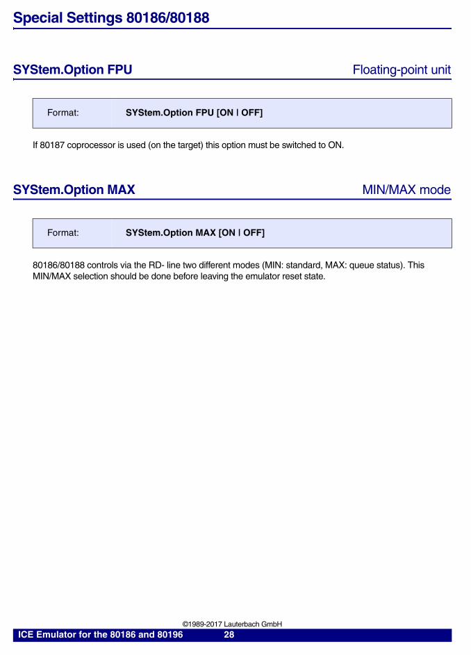
Special Settings 80186/80188
SYStem.Option FPU Floating-point unit
If 80187 coprocessor is used (on the target) this option must be switched to ON.
SYStem.Option MAX MIN/MAX mode
80186/80188 controls via the RD- line two different modes (MIN: standard, MAX: queue status). This MIN/MAX selection should be done before leaving the emulator reset state.
Format: SYStem.Option FPU [ON | OFF]
Format: SYStem.Option MAX [ON | OFF]
ICE Emulator for the 80186 and 80196 28 ©1989-2017 Lauterbach GmbH

Special Settings C186(XL)/C188(XL)/EA and Restrictions
Restrictions 80C186(XL)/80C188(XL)/80C186EA/80C188EA
SYStem.Option Enhanced Enhanced mode
If running in target systems the CPU is automatically started in Enhanced mode if the target system uses this mode. In standalone mode this feature must be stimulated by the emulator system.
SYStem.Option FPU Floating-point unit
If 80187 coprocessor is used (on the target) this option must be switched to ON.
Format: SYStem.Option Enhanced [ON | OFF]
RCU The refresh control unit of the 80C186 is disabled, when the emulation is stopped. Refresh of external dynamic memory can be made by the REFresh.StandBy command. The RCU control register should not be modified when the emulation is stopped. The value displayed in memory windows will be wrong.
Format: SYStem.Option FPU [ON | OFF]
ICE Emulator for the 80186 and 80196 29 ©1989-2017 Lauterbach GmbH

Special Settings 80186EB/80188EB/80186EC/80188EC
SYStem.Option FPU Floating-point unit
If 80187 coprocessor is used (on the target) this option must be switched to ON.
Format: SYStem.Option FPU [ON | OFF]
ICE Emulator for the 80186 and 80196 30 ©1989-2017 Lauterbach GmbH
Special Settings 186EM, 188EM and Restrictions
Restrictions 186EM, 188EM
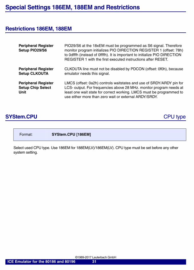
SYStem.CPU CPU type
Select used CPU type. Use 186EM for 188EM(LV)/186EM(LV). CPU type must be set before any other system setting.
Peripheral Register Setup PIO29/S6
PIO29/S6 at the 18xEM must be programmed as S6 signal. Therefore monitor program initializes PIO DIRECTION REGISTER 1 (offset: 78h) to 0dfffh (instead of 0ffffh). It is important to initialize PIO DIRECTION REGISTER 1 with the first executed instructions after RESET.
Peripheral Register Setup CLKOUTA
CLKOUTA line must not be disabled by PDCON (offset: 0f0h), because emulator needs this signal.
Peripheral Register Setup Chip Select Unit
LMCS (offset: 0a2h) controls waitstates and use of SRDY/ARDY pin for LCS- output. For frequencies above 28 MHz. monitor program needs at least one wait state for correct working. LMCS must be programmed to use either more than zero wait or external ARDY/SRDY.
Format: SYStem.CPU [186EM]
ICE Emulator for the 80186 and 80196 31 ©1989-2017 Lauterbach GmbH

SYStem.Line ADDR Shared address pins
18xEM have shared A17-A19/PIO7-PIO9 pins. If pins should be used as address lines, the configuration must be set by the SYStem.LINE ADDR command. Each set bit indicates that the address line should be used.
SYStem.Line SRDY SRDY pin
18xEM have a shared SRDY/PIO6 pin. It is necessary to switch SYStem.Line SRDY to on, if function SRDY is used. If PIO6 is used, SYStem.Line SRDY must be switched off.
Format: SYStem.Line ADDR <mask>
Format: SYStem.Line SRDY [ON | OFF]
ICE Emulator for the 80186 and 80196 32 ©1989-2017 Lauterbach GmbH

Special Settings 186ES, 188ES, 186ED and Restrictions
Restrictions 186ES, 188ES, 186ED
SYStem.CPU CPU type
Select used CPU type. Use 186ES for 188ES(LV)/186ES(LV) or 186ED for 186ED(LV). CPU type must be set before any other system setting.
Peripheral Register Setup PIO29/S6
PIO29/S6 at the 18xES/186ED must be programmed as S6 signal. Therefore monitor program initializes PIO DIRECTION REGISTER 1 (offset: 78h) to 0dfffh (instead of 0ffffh). It is important to initialize PIO DIRECTION REGISTER 1 with the first executed instructions after RESET.
Peripheral Register Setup Watchdog
The watchdog timer at the 18xES/186ED is disabled from monitor program via WDTCON (offset: 0e6h).
Peripheral Register Setup CLKOUTA
CLKOUTA line must not be disabled by PDCON (offset: 0f0h), because emulator needs this signal.
Peripheral Register Setup Chip Select Unit
LMCS (offset: 0a2h) controls waitstates and use of SRDY/ARDY pin for LCS- output. For frequencies above 28 MHz. monitor program needs at least one wait state for correct working. LMCS must be programmed to use either more than zero wait or external ARDY/SRDY.
Peripheral Register Setup Chip Select Unit and AUXCON bus width Control
The bus width of LMCS (offset: 0a2h) must be set to 16bit. This is done in AUXCON register (offset: 0f2h). The reason for this restriction is the internal running monitor program of the emulator, which must run under 16bit bus width.
Format: SYStem.CPU [186ES | 186ED]
ICE Emulator for the 80186 and 80196 33 ©1989-2017 Lauterbach GmbH

SYStem.Line ADDR Shared address pins
18xES/186ED have shared A17-A19/PIO7-PIO9 pins. If pins should be used as address lines, the configuration must be set by the SYStem.LINE ADDR command. Each set bit indicates that the address line should be used.
SYStem.Line SRDY SRDY pin
18xES/186ED have a shared SRDY/PIO6 pin. It is necessary to switch SYStem.Line SRDY to on, if function SRDY is used. If PIO6 is used, SYStem.Line SRDY must be switched off.
Mapping
For basic function of mapper please refer to Emulator User’s Guide.
Format: SYStem.Line ADDR <mask>
Format: SYStem.Line SRDY [ON | OFF]
ICE Emulator for the 80186 and 80196 34 ©1989-2017 Lauterbach GmbH

MAP.BUS8 Bus width mapping
18x/186ED have a chip select dependent bus width control. This control is implemented in AUXCON
register (Offset: F2h). If any of the chip select units is used in 8bit mode, MAP.BUS8 must be set for the corresponding range. 16bit bus width is the default selection
The MAP.RESet command sets the bus width definition to 16 bit.
Format: MAP.BUS8 <range>
Format: MAP.NOBUS8 [<range>]
map.bus8 d:0x040000++0xffff ; MSIZ=1
map.nobus8 ; remaps all to 16 bit
NOTE: The bus width of LMCS (offset: 0a2h) must be set to 16bit. This is done in AUXCON register (offset: 0f2h). The reason for this restriction is the internal running monitor program of the emulator, which must run under 16bit bus width.
ICE Emulator for the 80186 and 80196 35 ©1989-2017 Lauterbach GmbH

Special Settings 186ER/188ER and Restrictions
Restrictions 186ER/188ER
SYStem.CPU CPU type
Select used CPU type. Use 186ER for 188ER or 186ER. CPU type must be set before any other system setting.
SYStem.Line ADDR Shared address pins
18xER has shared A17-A19/PIO7-PIO9 pins. If pins should be used as address lines, the configuration must be set by the SYStem.LINE ADDR command. Each set bit indicates that the address line should be used.
Peripheral Register Setup PIO29/S6
PIO29/S6 at the 18xER must be programmed as S6 signal. Therefore monitor program initializes PIO DIRECTION REGISTER 1 (offset: 78h) to 0dfffh (instead of 0ffffh). It is important to initialize PIO DIRECTION REGISTER 1 with the first executed instructions after RESET.
Peripheral Register Setup CLKOUTA
CLKOUTA line must not be disabled by PDCON (offset: 0f0h), because emulator needs this signal.
Peripheral Register Setup Chip Select Unit
LMCS (offset: 0a2h) controls waitstates and use of SRDY/ARDY pin for LCS- output. For frequencies above 28 MHz. monitor program needs at least one wait state for correct working. LMCS must be programmed to use either more than zero wait or external ARDY/SRDY.
Internal RAM (Onchip)
The 18xER internal RAM must not be used at base address 0 (lowest 32 KByte). All other addresses are allowed. See also SYStem.Option IMDIS and SYStem.Option SREN.
Format: SYStem.CPU [186ER]
Format: SYStem.Line ADDR <mask>
ICE Emulator for the 80186 and 80196 36 ©1989-2017 Lauterbach GmbH

SYStem.Line SRDY SRDY pin
18xER has a shared SRDY/PIO6 pin. It is necessary to switch SYStem.Line SRDY to on, if function SRDY is used. If PIO6 is used, SYStem.Line SRDY must be switched off.
SYStem.Option CLKSEL Clock select
Use this option to select clocking mode. CPU input clock is multiplied by four (default), multiplied by one or divided by two. If divide by two mode is selected, the PLL is disabled.
SYStem.Option IMDIS Internal memory disable
Use this option to disable the 18xER onchip RAM (32 kByte). When this option is switched to ON, onchip memory is always hidden, also if IMCS register bit 9 (internal RAM enable) is set. If option is switched to OFF, onchip memory is available if IMCS register bit 9 is set. Onchip memory can be used, but not at base address 0 (lowest 32 kByte). For analyzer trace to onchip memory see under SYStem.Option SREN.
SYStem.Option SREN Show read enable
Use this option to show read data on the 18xER onchip RAM accesses. Note that if a byte read is being shown, the unused byte will also be driven on the AD15-AD0 bus.
When this option is switched to ON, read data on onchip memory accesses are always visible, also if IMCS register bit 10 (show read) is reset. If option is switched to OFF, read data on onchip memory accesses are available, if IMCS register bit 10 is set. Onchip memory can be used, but not at base address 0 (lowest 32 kByte).
Format: SYStem.Line SRDY [ON | OFF]
Format: SYStem.Option CLKSEL [<*4 | *1 | /2>]
Format: SYStem.Option IMDIS [ON | OFF]
Format: SYStem.Option SREN [ON | OFF]
ICE Emulator for the 80186 and 80196 37 ©1989-2017 Lauterbach GmbH

Special Settings 186CC/CU/CH and Restrictions
Restrictions 186CC/CU/CH
SYStem.Line SRDY SRDY pin
186CC/CU/CH has a shared SRDY/PIO35 pin. It is necessary to switch SYStem.Line SRDY to ON, if function SRDY is used. If PIO35 is used, SYStem.Line SRDY must be switched OFF. In this mode a 10kOhm pull-down resistor is active. A 100kOhm pull-down resistor is always active.
Peripheral Register Setup BHE-/PIO34/ADEN-
BHE-/PIO34 must be programmed as BHE- signal. ADEN- is held low on power-on reset by the emulator. Therefore the AD bus drives both addresses and data, regardless of how software configures the DA bit setting.
Peripheral Register Setup Watchdog
The watchdog timer is disabled from monitor program via WDTCON (offset: 3e0h).
Peripheral Register Setup CLKOUTA
CLKOUTA line must not be disabled by SYSCON (offset: 3f0h), because emulator needs this signal.
Peripheral Register Setup Chip Select Unit
LMCS (offset: 3a2h) controls waitstates and use of SRDY/ARDY pin for LCS- output. For frequencies above 28 MHz. monitor program needs at least one wait state for correct working. LMCS must be programmed to use either more than zero wait or external ARDY/SRDY. If DRAM is used for LCS (LDEN=1) ARDY/SRDY pin is ignored. Therefore one internal wait should be programmed in the LMCS register.
Peripheral Register Setup Chip Select Unit and AUXCON Bus width Control
The bus width of LMCS (offset: 3a2h) must be set to 16bit. The reason for this restriction is the internal running monitor program of the emulator, which must run under 16bit bus width.
Format: SYStem.Line SRDY [ON | OFF]
ICE Emulator for the 80186 and 80196 38 ©1989-2017 Lauterbach GmbH

SYStem.Line ARDY ARDY pin
186CC/CU/CH has a shared ARDY/PIO8 pin. It is necessary to switch SYStem.Line ARDY to ON, if function ARDY is used. If PIO8 is used, SYStem.Line ARDY must be switched OFF. In this mode a 10kOhm pull-down resistor is active. A 100kOhm pull-down resistor is always active.
SYStem.Option CLKSEL Clock select
Use this option to select clocking mode. CPU Input clock is multiplied by two (default), by four or by one or used without PLL (bypass). The data sheet should be checked for the allowed frequency ranges.
Format: SYStem.Line ARDY [ON | OFF]
Format: SYStem.Option CLKSEL [<*2 | *4 | *1/BYPASS>]
ICE Emulator for the 80186 and 80196 39 ©1989-2017 Lauterbach GmbH

Special Settings V40/V50 and Restrictions
Restrictions V40/V50
Waitstates For memory accesses, not more than 7 waitstates should be used. Using more waitstates inhibits emulator to break correctly.
ICE Emulator for the 80186 and 80196 40 ©1989-2017 Lauterbach GmbH

Exception Control
The exception control system depends on the processor used. The window shown here is for the 80(C)186/XL/EA. The exception control system can only control external interrupt sources (see also General Restrictions)
Format: eXception.Enable ON
Format: eXception.Enable OFF
Format: eXception.Activate OFF
Format: eXception.Enable OFF
Enable ON Enable all exception lines.
Enable OFF Disable all exception lines.
Activate OFF Inactivate all exception lines.
Pulse OFF Disable all pulse exceptions.
E::w.xexception Activate Enable Trigger Puls Puls
OFF OFF OFF OFF OFF Single ON RESIN ON ON RESIN Width
RESet HOLD RESIN RESIN INT0 1.000us HOLD RESET HOLD PERiod NMI HOLD NMI 0.000 INT0 HLDA EINT0+ INT1 PULS EINT0- Vector INT2 VINT0+ 00 (000.) INT3 VINT0- TMRIN0 TMRIN1 DRQ0 DRQ1
ICE Emulator for the 80186 and 80196 41 ©1989-2017 Lauterbach GmbH

Reset
Reset Input (not 8086/8088/V20/V30)
Format: eXception.Enable RESIN [ON | OFF]
Format: eXception.Activate RESIN [ON | OFF]
Enable RESIN Enables the RESIN line.
Activate RESIN
Activates the RESIN line.
+1 > Trace / X.TriggerVCC
22k
RES- >X.Enable- >=1 X.Activate- & > RES- (CPU)Run- X.Puls-
Sys.Reset
ICE Emulator for the 80186 and 80196 42 ©1989-2017 Lauterbach GmbH

Reset Input (8086/8088/V20/V30)
NMI
Format: eXception.Enable RESET [ON | OFF]
Format: eXception.Activate RESET [ON | OFF]
Enable RESET Enables the RESET line.
Activate RESET
Activates the RESET line.
Format: eXception.Enable NMI [ON | OFF]
Enable NMI Enables the NMI line.
+1 > Trace / X.TriggerGND
22k
RESET >X.Enable & X.Activate >=1 > RESET (CPU)Run X.Puls
SYS.RESO
+1 > TraceGND
22k
NMI >X.Enable & X.Activate >=1 > NMI (CPU)Run X.Puls
Break
ICE Emulator for the 80186 and 80196 43 ©1989-2017 Lauterbach GmbH

HOLD
DMA Modes
External DMA circuits request the bus by the HOLD signal. If realtime emulation is stopped external and internal DMA circuits will not get access to the bus. They are requesting the bus, but no HLDA signal is generated. If external DMA should be enabled at every time, the HOLD line will always have to be enabled. Internal DMA functions are simultaneously stopped when emulation stop (Break by NMI).
While emulation is stopped, the DMA function will be interrupted for about 10 cycles if the CPU executes internal monitor functions. This may force malfunction, if the DMA needs very fast memory access response times.
SYStem.Line HOLD Enable HOLD line (emulation stopped)
This option allows DMA access without running realtime emulation. If external DMA should be enabled at every time, the HOLD line must always be enabled (SYStem.Line HOLD ON). External DMA circuits are not stopped on breakpoints.
Format: eXception.Enable HOLD [ON | OFF]
Format: eXception.Activate HOLD [ON | OFF]
Enable HOLD Enables the HOLD line.
Activate HOLD
Activates the HOLD line.
Format: System.Line HOLD [ON | OFF]
+1 > Trace / X.TriggerGND
22k
HOLD >X.Enable & X.Activate >=1 > HOLD (CPU)Run X.Puls
Dualport
ICE Emulator for the 80186 and 80196 44 ©1989-2017 Lauterbach GmbH

Interrupt and Timer Control
As interrupt signals or timer signals are bidirectional, the control is done by analog switches.
Format: Exception.Enable <option> [ON | OFF]
<option>: INTR (8086/8088/V20/V30)INT0 .. INT3 ((C)186(XL)/(C)188(XL)/80C186EA/80C188EA)INT0 .. INT4 (80186EB/80188EB)INT0 .. INT7 (80186EC/80188EC)INTP1 .. INTP7 (V40/V50)TMRIN0 ((C)186(XL)/(C)188(XL)/EA/EB/EC/EM/ES/ER/ED/CC)TMRIN1 ((C)186(XL)/(C)188(XL)/EA/EB/EC/EM/ES/ER/ED/CC)DRQ0 .. DRQ1 ((C)186(XL)/(C)188(XL)/EA/EM/ES/ER/ED/CC)DRQ0 .. DRQ3 (V40/V50/80186EC/80188EC)
+1 > Trace
Target <> S1 <> CPU
22k 22k
GND GND S1 = 50 (HC4066)
ICE Emulator for the 80186 and 80196 45 ©1989-2017 Lauterbach GmbH

DRQ0 Enables the DRQ0 line.
DRQ1 Enables the DRQ1 line.
DRQ2 Enables the DRQ2 line.
DRQ3 Enables the DRQ3 line.
INT0 Enables the INT0 line.
INT1 Enables the INT1 line.
INT2 Enables the INT2 line.
INT3 Enables the INT3 line.
INT4 Enables the INT4 line.
INT5 Enables the INT5 line.
INT6 Enables the INT6 line.
INT7 Enables the INT7 line.
INTP1 Enables the INTP1 line.
INTP2 Enables the INTP2 line.
INTP3 Enables the INTP3 line.
INTP4 Enables the INTP4 line.
INTP5 Enables the INTP5 line.
INTP6 Enables the INTP6 line.
INTP7 Enables the INTP7 line.
INTR Enables the INTR line.
TMRIN0 Enables the TMRIN0 line.
TMRIN1 Enables the TMRIN0 line.
ON Enables all exception line.
OFF Disables all exception lines.
ICE Emulator for the 80186 and 80196 46 ©1989-2017 Lauterbach GmbH

Interrupt Stimulation
Interrupt stimulation is only possible in Stand-Alone mode or if no external interrupt controller is used. The simulation circuit supports level and edge triggered interrupts with and without external vector support.
The possible interrupt line depend on the CPU used. The following description is for the 80186/XL/EA processors. The functionality is the same for other processors.
Format: Exception.Puls <option> <time> <period>
<option>: INT0EINT0+EINT0-VINT0+VINT0-
EINT0- Stimulate EINT0- line.
HOLD Stimulate HOLD line.
INT0 Stimulate INT0 line.
INTR Stimulate INTR line.
NMI Stimulate NMI line.
RESET Stimulate RESET line.
RESIN Stimulate RESIN line.
VINT0- Stimulate VINT0- line.
OFF No stimulation on any exception line.
+1 > TraceGND
22k
INTx >X.Enable INTx & >=1 > INTx (CPU)
X.Puls
ICE Emulator for the 80186 and 80196 47 ©1989-2017 Lauterbach GmbH

INT0
This is the simulation for vectored interrupts in cascaded mode. The simulation circuit sets INT0 to high until 2 interrupt acknowledge cycles are executed. The vector is supplied on the second IACK cycle. The pulse width should be at minimum 2 CPU cycles.
E::w.xException setup Trigger Puls Puls
OFF OFF SingleON RESIN Width
RESIN INT0 10.000usRESET HOLD PERiodHOLD NMI 0.000HLDA EINT0+PULS EINT0- Vector
VINT0+ 33 (051.)VINT0-
E::w.a.l ,t.0 def Analyzer listrun address cycle d.w sy
AP:000000401 fetch 00AP:000000402 fetch 04AP:000000403 fetch 00 Stimulation pulsAP:000000404 fetch 00
jmp 0000:0400AP:000000405 fetch 00AD:000000400 iack 00 1st IACK cycleAD:000000400 iack 33 2nd IACK cycle, vectorAD:0000000CC rd-mem 00AD:0000000CD rd-mem 05 vector table readAD:0000000CE rd-mem 00AD:0000000CF rd-mem 00AD:000000FF2 wr-mem 02AD:000000FF3 wr-mem F2 stack writeAD:000000FF0 wr-mem 00AD:000000FF1 wr-mem 00AD:000000FEE wr-mem 00AD:000000FEF wr-mem 04AP:000000500 fetch EA interrupt programAP:000000501 fetch 00
ICE Emulator for the 80186 and 80196 48 ©1989-2017 Lauterbach GmbH

EINT0+ The pulse generator is directly connected to the interrupt pin. A low to high pulse is generated. No interrupt vector is supplied by the simulation logic (Fully nested mode).
EINT0- The pulse generator is directly connected to the interrupt pin. A high to low pulse is generated. No interrupt vector is supplied by the simulation logic (Fully nested mode).
VINT0+ The pulse generator is directly connected to the interrupt pin. A low to high pulse is generated. All IACK cycles are supplied with the interrupt vector defined by the eXception.Vector field.
VINT0- The pulse generator is directly connected to the interrupt pin. A high to low pulse is generated. All IACK cycles are supplied with the interrupt vector defined by the eXception.Vector field.
ICE Emulator for the 80186 and 80196 49 ©1989-2017 Lauterbach GmbH

Trap Trigger
Every trap can be used as a separate trigger point. Trap trigger is detected by accessing the vector table!
Format: eXception.Trigger <vector>
<vector>: 0. … 255.
HLDA Trigger on HLDA line.
HOLD Trigger on HOLD line.
Pulse Trigger on Pulse line.
RESET Trigger on RESET line.
RESIN Trigger on RESIN line.
ON Trigger on all exception lines.
OFF No trigger on any exception lines.
x.t 2 on ; activate NMI trigger
x.t 2 off ; deactivate NMI trigger
x.t 0x0--0x0ff off ; switch off all vector triggers
x.t 0x80--0x0ff ; set vectors 128 to 255 trigger active
ICE Emulator for the 80186 and 80196 50 ©1989-2017 Lauterbach GmbH

Refresh Operation
The probe supports refresh operation in realtime emulation, but the refresh function is stopped when emulation stops and starts again on realtime emulation. The CDRAM register value must be 40H (80H C188) at minimum! When emulation is stopped, the REFresh system of the emulator has to generate valid refresh cycles for the target system. Refresh doesn't work together with the Request access mode. Use Denied or Nodelay access mode in this case.
FPU
FPU commands
Format: FPU.ON
Format: FPU.OFF
Format: FPU.RESet
Format: FPU.view
Format: FPU.Set <register> <value>
ON/OFF FPU display option is switched on or off
RESet FPU is initialized via 'finit' instruction
view Display window. The display is only updated, if the FPU is in idle state
FPU.Set Changes FPU registers
E::w.fpuIM I IE _ C0 _ CW 037F ST(0) 1.2 3FFF.999999999999DM D DE _ C1 _ SW 3000 ST(1) 3.4 4000.D99999999999ZM Z ZE _ C2 _ TW 0FFF ST(2) NAN FFFF.C00000000000OM O OE _ C3 _ TOP 6 ST(3) NAN FFFF.C00000000000UM U UE _ B _ ST(4) NAN FFFF.C00000000000PM P PE _ OPC 0106 ST(5) NAN FFFF.C00000000000PC S SF _ IP 00000B00 ST(6) NAN FFFF.C00000000000RC C ES _ OP 00010280 ST(7) NAN FFFF.C00000000000
ICE Emulator for the 80186 and 80196 51 ©1989-2017 Lauterbach GmbH

I/O Connector for Coprocessor (8086/8087)
Signals connected through 8087 on the 8086 emulator pod. For a description look under SYStem.Option FPU.
9 7 5 3 110 8 6 4 2
1 CLK 2 GND3 RQ/GT0- 4 GND5 RQ/GT1- 6 GND7 INT 8 GND9 BUSY 10 GND
ICE Emulator for the 80186 and 80196 52 ©1989-2017 Lauterbach GmbH

Memory Classes
Access Class Description
D Data
P Program
IO IO
ED Dualport Data
EP Dualport Program
EIO Dualport I/O
A Absolute
AD Absolute Data
AP Absolute Program
AC Absolute CPU
EA Absolute Dualport
EAD Absolute Dualport Data
EAP Absolute Dualport Program
EAC Absolute Dualport CPU
ICE Emulator for the 80186 and 80196 53 ©1989-2017 Lauterbach GmbH

C:, P: and D: This access types use all the same memory by default. Using System.Option SPLIT it is possible to use separate emulation memory for program and data accesses. If no segment address is used, the D: prefix will refer to DS and the P: prefix to CS register
d.s P:0--0ffff 0d.s 0--0ffff 0d.s 100 0
; fill program memory with zero; fill data memory with zero; set location ds:100 to 0
d.a 100 nopd.a 0--0fff nop
; assemble to location cs:100; fill program memory with nop; instruction
d.i AD:1000 ; read memory mapped i/o from; physically address 1000h
d.a 40:0 nop ; writes NOP to address 40:0 (400H)
IO:, AIO:, EIO:, EAIO:
The I/O addressing is always absolute. The IO-Range is 64K. Upper address bits are cut.
d.s IO:0x100 0x33 0x44 ; write 33H to port 100H and 44H to 101H
d.o 0x100 'A' ; sets port
d.i 0x100 ; read one byte from port 100H
d IO:0x100--0x103 ; displays 4 ports from 100H to 103H
d EIO:0x100--0x103 ; display state of output ports via; dualport memory
A:, EA: Absolute addressing. The address parameter specifies the physically address.
d.s A:0x12000 0x33 ; write to address 12000H in program/data; memory
d EA:0x12000 ; displays absolute address 12000H from; dualport memory
ICE Emulator for the 80186 and 80196 54 ©1989-2017 Lauterbach GmbH
Segmentation
The MMU setup is normally done by loading a program. The section-table of the object-file (segments, groups) is used to define the valid physical areas for the translation of physical addresses to logical addresses. For more detailed information see command MMU.
Segment and offset are separated by a colon. If no segment is defined, the emulator will use the CS: segment for program related commands and the DS: segment for data related commands. The D: access class will force the usage of the DS: segment and the P: access class will force usage of the CS: segment.
Segment Description
CS: Current value of CS
DS: Current value of DS
SS: Current value of SS
ES: Current value of ES
<number>: Any hex segment number
<seg_name>: Any segment name for the sYmbol.SECtion table
d.s DS:0x100 ; if DS register is 10H, the physical; address is DS*10H+addr = 200H
d.a 0x200 ; assemble to CS:200
d.s 0x100 0x0 ; set location DS:100
d SS:0x0f000 ; displays stack segment
d.l 0x0ffff:0x0 ; list code is segment 0ffff
d far_romdata:0x0 ; dump segment 'far_romdata'
ICE Emulator for the 80186 and 80196 55 ©1989-2017 Lauterbach GmbH

Banked Target Systems
Banking as described in this chapter refers to address extension of 80x86 processors, not the internal segmentation of the 80x86 family. In banked systems the upper address lines are supplied by the external bank probe. Four additional lines offer 16 different memory banks. Accessing the different pages is done by adding an extra bank component to all logical addresses and extending all physical memory addresses to 24 bit. The physical address bits A20 to A23 select the memory bank. Every command which makes a memory access first calls a special bank driver subroutine to select the temporary memory bank. On realtime emulation the bank number is traced on the upper four bits of the address bus. On a breakpoint the upper four bit of the address bus are stored to the bank number of the PP register (Program Pointer).
This command loads the bank driver. The bank driver is a special subroutine to select the actual bank. Loading a special bank driver gives a maximum of flexibility to the user. A bank address delivered by the emulator may be used to set microcontroller ports or external MMUs in the target system. The bank file consists of a code number defining the bank operation mode and a code area which consists of a subroutine to set the correct bank state. The internal bank number is placed in register AL when calling the subroutine. The reason for the call is placed in AH. It can be initialization (0), read (1), write (2), or start execution (3). Writes to internal CPU ports may be executed directly, while ports in target systems must be accessed by a special system call (see end of this chapter). The internal bank address is placed in accu A when calling the subroutine. The PP (Program Pointer) register hold the logical 24-bit PC address. The translation between logical bank and physical bank (also for the common areas and I/O space) is done by the MMU command.
On the 80x86 banking can only be done in external mode. External banked systems use a register or output pins of the CPU to generate the upper memory addresses. These lines must be feedback to the emulator with the bank probe (lines 0 to 3). Unused inputs of the bank probe must be grounded (or jumpered to ground pin).
Format: SYStem.BankFile <file>
Format: SYStem.Bank <option>
<option>: OFFEXTernal
; This example uses a common program/data area on a:0x0--0x0bffffh;a banked area from a:0x0c0000--0x0fffff with 16 banks
map.res ; reset mapper
map.mirror ap:0--0bffff ap:100000map.mirror ap:0--0bffff ap:200000...map.mirror ap:0--0bffff ap:0e00000map.mirror ap:0--0bffff ap:0f00000
; mirror for common area
ICE Emulator for the 80186 and 80196 56 ©1989-2017 Lauterbach GmbH

This example selects the bank by writing the left shifted bank to io:204:
map.mirror aio:0--ffff aio:100000map.mirror aio:0--ffff aio:200000...map.mirror aio:0--ffff aio:0e00000map.mirror aio:0--ffff aio:0f00000
; mirror I/O area (not banked)
map.ram ap:0c0000--0fffffmap.ram ap:1c0000--1fffff...map.intern
; map bank #0; map bank #1
symbol.resetsystem.bankfile banksel.bnksystem.up
; clear old symbols first; load bank file
d.load.o bank0.omf 0:0:0 /mfd.load.o bank1.omf 1:0:0 /mf /ncd.load.o bank2.omf 2:0:0 /mf /nc...d.load.o bank14.omf 0e:0:0 /mf /ncd.load.o bank15.omf 0f:0:0 /nc
org 0:3effH ; pseudo org (use inline assembler)
db 0x2 ; select external mode
bank: ; AL is bank address, AH is reason
org 0:3f00H ; destination area in system memory
shl al,1mov dx,204Hcall 0d30H
ret
; set DX to io register; subroutine to write byte to i/o; DX is address, AL is data; return
ICE Emulator for the 80186 and 80196 57 ©1989-2017 Lauterbach GmbH

Memory and I/O Access Routines
The following routines are available in the emulation control monitor to access external memory or i/o:
Addr Function Address Data Result
0d00H ReadMemByte ES:SI - AL
0d04H ReadMemWord ES:SI - AX
0d10H WriteMemByte ES:DI AL -
0d14H WriteMemWord ES:DI AX -
0d20H ReadIOByte DX - AL
0d24H ReadIOWord DX - AX
0d30H WriteIOByte DX AL -
0d34H WriteIOWord DX AX -
ICE Emulator for the 80186 and 80196 58 ©1989-2017 Lauterbach GmbH

Monitor Extensions
A monitor extension is a piece of code that’s extending the emulation control monitor. The emulation monitor is responsible for starting and stopping the target program and accessing memory and registers when the target program is stopped. This monitor is running in a hidden memory inside the ECU unit. Extensions must be made available in a binary program. This program must be loaded before activating the emulation by the following command:
The program can contain the following extensions:
For more details about the definition of the monitor extension and parameter passing see the example file './demo/i86/etc/monext.asm'.
Format: SYStem.MonFile <file>
Start Target This part is executed before the target program is started. It can enable timers in the target or reset watchdogs.
Stop Target This part is executed after the emulation in the target has stopped. It can disable timers or external watchdogs.
Read Memory User specific memory read. Allows access to special memories, e.g. serial connected EEPROMs. The access is made by the USR: memory class.
Write Memory User specific memory write. Allows write access to special memories, e.g. programming EEPROM or FLASH memories. The access is made by the USR: memory access class.
ICE Emulator for the 80186 and 80196 59 ©1989-2017 Lauterbach GmbH

State Analyzer
When the bus size of the processor is changed, an existing analyzer recording, sampled with a different bus size, will be displayed wrong.
Keywords for the Trigger Unit
General Keywords for the Trigger Unit
Input Event Meaning Analyzer Hardware
ECC8 HAC HA120 SA120
BYTE Byte transfer X X
PORT Input line from port analyzer X X
Wait0..Wait6 Waitstates 0..6 X X
WaitX Waitstates greater 6 X X
WORD Word transfer X X
ICE Emulator for the 80186 and 80196 60 ©1989-2017 Lauterbach GmbH

8086/8088/V20/V30MAX Keywords for the Trigger Unit
Input Event Meaning Analyzer Hardware
ECC8 HAC HA120 SA120
Data Data access (MRD or MWR) X X X
FETCH Program fetch cycle X X X
IE Interrupt enable bit X X
INTA INTA line X X X
INTR Interrupt request X X
IO IO cycle (IORD or IOWR) X X X
IORD IO read access cycle X X X
IOWR IO write access cycle X X X
LOCK Lock signal X X
MRD Memory read access cycle X X X
MWR Memory write access cycle X X X
Read Read access (FETCH or INTA or IORD or MRD)
X X X
STACK Stack access X X
TEST Test line X X
Write Write access (IOWR or MWR) X X X
ICE Emulator for the 80186 and 80196 61 ©1989-2017 Lauterbach GmbH

8086/8088/V20/V30MIN Keywords for the Trigger Unit
80(C)186(XL)/80(C)188(XL)/EA/EB/EC/EM/ES/ER Keywords for the Trigger Unit
Input Event Meaning Analyzer Hardware
ECC8 HAC HA120 SA120
Data Data access (MRD or MWR) X X X
FETCH Program fetch cycle X X
IE Interrupt enable bit X X
INTR Interrupt request X X
IO IO cycle (IORD or IOWR) X X X
IORD IO read access cycle X X X
IOWR IO write access cycle X X X
MRD Memory read access cycle X X X
MWR Memory write access cycle X X X
Read Read access (IORD or MRD) X X X
STACK Stack access X X
TEST Test line X X
WR Write line X X
Write Write access (IOWR or MWR) X X X
ICE Emulator for the 80186 and 80196 62 ©1989-2017 Lauterbach GmbH

Input Event Meaning Analyzer Hardware
ECC8 HAC HA120 SA120
Data Data access (MRD or MRDDMA or MWR or MWRDMA)
X X X
DMA DMA cycle (IORDDMA or IOWRDMA or MRDDMA or MWRDMA)
X X X
FETCH Program fetch cycle X X X
HALT Halt cycle X X X
IACK Interrupt acknowledge X X X
INT Interrupt request (INT0 or INT1 or INT2 or INT3)
X X
INT0..INT3 X X
IO IO cycle (IORD or IORDDMA or IOWR or IOWRDMA)
X X X
IORD IO read access cycle X X X
IORDDMA IO read access cycle by DMA X X X
IOWR IO write access cycle X X X
IOWRDMA IO write access cycle by DMA X X X
MRD Memory read access cycle X X X
MRDDMA Memory read access cycle by DMA X X X
MWR Memory write access cycle X X X
MWRDMA Memory write access cycle by DMA X X X
Read Read access (FETCH or IACK or IORD or IORDDMA or MRD or MRDDMA)
X X X
REFRESH X X
TEST Test line X X
Write Write access (IOWR or IOWRDMA or MWR or MWRDMA)
X X X
ICE Emulator for the 80186 and 80196 63 ©1989-2017 Lauterbach GmbH

V40/V50 Keywords for the Trigger Unit
For not CPU-specific keywords, see non-declarable input variables in “ICE/FIRE Analyzer Trigger Unit Programming Guide” (analyzer_prog.pdf).
Input Event Meaning Analyzer Hardware
ECC8 HAC HA120 SA120
Data Data access (MRD or MRDDMA or MWR or MWRDMA)
X X X
DMA DMA cycle (IORDDMA or IOWRDMA or MRDDMA or MWRDMA)
X X X
FETCH Program fetch cycle X X X
HALT Halt cycle X X X
IACK Interrupt acknowledge X X X
INT Interrupt request (INTP1 or INTP2 or INTP3)
X X
INTAK INTAK line X X
INTP1..INTP3 X X
IO IO cycle (IORD or IORDDMA or IOWR or IOWRDMA)
X X X
IORD IO read access cycle X X X
IORDDMA IO read access cycle by DMA X X X
IOWR IO write access cycle X X X
IOWRDMA IO write access cycle by DMA X X X
MRD Memory read access cycle X X X
MRDDMA Memory read access cycle by DMA X X X
MWR Memory write access cycle X X X
MWRDMA Memory write access cycle by DMA X X X
POLL Poll line X X
Read Read access (FETCH or IACK or IORD or IORDDMA or MRD or MRDDMA)
X X X
REFRESH X X
Write Write access (IOWR or IOWRDMA or MWR or MWRDMA)
X X X
ICE Emulator for the 80186 and 80196 64 ©1989-2017 Lauterbach GmbH

Keywords for the Display
General Keywords
8086/8088/V20/V30MAX Keywords
8086/8088/V20/V30MIN Keywords
80(C)186(XL)/80(C)188(XL)/EA/EB/EC/EM/ES/ER/ED/CC Keywords
AAddress Absolute (physical) address
Wait Number of inserted wait cycles, for more than 6 a 'X' appears.
RESET Reset cycle
QS0, QS1 Queue state lines
NMI NMI line
RQGT0, RQGT1 CPU lines
IE Interrupt enable bit
INTR Interrupt line
LOCK LOCK line
TEST TEST line
INTA INTA line
HOLD, HLDA CPU lines
IE Interrupt enable bit
INTR Interrupt line
WR WR line
TEST TEST line
DMA DMA access
RESIN RESIN line
RESET Reset cycle
TMRIN0, TMRIN1 Timer inputs
NMI NMI line
ICE Emulator for the 80186 and 80196 65 ©1989-2017 Lauterbach GmbH
V40/V50MIN Keywords
Dequeueing
The disassembled lines in the analyzer are displayed prior to the resulting data cycles. This dequeueing fails for commands which have not a constant number of data cycles. Long data sequences during REP SCAS or REP MOVS can cause missing mnemonics in the disassembly.
HOLD, HLDA CPU lines
INT0 .. INT3 Interrupt lines
TEST TEST line
RESIN RESIN line
RESET Reset cycle
TCLK,TCTL2,TOUT2 Timer lines
NMI NMI line
HOLD, HLDA CPU lines
INTP1 .. INTP3 Interrupt lines
POLL POLL line
INTAK Interrupt line
ICE Emulator for the 80186 and 80196 66 ©1989-2017 Lauterbach GmbH
Port Analyzer
Keywords for the Port Analyzer (8086/8088/V20/V30)
INTA INTA line (MIN)
ALE ALE (MIN)
HOLD HOLD (MIN)
HLDA HLDA (MIN)
RESET RESET output (MAX)
INTR Interrupt line (MAX)
NMI NMI (MAX)
QS0, QS1 Queue state (MAX)
RQGT0, RQGT1 RQGTx lines (MAX)
DEN DEN (MIN)
DTR DTR (MIN)
IOM IOM (MIN)
S0 .. S2 State lines (MAX)
RD
WR WR (MIN)
READY READY
BHE BHE
LOCK LOCK (MAX)
CRQGT0, CRQGT1 CRQGTx (MAX)
CINT CINT(MAX)
CBUSY CBUSY (MAX)
TEST TEST (MAX)
A0 .. A7 Free Trace Channels A
B0 .. B7 Free Trace Channels B
C0 .. C7 Free Trace Channels C
BNK0 .. BNK7 Bank Probe Channels
ICE Emulator for the 80186 and 80196 67 ©1989-2017 Lauterbach GmbH

Keywords for the Port Analyzer (80(C)186(XL)/80(C)188(XL)/EA)
RESIN RES input
RESET RESET output
TMRIN0 Timer In 0
TMRIN1 Timer In 1
NMI NMI
ALE ALE
HOLD HOLD
HLDA HLDA
DRQ0 DMA Request 0
DRQ1 DMA Request 1
TMROUT0 Timer Out 0
TMROUT1 Timer Out 1
LCS Lower Chip Select
UCS Upper Chip Select
PCS0 .. 6 Peripheral Chip Selects
MCS0 .. 3 Middle Chip Selects
INT0 .. INT3 Interrupt 0 .. 3
A0 .. A7 Free Trace Channels A
B0 .. B7 Free Trace Channels B
C0 .. C7 Free Trace Channels C
BNK0 .. BNK7 Bank Probe Channels
ICE Emulator for the 80186 and 80196 68 ©1989-2017 Lauterbach GmbH

Keywords for the Port Analyzer (80186EB/80188EB)
RESIN RES input
RESET RESET output
TMRIN0 Timer In 0
TMRIN1 Timer In 1
NMI NMI
ALE ALE
HOLD HOLD
HLDA HLDA
RXD0, TXD0, CTS0 Serial interface
10 .. 17 Port 1
20 .. 27 Port 2
LCS Lower Chip Select
UCS Upper Chip Select
TMROUT0 Timer Out 0
TMROUT1 Timer Out 1
TEST TEST line
NCS NCS line
ERROR ERROR line
PEREQ PEREQ line
INT0 .. INT4 Interrupt 0 .. 3
A0 .. A7 Free Trace Channels A
B0 .. B3 Free Trace Channels B
BNK0 .. BNK7 Bank Probe Channels
ICE Emulator for the 80186 and 80196 69 ©1989-2017 Lauterbach GmbH

Keywords for the Port Analyzer (80186EC/80188EC)
RESIN RES input
RESET RESET output
TMRIN0 Timer In 0
TMRIN1 Timer In 1
NMI NMI
ALE ALE
HOLD HOLD
HLDA HLDA
DRQ0 .. DRQ3 DMA request lines
MCS0,MCS1,MCS3 Chip selects
10 .. 17 Port 1
20 .. 27 Port 2
30 .. 35 Port 3
INTA Interrupt line
WDTOUT WDTOUT line
LCS Lower Chip Select
UCS Upper Chip Select
TMROUT0 Timer Out 0
TMROUT1 Timer Out 1
TEST TEST line
INT0 .. INT7 Interrupt 0 .. 7
BNK0 .. BNK7 Bank Probe Channels
ICE Emulator for the 80186 and 80196 70 ©1989-2017 Lauterbach GmbH

Keywords for the Port Analyzer (18xEM/18xES/18xER/186ED)
18xEM/ER 18xES/ED
RESET RES- input RES- input
TMRIN0 TMRIN0/PIO11 TMRIN0/PIO11
TMRIN1 TMRIN1/PIO0 TMRIN1/PIO0
NMI NMI NMI
ALE ALE ALE
HOLD HOLD HOLD
HLDA HLDA HLDA
INT0 INT0 INT0
IRQ INT3/INTA1/IRQ INT3/INTA1/IRQ
SELECT INT1/SELECT INT1/SELECT
LCS Lower Chip Select Lower Chip Select
UCS Upper Chip Select Upper Chip Select
0 TMRIN1/PIO0 TMRIN1/PIO0
1 TMROUT1/PIO1 TMROUT1/PIO1
2 PCS6/A2/PIO2 PCS6/A2/PIO2
3 PCS5/A1/PIO3 PCS5/A1/PIO3
4 DTR/PIO4 DTR/PIO4
5 DEN/PIO5 DEN/DS/PIO5
6 SRDY/PIO6 SRDY/PIO6
7 A17/PIO7 A17/PIO7
8 A18/PIO8 A18/PIO8
9 A19/PIO9 A19/PIO9
10 TMROUT0/PIO10 TMROUT0/PIO10
11 TMRIN0/PIO11 TMRIN0/PIO11
12 DRQ0/PIO12 DRQ0/INT5/PIO12
13 DRQ1/PIO13 DRQ1/INT6/PIO13
14 MCS0/PIO14 MCS0/PIO14
15 MCS1/PIO15 MCS1/PIO15
16 PCS0/PIO16 PCS0/PIO16
ICE Emulator for the 80186 and 80196 71 ©1989-2017 Lauterbach GmbH

17 PCS1/PIO17 PCS1/PIO17
18 PCS2/PIO18 PCS2/CTS1/ENRX1/PIO18
19 PCS3/PIO19 PCS3/RTS1/RTR1/PIO19
20 SCLK/PIO20 RTS0/RTR0/PIO20
21 SDATA/PIO21 CTS0/ENRX0/PIO21
22 SDEN0/PIO22 TXD0/PIO22
23 SDEN1/PIO23 RXD0/PIO23
24 MCS2/PIO24 MCS2/PIO24
25 MCS3/RFSH/PIO25 MCS3/RFSH/PIO25
26 UZI/PLLBYPS/PIO26 UZI/PLLBYPS/PIO26
27 TXD/PIO27 TXD1/PIO27
28 RXD/PIO28 RXD1/PIO28
29 S6/CLKDIV2/PIO29 S6/LOCK/CLKDIV2/PIO29
30 INT4/PIO30 INT4/PIO30
31 INT2/INTA0/PIO31 INT2/INTA0/PWD/PIO31
A0 .. A7 Free Trace Channels
BNK0 .. BNK7 Bank Probe Channels
ICE Emulator for the 80186 and 80196 72 ©1989-2017 Lauterbach GmbH

Keywords for the Port Analyzer (V40/V50)
RESIN RES input
TCLK,TCTL2,TOUT2 Timer lines
NMI NMI
ALE ALE
HOLD HOLD
HLDA HLDA
INTAK INTAK line
TC TC line
POLL POLL line
REFRQ REFRQ line
DRQ0 .. DRQ3 DMA Request 0 .. 3
DACK0 .. DACK3 DMA Acknowledge 0 .. 3
INTP1 .. INTP7 Interrupt 1 .. 7
A0 .. A7 Free Trace Channels A
B0 .. B7 Free Trace Channels B
C0 .. C7 Free Trace Channels C
BNK0 .. BNK7 Bank Probe Channels
ICE Emulator for the 80186 and 80196 73 ©1989-2017 Lauterbach GmbH

Input Connector for free Channels (8086/8088/80186/80188)
Input Connector for free Channels (80186EB/80188EB)
25 23 21 19 17 15 13 11 9 7 5 3 126 24 22 20 18 16 14 12 10 8 6 4 2
1 A0 17 C02 A1 18 C13 A2 19 C24 A3 20 C35 A4 21 C46 A5 22 C57 A6 23 C68 A7 24 C7
9 B0 25 GND10 B1 26 GND11 B212 B313 B414 B515 B616 B7
15 13 11 9 7 5 3 116 14 12 10 8 6 4 2
1 A0 9 B02 A1 10 B13 A2 11 B24 A3 12 B35 A4 13 GND6 A5 14 GND7 A6 15 GND8 A7 16 GND
ICE Emulator for the 80186 and 80196 74 ©1989-2017 Lauterbach GmbH

Input Connector for free Channels (18xEM/18xES/18xER/186ED/CC)
9 7 5 3 110 8 6 4 2
1 A0 9 GND2 A1 10 GND3 A24 A35 A46 A57 A68 A7
ICE Emulator for the 80186 and 80196 75 ©1989-2017 Lauterbach GmbH

Compilers
Language Compiler Company Option Comment
ASM AXLS HP Source level debugging
C BORLANDC Borland Software Corporation
EOMF-86 with Paradigm LOCATE
C ORGANON CAD-UL ElectronicServices GmbH
EOMF-86 Banking support
C IC86 Intel Corporation OMF-86C MCC86 Mentor Graphics
CorporationEOMF-86 incl. Microtec ext.
C MSC/MSVC-16BIT Microsoft Corporation EOMF-86 with Paradigm LOCATE
C MSC/MSVC Microsoft Corporation EXE/TD with Paradigm LOCATE
C ICC86 TASKING OMF-86C ICC86 TASKING IEEEC++ BORLANDC Borland Software
CorporationEXE/TD
C++ MSVC-16BIT Microsoft Corporation EXE/CVMODULA LOGITECH-M2 Terra Datentechnik MAP/REFPASCAL TEK-PASCAL Tektronix TEKPLM PL/M86 Intel Corporation OMF-86 reads src or list file
ICE Emulator for the 80186 and 80196 76 ©1989-2017 Lauterbach GmbH

3rd Party Tool Integrations
CPU Tool Company Host
WINDOWS CE PLATF. BUILDER
- Windows
CODE::BLOCKS - -C++TEST - WindowsADENEO -X-TOOLS / X32 blue river software GmbH WindowsCODEWRIGHT Borland Software
CorporationWindows
CODE CONFIDENCE TOOLS
Code Confidence Ltd Windows
CODE CONFIDENCE TOOLS
Code Confidence Ltd Linux
EASYCODE EASYCODE GmbH WindowsECLIPSE Eclipse Foundation, Inc WindowsCHRONVIEW Inchron GmbH WindowsLDRA TOOL SUITE LDRA Technology, Inc. WindowsUML DEBUGGER LieberLieber Software
GmbHWindows
SIMULINK The MathWorks Inc. WindowsATTOL TOOLS MicroMax Inc. WindowsVISUAL BASIC INTERFACE
Microsoft Corporation Windows
LABVIEW NATIONAL INSTRUMENTS Corporation
Windows
RAPITIME Rapita Systems Ltd. WindowsRHAPSODY IN MICROC IBM Corp. WindowsRHAPSODY IN C++ IBM Corp. WindowsDA-C RistanCASE WindowsTRACEANALYZER Symtavision GmbH WindowsTA INSPECTOR Timing Architects GmbH WindowsUNDODB Undo Software LinuxVECTORCAST UNIT TESTING
Vector Software Windows
VECTORCAST CODE COVERAGE
Vector Software Windows
ICE Emulator for the 80186 and 80196 77 ©1989-2017 Lauterbach GmbH

Realtime Operation Systems
Company Product Comment
Oracle Corporation ChorusOSMentor Graphics Corporation
Nucleus PLUS
Wind River Systems pSOS+ 2.1 to 2.5, 3.0Quadros Systems Inc. RTXC 3.2Wind River Systems VxWorks 5.x and 6.x
ICE Emulator for the 80186 and 80196 78 ©1989-2017 Lauterbach GmbH

Emulation Frequency
The emulation probe is designed for running with CPU's up to 40 MHz. However the max. speed is limited by the CPU chip used in the emulator. TRACE32 modules are delivered with the fastest CPU available. The following values of emulation frequencies refer to the 'standalone' mode (memory is mapped internal).
The maximum operation frequency of TRACE32-ICE depends on:
• The max. frequency of the CPU
• The access time of the overlay memory (15 ns or 35 ns)
• The mapper mode (Slow or Fast)
• The number of waitstates
(WO = 0 waitstates W1 = 1 waitstate)
Module CPU F-W0-15
F-W0-35
S-W0-15
S-W0-35
S-W1-15
S-W1-35
DRAM
LA-7084 UT80CRH196KDS 16.0+ 16.0+ 16.0+ 15.6 16.0+ 16.0+LA-7097 V20 16.0 14.5 14.8 13.5 16.0+ 16.0+ 16.0LA-7098 V30 16.0 14.5 14.8 13.5 16.0+ 16.0+ 16.0LA-6673 V40 16.0 13.8 14.3 12.5 16.0+ 16.0+ 16.0LA-7095 V50 16.0 13.8 14.3 12.5 16.0+ 16.0+ 16.0
NOTE: The cycle speed of the SA120 unit is limited to 150ns.
ICE Emulator for the 80186 and 80196 79 ©1989-2017 Lauterbach GmbH

Emulation Modules
Module Overview
V40 PLCC68LA-6673
V50 PLCC68LA-7095
V20 DIL40LA-7097
V30 DIL40LA-7098
UT80CRH196KDS PLCC68LA-7084
LA-6670
ICE Emulator for the 80186 and 80196 80 ©1989-2017 Lauterbach GmbH

Order Information
Order No. Code Text
LA-6670 ICE-186 ICE-186 Base ModuleLA-6671 M-80C186XL Module 80C186XLLA-7070 M-80C188XL Module 80C188XLLA-7071 M-80C186EA Module 80C186EALA-7072 M-80C188EA Module 80C188EALA-6672 M-80C186EB Module 80C186EBLA-6697 M-80C186EB-3.3V Module 80C186EB 3.3VLA-7075 M-80C188EB Module 80C188EBLA-6698 M-80C188EB-3.3V Module 80C188EB 3.3VLA-6678 M-80C186EC Module 80C186ECLA-7076 M-80C188EC Module 80C188ECLA-6696 M-80186EM Module 186EMLA-7090 M-80188EM Module 188EMLA-7091 M-80186ES Module 186ESLA-7092 M-80188ES Module 188ESLA-7093 M-80186ER Module 186ERLA-7094 M-80188ER Module 188ERLA-7099 M-80186ED Module 186EDLA-7077 M-80186CC/CU/CH Module 186CC/CU/CHET-1200 ET-80186PLCC-C PLCC to PLCC Clip Over Adapter for 80C186ET-1202 ET-80186/88PLCC-SQFP PLCC to SQFP80 Surface Mountable AdapterLA-6673 M-V40 Module V40LA-7095 M-V50 Module V50LA-6677 M-8086 Module 8086LA-7096 M-8088 Module 8088LA-7097 M-V20 Module V20LA-7989 M-V20/3.3V Module V20 3.3 VoltLA-7098 M-V30 Module V30LA-6695 M-196EN Module 196ENLA-6674 M-196KB Module 196KBLA-7080 M-196KD Module 196KDLA-7081 M-196KC Module 196KCLA-7082 M-194 Module 194LA-7083 M-198 Module 198LA-7084 M-196KDS Module 196KDS
Additional OptionsLA-7534 MON-186 ROM Monitor for 186 family on ESILA-7516 MON-196 ROM Monitor for 80C196 on ESI
ICE Emulator for the 80186 and 80196 81 ©1989-2017 Lauterbach GmbH

LA-6450 PA64 Port Analyzer
Order No. Code Text
ICE Emulator for the 80186 and 80196 82 ©1989-2017 Lauterbach GmbH

Operating Voltage
This list contains information on probes available for other voltage ranges. Probes not noted here supply an operation voltage range of 4.5 … 5.5 V.
No other voltage ranges available !
ICE Emulator for the 80186 and 80196 83 ©1989-2017 Lauterbach GmbH

Physical Dimensions
Dimension
LA-7077 M-80186CC/CU/CH
ICE Emulator for the 80186 and 80196 84 ©1989-2017 Lauterbach GmbH

LA-6671 M-80C186XLLA-7070 M-80C188XLLA-7071 M-80C186EALA-7072 M-80C188EA
Dimension
cable (350)
6680186/80188/XL/EA
37
13
9
92105
SIDE VIEW
24
74
14
TOP VIEW (all dimensions in mm)
1
PLCC 68
22
ICE Emulator for the 80186 and 80196 85 ©1989-2017 Lauterbach GmbH

LA-6672 M-80C186EBLA-6697 M-80C186EB-3.3VLA-7075 M-80C188EBLA-6698 M-80C188EB-3.3V
Dimension
cable (350)
7480186EB/80188EB
37
13
9
99112
SIDE VIEW
24
74
19
16
TOP VIEW (all dimensions in mm)
1
PLCC 84
ICE Emulator for the 80186 and 80196 86 ©1989-2017 Lauterbach GmbH

LA-6678 M-80C186ECLA-7076 M-80C188EC
Dimension
cable (350)
7980186EC/80188EC
37
13
7
105117
SIDE VIEW
Female Connectors
for77
ET-adapter
12
10
TOP VIEW (all dimensions in mm)
1
ICE Emulator for the 80186 and 80196 87 ©1989-2017 Lauterbach GmbH

LA-6696 M-80186EMLA-7090 M-80188EMLA-7091 M-80186ESLA-7092 M-80188ESLA-7093 M-80186ERLA-7094 M-80188ERLA-7099 M-80186ED
Dimension
cable (400)
78
37
13
104117
SIDE VIEW
7
A1B
A B A B78
1
BA
TOP VIEW (all dimensions in mm)
Adaption A: 100pole TQFP (square)=QF49Adaption B: 100pole PQFP (rectangular)=QF06
1922
148
ICE Emulator for the 80186 and 80196 88 ©1989-2017 Lauterbach GmbH

LA-6673 M-V40LA-7095 M-V50
Dimension
cable (350)
74V40/V50
37
13
9
100112
SIDE VIEW
74
22
14
TOP VIEW (all dimensions in mm)
1
PLCC 68
ICE Emulator for the 80186 and 80196 89 ©1989-2017 Lauterbach GmbH
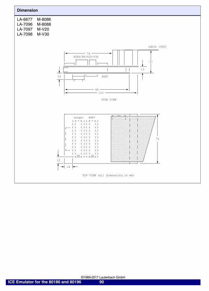
LA-6677 M-8086LA-7096 M-8088LA-7097 M-V20LA-7098 M-V30
Dimension
cable (350)
748086/88/V20/V30
37
13
10 8087
99113
SIDE VIEW
target 8087
74
12
14
TOP VIEW (all dimensions in mm)
ICE Emulator for the 80186 and 80196 90 ©1989-2017 Lauterbach GmbH

LA-6695 M-196EN
Dimension
cable (400)
86
37
13
111125
SIDE VIEW
8
1
78
TOP VIEW (all dimensions in mm)
13
13
ICE Emulator for the 80186 and 80196 91 ©1989-2017 Lauterbach GmbH

LA-6674 M-196KBLA-7080 M-196KDLA-7081 M-196KCLA-7082 M-194LA-7083 M-198
Dimension
cable (350)
65
37
13
9
92105
SIDE VIEW
26
PLCC 68
1
74
PLCC 52
136
8
13
TOP VIEW (all dimensions in mm)
ICE Emulator for the 80186 and 80196 92 ©1989-2017 Lauterbach GmbH

Adapter
No adapters necessary !
ICE Emulator for the 80186 and 80196 93 ©1989-2017 Lauterbach GmbH