Embed Size (px)
Citation preview
FN2920Rev 10.00
April 12, 2007
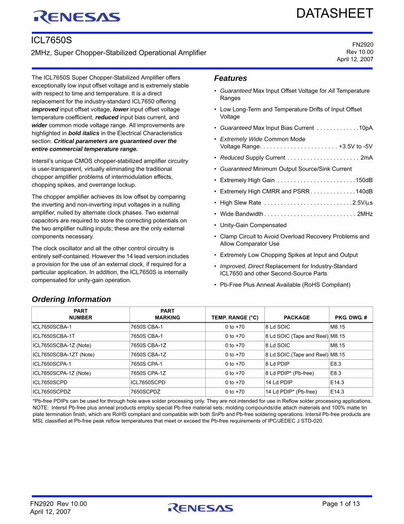
ICL7650S2MHz, Super Chopper-Stabilized Operational Amplifier
DATASHEET
The ICL7650S Super Chopper-Stabilized Amplifier offers exceptionally low input offset voltage and is extremely stable with respect to time and temperature. It is a direct replacement for the industry-standard ICL7650 offering improved input offset voltage, lower input offset voltage temperature coefficient, reduced input bias current, and wider common mode voltage range. All improvements are highlighted in bold italics in the Electrical Characteristics section. Critical parameters are guaranteed over the entire commercial temperature range.
Intersil’s unique CMOS chopper-stabilized amplifier circuitry is user-transparent, virtually eliminating the traditional chopper amplifier problems of intermodulation effects, chopping spikes, and overrange lockup.
The chopper amplifier achieves its low offset by comparing the inverting and non-inverting input voltages in a nulling amplifier, nulled by alternate clock phases. Two external capacitors are required to store the correcting potentials on the two amplifier nulling inputs; these are the only external components necessary.
The clock oscillator and all the other control circuitry is entirely self-contained. However the 14 lead version includes a provision for the use of an external clock, if required for a particular application. In addition, the ICL7650S is internally compensated for unity-gain operation.
Features
• Guaranteed Max Input Offset Voltage for All Temperature Ranges
• Low Long-Term and Temperature Drifts of Input Offset Voltage
• Guaranteed Max Input Bias Current . . . . . . . . . . . . .10pA
• Extremely Wide Common Mode Voltage Range. . . . . . . . . . . . . . . . . . . . . . . +3.5V to -5V
• Reduced Supply Current . . . . . . . . . . . . . . . . . . . . . . 2mA
• Guaranteed Minimum Output Source/Sink Current
• Extremely High Gain . . . . . . . . . . . . . . . . . . . . . . . .150dB
• Extremely High CMRR and PSRR . . . . . . . . . . . . . .140dB
• High Slew Rate . . . . . . . . . . . . . . . . . . . . . . . . . . . 2.5V/s
• Wide Bandwidth . . . . . . . . . . . . . . . . . . . . . . . . . . . . 2MHz
• Unity-Gain Compensated
• Clamp Circuit to Avoid Overload Recovery Problems and Allow Comparator Use
• Extremely Low Chopping Spikes at Input and Output
• Improved, Direct Replacement for Industry-Standard ICL7650 and other Second-Source Parts
• Pb-Free Plus Anneal Available (RoHS Compliant)
Ordering InformationPART
NUMBERPART
MARKING TEMP. RANGE (°C) PACKAGE PKG. DWG. #
ICL7650SCBA-1 7650S CBA-1 0 to +70 8 Ld SOIC M8.15
ICL7650SCBA-1T 7650S CBA-1 0 to +70 8 Ld SOIC (Tape and Reel) M8.15
ICL7650SCBA-1Z (Note) 7650S CBA-1Z 0 to +70 8 Ld SOIC M8.15
ICL7650SCBA-1ZT (Note) 7650S CBA-1Z 0 to +70 8 Ld SOIC (Tape and Reel) M8.15
ICL7650SCPA-1 7650S CPA-1 0 to +70 8 Ld PDIP E8.3
ICL7650SCPA-1Z (Note) 7650S CPA-1Z 0 to +70 8 Ld PDIP* (Pb-free) E8.3
ICL7650SCPD ICL7650SCPD 0 to +70 14 Ld PDIP E14.3
ICL7650SCPDZ 7650SCPDZ 0 to +70 14 Ld PDIP* (Pb-free) E14.3
*Pb-free PDIPs can be used for through hole wave solder processing only. They are not intended for use in Reflow solder processing applications.NOTE: Intersil Pb-free plus anneal products employ special Pb-free material sets; molding compounds/die attach materials and 100% matte tin plate termination finish, which are RoHS compliant and compatible with both SnPb and Pb-free soldering operations. Intersil Pb-free products are MSL classified at Pb-free peak reflow temperatures that meet or exceed the Pb-free requirements of IPC/JEDEC J STD-020.
FN2920 Rev 10.00 Page 1 of 13April 12, 2007
ICL7650S
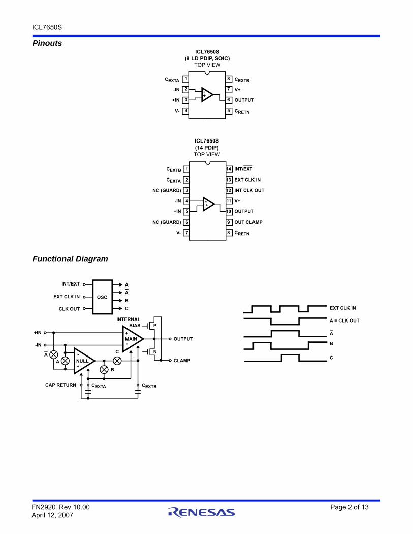
PinoutsICL7650S
(8 LD PDIP, SOIC)TOP VIEW
CEXTA
-IN
+IN
V-
1
2
3
4
8
7
6
5
CEXTB
V+
OUTPUT
CRETN
-+
ICL7650S(14 PDIP)TOP VIEW
CEXTB
CEXTA
NC (GUARD)
-IN
+IN
NC (GUARD)
V-
INT/EXT
EXT CLK IN
INT CLK OUT
V+
OUTPUT
OUT CLAMP
CRETN
1
2
3
4
5
6
7
14
13
12
11
10
9
8
-+
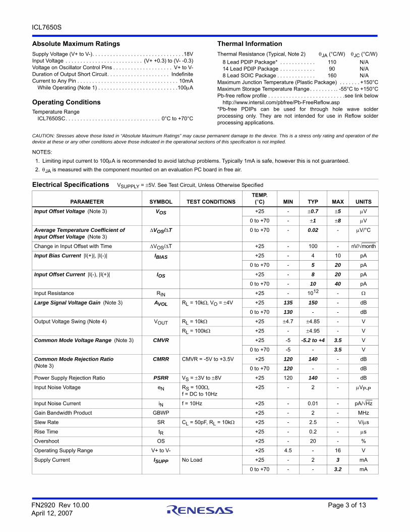
Functional Diagram
OSC.
MAIN
NULL
+
-
+
-
+IN
-IN
A
CAP RETURN CEXTA CEXTB
A
B
C
CLAMP
OUTPUT
N
PINTERNAL
BIAS
A
A
B
C
INT/EXT
EXT CLK IN
CLK OUT EXT CLK IN
A = CLK OUT
A
B
C
FN2920 Rev 10.00 Page 2 of 13April 12, 2007
ICL7650S
Absolute Maximum Ratings Thermal Information
Supply Voltage (V+ to V-). . . . . . . . . . . . . . . . . . . . . . . . . . . . . . .18VInput Voltage . . . . . . . . . . . . . . . . . . . . . . . . . . (V+ +0.3) to (V- -0.3)Voltage on Oscillator Control Pins . . . . . . . . . . . . . . . . . . . . V+ to V-Duration of Output Short Circuit. . . . . . . . . . . . . . . . . . . . . IndefiniteCurrent to Any Pin . . . . . . . . . . . . . . . . . . . . . . . . . . . . . . . . . . 10mA
While Operating (Note 1) . . . . . . . . . . . . . . . . . . . . . . . . . . .100A
Operating ConditionsTemperature Range
ICL7650SC. . . . . . . . . . . . . . . . . . . . . . . . . . . . . . . . 0°C to +70°C
Thermal Resistance (Typical, Note 2) JA (°C/W) JC (°C/W)
8 Lead PDIP Package* . . . . . . . . . . . . 110 N/A14 Lead PDIP Package . . . . . . . . . . . . 90 N/A8 Lead SOIC Package . . . . . . . . . . . . . 160 N/A
Maximum Junction Temperature (Plastic Package) . . . . . . . +150°CMaximum Storage Temperature Range . . . . . . . . . . -55°C to +150°CPb-free reflow profile . . . . . . . . . . . . . . . . . . . . . . . . . .see link below
http://www.intersil.com/pbfree/Pb-FreeReflow.asp*Pb-free PDIPs can be used for through hole wave solderprocessing only. They are not intended for use in Reflow solderprocessing applications.
CAUTION: Stresses above those listed in “Absolute Maximum Ratings” may cause permanent damage to the device. This is a stress only rating and operation of thedevice at these or any other conditions above those indicated in the operational sections of this specification is not implied.
NOTES:
1. Limiting input current to 100A is recommended to avoid latchup problems. Typically 1mA is safe, however this is not guaranteed.
2. JA is measured with the component mounted on an evaluation PC board in free air.
Electrical Specifications VSUPPLY = 5V. See Test Circuit, Unless Otherwise Specified
PARAMETER SYMBOL TEST CONDITIONSTEMP.
(°C) MIN TYP MAX UNITS
Input Offset Voltage (Note 3) VOS +25 - 0.7 5 V
0 to +70 - 1 8 V
Average Temperature Coefficient of Input Offset Voltage (Note 3)
VOS/T 0 to +70 - 0.02 - V/°C
Change in Input Offset with Time VOS/T +25 - 100 - nV/month
Input Bias Current |I(+)|, |I(-)| IBIAS +25 - 4 10 pA
0 to +70 - 5 20 pA
Input Offset Current |I(-), |I(+)| IOS +25 - 8 20 pA
0 to +70 - 10 40 pA
Input Resistance RIN +25 - 1012 -
Large Signal Voltage Gain (Note 3) AVOL RL = 10k, VO = 4V +25 135 150 - dB
0 to +70 130 - - dB
Output Voltage Swing (Note 4) VOUT RL = 10k +25 4.7 4.85 - V
RL = 100k +25 - 4.95 - V
Common Mode Voltage Range (Note 3) CMVR +25 -5 -5.2 to +4 3.5 V
0 to +70 -5 - 3.5 V
Common Mode Rejection Ratio (Note 3)
CMRR CMVR = -5V to +3.5V +25 120 140 - dB
0 to +70 120 - - dB
Power Supply Rejection Ratio PSRR VS = 3V to 8V +25 120 140 - dB
Input Noise Voltage eN RS = 100,f = DC to 10Hz
+25 - 2 - VP-P
Input Noise Current iN f = 10Hz +25 - 0.01 - pA/Hz
Gain Bandwidth Product GBWP +25 - 2 - MHz
Slew Rate SR CL = 50pF, RL = 10k +25 - 2.5 - V/s
Rise Time tR +25 - 0.2 - s
Overshoot OS +25 - 20 - %
Operating Supply Range V+ to V- +25 4.5 - 16 V
Supply Current ISUPP No Load +25 - 2 3 mA
0 to +70 - - 3.2 mA
FN2920 Rev 10.00 Page 3 of 13April 12, 2007
ICL7650S
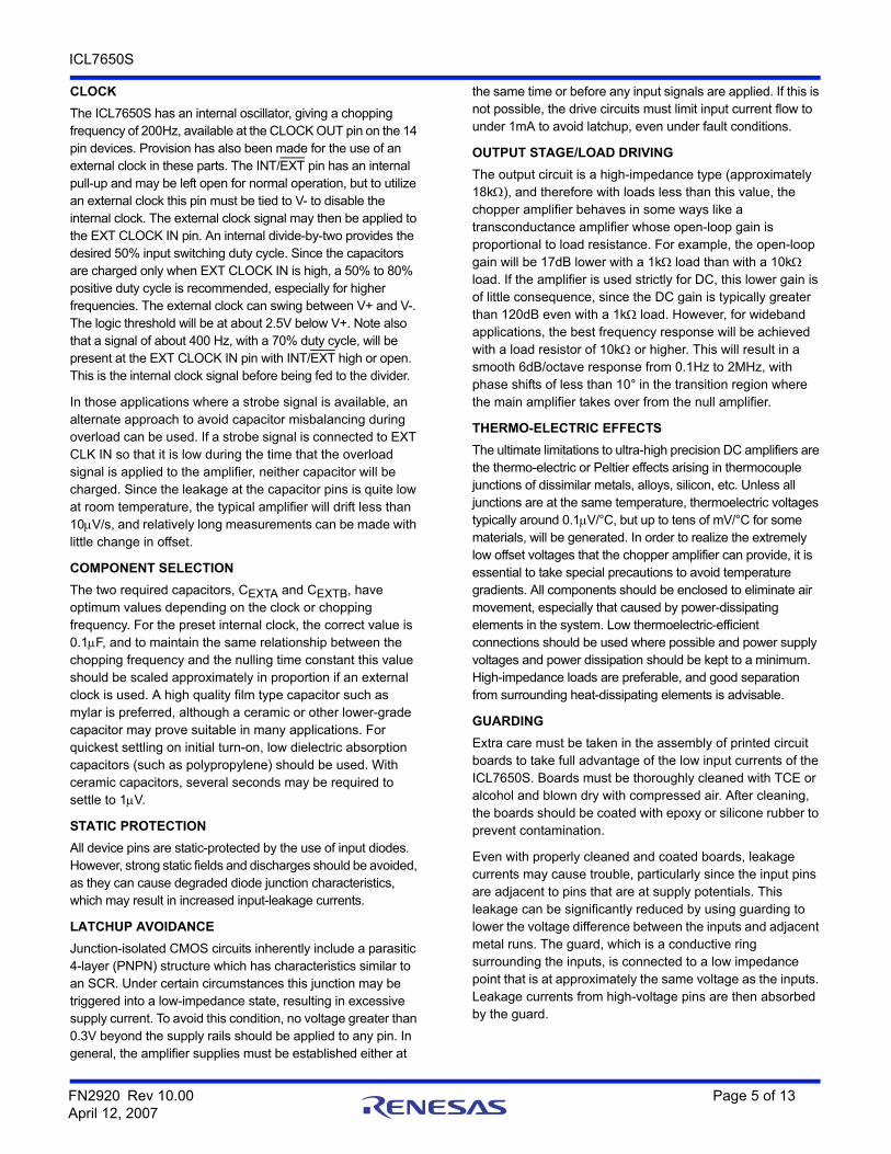
Test Circuit
Application Information
Detailed Description
AMPLIFIER
The functional diagram shows the major elements of the ICL7650S. There are two amplifiers, the main amplifier, and the nulling amplifier. Both have offset-null capability. The main amplifier is connected continuously from the input to the output, while the nulling amplifier, under the control of the chopping oscillator and clock circuit, alternately nulls itself and the main amplifier. The nulling connections, which are MOSFET gates, are inherently high impedance, and two external capacitors provide the required storage of the nulling potentials and the necessary nulling-loop time constants. The nulling arrangement operates over the full common-mode and power-supply ranges, and is also independent of the output level, thus giving exceptionally high CMRR, PSRR, and AVOL.
Careful balancing of the input switches, and the inherent balance of the input circuit, minimizes chopper frequency charge injection at the input terminals, and also the feed forward-type injection into the compensation capacitor, which is the main cause of output spikes in this type of circuit.
INTERMODULATION
Previous chopper-stabilized amplifiers have suffered from intermodulation effects between the chopper frequency and input signals. These arise because the finite AC gain of the amplifier necessitates a small AC signal at the input. This is seen by the zeroing circuit as an error signal, which is chopped and fed back, thus injecting sum and difference frequencies and causing disturbances to the gain and phase vs frequency characteristics near the chopping frequency. These effects are substantially reduced in the ICL7650S by feeding the nulling circuit with a dynamic current, corresponding to the compensation capacitor current, in such a way as to cancel that portion of the input signal due to finite AC gain. Since that is the major error contribution to the ICL7650S, the intermodulation and gain/phase disturbances are held to very low values, and can generally be ignored.
CAPACITOR CONNECTION
The null/storage capacitors should be connected to the CEXTA and CEXTB pins, with a common connection to the CRETN pin. This connection should be made directly by either a separate wire or PC trace to avoid injecting load current IR drops into the capacitive circuitry. The outside foil, where available, should be connected to CRETN.
OUTPUT CLAMP
The OUTPUT CLAMP pin allows reduction of the overload recovery time inherent with chopper-stabilized amplifiers. When tied to the inverting input pin, or summing junction, a current path between this point and the OUTPUT pin occurs just before the device output saturates. Thus uncontrolled input differentials are avoided, together with the consequent charge buildup on the correction-storage capacitors. The output swing is slightly reduced.
Output Source Current IO SOURCE +25 2.9 4.5 - mA
0 to +70 2.3 - - mA
Output Sink Current IO SINK +25 25 30 - mA
0 to +70 20 - - mA
Internal Chopping Frequency fCH Pins 13 and 14 Open +25 120 250 375 Hz
Clamp ON Current (Note 5) RL = 100k +25 25 70 - A
Clamp OFF Current (Note 5) -4V VOUT +4V +25 - 0.001 5 nA
0 to +70 - - 10 nA
NOTES:
3. These parameters are guaranteed by design and characterization, but not tested at temperature extremes because thermocouple effects prevent precise measurement of these voltages in automatic test equipment.
4. OUTPUT CLAMP not connected. See typical characteristic curves for output swing vs clamp current characteristics.5. See OUTPUT CLAMP under detailed description.6. All significant improvements over the industry-standard ICL7650 are highlighted in bold italics.
Electrical Specifications VSUPPLY = 5V. See Test Circuit, Unless Otherwise Specified (Continued)
PARAMETER SYMBOL TEST CONDITIONSTEMP.
(°C) MIN TYP MAX UNITS
ICL7650S
+
-
OUTPUT
R21M
CCR
0.1F 0.1F
C
R11M
FN2920 Rev 10.00 Page 4 of 13April 12, 2007
ICL7650S
CLOCK
The ICL7650S has an internal oscillator, giving a chopping frequency of 200Hz, available at the CLOCK OUT pin on the 14 pin devices. Provision has also been made for the use of an external clock in these parts. The INT/EXT pin has an internal pull-up and may be left open for normal operation, but to utilize an external clock this pin must be tied to V- to disable the internal clock. The external clock signal may then be applied to the EXT CLOCK IN pin. An internal divide-by-two provides the desired 50% input switching duty cycle. Since the capacitors are charged only when EXT CLOCK IN is high, a 50% to 80% positive duty cycle is recommended, especially for higher frequencies. The external clock can swing between V+ and V-. The logic threshold will be at about 2.5V below V+. Note also that a signal of about 400 Hz, with a 70% duty cycle, will be present at the EXT CLOCK IN pin with INT/EXT high or open. This is the internal clock signal before being fed to the divider.
In those applications where a strobe signal is available, an alternate approach to avoid capacitor misbalancing during overload can be used. If a strobe signal is connected to EXT CLK IN so that it is low during the time that the overload signal is applied to the amplifier, neither capacitor will be charged. Since the leakage at the capacitor pins is quite low at room temperature, the typical amplifier will drift less than 10V/s, and relatively long measurements can be made with little change in offset.
COMPONENT SELECTION
The two required capacitors, CEXTA and CEXTB, have optimum values depending on the clock or chopping frequency. For the preset internal clock, the correct value is 0.1F, and to maintain the same relationship between the chopping frequency and the nulling time constant this value should be scaled approximately in proportion if an external clock is used. A high quality film type capacitor such as mylar is preferred, although a ceramic or other lower-grade capacitor may prove suitable in many applications. For quickest settling on initial turn-on, low dielectric absorption capacitors (such as polypropylene) should be used. With ceramic capacitors, several seconds may be required to settle to 1V.
STATIC PROTECTION
All device pins are static-protected by the use of input diodes. However, strong static fields and discharges should be avoided, as they can cause degraded diode junction characteristics, which may result in increased input-leakage currents.
LATCHUP AVOIDANCE
Junction-isolated CMOS circuits inherently include a parasitic 4-layer (PNPN) structure which has characteristics similar to an SCR. Under certain circumstances this junction may be triggered into a low-impedance state, resulting in excessive supply current. To avoid this condition, no voltage greater than 0.3V beyond the supply rails should be applied to any pin. In general, the amplifier supplies must be established either at
the same time or before any input signals are applied. If this is not possible, the drive circuits must limit input current flow to under 1mA to avoid latchup, even under fault conditions.
OUTPUT STAGE/LOAD DRIVING
The output circuit is a high-impedance type (approximately 18k), and therefore with loads less than this value, the chopper amplifier behaves in some ways like a transconductance amplifier whose open-loop gain is proportional to load resistance. For example, the open-loop gain will be 17dB lower with a 1k load than with a 10k load. If the amplifier is used strictly for DC, this lower gain is of little consequence, since the DC gain is typically greater than 120dB even with a 1k load. However, for wideband applications, the best frequency response will be achieved with a load resistor of 10k or higher. This will result in a smooth 6dB/octave response from 0.1Hz to 2MHz, with phase shifts of less than 10° in the transition region where the main amplifier takes over from the null amplifier.
THERMO-ELECTRIC EFFECTS
The ultimate limitations to ultra-high precision DC amplifiers are the thermo-electric or Peltier effects arising in thermocouple junctions of dissimilar metals, alloys, silicon, etc. Unless all junctions are at the same temperature, thermoelectric voltages typically around 0.1V/°C, but up to tens of mV/°C for some materials, will be generated. In order to realize the extremely low offset voltages that the chopper amplifier can provide, it is essential to take special precautions to avoid temperature gradients. All components should be enclosed to eliminate air movement, especially that caused by power-dissipating elements in the system. Low thermoelectric-efficient connections should be used where possible and power supply voltages and power dissipation should be kept to a minimum. High-impedance loads are preferable, and good separation from surrounding heat-dissipating elements is advisable.
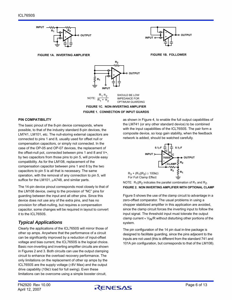
GUARDING
Extra care must be taken in the assembly of printed circuit boards to take full advantage of the low input currents of the ICL7650S. Boards must be thoroughly cleaned with TCE or alcohol and blown dry with compressed air. After cleaning, the boards should be coated with epoxy or silicone rubber to prevent contamination.
Even with properly cleaned and coated boards, leakage currents may cause trouble, particularly since the input pins are adjacent to pins that are at supply potentials. This leakage can be significantly reduced by using guarding to lower the voltage difference between the inputs and adjacent metal runs. The guard, which is a conductive ring surrounding the inputs, is connected to a low impedance point that is at approximately the same voltage as the inputs. Leakage currents from high-voltage pins are then absorbed by the guard.
FN2920 Rev 10.00 Page 5 of 13April 12, 2007
ICL7650S
PIN COMPATIBILITY
The basic pinout of the 8-pin device corresponds, where possible, to that of the industry standard 8-pin devices, the LM741, LM101, etc. The null-storing external capacitors are connected to pins 1 and 8, usually used for offset null or compensation capacitors, or simply not connected. In the case of the OP-05 and OP-07 devices, the replacement of the offset-null pot, connected between pins 1 and 8 and V+, by two capacitors from those pins to pin 5, will provide easy compatibility. As for the LM108, replacement of the compensation capacitor between pins 1 and 8 by the two capacitors to pin 5 is all that is necessary. The same operation, with the removal of any connection to pin 5, will suffice for the LM101, A748, and similar parts.
The 14-pin device pinout corresponds most closely to that of the LM108 device, owing to the provision of “NC” pins for guarding between the input and all other pins. Since this device does not use any of the extra pins, and has no provision for offset-nulling, but requires a compensation capacitor, some changes will be required in layout to convert it to the ICL7650S.
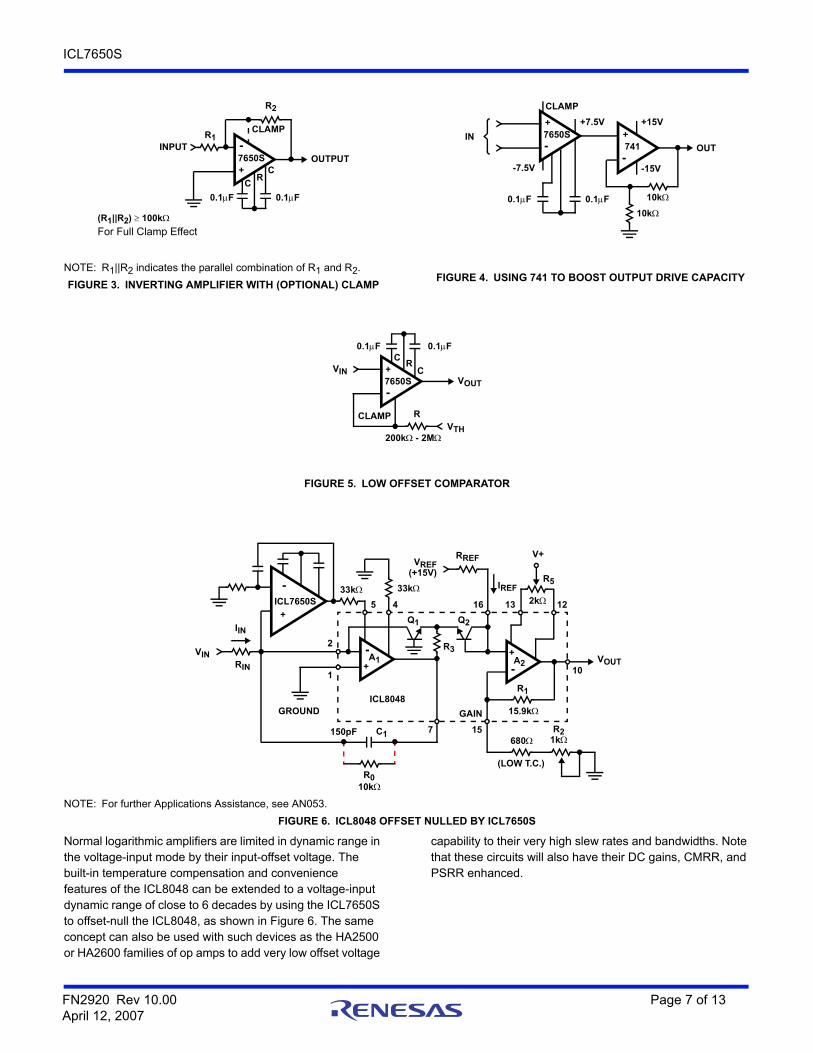
Typical ApplicationsClearly the applications of the ICL7650S will mirror those of other op amps. Anywhere that the performance of a circuit can be significantly improved by a reduction of input-offset voltage and bias current, the ICL7650S is the logical choice. Basic non-inverting and inverting amplifier circuits are shown in Figures 2 and 3. Both circuits can use the output clamping circuit to enhance the overload recovery performance. The only limitations on the replacement of other op amps by the ICL7650S are the supply voltage (8V Max) and the output drive capability (10k load for full swing). Even these limitations can be overcome using a simple booster circuit,
as shown in Figure 4, to enable the full output capabilities of the LM741 (or any other standard device) to be combined with the input capabilities of the ICL7650S. The pair form a composite device, so loop gain stability, when the feedback network is added, should be watched carefully.
Figure 5 shows the use of the clamp circuit to advantage in a zero-offset comparator. The usual problems in using a chopper stabilized amplifier in this application are avoided, since the clamp circuit forces the inverting input to follow the input signal. The threshold input must tolerate the output clamp current VlN/R without disturbing other portions of the system.
The pin configuration of the 14 pin dual in-line package is designed to facilitate guarding, since the pins adjacent to the inputs are not used (this is different from the standard 741 and 101A pin configuration, but corresponds to that of the LM108).
FIGURE 1A. INVERTING AMPLIFIER FIGURE 1B. FOLLOWER
FIGURE 1C. NON-INVERTING AMPLIFIER
FIGURE 1. CONNECTION OF INPUT GUARDS
+
-
INPUTR1 R2
OUTPUT +
-
INPUTOUTPUT
+
-
INPUT
R1
R2
OUTPUT
R1 R2R1 R2+----------------------NOTE:
SHOULD BE LOWIMPEDANCE FOROPTIMUM GUARDING
7650S+
-
0.1F
OUTPUTC
RC
R2
R1R3
CLAMP
INPUT
0.1F
R3 + (R1||R2) 100kFor Full Clamp Effect
NOTE: R1||R2 indicates the parallel combination of R1 and R2.
FIGURE 2. NON INVERTING AMPLIFIER WITH OPTIONAL CLAMP
FN2920 Rev 10.00 Page 6 of 13April 12, 2007
ICL7650S
Normal logarithmic amplifiers are limited in dynamic range in the voltage-input mode by their input-offset voltage. The built-in temperature compensation and convenience features of the ICL8048 can be extended to a voltage-input dynamic range of close to 6 decades by using the ICL7650S to offset-null the ICL8048, as shown in Figure 6. The same concept can also be used with such devices as the HA2500 or HA2600 families of op amps to add very low offset voltage
capability to their very high slew rates and bandwidths. Note that these circuits will also have their DC gains, CMRR, and PSRR enhanced.
7650S+
-
0.1F
OUTPUTC
RC
R2
R1CLAMP
INPUT
0.1F
(R1||R2) 100kFor Full Clamp Effect
7650S-
+
0.1F
OUT
CLAMP
IN
0.1F
741-
+
-7.5V
+7.5V +15V
-15V
10k
10k
NOTE: R1||R2 indicates the parallel combination of R1 and R2.
FIGURE 3. INVERTING AMPLIFIER WITH (OPTIONAL) CLAMPFIGURE 4. USING 741 TO BOOST OUTPUT DRIVE CAPACITY
7650S+
-
0.1F
VOUT
CR
C
CLAMP
VIN
0.1F
VTH200k - 2M
R
FIGURE 5. LOW OFFSET COMPARATOR
A1+
- +
-A2
ICL7650S
+
-
VOUT
R1
15.9k
680R2
GROUND
RREF
R3
Q1
2k
V+
Q2
R5
VREF
IREF
GAIN
33k33k
150pF C1
R010k
(LOW T.C.)
IIN
RIN
VIN
7 15
10
121316
(+15V)
1k
45
2
1
ICL8048
NOTE: For further Applications Assistance, see AN053.
FIGURE 6. ICL8048 OFFSET NULLED BY ICL7650S
FN2920 Rev 10.00 Page 7 of 13April 12, 2007
ICL7650S
Typical Performance Curves
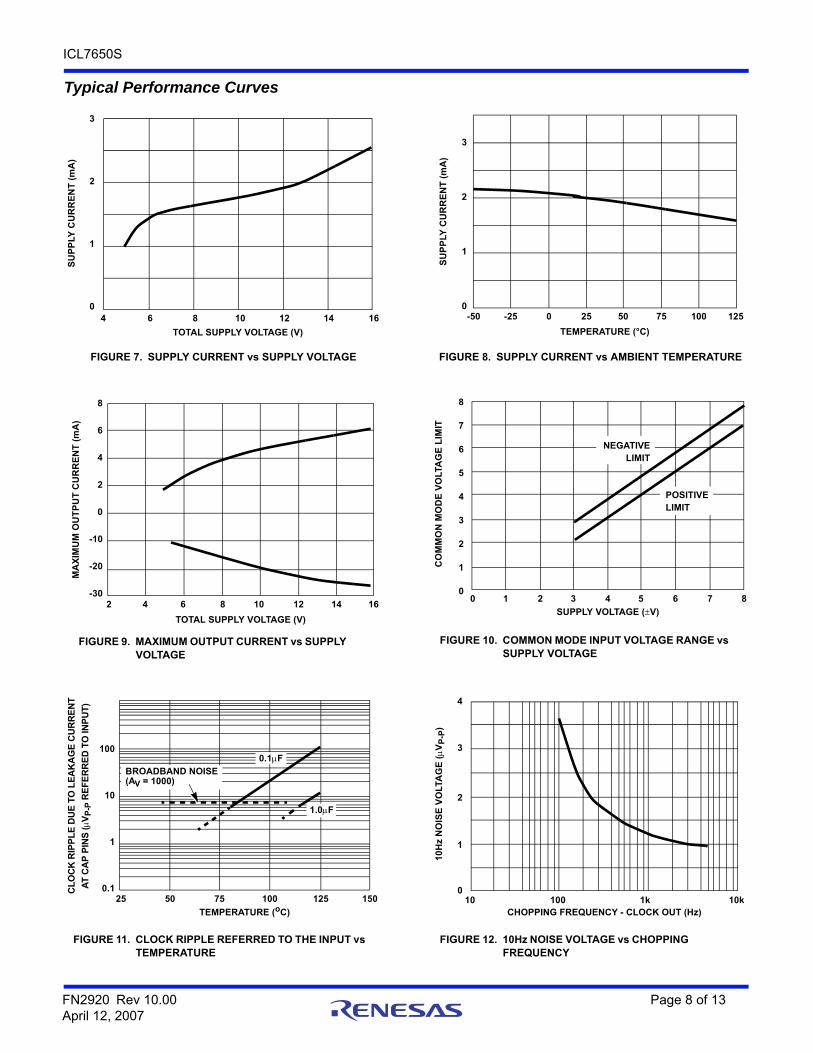
FIGURE 7. SUPPLY CURRENT vs SUPPLY VOLTAGE FIGURE 8. SUPPLY CURRENT vs AMBIENT TEMPERATURE
FIGURE 9. MAXIMUM OUTPUT CURRENT vs SUPPLY VOLTAGE
FIGURE 10. COMMON MODE INPUT VOLTAGE RANGE vs SUPPLY VOLTAGE
FIGURE 11. CLOCK RIPPLE REFERRED TO THE INPUT vs TEMPERATURE
FIGURE 12. 10Hz NOISE VOLTAGE vs CHOPPING FREQUENCY
3
2
1
04
SU
PP
LY C
UR
RE
NT
(m
A)
6 8 10 12 14 16
TOTAL SUPPLY VOLTAGE (V)
SU
PP
LY C
UR
RE
NT
(m
A)
3
2
1
0-50 -25 0 25 50 75 100 125
TEMPERATURE (°C)
MA
XIM
UM
OU
TP
UT
CU
RR
EN
T (
mA
)
8
6
4
2
0
-10
-20
-302 4 6 8 10 12 14 16
TOTAL SUPPLY VOLTAGE (V)SUPPLY VOLTAGE (V)
CO
MM
ON
MO
DE
VO
LTA
GE
LIM
IT
8
7
6
5
4
3
2
1
00 1 2 3 4 5 6 7 8
POSITIVELIMIT
NEGATIVELIMIT
CL
OC
K R
IPP
LE
DU
E T
O L
EA
KA
GE
CU
RR
EN
T
AT
CA
P P
INS
(V
P-P
RE
FE
RR
ED
TO
INP
UT
)
TEMPERATURE (oC)
100
10
1
0.125 50 75 100 125 150
BROADBAND NOISE(AV = 1000)
0.1F
1.0F
CHOPPING FREQUENCY - CLOCK OUT (Hz)
10
Hz
NO
ISE
VO
LTA
GE
(V
P-P
)
4
3
2
1
10 100 1k 10k0
FN2920 Rev 10.00 Page 8 of 13April 12, 2007
ICL7650S
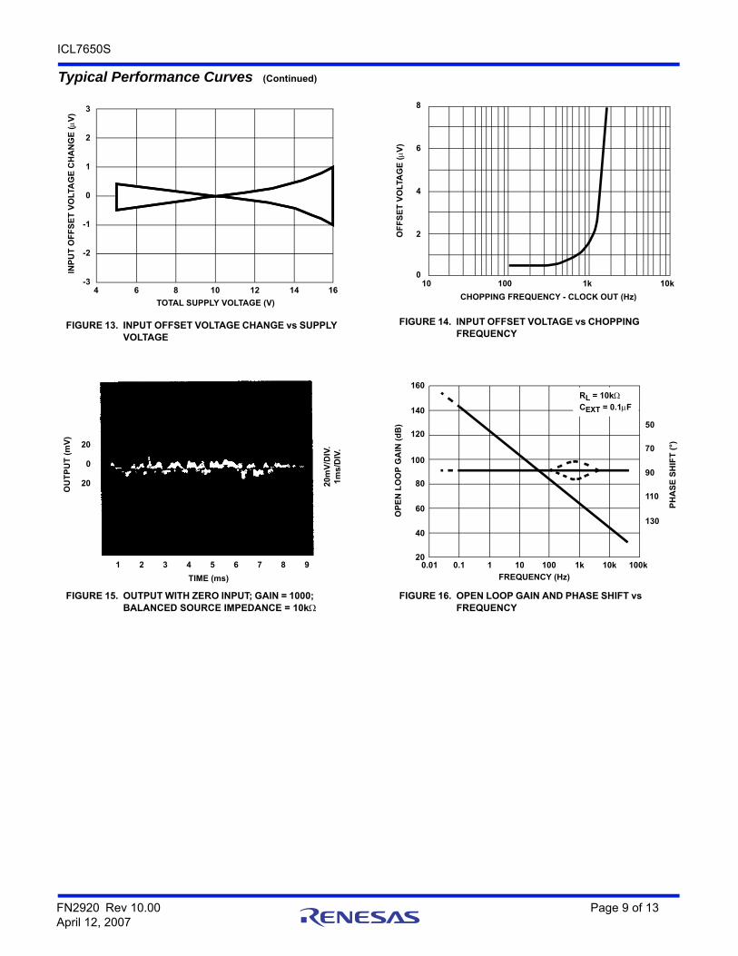
FIGURE 13. INPUT OFFSET VOLTAGE CHANGE vs SUPPLY VOLTAGE
FIGURE 14. INPUT OFFSET VOLTAGE vs CHOPPING FREQUENCY
FIGURE 15. OUTPUT WITH ZERO INPUT; GAIN = 1000; BALANCED SOURCE IMPEDANCE = 10k
FIGURE 16. OPEN LOOP GAIN AND PHASE SHIFT vs FREQUENCY
Typical Performance Curves (Continued)IN
PU
T O
FF
SE
T V
OLT
AG
E C
HA
NG
E (V
)
TOTAL SUPPLY VOLTAGE (V)
3
2
1
0
-1
-2
-34 6 8 10 12 14 16
OF
FS
ET
VO
LTA
GE
(V
)
CHOPPING FREQUENCY - CLOCK OUT (Hz)
8
6
4
2
10 100 1k 10k0
TIME (ms)
OU
TP
UT
(m
V)
20
0
20
1 2 3 4 5 6 7 8 9
20m
V/D
IV.
1m
s/D
IV.
OP
EN
LO
OP
GA
IN (
dB
)
FREQUENCY (Hz)
PH
AS
E S
HIF
T (
°)
160
140
120
100
80
60
40
0.01 0.1 1 10 100 1k 10k 100k
130
110
90
70
50
20
RL = 10kCEXT = 0.1F
FN2920 Rev 10.00 Page 9 of 13April 12, 2007
ICL7650S
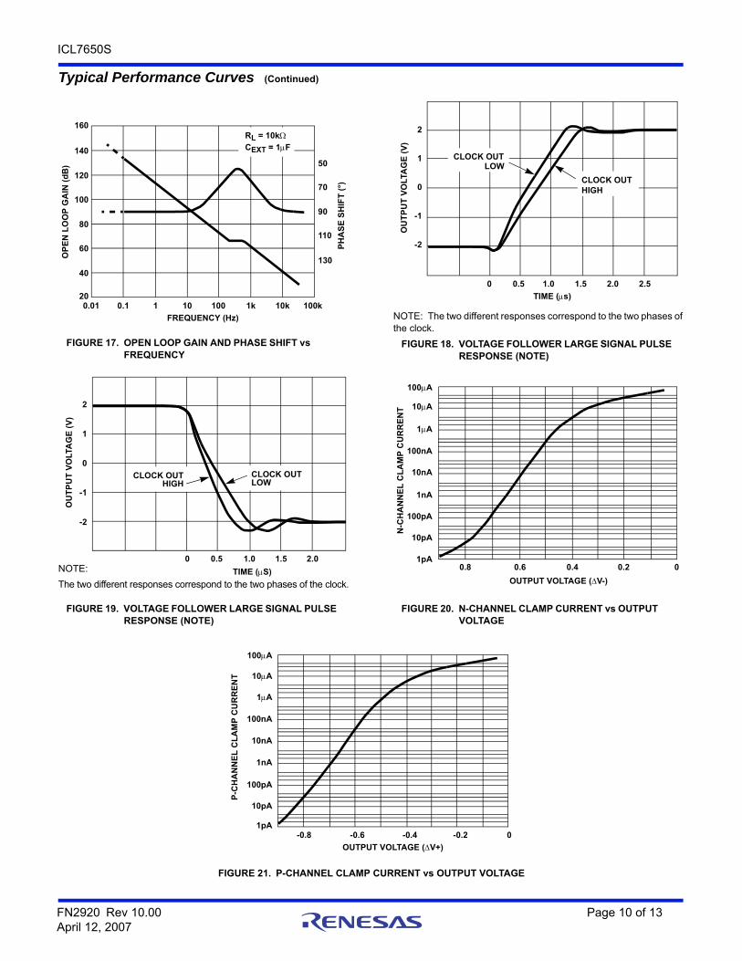
FIGURE 17. OPEN LOOP GAIN AND PHASE SHIFT vs FREQUENCY
NOTE: The two different responses correspond to the two phases of the clock.
FIGURE 18. VOLTAGE FOLLOWER LARGE SIGNAL PULSE RESPONSE (NOTE)
FIGURE 19. VOLTAGE FOLLOWER LARGE SIGNAL PULSE RESPONSE (NOTE)
FIGURE 20. N-CHANNEL CLAMP CURRENT vs OUTPUT VOLTAGE
FIGURE 21. P-CHANNEL CLAMP CURRENT vs OUTPUT VOLTAGE
Typical Performance Curves (Continued)
PH
AS
E S
HIF
T (
°)
OP
EN
LO
OP
GA
IN (
dB
)
FREQUENCY (Hz)
0.01 0.1 1 10 100 1k 10k 100k
130
110
90
70
50
RL = 10kCEXT = 1F
160
140
120
100
80
60
40
20 TIME (s)
0 0.5 1.0 1.5 2.0 2.5
OU
TP
UT
VO
LTA
GE
(V
)
2
1
0
-1
-2
CLOCK OUTHIGH
CLOCK OUTLOW
TIME (S)
OU
TP
UT
VO
LTA
GE
(V
)
2
1
0
-1
-2
0 0.5 1.0 1.5 2.0
CLOCK OUTHIGH
CLOCK OUTLOW
NOTE:
The two different responses correspond to the two phases of the clock.
N-C
HA
NN
EL
CL
AM
P C
UR
RE
NT
OUTPUT VOLTAGE (V-)
100A
10A
1A
100nA
10nA
1nA
100pA
10pA
1pA0.8 0.6 0.4 0.2 0
P-C
HA
NN
EL
CL
AM
P C
UR
RE
NT
OUTPUT VOLTAGE (V+)
100A
10A
1A
100nA
10nA
1nA
100pA
10pA
1pA-0.8 -0.6 -0.4 -0.2 0
FN2920 Rev 10.00 Page 10 of 13April 12, 2007
ICL7650S
FN2920 Rev 10.00 Page 11 of 13April 12, 2007
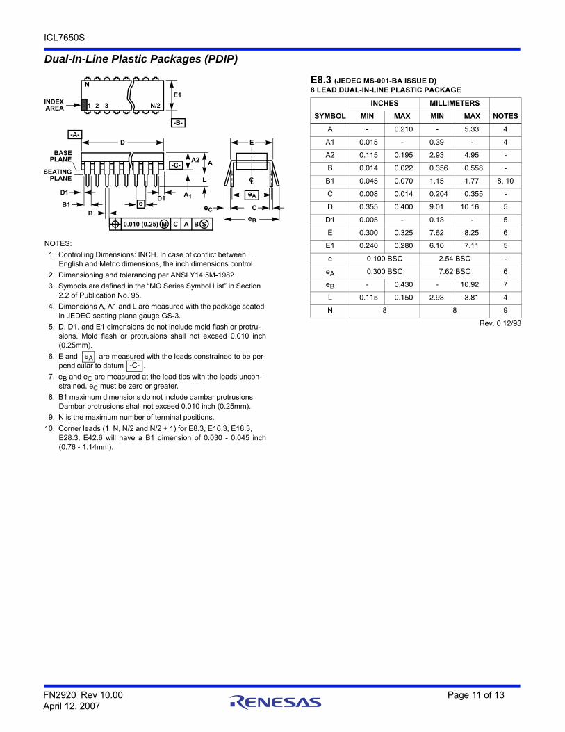
Dual-In-Line Plastic Packages (PDIP)
CL
E
eA
C
eB
eC
-B-
E1INDEX
1 2 3 N/2
N
AREA
SEATING
BASEPLANE
PLANE
-C-
D1
B1B
e
D
D1
AA2
L
A1
-A-
0.010 (0.25) C AM B S
NOTES:
1. Controlling Dimensions: INCH. In case of conflict between English and Metric dimensions, the inch dimensions control.
2. Dimensioning and tolerancing per ANSI Y14.5M-1982.
3. Symbols are defined in the “MO Series Symbol List” in Section 2.2 of Publication No. 95.
4. Dimensions A, A1 and L are measured with the package seated in JEDEC seating plane gauge GS-3.
5. D, D1, and E1 dimensions do not include mold flash or protru-sions. Mold flash or protrusions shall not exceed 0.010 inch(0.25mm).
6. E and are measured with the leads constrained to be per-pendicular to datum .
7. eB and eC are measured at the lead tips with the leads uncon-strained. eC must be zero or greater.
8. B1 maximum dimensions do not include dambar protrusions. Dambar protrusions shall not exceed 0.010 inch (0.25mm).
9. N is the maximum number of terminal positions.
10. Corner leads (1, N, N/2 and N/2 + 1) for E8.3, E16.3, E18.3, E28.3, E42.6 will have a B1 dimension of 0.030 - 0.045 inch(0.76 - 1.14mm).
eA-C-
E8.3 (JEDEC MS-001-BA ISSUE D)8 LEAD DUAL-IN-LINE PLASTIC PACKAGE
SYMBOL
INCHES MILLIMETERS
NOTESMIN MAX MIN MAX
A - 0.210 - 5.33 4
A1 0.015 - 0.39 - 4
A2 0.115 0.195 2.93 4.95 -
B 0.014 0.022 0.356 0.558 -
B1 0.045 0.070 1.15 1.77 8, 10
C 0.008 0.014 0.204 0.355 -
D 0.355 0.400 9.01 10.16 5
D1 0.005 - 0.13 - 5
E 0.300 0.325 7.62 8.25 6
E1 0.240 0.280 6.10 7.11 5
e 0.100 BSC 2.54 BSC -
eA 0.300 BSC 7.62 BSC 6
eB - 0.430 - 10.92 7
L 0.115 0.150 2.93 3.81 4
N 8 8 9
Rev. 0 12/93
ICL7650S
FN2920 Rev 10.00 Page 12 of 13April 12, 2007
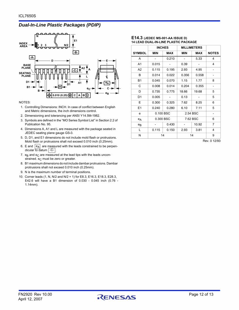
Dual-In-Line Plastic Packages (PDIP)
NOTES:
1. Controlling Dimensions: INCH. In case of conflict between English and Metric dimensions, the inch dimensions control.
2. Dimensioning and tolerancing per ANSI Y14.5M-1982.
3. Symbols are defined in the “MO Series Symbol List” in Section 2.2 of Publication No. 95.
4. Dimensions A, A1 and L are measured with the package seated in JEDEC seating plane gauge GS-3.
5. D, D1, and E1 dimensions do not include mold flash or protrusions. Mold flash or protrusions shall not exceed 0.010 inch (0.25mm).
6. E and are measured with the leads constrained to be perpen-dicular to datum .
7. eB and eC are measured at the lead tips with the leads uncon-strained. eC must be zero or greater.
8. B1 maximum dimensions do not include dambar protrusions. Dambar protrusions shall not exceed 0.010 inch (0.25mm).
9. N is the maximum number of terminal positions.
10. Corner leads (1, N, N/2 and N/2 + 1) for E8.3, E16.3, E18.3, E28.3, E42.6 will have a B1 dimension of 0.030 - 0.045 inch (0.76 -1.14mm).
eA-C-
CL
E
eA
C
eB
eC
-B-
E1INDEX
1 2 3 N/2
N
AREA
SEATING
BASEPLANE
PLANE
-C-
D1
B1B
e
D
D1
AA2
L
A1
-A-
0.010 (0.25) C AM B S
E14.3 (JEDEC MS-001-AA ISSUE D)14 LEAD DUAL-IN-LINE PLASTIC PACKAGE
SYMBOL
INCHES MILLIMETERS
NOTESMIN MAX MIN MAX
A - 0.210 - 5.33 4
A1 0.015 - 0.39 - 4
A2 0.115 0.195 2.93 4.95 -
B 0.014 0.022 0.356 0.558 -
B1 0.045 0.070 1.15 1.77 8
C 0.008 0.014 0.204 0.355 -
D 0.735 0.775 18.66 19.68 5
D1 0.005 - 0.13 - 5
E 0.300 0.325 7.62 8.25 6
E1 0.240 0.280 6.10 7.11 5
e 0.100 BSC 2.54 BSC -
eA 0.300 BSC 7.62 BSC 6
eB - 0.430 - 10.92 7
L 0.115 0.150 2.93 3.81 4
N 14 14 9
Rev. 0 12/93
FN2920 Rev 10.00 Page 13 of 13April 12, 2007
ICL7650S
Intersil products are manufactured, assembled and tested utilizing ISO9001 quality systems as notedin the quality certifications found at www.intersil.com/en/support/qualandreliability.html
Intersil products are sold by description only. Intersil may modify the circuit design and/or specifications of products at any time without notice, provided that such modification does not, in Intersil's sole judgment, affect the form, fit or function of the product. Accordingly, the reader is cautioned to verify that datasheets are current before placing orders. Information furnished by Intersil is believed to be accurate and reliable. However, no responsibility is assumed by Intersil or its subsidiaries for its use; nor for any infringements of patents or other rights of third parties which may result from its use. No license is granted by implication or otherwise under any patent or patent rights of Intersil or its subsidiaries.
For information regarding Intersil Corporation and its products, see www.intersil.com
For additional products, see www.intersil.com/en/products.html
© Copyright Intersil Americas LLC 2002-2007. All Rights Reserved.All trademarks and registered trademarks are the property of their respective owners.
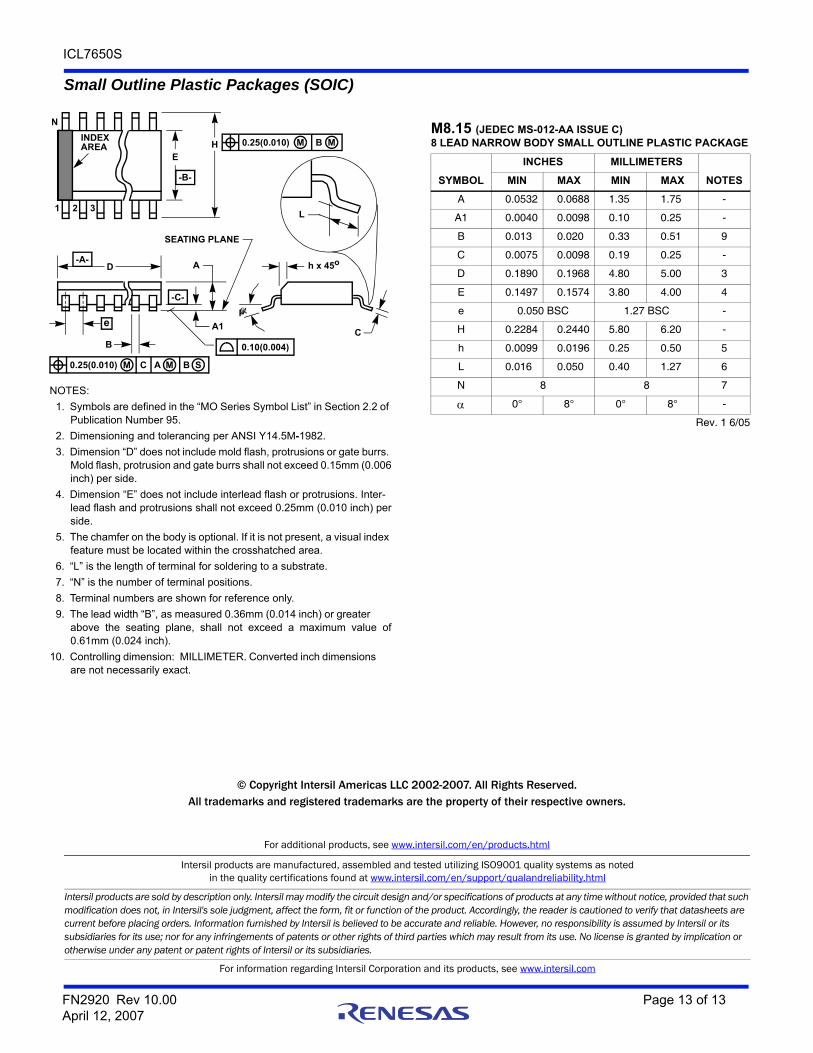
Small Outline Plastic Packages (SOIC)
INDEXAREA
E
D
N
1 2 3
-B-
0.25(0.010) C AM B S
e
-A-
L
B
M
-C-
A1
A
SEATING PLANE
0.10(0.004)
h x 45o
C
H
µ
0.25(0.010) BM M
NOTES:
1. Symbols are defined in the “MO Series Symbol List” in Section 2.2 of Publication Number 95.
2. Dimensioning and tolerancing per ANSI Y14.5M-1982.
3. Dimension “D” does not include mold flash, protrusions or gate burrs. Mold flash, protrusion and gate burrs shall not exceed 0.15mm (0.006inch) per side.
4. Dimension “E” does not include interlead flash or protrusions. Inter-lead flash and protrusions shall not exceed 0.25mm (0.010 inch) perside.
5. The chamfer on the body is optional. If it is not present, a visual index feature must be located within the crosshatched area.
6. “L” is the length of terminal for soldering to a substrate.
7. “N” is the number of terminal positions.
8. Terminal numbers are shown for reference only.
9. The lead width “B”, as measured 0.36mm (0.014 inch) or greater above the seating plane, shall not exceed a maximum value of0.61mm (0.024 inch).
10. Controlling dimension: MILLIMETER. Converted inch dimensions are not necessarily exact.
M8.15 (JEDEC MS-012-AA ISSUE C)8 LEAD NARROW BODY SMALL OUTLINE PLASTIC PACKAGE
SYMBOL
INCHES MILLIMETERS
NOTESMIN MAX MIN MAX
A 0.0532 0.0688 1.35 1.75 -
A1 0.0040 0.0098 0.10 0.25 -
B 0.013 0.020 0.33 0.51 9
C 0.0075 0.0098 0.19 0.25 -
D 0.1890 0.1968 4.80 5.00 3
E 0.1497 0.1574 3.80 4.00 4
e 0.050 BSC 1.27 BSC -
H 0.2284 0.2440 5.80 6.20 -
h 0.0099 0.0196 0.25 0.50 5
L 0.016 0.050 0.40 1.27 6
N 8 8 7
0° 8° 0° 8° -
Rev. 1 6/05