Embed Size (px)
Citation preview

1
Features
• CMOS Design for Very Low Power
• Output Drivers Directly Drive Both Digits andSegments of Large 8-Digit LED Displays
• Measures Frequencies from DC to 10MHz; Periodsfrom 0.5µs to 10s
• Stable High Frequency Oscillator uses either 1MHz or10MHz Crystal
• Both Common Anode and Common Cathode Available
• Control Signals Available for External SystemsInterfacing
• Multiplexed BCD Outputs
Applications• Frequency Counter
• Period Counter
• Unit Counter
• Frequency Ratio Counter
• Time Interval Counter
Description
The ICM7226 is a fully integrated Universal Counter andLED display driver. It combines a high frequency oscillator, adecade timebase counter, an 8-decade data counter andlatches, a 7-segment decoder, digit multiplexer and segmentand digit drivers which can directly drive large LED displays.The counter inputs accept a maximum frequency of 10MHzin frequency and unit counter modes and 2MHz in the othermodes. Both inputs are digital inputs. In many applications,amplification and level shifting will be required to obtainproper digital signals for these inputs.
The ICM7226 can function as a frequency counter, periodcounter, frequency ratio (fA/fB) counter, time interval counteror as a totalizing counter. The devices require either a10MHz or 1MHz quartz crystal timebase, or if desired anexternal timebase can also be used. For period and timeinterval, the 10MHz timebase gives a 0.1µs resolution. Inperiod average and time interval average, the resolution canbe in the nanosecond range. In the frequency mode, theuser can select accumulation times of 0.01s, 0.1s, 1s and10s. With a 10s accumulation time, the frequency can bedisplayed to a resolution of 0.1Hz. There is 0.2s betweenmeasurements in all ranges. Control signals are provided toenable gating and storing of prescaler data.
Leading zero blanking has been incorporated with frequencydisplay in kHz and time in µs. The display is multiplexed at a500Hz rate with a 12.2% duty cycle for each digit. TheICM7226A is designed for common anode displays with typi-cal peak segment currents of 25mA, and the ICM7226B isdesigned for common cathode displays with typical segmentcurrents of 12mA. In the display off mode, both digit driversand segment drivers are turned off, allowing the display tobe used for other functions.
Part Number Information
PART NUMBERTEMP.
RANGE (oC) PACKAGEPKG.NO.
ICM7226AlJL -25× to 85 40 Ld CERDIP F40.6
ICM7226BlPL -25× to 85 40 Ld PDIP E40.6
May 2001
ICM7226A,ICM7226B
8-Digit, Multi-Function,Frequency Counter/Timer
File Number 3169.2CAUTION: These devices are sensitive to electrostatic discharge; follow proper IC Handling Procedures.1-888-INTERSIL or 321-724-7143 | Intersil and Design is a trademark of Intersil Americas Inc. | Copyright © Intersil Americas Inc. 2001
itleM7
6A,M72B)b-t (8-git,lti-
nc-n,-
encyunteime
utho)ey-rdster-
rpo-ion,mi-n-ctor-
encyunteime
git,tru-nta-n,wwer,ta
OBSOLETE PRODUCT
POSSIBLE SUBSTITUTE PRODUCT
ICM7216

PinoutsICM7226A
COMMON ANODE (CERDIP)TOP VIEW
ICM7226BCOMMON CATHODE (PDIP)
TOP VIEW
NOTE:
1. For maximum frequency stability, connect to VDD or VSS.
CONTROL INPUT
INPUT B
FUNCTION
SEG e
SEG g
SEG a
VSS
SEG d
SEG b
SEG c
SEG f
RST INPUT
EXT DP IN
INPUT A
BUF OSC OUT
OSC OUT
EXT RANGE
D1
D3
D5
VDD
D6
D7
D8
HOLD
D2
D4
STORE
13
1
2
3
4
5
6
7
8
9
10
11
12
14
15
16
17
18
19
20
28
40
39
38
37
36
35
34
33
32
31
30
29
27
26
25
24
23
22
21 RANGE
OSC IN
NC (NOTE 1)
NC (NOTE 1)
EXT OSC IN
RST OUT
MEASUREMENT IN PROGRESS
BCD 2
BCD 1
BCD 4
BCD 8
DP
CONTROL INPUT
INPUT B
FUNCTION
D3
D2
D4
VSS
D5
D6
D7
D8
RST INPUT
EXT DP IN
INPUT A
BUF OSC OUT
OSC OUT
EXT RANGE
DP OUT
SEG e
SEG d
VDD
SEG b
SEG c
SEG f
HOLD
SEG g
SEG a
STORE
13
1
2
3
4
5
6
7
8
9
10
11
12
14
15
16
17
18
19
20
28
40
39
38
37
36
35
34
33
32
31
30
29
27
26
25
24
23
22
21 RANGE
OSC IN
NC (NOTE 1)
NC (NOTE 1)
EXT OSC IN
RST OUT
MEASUREMENT IN PROGRESS
BCD 2
BCD 1
BCD 4
BCD 8
D1
ICM7226A, ICM7226B
2

Functional Block Diagram
STOREAND RESET
REFERENCE
DIGITDECODER
OSC 104 OR
RANGE
CONTROL
DP
DECODERSEGMENT
INPUT
INPUT
FN
MAIN
DRIVERS
COUNTER+103
LOGIC
FF
CONTROLLOGIC
CONTROLLOGIC
CONTROLLOGIC
DATA LATCHES
OUTPUT MUX
MAIN
÷103
SELECT
CONTROLLOGIC
LOGIC
DRIVERSAND LZB
FUNCTIONINPUT
D
CL
EN
CLOVERFLOW
STORE
100Hz
Q
HOLDINPUT
INPUT B
SEGMENTOUTPUTS
EXTDP
INPUT
CONTROLINPUT
DIGITOUTPUTS
(8)
(8)
3
8 8
5
6
4 7 8
6
4 4 4 4 4 4 4 4
LOGIC
RANGESELECTLOGIC105
EXT RANGEINPUT
LOGIC
4 4
MEAS INPROGRESS
OUTPUT
RANGEINPUTEXT OSC
INPUT
OSCINPUT
BUF OSCOUTPUT
RESETINPUT
INPUT A
OSCOUTPUT
COUNTERRESET
BCDOUTPUTS
(4)
RESETOUTPUT
STOREOUTPUT
8
R
ICM7226A, ICM7226B
3

Absolute Maximum Ratings Thermal Information
Maximum Supply Voltage (VDD - VSS). . . . . . . . . . . . . . . . . . . . 6.5VMaximum Digit Output Current . . . . . . . . . . . . . . . . . . . . . . . . 400mAMaximum Segment Output Current . . . . . . . . . . . . . . . . . . . . . 60mAVoltage On Any Input orOutput Terminal (Note 1) . . . . . . . . . . . . . . VDD +0.3V to VSS -0.3V
Operating ConditionsTemperature Range . . . . . . . . . . . . . . . . . . . . . . . . . . -25oC to 85oC
Thermal Resistance (Typical, Note 2) θJA (oC/W) θJC (oC/W)CERDIP Package . . . . . . . . . . . . . . . . 45 9PDIP Package . . . . . . . . . . . . . . . . . . . 50 N/A
Maximum Junction TemperatureCERDIP Package . . . . . . . . . . . . . . . . . . . . . . . . . . . . . . . . 175oCPDIP Package . . . . . . . . . . . . . . . . . . . . . . . . . . . . . . . . . . . 150oC
Maximum Storage Temperature Range . . . . . . . . . . -55oC to 150oCMaximum Lead Temperature (Soldering 10s) . . . . . . . . . . . . . 300oC
CAUTION: Stresses above those listed in “Absolute Maximum Ratings” may cause permanent damage to the device. This is a stress only rating and operationof the device at these or any other conditions above those indicated in the operational sections of this specification is not implied.
NOTES:
1. Destructive latchup may occur if input signals are applied before the power supply is established or if inputs or outputs are forced tovoltages exceeding VDD or VSS by 0.3V.
2. θJA is measured with the component mounted on an evaluation PC board in free air.
Electrical Specifications VDD = 5.0V, TA = 25oC, Unless Otherwise Specified
PARAMETER TEST CONDITIONS MIN TYP MAX UNITS
Operating Supply Current, IDD Display Off, Unused Inputs to VSS - 2 5 mA
Supply Voltage Range (VDD -VSS), VSUPPLY -25oC to 85oC, INPUT A,INPUT B Frequency at fMAX
4.75 - 6.0 V
Maximum Frequency INPUT A, Pin 40, fA(MAX) -25oC to 85oC4.75V < VDD < 6.0V, Figure 9Function = Frequency, Ratio,Unit Counter
10 14 - MHz
Function = Period, Time Interval 2.5 - - MHz
Maximum Frequency INPUT B, Pin 2, fB(MAX) -25oC to 85oC4.75V < VDD < 6.0V, Figure 10
2.5 - - MHz
Minimum Separation INPUT A to INPUT B,Time Interval Function
-25oC to 85oC4.75V < VDD < 6.0V, Figure 1
250 - - ns
Oscillator Frequency and External Oscillator Frequency,fOSC
-25oC to 85oC4.75V < VDD < 6.0V
0.1 - 10 MHz
Oscillator Transconductance, gM VDD -4.75V, TA = 85oC 2000 - - µS
Multiplex Frequency, fMUX fOSC = 10MHz - 500 - Hz
Time Between Measurements fOSC = 10MHz - 200 - ms
Input Rate of Charge, dVIN/dt Inputs A, B - 15 - mV/µs
Input Voltages: Pins 2, 19, 33, 39, 40, 35
Input Low Voltage, VIL -25oC to 85oC - - 1.0 V
Input High Voltage, VlH 3.5 - - V
Pins 2, 39, 40, Input Leakage, A, B, IILK - - 20 µA
Input Resistance to VDD Pins 19, 33, RIN VIN = VDD -1.0V 100 400 - kΩ
Input Resistance to VSS Pin 31, RIN VIN = +1.0V 50 100 - kΩ
Output Current
Low Output Current, Pins 3, 5-7, 17, 18, 32, 38, IOL VOL = +0.4V 400 - - µA
High Output Current, Pins 5-7, 17, 18, 32, HOL VOH = +2.4V 100 - - µA
High Output Current, Pins 3, 38, HOL VOH = VDD -0.8V 265 - - µA
ICM7226A
Segment Driver: Pins 8-11, 13-16
Low Output Current, IOL VO = +1.5V 25 35 - mA
High Output Current, IOH VO = VDD -1.0V - 100 - µA
ICM7226A, ICM7226B
4

Timing Waveform
Multiplex Inputs: Pins 1, 4, 20, 21
Input Low Voltage, VIL - - 0.8 V
Input High Voltage, VIH 2.0 - - V
Input Resistance to VSS, RIN VIN = +1.0V 50 100 - kΩ
Digit Driver: Pins 22-24, 26-30
Low Output Current, IOL VO = +1.0V - -0.3 - mA
High Output Current, IOH VO = VDD -2.0V 150 180 - mA
ICM7226B
Segment Driver: Pins 22-24, 26-30
Leakage Current, IL VO = VSS - - 10 µA
High Output Current, IOH VO = VDD -2.0V 10 15 - mA
Multiplex Inputs: Pins 1, 4, 20, 21
Input Low Voltage, VIL - - VDD-2.0 V
Input High Voltage, VIH VDD-0.8 - - V
Input Resistance to VSS, RIN VIN = VDD -1.0V 100 360 - kΩ
Digit Driver: Pins 8-11, 13-16
Low Output Current, IOL VO = +1.0V 50 75 - mA
High Output Current, IOH VO = VDD -2.5V - 100 - µA
NOTES:
1. Assumes all leads soldered or welded to PC board and free air flow.
2. Typical values are not tested.
Electrical Specifications VDD = 5.0V, TA = 25oC, Unless Otherwise Specified (Continued)
PARAMETER TEST CONDITIONS MIN TYP MAX UNITS
MEASUREMENTIN PROGRESS
30ms TO 40ms
STORE
RESET
INPUT A
INPUT B
PRIMING EDGES
PRIMING
FUNCTION:TIME INTERVAL
UPDATE190ms TO 200ms
40ms
60ms
40ms
MEASUREMENT INTERVAL
250ns MINMEASUREDINTERVAL
(FIRST)MEASUREDINTERVAL
(LAST)
UPDATE
NOTE:
1. If range is set to 1 event, first and last measured interval will coincide.
FIGURE 1. WAVEFORMS FOR TIME INTERVAL MEASUREMENT (OTHERS ARE SIMILAR, BUT WITHOUT PRIMING PHASE)
ICM7226A, ICM7226B
5

Typical Performance Curves
FIGURE 2. ICM7226B TYPICAL IDIGIT vs VOUT FIGURE 3. ICM7226A TYPICAL IDIG vs VDD-VOUT
FIGURE 4. ICM7226B TYPICAL ISEG vs VDD-VOUT FIGURE 5. ICM7226A TYPICAL ISEG vs VOUT
FIGURE 6. ICM7226B TYPICAL IDIGIT vs VOUT FIGURE 7. ICM7226A TYPICAL ISEG vs VOUT
VDD = 5.5V
200
50
100
00 1 2 3
VOUT (V)
I DIG
IT(m
A)
50
TA = 25oC
VDD = 4.5VVDD = 5.0V
85oC
-20oC
4.5 ≤ VDD ≤ 6.0V300
200
100
00 1 2 3
VDD-VOUT (V)
I DIG
(mA
)
25oC
85oC
-20oC4.5 ≤ VDD ≤ 6.0V30
20
10
00 1 2 3
VDD-VOUT (V)
I SE
G(m
A)
25oC
VDD = 5.5V
80
60
40
00 1 2 3
VOUT (V)
I SE
G(m
A)
20
TA = 25oC
VDD = 4.5V
VDD = 5.0V
85oC
-20oCVDD = 5.0V200
150
100
00 1 2 3
VOUT (V)
I DIG
IT(m
A)
25oC
50
85oC
-20oCVDD = 5.0V
80
60
40
00 1 2 3
VOUT (V)
I SE
G(m
A)
25oC
20
ICM7226A, ICM7226B
6
7
Description
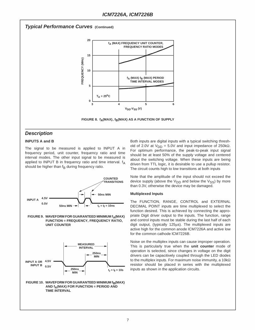
INPUTS A and B
The signal to be measured is applied to INPUT A infrequency period, unit counter, frequency ratio and timeinterval modes. The other input signal to be measured isapplied to INPUT B in frequency ratio and time interval. fAshould be higher than fB during frequency ratio.
Both inputs are digital inputs with a typical switching thresh-old of 2.0V at VDD = 5.0V and input impedance of 250kΩ.For optimum performance, the peak-to-peak input signalshould be at least 50% of the supply voltage and centeredabout the switching voltage. When these inputs are beingdriven from TTL logic, it is desirable to use a pullup resistor.The circuit counts high to low transitions at both inputs
Note that the amplitude of the input should not exceed thedevice supply (above the VDD and below the VSS) by morethan 0.3V, otherwise the device may be damaged.
Multiplexed Inputs
The FUNCTION, RANGE, CONTROL and EXTERNALDECIMAL POINT inputs are time multiplexed to select thefunction desired. This is achieved by connecting the appro-priate Digit driver output to the inputs. The function, rangeand control inputs must be stable during the last half of eachdigit output, (typically 125µs). The multiplexed inputs areactive high for the common anode lCM7226A and active lowfor the common cathode lCM7226B.
Noise on the multiplex inputs can cause improper operation.This is particularly true when the unit counter mode ofoperation is selected, since changes in voltage on the digitdrivers can be capacitively coupled through the LED diodesto the multiplex inputs. For maximum noise immunity, a 10kΩresistor should be placed in series with the multiplexedinputs as shown in the application circuits.
FIGURE 8. fA(MAX), fB(MAX) AS A FUNCTION OF SUPPLY
Typical Performance Curves (Continued)
fA (MAX) FREQUENCY UNIT COUNTER,FREQUENCY RATIO MODES
fA (MAX) fB (MAX) PERIODTIME INTERVAL MODES
TA = 25oC
VDD-VSS (V)
FR
EQ
UE
NC
Y(M
Hz)
20
15
10
5
03 4 5 6
INPUT A 4.5V
0.5V50ns MIN tr = tf = 10ns
COUNTEDTRANSITIONS
50ns MIN
FIGURE 9. WAVEFORM FOR GUARANTEED MINIMUM fA(MAX)FUNCTION = FREQUENCY, FREQUENCY RATIO,UNIT COUNTER
INPUT A ORINPUT B
4.5V
0.5V
MEASUREDINTERVAL
250nsMIN
tr = tf = 10s250nsMIN
FIGURE 10. WAVEFORM FOR GUARANTEED MINIMUM fB(MAX)AND fA(MAX) FOR FUNCTION = PERIOD ANDTIME INTERVAL
ICM7226A, ICM7226B

Table 1 shows the functions selected by each digit for theseinputs.
Function Input
The six functions that can be selected are: Frequency,Period, Time Interval, Unit Counter, Frequency Ratio andOscillator Frequency.
The implementation of different functions is done by routingthe different signals to two counters, called “Main Counter”and “Reference Counter”. A simplified block diagram of thedevice for functions realization is shown in Figure 11. Table 2shows which signals will be routed to each counter in differ-ent cases. The output of the Main Counter is the informationwhich goes to the display. The Reference Counter divides itsinput to 1, 10, 100 and 1000. One of these outputs will beselected through the range selector and drive the enableinput of the Main Counter. This means that the ReferenceCounter, along with its' associated blocks, directs the MainCounter to begin counting and determines the length of thecounting period. Note that Figure 11 does not show the com-plete functional diagram (See the Functional Block Dia-gram). After the end of each counting period, the output ofthe Main Counter will be latched and displayed, then thecounter will be reset and a new measurement cycle willbegin. Any change in the FUNCTION INPUT will stop thepresent measurement without updating the display and theninitiate a new measurement. This prevents an erroneous firstreading after the FUNCTION INPUT is changed. In allcases, the 1-0 transitions are counted or timed.
TABLE 1. MULTIPLEXED INPUT FUNCTIONS
INPUT FUNCTION DIGIT
FUNCTION INPUTPin 4
Frequency D1
Period D8
Frequency Ratio D2
Time Interval D5
Unit Counter D4
Oscillator Frequency D3
RANGE INPUTPin 21
0.01s/1 Cycle D1
0.1s/10 Cycles D2
1s/100 Cycles D3
10s/1K Cycles D4
Enable External Range Input D5
CONTROL INPUTPin 1
Display Off D4 andHold
Display Test D8
1MHz Select D2
External Oscillator Enable D1
External Decimal PointEnable
D3
External DP INPUTPin 20
Decimal point is output for same digitthat is connected to this input.
TABLE 2. INPUT ROUTING
FUNCTIONMAIN
COUNTER COUNTER
Frequency (fA) Input A 100Hz (Oscillator ³÷105 or 104)
Period (tA) Oscillator Input A
Ratio (fA/fB) Input A Input B
Time Interval(A→B)
Oscillator Input AInput B
Unit Counter(Count A)
Input A Not Applicable
Osc. Freq.(fOSC)
Oscillator 100Hz (Oscillator ³÷105 or 104)
INTERNAL CONTROL
100Hz
INPUT A
INPUT B
INPUTSELECTOR
INTERNAL OREXTERNAL
OSCILLATOR
INPUT A
ENABLE
CLOCK
MAIN COUNTER
RANGE SELECTOR
÷1 ÷10 ÷100 ÷1000
INTERNAL CONTROL
INTERNAL CONTROL
CLOCK
INTERNAL CONTROL
INPUTSELECTOR
REFERENCE COUNTER
FIGURE 11. SIMPLIFIED BLOCK DIAGRAM OF FUNCTIONS IMPLEMENTATION
ICM7226A, ICM7226B
8

9
Frequency - In this mode input A is counted by the MainCounter for a precise period of time. This time is determinedby the time base oscillator and the selected range. For the10MHz (or 1MHz) time base, the resolutions are 100Hz,10Hz, 1Hz and 0.1Hz. The decimal point on the display isset for kHz reading.
Period - In this mode, the timebase oscillator is counted bythe Main Counter for the duration of 1, 10, 100 or 1000(range selected) periods of the signal at input A. A 10MHztimebase gives resolutions of 0.1µs to 0.0001µs for 1000periods averaging. Note that the maximum input frequencyfor period measurement is 2.5MHz.
Frequency Ratio - In this mode, the input A is counted bythe Main Counter for the duration of 1, 10, 100 or 1000(range selected) periods of the signal at input B. The fre-quency at input A should be higher than input B for meaning-ful result. The result in this case is unitless and its resolutioncan go up to 3 digits after decimal point.
Time Interval - In this mode, the timebase oscillator is countedby the Main Counter for the duration of a 1-0 transition of inputA until a 1-0 transition of input B. This means input A starts thecounting and input B stops it. If other ranges, except 0.01s/1cycle are selected the sequence of input A and B transitionsmust happen 10, 100 or 1000 times until the display becomesupdated; note this when measuring long time intervals to giveenough time for measurement completion. The resolution inthis mode is the same as for period measurement. See theTime Interval Measurement section also.
Unit Counter - In this mode, the Main Counter is alwaysenabled. The input A is counted by the Main Counter anddisplayed continuously.
Oscillator Frequency - In this mode, the device makes afrequency measurement on its timebase. This is a self testmode for device functionality check. For 10MHz timebasethe display will show 10000.0, 10000.00, 10000.000 andOverflow in different ranges.
Range Input
The RANGE INPUT selects whether the measurement period ismade for 1,10,100 or 1000 counts of the Reference Counter or itis controlled by EXT RANGE input. As it is shown in Table 1, thisgives different counting windows for frequency measurementand various cycles for other modes of measurement.
In all functional modes except Unit Counter, any change inthe RANGE INPUT will stop the present measurement with-out updating the display and then initiate a new measure-ment. This prevents an erroneous first reading after theRANGE INPUT is changed.
Control Input
Unlike the other multiplexed inputs, to which only one of thedigit outputs can be connected at a time, this input can betied to different digit lines to select combination of controls.In this case, isolation diodes must be used in digit lines toavoid crosstalk between them (see Figure 19). The directionof diodes depends on the device version, common anode orcommon cathode. For maximum noise immunity at this input,in addition to the 10K resistor which was mentioned before,
a 39pF to 100pF capacitor should also be placed betweenthis input and the VDD or VSS (See Figure 19).
Display Off - To disable the display drivers, it is necessary to tiethe D4 line to the CONTROL INPUT and have the HOLD inputat VDD. While in Display Off mode, the segments and digit driv-ers are all off, leaving the display lines floating, so the displaycan be shared with other devices. In this mode, the oscillatorcontinues to run with a typical supply current of 1.5mA with a10MHz crystal, but no measurements are made and multi-plexed inputs are inactive. A new measurement cycle will be ini-tiated when the HOLD input is switched to VSS.
Display Test - Display will turn on with all the digits showing8s and all decimal points also on. The display will be blankedif Display Off is selected at the same time.
1MHz Select - The 1MHz select mode allows use of a 1MHzcrystal with the same digit multiplex rate and time betweenmeasurement as with a 10MHz crystal. This is done by divid-ing the oscillator frequency by 104 rather than 105. The dec-imal point is also shifted one digit to the right in period andtime interval, since the least significant digit will be in µsincrement rather than 0.1µs increment.
External Oscillator Enable - In this mode, the signal at EXTOSC INPUT is used as a timebase instead of the on-boardcrystal oscillator (built around the OSC INPUT, OSC OUTPUTinputs). This input can be used for an external stable tempera-ture compensated crystal oscillator or for special measure-ments with any external source. The on-board crystal oscillatorcontinues to work when the external oscillator is selected. Thisis necessary to avoid hang-up problems, and has no effect onthe chip's functional operation. If the on-board oscillator fre-quency is less than 1MHz or only the external oscillator is used,THE OSC INPUT MUST BE CONNECTED TO THE EXT OSCINPUT providing the timebase has enough voltage swing forOSC INPUT (See Electrical Specifications). If the external time-base is TTL level a pullup resistor must be used for OSCINPUT. The other way is to put a 22MΩ resistor between OSCINPUT and OSC OUTPUT and capacitively couple the EXTOSC INPUT to OSC INPUT. This will bias the OSC INPUT atits threshold and the drive voltage will need to be only 2VP-P.The external timebase frequency must be greater than 100kHzor the chip will reset itself to enable the on-board oscillator.
External Decimal Point Enable - In this mode, the EX DPINPUT is enabled. A decimal point will be displayed for thedigit that its output line is connected to this input (EX DPINPUT). Digit 8 should not be used since it will override theoverflow output. Leading zero blanking is effective for thedigits to the left of selected decimal point.
Hold Input
Except in the unit counter mode, when the HOLD input isat VDD, any measurement in progress (before STORE goeslow) is stopped, the main counter is reset and the chip isheld ready to initiate a new measurement as soon as HOLDgoes low. The latches which hold the main counter data arenot updated, so the last complete measurement is displayed.In unit counter mode when HOLD input is at VDD, thecounter is not stopped or reset, but the display is frozen atthat instantaneous value. When HOLD goes low the countcontinues from the new value in the new counter.
ICM7226A, ICM7226B

RST IN Input
The RST IN is provided to reset the Main Counter, stop anymeasurement in progress, and enable the display latches,resulting in the all zero display. It is suggested to have acapacitor at this input to VSS to prevent any hangup problemon power up. See application circuits.
EXT RANGE Input
This input is provided to select ranges other than thoseprovided in the chip. In any mode of measurement the durationof measurement is determined by the EXT RANGE if this inputis enabled. This input is sampled at 10ms intervals by the100Hz reference derived from the timebase. Figure 12 showsthe relationship between this input, 100Hz reference signal andMEAS IN PROGRESS. EXT RANGE can change stateanywhere during the period of 100Hz reference by will besampled at the trailing edge of the period to start or stopmeasurement.
This input should not be used for short arbitrary ranges(because of its sampling period), it is provided for very longgating purposes. A way of using the ICM7226 for a shortarbitrary range is to feed the gating signal into the INPUT Band run the device in the Frequency Ratio mode. Note thatthe gating period will be from one positive edge until the nextpositive edge of INPUT B (0.01s/1 cycle range).
MEAS IN PROGRESS, STORE, RST OUT Outputs
These outputs are provided for external system interfacing.MEAS IN PROGRESS stays low during measurements andgoes high for intervals between measurements. Figure 13shows the relationship between these outputs for intervalsbetween measurements. All these outputs can drive a lowpower Schottky TTL. The MEAS IN PROGRESS can driveone ECL load if the ECL device is powered from the samepower supply as the ICM7226.
BCD Outputs
The BCD representation of each display digit is available atthe BCD outputs in a multiplexed fashion. See Table 3 for dig-its truth table. The BCD output of each digit is available whenits corresponding digit output is activated. Note that the digitoutputs are multiplexed from D8 (MSD) to D1 (LSD). The pos-itive going (ICM7226A, common anode) or the negative going(ICM7226B, common cathode) digit drive signals lag the BCDdata by 2µs to 6µs. This starting edge of each digit drive sig-nal should be used to externally latch the BCD data. EachBCD output drives one low power Schottky TTL load. Leadingzero blanking has no effect on the BCD outputs.
BUF OSC OUT Output
The BUFFered OSCillator OUTput is provided for use of theon-board oscillator signal, without loading the oscillator itself.This output can drive one low power Schottky TTL load. Careshould be taken to minimize capacitive loading on this pin.
Decimal Point Position
Table 4 shows the decimal point position for different modesof lCM7226 operation. Note that the digit 1 is the least signif-icant digit. Table is given for 10MHz timebase frequency.
REFERENCECOUNTER
CLOCK
MEASIN PROGRESS
EXT RANGEINPUT
tr
FIGURE 12. EXTERNAL RANGE INPUT TO END OFMEASUREMENT IN PROGRESS
TABLE 3. TRUTH TABLE BCD OUTPUTS
NUMBERBCD 8PIN 7
BCD 4PIN 6
BCD 2PIN 17
BCD 1PIN 18
0 0 0 0 0
1 0 0 0 1
2 0 0 1 0
3 0 0 1 1
4 0 1 0 0
5 0 1 0 1
6 0 1 1 0
7 0 1 1 1
8 1 0 0 0
9 1 0 0 1
40ms
STORE
RESET OUT
60ms30ms TO
40ms
40ms
190ms TO 200msMEAS
IN PROGRESS
FIGURE 13. RESET OUT, STORE AND MEASUREMENT INPROGRESS OUTPUTS BETWEEN MEASUREMENTS
TABLE 4. DECIMAL POINT POSITIONS
RANGE FREQUENCY PERIODFREQUENCY
RATIOTIME
INTERVALUNIT
COUNTEROSCILLATORFREQUENCY
0.01s/1 Cycle D2 D2 D1 D2 D1 D2
0.1s/10 Cycle D3 D3 D2 D3 D1 D3
1s/100 Cycle D4 D4 D3 D4 D1 D4
10s/1K Cycle D5 D5 D4 D5 D1 D5
External N/A N/A N/A N/A N/A N/A
ICM7226A, ICM7226B
10
11
Overflow Indication
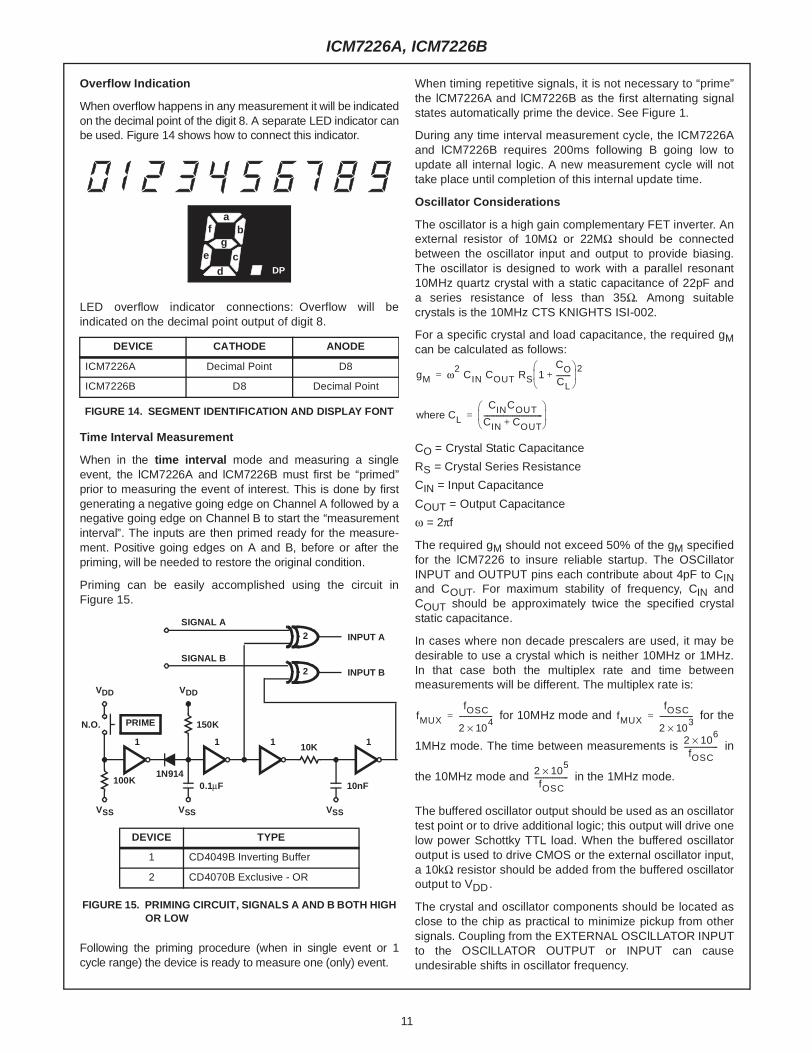
When overflow happens in any measurement it will be indicatedon the decimal point of the digit 8. A separate LED indicator canbe used. Figure 14 shows how to connect this indicator.
Time Interval Measurement
When in the time interval mode and measuring a singleevent, the lCM7226A and lCM7226B must first be “primed”prior to measuring the event of interest. This is done by firstgenerating a negative going edge on Channel A followed by anegative going edge on Channel B to start the “measurementinterval”. The inputs are then primed ready for the measure-ment. Positive going edges on A and B, before or after thepriming, will be needed to restore the original condition.
Priming can be easily accomplished using the circuit inFigure 15.
Following the priming procedure (when in single event or 1cycle range) the device is ready to measure one (only) event.
When timing repetitive signals, it is not necessary to “prime”the lCM7226A and lCM7226B as the first alternating signalstates automatically prime the device. See Figure 1.
During any time interval measurement cycle, the ICM7226Aand lCM7226B requires 200ms following B going low toupdate all internal logic. A new measurement cycle will nottake place until completion of this internal update time.
Oscillator Considerations
The oscillator is a high gain complementary FET inverter. Anexternal resistor of 10MΩ or 22MΩ should be connectedbetween the oscillator input and output to provide biasing.The oscillator is designed to work with a parallel resonant10MHz quartz crystal with a static capacitance of 22pF anda series resistance of less than 35Ω. Among suitablecrystals is the 10MHz CTS KNIGHTS ISI-002.
For a specific crystal and load capacitance, the required gMcan be calculated as follows:
CO = Crystal Static Capacitance
RS = Crystal Series Resistance
CIN = Input Capacitance
COUT = Output Capacitance
ω = 2πf
The required gM should not exceed 50% of the gM specifiedfor the lCM7226 to insure reliable startup. The OSCillatorINPUT and OUTPUT pins each contribute about 4pF to CINand COUT. For maximum stability of frequency, CIN andCOUT should be approximately twice the specified crystalstatic capacitance.
In cases where non decade prescalers are used, it may bedesirable to use a crystal which is neither 10MHz or 1MHz.In that case both the multiplex rate and time betweenmeasurements will be different. The multiplex rate is:
for 10MHz mode and for the
1MHz mode. The time between measurements is in
the 10MHz mode and in the 1MHz mode.
The buffered oscillator output should be used as an oscillatortest point or to drive additional logic; this output will drive onelow power Schottky TTL load. When the buffered oscillatoroutput is used to drive CMOS or the external oscillator input,a 10kΩ resistor should be added from the buffered oscillatoroutput to VDD.
The crystal and oscillator components should be located asclose to the chip as practical to minimize pickup from othersignals. Coupling from the EXTERNAL OSClLLATOR INPUTto the OSClLLATOR OUTPUT or INPUT can causeundesirable shifts in oscillator frequency.
ab
cd
fg
eDP
LED overflow indicator connections: Overflow will beindicated on the decimal point output of digit 8.
FIGURE 14. SEGMENT IDENTIFICATION AND DISPLAY FONT
DEVICE CATHODE ANODE
ICM7226A Decimal Point D8
ICM7226B D8 Decimal Point
SIGNAL A
SIGNAL B
INPUT A
INPUT B
VDD
N.O.
100K1N914
VDD
150K
1
0.1µF
10K
10nF
1 1 1
2
2
VSS VSS VSS
PRIME
FIGURE 15. PRIMING CIRCUIT, SIGNALS A AND B BOTH HIGHOR LOW
DEVICE TYPE
1 CD4049B Inverting Buffer
2 CD4070B Exclusive - OR
gM ω2CIN COUT RS 1
COCL--------+
2
=
where CL
CINCOUTCIN COUT+---------------------------------
=
fMUX
fOSC
2 104×
-------------------= fMUX
fOSC
2 103×
-------------------=
2 106×
fOSC-------------------
2 105×
fOSC-------------------
ICM7226A, ICM7226B
Display Considerations
The display is multiplexed at a 500Hz rate with a digit time of244µs. An interdigit blanking time of 6µs is used to preventdisplay ghosting (faint display of data from previous digitsuperimposed on the next digit). Leading zero blanking isprovided, which blanks the left hand zeroes after decimalpoint or any non zero digits. Digits to the right of the decimalpoint are always displayed. The leading zero blanking will bedisabled when the Main Counter overflows.
The lCM7226A is designed to drive common anode LED dis-plays at peak current of 25mA/segment, using displays withVF = 1.8V at 25mA. The average DC current will be greaterthan 3mA under these conditions. The lCM7226B is designedto drive common cathode displays at peak current of15mA/segment using displays with VF = 1.8V at 15mA. Resis-tors can be added in series with the segment drivers to limitthe display current, if required. The Typical PerformanceCurves show the digit and segment currents as a function ofoutput voltage for common anode and common cathodedrivers.
To increase the light output from the displays, VDD may beincreased to 6.0V. However, care should be taken to see thatmaximum power and current ratings are not exceeded.
The SEGment and Digit outputs in both the ICM7226A andICM7226B are not directly compatible with either TTL or
CMOS logic. Therefore, level shifting with discrete transis-tors may be required to use these outputs as logic signals.External latching should be down on the leading edge of thedigit signal.
Accuracy
In a Universal Counter, crystal drift and quantization errorscause errors. In frequency, period and time intervalmodes, a signal derived from the oscillator is used in eitherthe Reference Counter or Main Counter, and in thesemodes, an error in the oscillator frequency will cause anidentical error in the measurement. For instance, an oscilla-tor temperature coefficient of 20ppm/oC will cause a mea-surement error of 20ppm/oC.
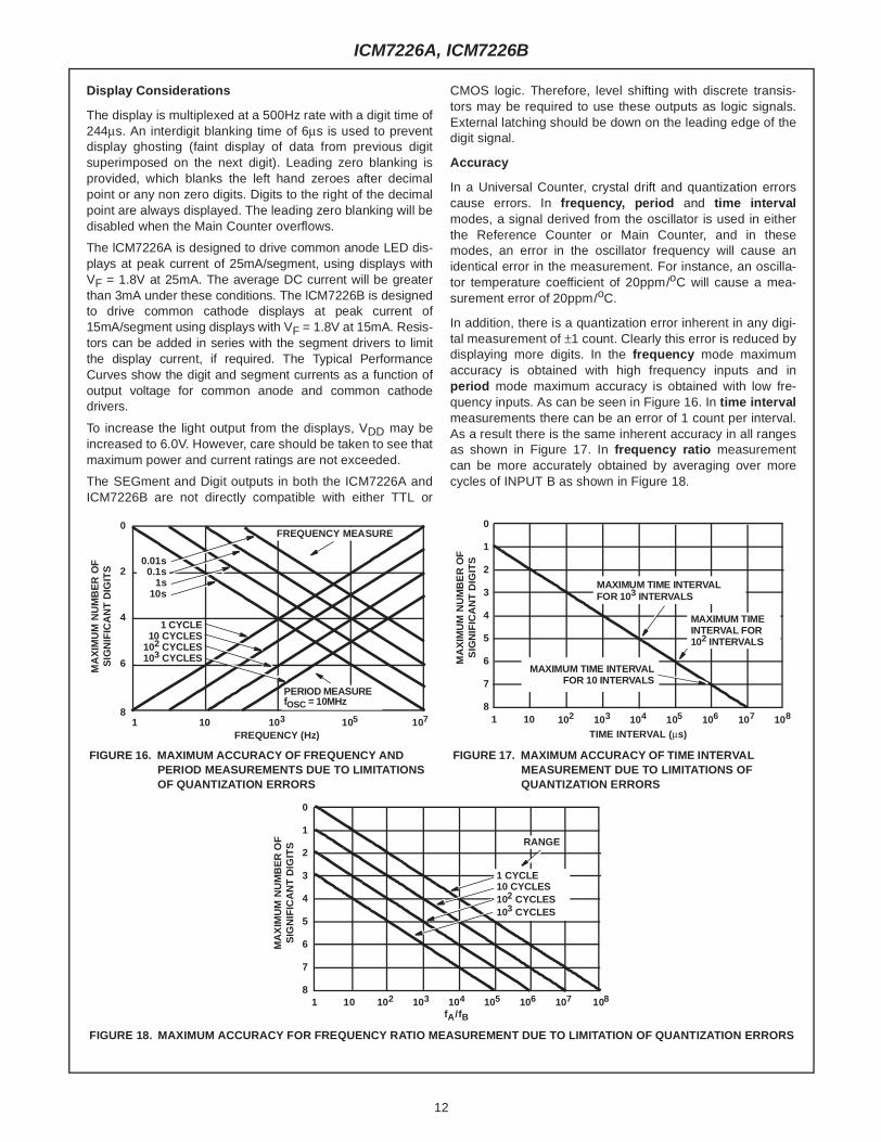
In addition, there is a quantization error inherent in any digi-tal measurement of ±1 count. Clearly this error is reduced bydisplaying more digits. In the frequency mode maximumaccuracy is obtained with high frequency inputs and inperiod mode maximum accuracy is obtained with low fre-quency inputs. As can be seen in Figure 16. In time intervalmeasurements there can be an error of 1 count per interval.As a result there is the same inherent accuracy in all rangesas shown in Figure 17. In frequency ratio measurementcan be more accurately obtained by averaging over morecycles of INPUT B as shown in Figure 18.
FIGURE 16. MAXIMUM ACCURACY OF FREQUENCY ANDPERIOD MEASUREMENTS DUE TO LIMITATIONSOF QUANTIZATION ERRORS
FIGURE 17. MAXIMUM ACCURACY OF TIME INTERVALMEASUREMENT DUE TO LIMITATIONS OFQUANTIZATION ERRORS
FIGURE 18. MAXIMUM ACCURACY FOR FREQUENCY RATIO MEASUREMENT DUE TO LIMITATION OF QUANTIZATION ERRORS
FREQUENCY MEASURE0
2
4
81 10 103 107
FREQUENCY (Hz)
MA
XIM
UM
NU
MB
ER
OF
6
0.01s
SIG
NIF
ICA
NT
DIG
ITS
105
0.1s
10s1s
PERIOD MEASUREfOSC = 10MHz
1 CYCLE10 CYCLES
103 CYCLES102 CYCLES
MAXIMUM TIME INTERVALFOR 103 INTERVALS
MAXIMUM TIMEINTERVAL FOR102 INTERVALS
MAXIMUM TIME INTERVALFOR 10 INTERVALS
103 104 105 106 107 108102101
0
1
2
3
4
5
6
7
8
TIME INTERVAL (µs)
MA
XIM
UM
NU
MB
ER
OF
SIG
NIF
ICA
NT
DIG
ITS
1 CYCLE10 CYCLES
103 CYCLES102 CYCLES
RANGE
103 104 105 106 107 108102101
0
1
2
3
4
5
6
7
8
MA
XIM
UM
NU
MB
ER
OF
SIG
NIF
ICA
NT
DIG
ITS
fA/fB
ICM7226A, ICM7226B
12

13
Test Circuit
CONTROL INPUT
BUF OSC OUT
EXT RANGE
HOLD
13
1
2
3
4
5
6
7
8
9
10
11
12
14
15
16
17
18
19
20
28
40
39
38
37
36
35
34
33
32
31
30
29
27
26
25
24
23
22
21
EXT OSC IN
RST OUT
MEAS IN PROGRESS
39pF
INPUT B
FUNCTIONGENERATOR
FUNCTION INPUT A
GENERATOR
10K
DP
D1
D2
D3
D4
D8
D5 eg
a
d
b
c
f
FUNCTIONSTORE
BCD C
BCD D
BCD B
BCD A
RESET
abcdefgDP
OVERFLOWD8
D8 D7 D6 D5 D4 D3 D2 D1
8
86
6DENOTES BUSWITH 6
VDD = 5.0V
FUNCTIONGENERATOR
VSS
10kΩ
VDD
VDD
VDD22MΩ
10MHzCRYSTAL
VDD
30pF 39pF
VDDD1
D2
D3
D4
D5
D6
D7
D8
VDD
8
D1D2
D3
D5
8
100kΩD4
5
D8
D7
D6
D4
D1
D2D3
D5
100kΩ
DISPLAYTEST 1MHz
EXT
TESTDP
D8 D2 D1 D3
1N914s
DISPLAYOFF
D4
EXTOSC
D5
CONDUCTORS
CRYSTAL SPECS. =
FOCORS
10.00MHz22pF35Ω
ICM7226A
6
FIGURE 19.
DEVICE CATHODE ANODE
ICM7226A DP D8
ICM7226B D8 DP
NOTE: Overflow will be indicated on the decimal point output of digit 8.
ICM7226A, ICM7226B

Typical Applications
The ICM7226 has been designed as a complete stand aloneUniversal Counter, or used with prescalers and other circuitryin a variety of applications. Since INPUT A and INPUT B aredigital inputs, additional circuitry will be required in manyapplications, for input buffering, amplification, hysteresis, andlevel shifting to obtain the required digital voltages. For manyapplications a FET source follower can be used for input buff-ering, and an ECL 10116 line receiver can be used for amplifi-cation and hysteresis to obtain high impedance input,sensitivity and bandwidth. However, cost and complexity ofthis circuitry can vary widely, depending upon the sensitivityand bandwidth required. When TTL prescalers or input buffersare used, a pull up resistors to VDD should be used to obtainoptimal voltage swing at INPUTS A and B. If prescalers aren’trequired, the ICM7226 can be used to implement a minimumcomponent Universal Counter as shown in Figure 20.
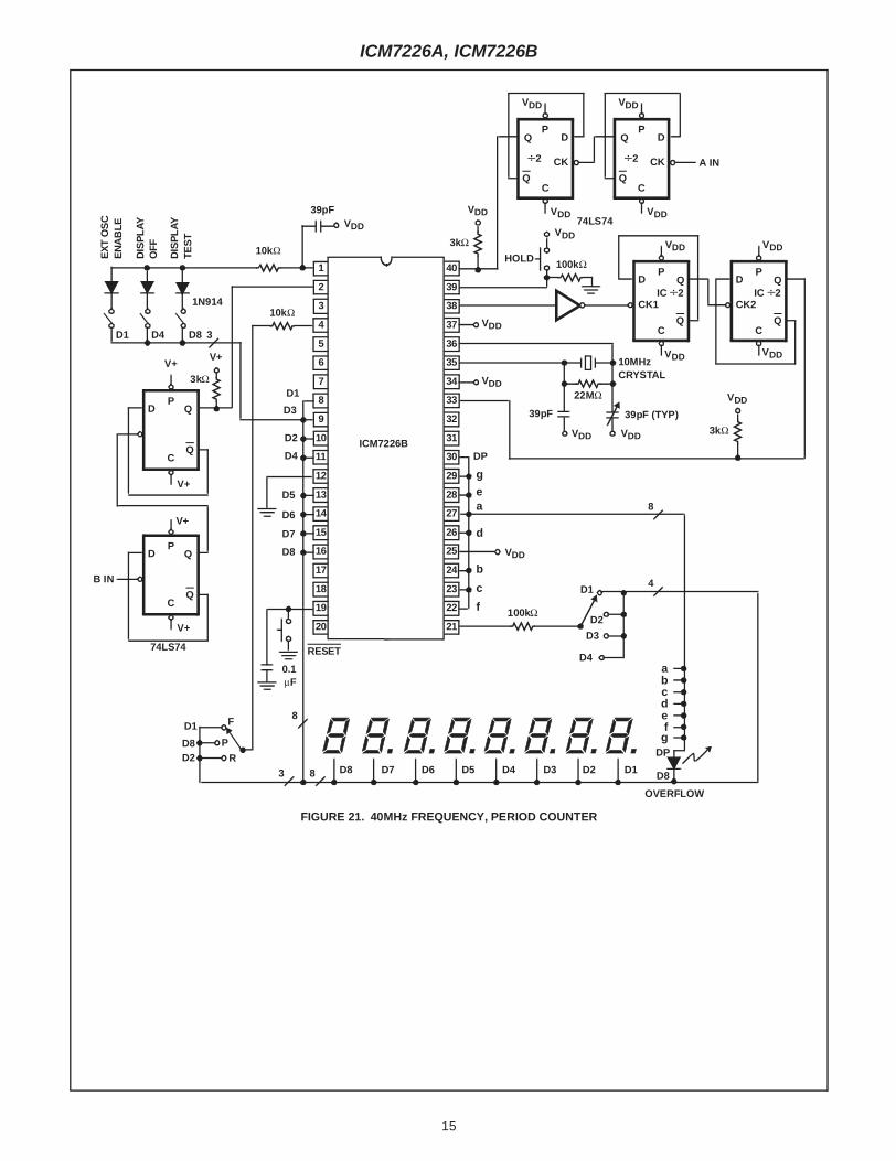
For input frequencies up to 40MHz, the circuit shown inFigure 21 can be used to implement a frequency andperiod counter. To obtain the correct value when measuringfrequency and period, it is necessary to divide the 10MHzoscillator frequency down to 2.5MHz. In doing this the timebetween measurements is lengthened to 800ms and the dis-play multiplex rate is decreased to 125Hz.
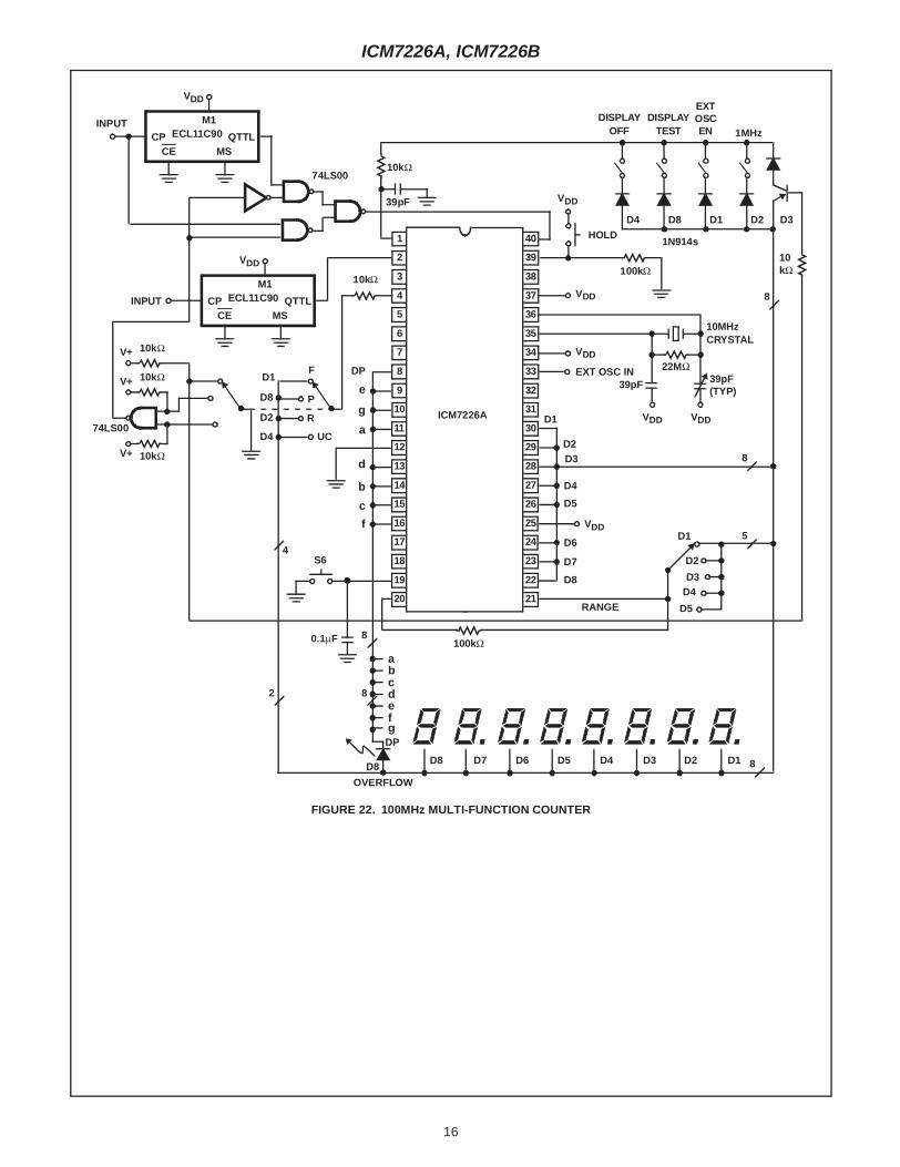
If the input frequency is prescaled by ten, the oscillatorfrequency can remain at either 10MHz or 1MHz, but thedecimal point must be moved. Figure 22 shows use of a ÷10prescaler in frequency counter mode. Additional logic hasbeen added to enable the ICM7226 to count the inputdirectly in period mode for maximum accuracy.
D8
HOLD
13
1
2
3
4
5
6
7
8
9
10
11
12
14
15
16
17
18
19
20
28
40
39
38
37
36
35
34
33
32
31
30
29
27
26
25
24
23
22
21
EXT OSC IN
39pF
10kΩ
D3
D1
D2
D3
D4
D8
D5
g
e
ad
b
c
f
RESET
D8 D7 D6 D5 D4 D3 D2 D1
86
VDD
100kΩ
V+
V+22MΩ
10MHzCRYSTAL
V+
39pF 39pF (TYP)
V+DP
D2
D5
D6
D7
D8 VDD
D1
D2
D3
100kΩ
D4
4
DISPLAYTEST
D8 D1
1N914s
DISPLAYBLANK
D4
TYPICAL
CLRS
22pF35Ω
abcdefgDP
0.1µF
ICM7226BD4
B IN
A IN
VDD
10kΩ
8
CRYSTALPARAMETERS
EXT OSCENABLE
3
FIGURE 20. 10MHz UNIVERSAL COUNTER
OVERFLOW
ICM7226A, ICM7226B
14
15
D8
HOLD
13
1
2
3
4
5
6
7
8
9
10
11
12
14
15
16
17
18
19
20
28
40
39
38
37
36
35
34
33
32
31
30
29
27
26
25
24
23
22
21
39pF
10kΩ
D3
gea
d
b
c
f
RESET
D8 D7 D6 D5 D4 D3 D2 D1
8
VDD
3kΩ
VDD
VDD22MΩ
10MHzCRYSTAL
VDD
39pF 39pF (TYP)
VDD
DP
D2
D5
D6
D7
D8 VDD
D1
D2
D3
100kΩ
D4
4
DIS
PL
AYO
FF
D4 D8
1N914
DIS
PL
AYTE
ST
D1
abcdefg
DP
0.1
ICM7226BD4
VDD
8
EX
TO
SC
EN
AB
LE
3
10kΩ
D1
µF
83
D Q
QC
P
V+
V+
B IN
D Q
QC
P
V+
V+V+
3kΩ
D1
D8D2
F
R
P
74LS74
DQ
QC
P
VDD
VDD
A IN
74LS74
CK
D Q
QC
P
VDD
VDD
CK1IC ÷2
VDD
100kΩ
DQ
QC
P
VDD
VDD
CK
D Q
QC
P
VDD
VDD
CK2IC ÷2
OVERFLOW
VDD
3kΩ
÷2 ÷2
FIGURE 21. 40MHz FREQUENCY, PERIOD COUNTER
ICM7226A, ICM7226B
D8
HOLD
13
1
2
3
4
5
6
7
8
9
10
11
12
14
15
16
17
18
19
20
28
40
39
38
37
36
35
34
33
32
31
30
29
27
26
25
24
23
22
21
EXT OSC IN
39pF
D3d
b
c
f
D8 D7 D6 D5 D4 D3 D2 D1
8
VDD
10
VDD
VDD22MΩ
10MHzCRYSTAL
VDD
39pF 39pF
VDD
D2
D5
D6
D7
D8
VDDD1
D2
D3
D5
5
DISPLAYTEST
D8 D2
1N914s
DISPLAYOFF
D4
abcdefgDP
0.1µF
ICM7226A
D4
10kΩ
EXT
8
8
100kΩ
D4RANGE
D1
8
OSCEN 1MHz
D1 D3
OVERFLOW
100kΩ
S6
(TYP)
kΩ10kΩ
8
4
QTTL
FV+ 10kΩ
V+ 10kΩ
MSCECP
M1
VDD
INPUT ECL11C90
QTTLMSCE
CP
M1
VDD
INPUTECL11C90
2
DP
a
g
eP
R
UC
D1
D8
D2
D4
V+ 10kΩ
74LS00
74LS00
FIGURE 22. 100MHz MULTI-FUNCTION COUNTER
ICM7226A, ICM7226B
16

17
D8
HOLD
13
1
2
3
4
5
6
7
8
9
10
11
12
14
15
16
17
18
19
20
28
40
39
38
37
36
35
34
33
32
31
30
29
27
26
25
24
23
22
21
39pF
10kΩ
D4
D1
D3
D8 D7 D6 D5 D4 D3 D2 D1
8
VDD
10kΩ
VDD
VDD22MΩ
10MHzCRYSTAL
VDD
39pF 39pF
VDD
VDD
DISPLAYTEST
D8
1N914s
DISPLAYOFF
D4
abcdefg
0.1µF
ICM7226B
10kΩ
3
10kΩ
8
D1
OVERFLOW
100kΩ
RESET
(TYP)
2N2222
10kΩ
2
D3
gea
d
b
c
f
DP
D2
D5
D6
D7
D8
D4
D1
D2
4
VDD
VDD
3kΩ
10kΩ
CONT 2
QTTLMSCE
CP
M1
VDD
INPUTECL11C90
VDD
VDD
FUNCTIONSWITCH
OPEN FREQCLOSEDPERIOD
F
OUTD1 IN
CD4016
CONT 2OUT
D8 IN
VDD
INPUT
N.O.
FIGURE 23. 100MHz FREQUENCY, PERIOD COUNTER
DP
ICM7226A, ICM7226B

Figure 23 shows the use of a CD4016 analog multiplexer tomultiplex the digital outputs back to the FUNCTION Input.Since the CD4016 is a digitally controlled analog transmissiongate, no level shifting of the digit output is required. CD4051sor CD4052s could also be used to select the proper inputs forthe multiplexed input on the ICM7226 from 2-bit or 3-bit digitalinputs. These analog multiplexers may also be used in sys-tems in which the mode of operation is controlled by a micro-processor rather than directly from front panel switches. TTLmultiplexers such as the 74LS153 or 74LS251 may also beused, but some additional circuitry will be required to convertthe digit output to TTL compatible logic levels.
The circuit shown in Figure 24 can be used in any of thecircuit applications shown to implement a single measure-ment mode of operation. This circuit uses the STORE output
to put the ICM7226 into a hold mode. The HOLD input canalso be used to reduce the time between measurements.The circuit shown in Figure 25 puts a short pulse into theHOLD input a short time after STORE goes low. A new mea-surement will be initiated at the end of the pulse on theHOLD input. This circuit reduces the time between measure-ments to about 40ms from 200ms; use of the circuit shown inFigure 25 on the circuit shown in Figure 21 will reduce thetime between measurements from 800ms to about 160ms.
Using LCD Display
Figure 26 shows the ICM7226 being interfaced to LCD dis-plays, by using its BCD outputs and 8 digit lines to drive twoICM7211 display drivers.
FIGURE 24. SINGLE MEASUREMENT CIRCUIT FOR USE WITHICM7226
FIGURE 25. CIRCUIT FOR REDUCING TIME BETWEENMEASUREMENTS
FIGURE 26. 10MHz UNIVERSAL COUNTER SYSTEM WITH LCD DISPLAY
VDD
100kΩ
STOREOUTPUT
S1
VDD
100kΩS2
VDD
100kΩS3
HOLDINPUT
SWITCH FUNCTION
S1 Open-Single Meas Mode Enabled
S2 Closed-Initiate New Measurement
S3 Closed-Hold Input
VDD
STOREOUTPUT HOLD
INPUT
100kΩ
100pF
100pF
HOLD SWITCH
100kΩ
N.O.
ICM7226A
ab
cd
fg
e
ab
cd
fg
e
ab
cd
fg
e
ab
cd
fg
e
ab
cd
fg
e
ab
cd
fg
e
ab
cd
fg
e
ab
cd
fg
e
ICM7211ICM7211
5
28 SEGMENT LINES 28 SEGMENT LINES
5
1+5V
35 31 32 33 34
22 23 24 26
30 29 28 27 30292827
181767
31 32 33 34
27 28 29 30
1+5V
3536
D8 • • D1D8 • • D5
ICM7226A, ICM7226B
18
19
All Intersil products are manufactured, assembled and tested utilizing ISO9000 quality systems.Intersil Corporation’s quality certifications can be viewed at website www.intersil.com/design/quality/iso.asp.
Intersil products are sold by description only. Intersil Corporation reserves the right to make changes in circuit design and/or specifications at any time without notice.Accordingly, the reader is cautioned to verify that data sheets are current before placing orders. Information furnished by Intersil is believed to be accurate and reli-able. However, no responsibility is assumed by Intersil or its subsidiaries for its use; nor for any infringements of patents or other rights of third parties which mayresult from its use. No license is granted by implication or otherwise under any patent or patent rights of Intersil or its subsidiaries.
For information regarding Intersil Corporation and its products, see web site www.intersil.com
Sales Office HeadquartersNORTH AMERICAIntersil Corporation2401 Palm Bay Rd.Palm Bay, FL 32905TEL: (321) 724-7000FAX: (321) 724-7240
EUROPEIntersil SAMercure Center100, Rue de la Fusee1130 Brussels, BelgiumTEL: (32) 2.724.2111FAX: (32) 2.724.22.05
ASIAIntersil Ltd.8F-2, 96, Sec. 1, Chien-kuo North,Taipei, Taiwan 104Republic of ChinaTEL: 886-2-2515-8508FAX: 886-2-2515-8369
ICM7226A, ICM7226B


![Interval Notation: ], not interval notationpgrant.weebly.com/uploads/2/3/2/7/23274454/6.3b_interval_notation.… · •Interval Notation: Uses different brackets to indicate an interval](https://img.pdfslide.net/doc/110x75/5f8344624904df613146ef90/interval-notation-not-interval-ainterval-notation-uses-different-brackets.jpg)