Embed Size (px)
Citation preview
ATWILC1000-MR110xB IEEE 80211 bgn Link Controller Module
Description
The ATWILC1000-MR110xB module is a low-power consumption IEEE 80211 bgn IoT (Internet ofThings) module which is specifically optimized for low power IoT applications This module features smallform factor (217mm x 147mm x 21mm) while fully integrating Power Amplifier (PA) Low Noise Amplifier(LNA) TransmitReceive (TR) switch power management and PCB antenna With advanced security itis interoperable with various vendors using IEEE 80211bgn Access Points in wireless LAN The moduleprovides Serial Peripheral Interface (SPI) and Secure Digital Input Output (SDIO) to interface with thehost controller
Note that all references to the ATWILC1000-MR110xB module include all the module devices listed belowunless otherwise noted
bull ATWILC1000-MR110PBbull ATWILC1000-MR110UB
Features
bull Compliant with IEEE 80211 bgn 20 MHz (1x1) solutionbull Supports Single spatial stream in 24 GHz ISM bandbull Integrated Power Amplifier (PA) and TransmitReceive (TR) switchbull Superior sensitivity and range through advanced PHY signal processingbull Advanced equalization and channel estimationbull Advanced carrier and timing synchronizationbull Wi-Fi Directreg and Soft-AP supportbull Supports IEEE 80211 WEP WPA WPA2 and WPA2-Enterprise securitybull Superior Medium Access Control (MAC) throughput through hardware accelerated two-level A-
MSDUA-MPDU frame aggregation and block acknowledgementbull On-chip memory management engine to reduce the host loadbull SPI and SDIO host interfacesbull Operating temperature ranges from -40degC to +85degCbull InputOutput operating voltage of 18V to 36Vbull Built-in 26 MHz crystalbull Power-save modes
ndash lt1microA Power-Down mode typical at 33V IOndash 380microA Doze mode with chip settings preserved (used for beacon monitoring)ndash On-chip low power Sleep oscillatorndash Fast host wake-up from Doze mode by a pin or the host IO transaction
bull Wi-Fi Alliancereg certified for connectivity and optimizations
copy 2017 Microchip Technology Inc Datasheet DS70005326B-page 1
ndash ID WFA65340
ATWILC1000-MR110xB
copy 2017 Microchip Technology Inc Datasheet DS70005326B-page 2
Table of Contents
Description1
Features 1
1 Ordering Information and Module Marking 5
2 Block Diagram 6
3 Pinout and Package Information 7
4 Electrical Specifications 1141 Absolute Ratings 1142 Recommended Operating Conditions 1143 Receiver Performance1144 Transmitter Performance1345 Timing Characteristics14
5 Power Management 1951 Current Consumption in Various Device States 1952 Restrictions for Power States2053 Power-UpDown Sequence2054 Digital IO Pin Behavior During Power-Up Sequences21
6 CPU and Memory Subsystems 2361 Processor 2362 Memory Subsystem2363 Nonvolatile Memory (eFuse) 23
7 WLAN Subsystem 2571 MAC 2572 PHY2673 Radio27
8 External Interfaces2881 Interfacing with the Host Microcontroller 2882 SPI Slave Interface2983 SDIO Slave Interface2984 UART Debug Interface 3085 I2C Slave Interface 31
9 Notes on Interfacing with the ATWILC1000-MR110xB 32
10 Application Reference Design 33
11 Module Outline Drawings 35
12 Design Consideration 38
copy 2017 Microchip Technology Inc Datasheet DS70005326B-page 3
121 ATWILC1000-MR110PB Placement and Routing Guidelines 38122 Printed PCB Antenna Performance of ATWILC1000-MR110PB39123 ATWILC1000-MR110UB Placement and Routing Guidelines 42
13 Reflow Profile Information 44131 Storage Condition44132 Solder Paste44133 Stencil Design 44134 Printing Process 44135 Baking Conditions 44136 Soldering and Reflow Condition45
14 Module Assembly Considerations 47
15 Regulatory Approval48151 United States48152 Canada50153 Europe51
16 Reference Documentation53
17 Document Revision History 54
The Microchip Web Site 57
Customer Change Notification Service57
Customer Support 57
Microchip Devices Code Protection Feature 57
Legal Notice58
Trademarks 58
Quality Management System Certified by DNV59
Worldwide Sales and Service60
ATWILC1000-MR110xB
copy 2017 Microchip Technology Inc Datasheet DS70005326B-page 4
1 Ordering Information and Module MarkingThe following table provides the ordering details of the ATWILC1000-MR110xB moduleTable 1-1 Ordering Details
Model Number Ordering Code Package No ofPins
Description RegulatoryCertification
ATWILC1000-MR110PB
ATWILC1000-MR110PB
217x147x21mm
28 Certified modulewith ATWILC1000B-MU chip and PCBantenna
FCC IC CE
ATWILC1000-MR110UB
ATWILC1000-MR110UB
217x147x21mm
28 Certified modulewith ATWILC1000B-MU chip and uFLconnector
FCC
The following figure provides the marking information of the ATWILC1000-MR110xB moduleFigure 1-1 Marking Information
ATWILC1000-MR110xB
copy 2017 Microchip Technology Inc Datasheet DS70005326B-page 5
2 Block DiagramThe following figure provides a basic overview of the ATWILC1000-MR110xB module
Figure 2-1 ATWILC1000-MR110xB Module Block Diagram
ATWILC1000-MR110xB
copy 2017 Microchip Technology Inc Datasheet DS70005326B-page 6
3 Pinout and Package InformationThe ATWILC1000-MR110xB package has an exposed paddle that must be connected to the systemboard ground The module pin assignment is shown in the following figure
Figure 3-1 Pin Assignment
Note This pin assignment is applicable for both ATWILC1000-MR110PB and ATWILC1000-MR110UBmodules
The following table describes the pin description of this module
Table 3-1 Pin Details
PinNo
Name Type Description ProgrammablePull up Resistor
1 GPIO_6 IO General purpose IO -
2 I2C_SCL IO I2C slave clock Used only for developmentdebug purposes It is recommended to addtest point for this pin
-
3 I2C_SDA IO I2C slave data Used only for developmentdebug purposes It is recommended to addtest point for this pin
Yes
4 RESET_N I Active-low hard reset When this pin isasserted low the module is placed in the
Yes
ATWILC1000-MR110xB
copy 2017 Microchip Technology Inc Datasheet DS70005326B-page 7
PinNo
Name Type Description ProgrammablePull up Resistor
reset state When this pin is asserted highthe module is out of reset and functionsnormally Connect to a host output thatdefaults low at power-up If the host outputis tri-stated add a 1 MΩ pull down resistorto ensure a low level at power-up
5 NC ndash No connection -
6 NC ndash No connection -
7 NC ndash No connection -
8 NC ndash No connection -
9 GND_1 Ground - -
10 SDIO_SPI_CFG I Connect to VDDIO through a 1MΩ resistorto enable the SPI interface Connect toground to enable SDIO interface
No
11 WAKE I Host wake control No
12 GND_2 Ground - -
13 IRQN O The ATWILC1000-MR110xB deviceinterrupt output Connect to a host interruptpin
No
14 SD_DAT3 SDIO=IO
UART=O
SDIO Data Line 3 from the ATWILC1000-MR110xB when module is configured forSDIO
Yes
15 SD_DAT2SPI_RXD
SDIO=IO
SPI=I
SDIO Data Line 2 signal fromATWILC1000-MR110xB when module isconfigured for SDIO SPI MOSI (MasterOut Slave In) pin when module isconfigured for SPI
Yes
16 SD_DAT1SPI_SSN
SDIO=IO
SPI=I
SDIO Data Line 1 from ATWILC1000-MR110xB when module is configured forSDIO Active low SPI slave select from theATWILC1000 when module is configuredfor SPI
Yes
17 SD_DAT0SPI_TXD
SDIO=IO
SPI=O
SDIO Data Line 0 from the ATWILC1000-MR110xB when module is configured forSDIO SPI MISO (Master In Slave Out) pinfrom ATWILC1000 when module isconfigured for SPI
Yes
18 SD_CMDSPI_CLK
SDIO=IO
SDIO CMD line from ATWILC1000-MR110xB when module is configured for
Yes
ATWILC1000-MR110xB
copy 2017 Microchip Technology Inc Datasheet DS70005326B-page 8
PinNo
Name Type Description ProgrammablePull up Resistor
SPI=I SDIO SPI Clock from ATWILC1000 whenmodule is configured for SPI
19 SD_CLK SDIO=I
UART=I
SDIO clock line for the ATWILC1000-MR110xB when module is configured forSDIO
Yes
20 VBATT Powersupply
Power supply pin for the DCDC convertor Yes
21 GPIO_1 IO General purpose IO Yes
22 CHIP_EN I Module enable High level enables modulelow level places module in power-downmode Connect to a host Output thatdefaults low at power-up If the host outputis tri-stated add a 1MΩ pull down resistor ifnecessary to ensure a low level at power-up
No
23 VDDIO Powersupply
IO power supply Must match host IOvoltage
-
24 1P3V_TP - 13V VDD Core Test Point Decouple with10uF and 001uF to GND
25 GPIO_3 IO General purpose IO By default UARTreceive input to ATWILC1000-MR110xBUsed only for development debugpurposes It is recommended to add testpoint for this pin
Yes
26 GPIO_4 IO General purpose IO Yes
27 GPIO_5 IO General purpose IO By default UARTtransmit output from ATWILC1000-MR110xB Used only for developmentdebug purposes It is recommended to addtest point for this pin
Yes
28 GND_3 Ground - -
29 Paddle Ground Exposed paddle GND This pad must besoldered to system ground
-
The following table provides the ATWILC1000-MR110xB module package dimensions
Table 3-2 ATWILC1000-MR110xB Module Package Information
Parameter Value Units
Package Size 2172 x 1473 mm
Pad Count 28 -
ATWILC1000-MR110xB
copy 2017 Microchip Technology Inc Datasheet DS70005326B-page 9
Parameter Value Units
Total Thickness 211 mm
Pad Pitch 1016
Pad Width 082
Exposed Pad size 37 x 37
ATWILC1000-MR110xB
copy 2017 Microchip Technology Inc Datasheet DS70005326B-page 10
4 Electrical Specifications
41 Absolute RatingsThe absolute maximum ratings for this module are listed in the following table
Table 4-1 ATWILC1000-MR110xB Module Absolute Maximum Ratings
Symbol Description Min Max Unit
VBATT Input supplyvoltage
-03 50 V
VDDIO IO voltage -03 50 V
Caution Stresses beyond those listed under Absolute Maximum Ratings cause permanentdamage to the device This is a stress rating only The functional operation of the device atthose or any other conditions above those indicated in the operation listings of this specificationis not implied Exposure to maximum rating conditions for extended periods affects the devicereliability
42 Recommended Operating ConditionsThe recommended operating conditions for this module is listed in the following table
Table 4-2 ATWILC1000-MR110xB Module Recommended Operating Conditions
Symbol Min Typ Max Unit
VBATT 30 33 42 V
VDDIO 18 33 36 V
Operatingtemperature
-40 +85 ordmC
Note 1 VBATT should be equal to or greater than VDDIO2 The voltage of VDDIO is dependent on system IO voltage3 Test Conditions -40ordmC to +85ordmC
43 Receiver PerformanceThe following are typical conditions for radio receiver performance
VBATT at 33 V VDDIO at 33V temperature at 25degC and WLAN Channel 6(2437 MHz)
The following table provides the receiver performance characteristics for this module
ATWILC1000-MR110xB
copy 2017 Microchip Technology Inc Datasheet DS70005326B-page 11
Table 4-3 Receiver Performance
Parameter Description Min Typ Max Unit
Frequency - 2412 - 2472 MHz
Sensitivity 80211b 1 Mbps DSSS - -94 -
dBm2 Mbps DSSS - -91 -
55 Mbps DSSS - -89 -
11 Mbps DSSS - -86 -
Sensitivity 80211g 6 Mbps OFDM - -88 -
dBm
9 Mbps OFDM - -87 -
12 Mbps OFDM - -86 -
18 Mbps OFDM - -84 -
24 Mbps OFDM - -82 -
36 Mbps OFDM - -78 -
48 Mbps OFDM - -74 -
54 Mbps OFDM - -73 -
Sensitivity 80211n (BW at 20 MHz) MCS 0 - -87 -
dBm
MCS 1 - -85 -
MCS 2 - -83 -
MCS 3 - -80 -
MCS 4 - -76 -
MCS 5 - -73 -
MCS 6 - -71 -
MCS 7 - -69 -
Maximum Receive Signal Level 1-11 Mbps DSSS 0 -
dBm6-54 Mbps OFDM -5 -
MCS 0 ndash 7 -5 -
Adjacent Channel Rejection 1 Mbps DSSS (30 MHz offset) - 50 -
dB
11 Mbps DSSS (25 MHz offset) - 43 -
6 Mbps OFDM (25 MHz offset) - 40 -
54 Mbps OFDM (25 MHz offset) - 25 -
MCS 0 ndash 20 MHz BW (25 MHz offset) - 40 -
MCS 7 ndash 20 MHz BW (25 MHz offset) - 20 -
Cellular Blocker Immunity 776-794 MHz CDMA - -14 -dBm
824-849 MHz GSM - -10 -
ATWILC1000-MR110xB
copy 2017 Microchip Technology Inc Datasheet DS70005326B-page 12
Parameter Description Min Typ Max Unit
880-915 MHz GSM - -10 -
1710-1785 MHz GSM - -15 -
1850-1910 MHz GSM - -15 -
1850-1910 MHz WCDMA - -24 -
1920-1980 MHz WCDMA - -24 -
44 Transmitter PerformanceThe following are typical conditions for radio transmitter performance
VBATT at 33 V VDDIO at 33V temperature at 25degC and WLAN Channel 6(2437 MHz)
The following table provides the transmitter performance characteristics for this module
Table 4-4 Transmitter Performance
Parameter Description Unit Minimum Typical Maximum
Frequency - MHz 2412 - 2472
Output Power1-2
ON_Transmit
80211b 1Mbps dBm - 176 -
80211b 11Mbps dBm - 182 -
80211g 6Mbps dBm - 187 -
80211g 54Mbps dBm - 167 -
80211n MCS 0 dBm - 173 -
80211n MCS 7 dBm - 138 -
Tx PowerAccuracy
- dB - plusmn152 -
CarrierSuppression
80211b mode dBc - -194 -
80211g mode dBc - -275 -
80211n mode dBc - -211 -
Out of BandTransmit Power
76-108 dBmHz - -125 -
776-794 dBmHz - -125 -
869-960 dBmHz - -125 -
925-960 dBmHz - -125 -
1570-1580 dBmHz - -125 -
1805-1880 dBmHz - -125 -
1930-1990 dBmHz - -125 -
2110-2170 dBmHz - -125 -
ATWILC1000-MR110xB
copy 2017 Microchip Technology Inc Datasheet DS70005326B-page 13
Parameter Description Unit Minimum Typical Maximum
HarmonicOutput Power4
2nd dBmMHz - -28 -
3rd dBmMHz - -33 -
4th dBmMHz - -40 -
5th dBmMHz - -28 -
Note 1 Measured at 80211 spec compliant EVMSpectral Mask2 Measured after RF matching network3 Operating temperature range is -40degC to +85degC RF performance is guaranteed at room
temperature of 25degC with a 2-3dB change at boundary conditions4 Measured at 11Mbps DG(Digital Gain)= -7 WLAN Channel 6 (2437 MHz)5 With respect to TX power different (higherlower) RF output power settings may be used for
specific antennas andor enclosures in which case recertification may be required6 The availability of some specific channels andor operational frequency bands are country
dependent and should be programmed at the Host product factory to match the intendeddestination Regulatory bodies prohibit exposing the settings to the end user This requirementneeds to be taken care of via Host implementation
45 Timing Characteristics
451 SPI TimingThe SPI slave interface supports four standard modes as determined by the Clock Polarity (CPOL) andClock Phase (CPHA) settings These modes are illustrated in the following table
Table 4-5 SPI Slave Modes
Mode CPOL CPHA
0 0 0
1 0 1
2 1 0
3 1 1
The red lines in the following figure correspond to clock phase at 0 and the blue lines correspond to clockphase at 1
ATWILC1000-MR110xB
copy 2017 Microchip Technology Inc Datasheet DS70005326B-page 14
Figure 4-1 SPI Slave Clock Polarity and Clock Phase Timing
z
z z
z
SCKCPOL = 0
CPOL = 1
SSN
RXDTXD(MOSIMISO)
CPHA = 0
CPHA = 1
2 3 4 5 6 7 8
1 2 3 4 5 6 7
1
8
The SPI timing is shown in the following figure
Figure 4-2 SPI Timing Diagram (SPI MODE CPOL=0 CPHA=0)
The SPI timing parameters are provided in the following table
Table 4-6 SPI Slave Timing Parameters1
Parameter Symbol Min Max Units
Clock Input Frequency2 fSCK - 48 MHz
Clock Low Pulse Width tWL 4 -ns
Clock High Pulse Width tWH 5 -
ATWILC1000-MR110xB
copy 2017 Microchip Technology Inc Datasheet DS70005326B-page 15
Parameter Symbol Min Max Units
Clock Rise Time tLH 0 7
Clock Fall Time tHL 0 7
TXD Output Delay3 tODLY 4 9 from SCK fall125 from SCKrise
RXD Input Setup Time tISU 1 -
RXD Input Hold Time tIHD 5 -
SSN Input Setup Time tSUSSN 3 -
SSN Input Hold Time tHDSSN 55 -
Note 1 Timing is applicable to all SPI modes2 Maximum clock frequency specified is limited by the SPI slave interface internal design actual
maximum clock frequency can be lower and depends on the specific PCB layout3 Timing is based on 15pF output loading
452 SDIO TimingThe SDIO Slave interface timing is shown in following figure
Figure 4-3 SDIO Timing Diagram
Slave timing parameters are provided in the following tableTable 4-7 SDIO Timing Parameters
Parameter Symbol Min Max Units
Clock InputFrequency1
fPP 0 50 MHz
Clock Low PulseWidth
tWL 9 - ns
ATWILC1000-MR110xB
copy 2017 Microchip Technology Inc Datasheet DS70005326B-page 16
Parameter Symbol Min Max Units
Clock High PulseWidth
tWH 45 -
Clock Rise Time tLH 0 5
Clock Fall Time tHL 0 5
Input Setup Time tISU 6 -
Input Hold Time tIH 4 -
Output Delay2 tODLY 3 11
1 Maximum clock frequency specified is limited by the SDIO Slave interface internal design actualmaximum clock frequency can be lower and depends on the specific PCB layout
2 Timing based on 15pF output loading
453 I2C TimingThe following figure illustrates I2C Slave timing
Figure 4-4 I2C Timing Diagram
The following table provides I2C Slave timing parameters
Table 4-8 I2C Timing Parameters
Parameter Symbol Min Max Units Remarks
SCL ClockFrequency
fSCL 0 400 kHZ -
SCL Low PulseWidth
tWL 13 - micros -
SCL High PulseWidth
tWH 06 - micros -
SCL SDA FallTime
tHL - 300 ns -
ATWILC1000-MR110xB
copy 2017 Microchip Technology Inc Datasheet DS70005326B-page 17
Parameter Symbol Min Max Units Remarks
SCL SDA RiseTime
tLH - 300 ns This is dictatedby externalcomponents
START SetupTime
tSUSTA 06 - micros -
START HoldTime
tHDSTA 06 - micros -
SDA SetupTime
tSUDAT 100 - ns -
SDA Hold Time tHDDAT 0 - ns Slave andMaster Default
MasterProgrammingOption
40 - ns
STOP Setuptime
tSUSTO 06 - micros -
Bus Free TimeBetween STOPand START
tBUF 13 - micros -
Glitch PulseReject
tPR 0 50 ns -
ATWILC1000-MR110xB
copy 2017 Microchip Technology Inc Datasheet DS70005326B-page 18
5 Power ManagementThe ATWILC1000-MR110xB module has several device states
bull On statesndash ON_Transmit ndash device actively transmits an 80211 signal Highest output power and nominal
current consumptionndash ON_Receive ndash device actively receivies an 80211 signal Lowest sensitivity and nominal
current consumptionndash ON_Doze ndash device is powered on but it does not actively transmit or receive the datandash Power_Down ndash device core supply is powered off
The following pins are used to switch between the ON and Power_Down statesbull CHIP_EN ndash this pin (pin 22) enables or disables the DCDC converterbull VDDIO ndash IO supply voltage from external supply
In the ON states VDDIO is ON and CHIP_EN is high (at VDDIO voltage level) To change from the ONstates to Power_Down state connect the RESETN and CHIP_EN pin to logic low (GND) by following thepower down sequence mentioned in Power-UpDown Sequence When VDDIO is off and CHIP_EN islow the chip is powered off with no leakage (also see Restrictions for Power States)
51 Current Consumption in Various Device StatesThe following table provides this modules current consumption in various device states
Table 5-1 Current Consumption
Device State Code Rate Output
Power (dBm)
Current Consumption1
IVBATT IVDDIO
ON_Transmit 80211b 1Mbps 176 266 mA 22 mA
80211b 11Mbps 185 239 mA 22 mA
80211g 6Mbps 186 249 mA 22 mA
80211g 54Mbps 169 173 mA 22 mA
80211n MCS 0 177 253 mA 22 mA
80211n MCS 7 140 164 mA 22 mA
ON_Receive 80211b 1Mbps NA 63 mA 22 mA
80211b 11Mbps NA 63 mA 22 mA
80211g 6Mbps NA 63 mA 22 mA
80211g 54Mbps NA 63 mA 22 mA
80211n MCS 0 NA 63 mA 22 mA
80211n MCS 7 NA 63 mA 22 mA
ATWILC1000-MR110xB
copy 2017 Microchip Technology Inc Datasheet DS70005326B-page 19
Device State Code Rate Output
Power (dBm)
Current Consumption1
ON_Doze NA NA 380microA lt10microA
Power_Down NA NA 125 uA(2)
Note 1 The power consumption values are measured when VBAT is 33V and VDDIO is 33V at 25degC2 Current consumption mentioned for these states is the sum of current consumed in VDDIO and
VBAT voltage rails
52 Restrictions for Power StatesWhen no power is supplied to the device the DCDC Converter output and VDDIO are both turned off (atground potential) In this case a voltage cannot be applied to the device pins because each pin containsan ESD diode from the pin to supply This diode will turn on when voltage higher than one diode-drop issupplied to the pin
If a voltage must be applied to the signal pads while the chip is in a low power state the VDDIO supplymust be on so the Sleep mode or power-down state must be used
Similarly to prevent the pin-to-ground diode from turning on do not apply a voltage that is more than onediode-drop below ground to any pin
53 Power-UpDown SequenceThe following figure illustrates the power-updown sequence for the ATWILC1000-MR110xB module
Figure 5-1 Power-UpDown Sequence
The following table provides power-updown sequence timing parameters
ATWILC1000-MR110xB
copy 2017 Microchip Technology Inc Datasheet DS70005326B-page 20
Table 5-2 Power-UpDown Sequence Timing
Parameter Min Max Units Description Notes
tA 0 - ms VBAT rise toVDDIO rise
VBAT and VDDIO can risesimultaneously or connected togetherVDDIO must not rise before VBAT
tB 0 - ms VDDIO rise toCHIP_EN rise
CHIP_EN must not rise before VDDIOCHIP_EN must be driven high or lowand must not be left floating
tC 5 - ms CHIP_EN rise toRESETN rise
This delay is required to stabilize the XOclock before RESETN removal RESETNmust be driven high or low and must notbe left floating
tArsquo 0 - ms VDDIO fall toVBAT fall
VBAT and VDDIO fall simultaneously orconnected together VBAT must not fallbefore VDDIO
tBrsquo 0 - ms CHIP_EN fall toVDDIO fall
VDDIO must not fall before CHIP_ENCHIP_EN and RESETN must fallsimultaneously
tCrsquo 0 - ms RESETN fall toVDDIO fall
VDDIO must not fall before RESETNRESETN and CHIP_EN fallsimultaneously
54 Digital IO Pin Behavior During Power-Up SequencesThe following table represents the digital IO pin states corresponding to the device power modes
Table 5-3 Digital IO Pin Behavior in Different Device States
Device State VDDIO CHIP_EN RESETN Output Driver InputDriver
Pull UpDownResistor (96
kOhm)
Power_Down coresupply OFF
High Low Low Disabled (Hi-Z) Disabled Disabled
Power-On Resetcore supply and hardreset ON
High High Low Disabled (Hi-Z) Disabled Enabled
Power-On Defaultcore supply ONdevice out of resetand not programmed
High High High Disabled (Hi-Z) Enabled Enabled
On_Doze
On_Transmit
High High High Programmedby firmware foreach pinenabled ordisabled
Oppositeof OutputDriverstate
Programmedby firmware foreach pinenabled ordisabled
ATWILC1000-MR110xB
copy 2017 Microchip Technology Inc Datasheet DS70005326B-page 21
Device State VDDIO CHIP_EN RESETN Output Driver InputDriver
Pull UpDownResistor (96
kOhm)
On_Receive coresupply ON deviceprogrammed byfirmware
ATWILC1000-MR110xB
copy 2017 Microchip Technology Inc Datasheet DS70005326B-page 22
6 CPU and Memory Subsystems
61 ProcessorThis ATWILC1000-MR110xB module has a Cortus APS3 32-bit processor This processor performs manyof the MAC functions including but not limited to association authentication power management securitykey management and MSDU aggregationdeaggregation In addition the processor provides flexibility forvarious modes of operation such as STA and AP modes
62 Memory SubsystemThe APS3 core uses a 128 KB instructionboot ROM along with a 160 KB instruction RAM and a 64 KBdata RAM In addition the device uses a 128 KB shared RAM accessible by the processor and MAC thatallows the APS3 core to perform various data management tasks on the Tx and Rx data packets
63 Nonvolatile Memory (eFuse)This ATWILC1000-MR110xB module has 768 bits of nonvolatile eFuse memory that is read by the CPUafter device reset This nonvolatile One-Time-Programmable (OTP) memory is used to store customerspecific parameters such as MAC address various calibration information such as Tx power crystalfrequency offset etc and other software-specific configuration parameters The eFuse is partitioned intosix 128 bit banks Each bank has the same bit map mentioned in the following figure The purpose of thefirst 80 bits in each bank is fixed and the remaining 48 bits are general purpose software dependent bitsEach bank is programmed independently which allows for several updates of the device parametersfollowing the initial programming For example if the MAC address has to be changed Bank 1 has to beprogrammed with the new MAC address along with the values of TX gain correction and Frequency offsetif they are used and programmed in the Bank 0 The contents of Bank 0 have to be invalidated in thiscase by programming the Invalid bit in the Bank 0 This will allow the firmware to use the MAC addressfrom Bank 1
By default all the ATWILC1000-MR110PB and ATWILC1000-MR110UB modules are programmed withthe MAC address and the Frequency offset bits of Bank 0
ATWILC1000-MR110xB
copy 2017 Microchip Technology Inc Datasheet DS70005326B-page 23
Figure 6-1 eFuse Bit Map
ATWILC1000-MR110xB
copy 2017 Microchip Technology Inc Datasheet DS70005326B-page 24
7 WLAN SubsystemThe WLAN subsystem is composed of the Media Access Controller (MAC) Physical Layer (PHY) andthe radio
71 MAC
711 DescriptionThis module is designed to operate at low power while providing high data throughput The IEEE 80211MAC functions are implemented with a combination of dedicated datapath engines hardwired controllogic and a low power high-efficiency microprocessor The combination of dedicated logic with aprogrammable processor provides optimal power efficiency and real time response while providing theflexibility to accommodate evolving standards and future feature enhancements
The dedicated datapath engines are used to implement data path functions with heavy computationalrequirements For example a Frame Check Sequence (FCS) engine checks the Cyclic RedundancyCheck (CRC) of the transmitting and receiving packets and a cipher engine performs all the requiredencryption and decryption operations for the WEP WPA-TKIP WPA2 CCMP-AES and WPA2 Enterprisesecurity requirements
Control functions which have real time requirements are implemented using hardwired control logicmodules These logic modules offer real time response while maintaining configurability through theprocessor Examples of hardwired control logic modules are the channel access control module(implements EDCAHCCA Beacon Tx control interframe spacing and so on) protocol timer module(responsible for the Network Access vector back-off timing timing synchronization function and slotmanagement) MAC Protocol Data Unit (MPDU) handling module aggregationdeaggregation moduleblock ACK controller (implements the protocol requirements for burst block communication) and TxRxcontrol Finite State Machine (FSM) (coordinate data movement between PHY and MAC interface cipherengine and the Direct Memory Acces (DMA) interface to the TxRx FIFOs)
Following are the characteristics of MAC functions implemented solely in software on the microprocessor
bull Functions with high memory requirements or complex data structures Examples are associationtable management and power save queuing
bull Functions with low computational load or without critical real time requirements Examples areauthentication and association
bull Functions that require flexibility and upgradeability Examples are beacon frame processing andQoS scheduling
712 FeaturesThe ATWILC1000-MR110xB IEEE 80211 MAC supports the following functions
bull IEEE 80211bgnbull IEEE 80211e WMM QoS EDCAPCF multiple access categories traffic schedulingbull Advanced IEEE 80211n features
ndash Transmission and reception of aggregated MPDUs (A-MPDU)ndash Transmission and reception of aggregated MSDUs (A-MSDU)ndash Immediate block acknowledgmentndash Reduced Interframe Spacing (RIFS)
bull Supports IEEE 80211i and WFA security with key management
ATWILC1000-MR110xB
copy 2017 Microchip Technology Inc Datasheet DS70005326B-page 25
ndash WEP 64128ndash WPA-TKIPndash 128-bit WPA2 CCMP (AES)ndash WPA2 Enterprise
bull Advanced power managementndash Standard IEEE 80211 Power save modendash Wi-Fi alliance WMM-PS (U-APSD)
bull RTS-CTS and CTS self supportbull Supports either STA or AP mode in the infrastructure basic service set modebull Supports concurrent mode of operationbull Supports Independent Basic Service Set (IBSS)
72 PHYThe ATWILC1000-MR110xB module WLAN PHY is designed to achieve reliable and power-efficientphysical layer communication specified by IEEE 80211 bgn in single stream mode with 20 MHzbandwidth The advanced algorithms are used to achieve maximum throughput in a real worldcommunication environment with impairments and interference The PHY implements all the requiredfunctions such as Fast Fourier Transform (FFT) filtering Forward Error Correction (FEC) that is a Viterbidecoder frequency timing acquisition and tracking channel estimation and equalization carrier sensingclear channel assessment and automatic gain control
Features
The IEEE 80211 PHY supports the following functions
bull Single antenna 1x1 stream in 20 MHz channelsbull Supports IEEE 80211b DSSS-CCK modulation 1 2 55 and 11 Mbpsbull Supports IEEE 80211g OFDM modulation 6 9 1218 24 36 48 and 54 Mbpsbull Supports IEEE 80211n HT modulations MCS0-7 20 MHz 800 and 400ns guard interval 65 72
130 144 195 217 260 289 390 433 520 578 585 650 and 722 Mbpsbull IEEE 80211n mixed mode operationbull Per packet Tx power controlbull Advanced channel estimationequalization automatic gain control CCA carriersymbol recovery
and frame detection
721 FeaturesThe IEEE 80211 PHY supports the following functions
bull Single antenna 1x1 stream in 20 MHz channelsbull Supports IEEE 80211b DSSS-CCK modulation 1 2 55 and 11 Mbpsbull Supports IEEE 80211g OFDM modulation 6 9 1218 24 36 48 and 54 Mbpsbull Supports IEEE 80211n HT modulations MCS0-7 20 MHz 800 and 400ns guard interval 65 72
130 144 195 217 260 289 390 433 520 578 585 650 and 722 Mbpsbull IEEE 80211n mixed mode operationbull Per packet Tx power controlbull Advanced channel estimationequalization automatic gain control CCA carriersymbol recovery
and frame detection
ATWILC1000-MR110xB
copy 2017 Microchip Technology Inc Datasheet DS70005326B-page 26
73 RadioThis section describes the properties and characteristics of the ATWILC1000- MR110xB and Wi-Fi radiotransmit and receive performance capabilities of the device The performance measurements are taken atthe RF pin assuming 50Ω impedance the RF performance is guaranteed for room temperature of 25degCwith a derating of 2-3dB at boundary conditions
Measurements were taken under typical conditions VBATT at 33V VDDIO at 33V and temperature at+25ordmC
Table 7-1 Features and Properties
Feature Description
Module Part Number ATWILC1000-MR110xB
WLAN Standard IEEE 80211bgn Wi-Fi compliant
Host Interface SPI SDIO
Dimension L x W x H 217 x 147 x 21 (typical) mm
Frequency range 2412 GHz ~ 2472 GHz (24 GHz ISM band)
Number of channels 11 for North America 13 for Europe
Modulation 80211b DQPSK DBPSK CCK
80211gn OFDM64-QAM16-QAM QPSK BPSK
Data rate 80211b 1 2 55 11 Mbps80211g 6 9 12 18 24 36 48 54 Mbps
Data rate
(20 MHz short GI400ns)
80211n 72 144 217 289 433 578 65722Mbps
Operating temperature(1) -40degC to 85degC
Storage temperature -40degC to 125degC
Humidity Operating humidity 10 to 95 non-condensing
Storage humidity 5 to 95 non-condensing
Note 1 RF performance is guaranteed at room temperature of 25degC with a 2-3db change at boundary
conditions
ATWILC1000-MR110xB
copy 2017 Microchip Technology Inc Datasheet DS70005326B-page 27
8 External InterfacesThis section describes the various host and debug interfaces of the ATWILC1000-MR110xB module
81 Interfacing with the Host MicrocontrollerThis section describes how to interface ATWILC1000-MR110xB module with the host microcontroller Theinterface comprises of a slave SPISDIO and additional control signals as shown in the figure Additionalcontrol signals are connected to the GPIOIRQ interface of the microcontroller
Figure 8-1 Interfacing with the Host Microcontroller
Table 8-1 Host Microcontroller Interface Pins
Module Pin Function(1)
4 RESET_N
11 WAKE
13 IRQ_N
22 CHIP_EN
16 SPI_SSNSD_DATA1
15 SPI_MOSISD_DATA2
17 SPI_MISOSD_DATA0
18 SPI_SCKSD_CMD
ATWILC1000-MR110xB
copy 2017 Microchip Technology Inc Datasheet DS70005326B-page 28
Module Pin Function(1)
14 SD_DATA3
19 SD_CLK
Note 1 Logic input for module pin SDIO_SPI_CFG(10) determines whether SDIO or SPI slave interface is
enabled Connect SDIO_SPI_CFG to VDDIO through a 1MΩ resistor to enable the SPI interfaceConnect SDIO_SPI_CFG to ground to enable SDIO interface
2 It is recommended to place test points for pins I2C_SDA(3) I2C_SCL(2) GPIO_3(25) andGPIO_5(27) in the design
82 SPI Slave InterfaceThe SPI slave interface can be enabled by connecting the SDIO_SPI_CFG pin to VDDIO This SPIinterface is used to exchange the control and 80211 data The SPI is a full duplex slave-synchronousserial interface that is available following reset when pin 10 (SDIO_SPI_CFG) is connected to VDDIO
The SPI interface pin mapping configuration is provided in the following table
Table 8-2 SPI Interface Pin Mapping
Pin SPI Function
10 SDIO_SPI_CFG Must be connected to VDDIO
16 SSN Active-Low Slave Select
15 MOSI Serial Data Receive
18 SCK Serial Clock
17 MISO Serial Data Transmit
When the SPI is not selected ie when SSN is high the SPI interface will not interfere with datatransfers between the serial master and other serial slave devices When the serial slave is not selectedits transmitted data output is buffered resulting in a high impedance drive onto the MISO line
The SPI interface responds to a protocol that allows an external host to read or write any register in thechip and also initiate DMA transfers
The SPI SSN MOSI MISO and SCK pins of this module have internal programmable pull up resistorsThese resistors are programmed to be disabled Otherwise if any of the SPI pins are driven to a low levelwhile this module is in the low power sleep state current will flow from the VDDIO supply through the pullup resistors increasing the current consumption of the module
83 SDIO Slave InterfaceThe SDIO interface is enabled by connecting the SDIO_SPI_CFG pin to ground This SDIO interface isused to exchange the control and 80211 data The SDIO interface is available after reset when pin 10(SDIO_SPI_CFG) is connected to ground
This SDIO is a full speed interface The interface supports the 1-bit4-bit SD transfer mode at the clockrange of 0-50 MHz The host uses this interface to read and write from any register within the chip andalso configures this module for DMA data transfer
ATWILC1000-MR110xB
copy 2017 Microchip Technology Inc Datasheet DS70005326B-page 29
The SDIO interface pin mapping configuration is provided in the following table
Table 8-3 ATWILC1000 SDIO Interface Pin Mapping
Pin SDIO Function
10 SDIO_SPI_CFG Must be connected to ground
14 DAT3 Data 3
15 DAT2 Data 2
16 DAT1 Data 1
17 DAT0 Data 0
18 CMD Command
19 CLK Clock
The SDIO card is detected when the it is inserted into an SDIO host During the normal initialization andinterrogation of the card by the host the card identifies itself as an SDIO device The host softwareobtains the card information in a tuple (linked list) format and determines if that cardrsquos IO function(s) areacceptable to activate If the card is acceptable it is allowed to power-up fully and start the IO function(s)built into the card
The SD memory card communication is based on an advanced 9-pin interface (clock command fourdata and three power lines) designed to operate at maximum operating frequency of 50 MHz
831 Featuresbull Compliant with SDIO card specification version 20bull Host clock rate variable between 0 and 50 MHzbull Supports 1-bit4-bit SD bus modesbull Allows card to interrupt hostbull Responds to direct readwrite (IO52) and extended readwrite (IO53) transactionsbull Supports suspendresume operation
84 UART Debug InterfaceThis module has a Universal Asynchronous ReceiverTransmitter (UART) interface on J25(RxD) andJ27(TxD) pins This interface should be used only for debugging purposes The UART is compatible withthe RS-232 standard where ATWILC1000-MR110xB operates as Data Terminal Equipment (DTE) It hasa two-pin RXDTXD interface
The default configuration for accessing the UART interface of ATWILC1000-MR110xB is mentionedbelow
bull Baud rate 115200bull Data 8 bitbull Parity Nonebull Stop bit 1 bitbull Flow control None
It also has Rx and Tx FIFOs which ensures reliable high speed reception and low software overheadtransmission FIFO size is 4x8 for both Rx and Tx direction The UART has status registers that show the
ATWILC1000-MR110xB
copy 2017 Microchip Technology Inc Datasheet DS70005326B-page 30
number of received characters available in the FIFO and various error conditions in addition it has theability to generate interrupts based on these status bits
An example of UART receiving or transmitting a single packet is shown in the following figure Thisexample shows 7-bit data (0x45) odd parity and two stop bits
Figure 8-2 Example of UART RX or TX Packet
85 I2C Slave InterfaceThis module provides an I2C bus slave that allows for easy debugging of the ATWILC1000-MR110xBdevices It supports I2C bus Version 21 ndash 2000
The I2C interface is used only for debug This interface is a two-wire serial interface consisting of a serialdata line (SDA Pin 17) and a serial clock (SCL Pin 18) It responds to seven bit address value 0x60This module I2C interface operates in standard mode (with data rates up to 100Kbs) and fast mode (withdata rates up to 400Kbs)
The I2C is a synchronous serial interface The SDA line is a bidirectional signal and changes only whenthe SCL line is low except for STOP START and RESTART conditions The output drivers are open-drain to perform wire AND functions on the bus The devices on the bus are limited to the 400pFcapacitance Data is transmitted in byte packages
For specific information refer to the Philips Specification entitled ldquoThe I2C -Bus Specification Version21rdquo
ATWILC1000-MR110xB
copy 2017 Microchip Technology Inc Datasheet DS70005326B-page 31
9 Notes on Interfacing with the ATWILC1000-MR110xBProgrammable Pull up Resistors
The ATWILC1000-MR110xB module provides programmable pull up resistors on various pins Thepurpose of these resistors is to keep any unused input pins from floating which causes excess current toflow through the input buffer from the VDDIO supply Any unused pin on the device must leave these pullup resistors enabled so that the pin will not float The default state at power-up is for the pull up resistorto be enabled however any pin that is used must have the pull up resistor disabled The reason for thisis that if any pins are driven to a low level while the device is in the low power sleep state current flowsfrom the VDDIO supply through the pull up resistors increasing the current consumption of the moduleSince the value of the pull up resistor is approximately 100 kOhm the current through any pull up resistorthat is being driven low is VDDIO100K For VDDIO = 33V the current is approximately 33 microA The pinsthat are used and have programmable the pull up resistor disabled should always be actively driven toeither a high or low level and not be allowed to float
ATWILC1000-MR110xB
copy 2017 Microchip Technology Inc Datasheet DS70005326B-page 32
10 Application Reference DesignThis section provides reference schematic for ATWILC1000-MR110xB module with SPI and SDIO hostinterfacesFigure 10-1 ATWILC1000-MR110xB Reference Schetmatic - SDIO Host Interface
Table 10-1 ATWILC1000-MR110xB reference Schematic - SDIO Host Interface - Bill of Materials
Item Qty Reference Value Description
Manufacturer
PartNumber
Footprint
1 9 R2 R3R4R5 R6R7 R8R9 R10
0 R RESISTORThick Film0 ohm0402
Yageo RC0402JR-070RL
0402
2 1 U1 ATWILC1000-MR110xB
Wi-FiModule
Microchip ATWILC1000-MR110xB
ATWILC1000-MR110xB
copy 2017 Microchip Technology Inc Datasheet DS70005326B-page 33
Figure 10-2 ATWILC1000-MR110xB Reference Schetmatic - SPI Host Interface
Table 10-2 ATWILC1000-MR110xB reference Schematic - SPI Host Interface - Bill of Materials
Item Qty Reference Value Description
Manufacturer
PartNumber
Footprint
1 1 R1 1 M RESISTORThick Film1 M ohm0402
Yageo RC0100FR-071ML
0402
2 9 R2 R3R4R5 R6R7 R8R9 R10
0 R RESISTORThick Film0 ohm0402
Yageo RC0402JR-070RL
0402
3 1 U1 ATWILC1000-MR110xB
Wi-FiModule
Microchip ATWILC1000-MR110xB
ATWILC1000-MR110xB
copy 2017 Microchip Technology Inc Datasheet DS70005326B-page 34
11 Module Outline DrawingsThe ATWILC1000-MR110PB module package details are outlined in the following figure Dimensions arein mm
Figure 11-1 Module Drawings ndash ATWILC1000-MR110PB - Top Bottom and Side Views
MODULE TOP VIEW
Metal Shield
Metal Shield
PCB
MODULE SIDE VIEW MODULE BOTTOM VIEW
NOTE THIS PAD MUST BE SOLDERED TO GND
NOT TO SCALE
The ATWILC1000-MR110UB module package details are outlined in the following figure Dimensions arein mm
ATWILC1000-MR110xB
copy 2017 Microchip Technology Inc Datasheet DS70005326B-page 35
Figure 11-2 Module Drawings ndash ATWILC1000-MR110UB - Top Bottom and Side Views
MODULE TOP VIEW
Metal Shield
Metal Shield
PCB
MODULE SIDE VIEW MODULE BOTTOM VIEW
NOTE THIS PAD MUST BE SOLDERED TO GND
NOT TO SCALE Rev 2
This section provides the outline drawing for the recommended footprint for the ATWILC1000-MR110xBmodule It is imperative that the center Ground Pad is provided with an array of GND vias to provide agood ground and act as thermal sink for the ATWILC1000-MR110xB module
ATWILC1000-MR110xB
copy 2017 Microchip Technology Inc Datasheet DS70005326B-page 36
Figure 11-3 Recommended Solder Pad Footprint
NOTE THIS PAD MUST BE TIED TO GND
1016 Pitch
1473
19
08
1016 Pitch
4064
267
267
600
1016 Pitch
370
370
1016 Pitch
19 3048
368
2172 2032
442
SOLDER PAD FOOTPRINT
Drawing not to scaleUntoleranced dimensionsUnits=mm
ATWILC1000-MR110xB
copy 2017 Microchip Technology Inc Datasheet DS70005326B-page 37
12 Design ConsiderationThis section provides the guidelines on placement and routing to achieve the best performance
121 ATWILC1000-MR110PB Placement and Routing GuidelinesIt is critical to follow the recommendations listed below to achieve the best RF performance
bull The module must be placed on host board The printed antenna area must overlap with the carrierboard The portion of the module containing the antenna should not stick out over the edge of thehost board The antenna is designed to work properly when it is sitting directly on top of a 15mmthick printed circuit board Figure 12-2 shows the best poor and worst case module placements inhost board
bull If the module is placed at the edge of the host board a minimum 22mm by 5 mm area directlyunder the antenna must be clear of all metal on all layers of the board ldquoIn-landrdquo placement isacceptable however deepness of keep-out area must grove to module edge to host board edgeplus 5 mmNote Do not place the module in the middle of the host board or far away from the host boardedge
bull Follow the module placement keepout host PCB cutout recommendation as shown in Figure 12-1ndash Avoid routing any traces in the highlighted region on the top layer of the host board which will
be directly below the module areandash Follow the electrical keepout layer recommendation as shown in Figure 12-1 There should be
no copper in all layers of the host board in this region Avoid placing any components (likemechanical spacers bumpon etc) in the recommended electrical keepout area
ndash Place GND polygon pour below the module with the recommended boundary in the top layerof the host board as shown in Figure 12-1 Do not have any breaks in this GND plane
ndash Place sufficient GND vias in the highlighted area below the module for better RFperformance
ndash It is recommended to have a 3x3 grid of GND vias solidly connecting the exposed GNDpaddle of the module to the inner layer ground plane This will act as a good ground andthermal conduction for the ATWILC1000-MR110PB module The GND vias should have aminimum via hole size of 03mm
ndash Follow the mechanical boundary of the host PCB as shown in the Figure 12-1bull Keep the large metal objects away from antenna to avoid electromagnetic field blockingbull Do not enclose the antenna within a metal shieldbull Keep any components which may radiate noise or signals within the 24 GHz ndash 25 GHz frequency
band away from the antenna and if possible shield those components Any noise radiated from thehost board in this frequency band will degrade the sensitivity of the module
bull Make sure the width of the traces routed to GND VDDIO and VBAT rails are sufficiently larger forhandling the peak Tx current consumption
ATWILC1000-MR110xB
copy 2017 Microchip Technology Inc Datasheet DS70005326B-page 38
Figure 12-1 ATWILC1000-MR110PB Placement Reference
Figure 12-2 ATWILC1000-MR110PB Placement Example
122 Printed PCB Antenna Performance of ATWILC1000-MR110PBThe printed PCB antenna on the ATWILC1000-MR110PB is a meandered Inverted F Antenna (IFA) Theantenna is fed via matching network which is matched for the module installed on 15mm thick mainboard Main board thickness deviation by plusmn1mm changes RXTX performance by plusmn1dB maximumreferring to RXTX performance with default antenna matching network and installed on 15mm thick mainboard
Measured antenna gain is -03dBi
ATWILC1000-MR110xB
copy 2017 Microchip Technology Inc Datasheet DS70005326B-page 39
Antenna Radiation PatternFollowing figures illustrate the antenna radiation pattern During the measurement the printed antenna isplaced in the XZ plane with Y axis being perpendicular to the module and pointing to the back of themoduleFigure 12-3 Antenna Radiation Pattern when Phi = 0 degree
Figure 12-4 Antenna Radiation Pattern when Phi = 90 degree
ATWILC1000-MR110xB
copy 2017 Microchip Technology Inc Datasheet DS70005326B-page 40
Figure 12-5 Antenna Radiation Pattern when Theta = 90 degree
ATWILC1000-MR110xB
copy 2017 Microchip Technology Inc Datasheet DS70005326B-page 41
123 ATWILC1000-MR110UB Placement and Routing GuidelinesThe ATWILC1000-MR110UB module has an Ultra Small Miniature RF Connector (uFL) for the externalantenna
The choice of antenna is limited to the antenna types for which the module was tested and approved Fora list of tested and approved antennas that may be used with the module refer to the respective countryin the Regulatory Approval section
An approved and tested antenna type is shown in the following Table
Table 12-1 Tested External Antenna Type
Antenna Type Gain
PCB Antenna 20 dBi
ATWILC1000-MR110xB
copy 2017 Microchip Technology Inc Datasheet DS70005326B-page 42
1231 Recommended External Antenna for ATWILC1000-MR110UBPCB Antenna (Part number W3525B039) along with a 10cm length RF cable assembly (uFL to SMA)has been used for the certification of ATWILC1000-MR110UB It is recommended to use the same orsimilar external antenna in design
ATWILC1000-MR110xB
copy 2017 Microchip Technology Inc Datasheet DS70005326B-page 43
13 Reflow Profile InformationThis section provides the guidelines for the reflow process to get the module soldered to the customersdesign
131 Storage Condition
1311 Moisture Barrier Bag Before OpeningA moisture barrier bag must be stored in a temperature of less than 30degC with humidity under 85 RHThe calculated shelf life for the dry-packed product shall be 12 months from the date the bag is sealed
1312 Moisture Barrier Bag OpenHumidity indicator cards must be blue indicating that the humidity is lt30
132 Solder PasteSnAgCu eutectic solder with melting temperature of 217degC is most commonly used for lead-free solderreflow application This alloy is widely accepted in the semiconductor industry due to its low costrelatively low melting temperature and good thermal fatigue resistance Some recommended pastesinclude NC-SMQreg 230 flux and Indalloyreg 241 solder paste made up of 955 Sn38 Ag07 Cu or SENJUN705-GRN3360-K2-V Type 3 no clean paste
133 Stencil DesignThe recommended stencil is laser-cut stainless-steel type with thickness of 100 microm to 130 microm andapproximately a 11 ratio of stencil opening to pad dimension To improve paste release a positive taperwith bottom opening 25 microm larger than the top is utilized Local manufacturing experience may find othercombinations of stencil thickness and aperture size to get good results
134 Printing ProcessThe printing process requires no significant changes compared to SnPb solder Any guidelinesrecommended by the paste manufacturers to accommodate paste specific characteristics should befollowed Post-print inspection and paste volume measurement is very critical to ensure good print qualityand uniform paste
135 Baking ConditionsThis module is rated at MSL level 3 After the sealed bag is opened no baking is required within 168hours as long as the devices are held at le 30degC60 RH or stored at lt 10 RH
The module requires baking before mounting ifbull The sealed bag has been open for more than 168 hoursbull The humidity indicator card reads more than 10bull SIPs need to be baked for eight hours at 125degC
ATWILC1000-MR110xB
copy 2017 Microchip Technology Inc Datasheet DS70005326B-page 44
136 Soldering and Reflow ConditionOptimization of the reflow process is the most critical factor considered for lead-free soldering Thedevelopment of an optimal profile must account the paste characteristics the size of the board thedensity of the components the mix of the larger and smaller components and the peak temperaturerequirements of the components An optimized reflow process is the key to ensuring a successful lead-free assembly and achieves high yield and long-term solder joint reliability
Temperature ProfilingTemperature profiling must be performed for all new board designs by attaching thermocouples at thesolder joints on the top surface of the larger components and at multiple locations of the boards This isto ensure that all components are heated to a temperature above the minimum reflow temperatures andthe smaller components do not exceed the maximum temperature limit The SnAgCu solder alloy melts at~217degC so the reflow temperature peak at joint level must be 15 to 20degC higher than meltingtemperature The targeted solder joint temperature for the SnAgCu solder must be ~235degC For larger orsophisticated boards with a large mix of components it is also important to ensure that the temperaturedifference across the board is less than 10 degrees to minimize board warpage The maximumtemperature at the component body must not exceed the MSL3 qualification specification
1361 Reflow OvenIt is strongly recommended that a reflow oven equipped with more heating zones and Nitrogenatmosphere be used for lead-free assembly Nitrogen atmosphere has shown to improve the wet-abilityand reduce temperature gradient across the board It can also enhance the appearance of the solderjoints by reducing the effects of oxidation
The following items should also be observed in the reflow process1 Some recommended pastes include
ndash NC-SMQreg 230 flux and Indalloyreg 241 solder paste made up of 955 Sn38 Ag07 Cundash SENJU N705-GRN3360-K2-V Type 3 no clean paste
2 Allowable reflow soldering iterationsndash Three times based on the following reflow soldering profile (refer following Figure)
3 Temperature profilendash Reflow soldering shall be done according to the following temperature profile (refer to the
following figure)ndash Peak temperature 250degC
ATWILC1000-MR110xB
copy 2017 Microchip Technology Inc Datasheet DS70005326B-page 45
Figure 13-1 Solder Reflow Profile
Cleaning
The exposed ground paddle helps to self-align the module avoiding pad misalignment The use of no-clean solder pastes is recommended Full drying of no-clean paste fluxes must be ensured as a result ofthe reflow process This may require longer reflow profiles andor peak temperatures toward the high endof the process window as recommended by the solder paste vendor It is believed that uncured fluxresidues could lead to corrosion andor shorting in accelerated testing and possibly the field
Rework
Rework is to remove the mounted SIP package and replace with a new unit It is recommended that oncean ATWILC1000-MR110xB module has been removed it should never be reused During the reworkprocess the mounted module and PCB are heated partially and the module is removed It isrecommended to heat-proof the proximity of the mounted parts and junctions and use the best nozzle forrework that is suited to the module size
ATWILC1000-MR110xB
copy 2017 Microchip Technology Inc Datasheet DS70005326B-page 46
14 Module Assembly ConsiderationsThe ATWILC1000-MR110xB modules are assembled with an EMI Shield to ensure compliance with EMIemission and immunity rules The EMI shield is made of a tin-plated steel (SPTE) and is not hermeticallysealed Solutions like IPA and similar solvents can be used to clean the ATWILC1000-MR110xB modulehowever cleaning solutions that contain acid should never be used on the module
The ATWILC1000-MR110xB modules are manufactured without any conformal coating applied It is thecustomerrsquos responsibility if a conformal coating is specified and applied to the ATWILC1000- MR110xBmodule
ATWILC1000-MR110xB
copy 2017 Microchip Technology Inc Datasheet DS70005326B-page 47
15 Regulatory ApprovalRegulatory approvals received
ATWILC1000-MR110PBbull United StatesFCC ID 2ADHKATWILC1000bull CanadaISED
ndash IC 20266-ATWILC1000ndash HVIN ATWILC1000-MR110PB
bull Europe - CE
ATWILC1000-MR110UBbull United StatesFCC ID 2ADHKATWILC1000U
151 United StatesThe ATWILC1000-MR110PB and ATWILC1000-MR110UB modules have received FederalCommunications Commission (FCC) CFR47 Telecommunications Part 15 Subpart C ldquoIntentionalRadiatorsrdquo single-modular approval in accordance with Part 15212 Modular Transmitter approval Single-modular transmitter approval is defined as a complete RF transmission sub-assembly designed to beincorporated into another device that must demonstrate compliance with FCC rules and policiesindependent of any host A transmitter with a modular grant can be installed in different end-use products(referred to as a host host product or host device) by the grantee or other equipment manufacturer thenthe host product may not require additional testing or equipment authorization for the transmitter functionprovided by that specific module or limited module device
The user must comply with all of the instructions provided by the Grantee which indicate installationandor operating conditions necessary for compliance
A host product itself is required to comply with all other applicable FCC equipment authorizationregulations requirements and equipment functions that are not associated with the transmitter moduleportion For example compliance must be demonstrated to regulations for other transmitter componentswithin a host product to requirements for unintentional radiators (Part 15 Subpart B) such as digitaldevices computer peripherals radio receivers etc and to additional authorization requirements for thenon-transmitter functions on the transmitter module (ie Verification or Declaration of Conformity) asappropriate (eg Bluetooth and Wi-Fi transmitter modules may also contain digital logic functions)
1511 Labeling and User Information RequirementsThe ATWILC1000-MR110PB and ATWILC1000-MR110UB modules have been labeled with their ownFCC ID numbers If the FCC ID is not visible when the module is installed inside another device then theoutside of the finished product into which the module is installed must display a label referring to theenclosed module This exterior label can use wording as follows
For the ATWILC1000-MR110PB
Contains Transmitter Module FCC ID 2ADHKATWILC1000 or
Contains FCC ID 2ADHKATWILC1000
This device complies with Part 15 of the FCC Rules Operation is subject to the following twoconditions (1) this device may not cause harmful interference and (2) this device must acceptany interference received including interference that may cause undesired operation
ATWILC1000-MR110xB
copy 2017 Microchip Technology Inc Datasheet DS70005326B-page 48
For the ATWILC1000-MR110UB
Contains Transmitter Module FCC ID 2ADHKATWILC1000U or
Contains FCC ID 2ADHKATWILC1000U
This device complies with Part 15 of the FCC Rules Operation is subject to the following twoconditions (1) this device may not cause harmful interference and (2) this device must acceptany interference received including interference that may cause undesired operation
A users manual for the finished product should include the following statement
This equipment has been tested and found to comply with the limits for a Class B digital devicepursuant to part 15 of the FCC Rules These limits are designed to provide reasonable protectionagainst harmful interference in a residential installation This equipment generates uses and can radiateradio frequency energy and if not installed and used in accordance with the instructions may causeharmful interference to radio communications However there is no guarantee interference will not occurin a particular installation If this equipment does cause harmful interference to radio or televisionreception which can be determined by turning the equipment off and on the user is encouraged to tryto correct the interference by one or more of the following measures
bull Reorient or relocate the receiving antennabull Increase the separation between the equipment and receiverbull Connect the equipment into an outlet on a circuit different from that to which the receiver is
connectedbull Consult the dealer or an experienced radioTV technician for help
Additional information on labeling and user information requirements for Part 15 devices can be found inKDB Publication 784748 which is available at the FCC Office of Engineering and Technology (OET)Laboratory Division Knowledge Database (KDB) httpsappsfccgovoetcfkdbindexcfm
1512 RF ExposureAll transmitters regulated by FCC must comply with RF exposure requirements KDB 447498 General RFExposure Guidance provides guidance in determining whether proposed or existing transmitting facilitiesoperations or devices comply with limits for human exposure to Radio Frequency (RF) fields adopted bythe Federal Communications Commission (FCC)
From the FCC Grant Output power listed is conducted This transmitter is restricted for use with thespecific antenna(s) tested in this application for Certification
In the end product the antenna(s) used with this transmitter must be installed to provide a separationdistance of at least 65 cm from all persons and must not be co-located or operation in conjunction withany other antenna or transmitter User and installers must be provided with antenna installationinstructions and transmitter operating conditions for satisfying the RF exposure compliance
1513 Approved Antenna TypesTo maintain modular approval in the United States only the antenna types that have been tested shall beused It is permissible to use a different antenna provided the same antenna type and antenna gain(equal to or less than) is used An antenna type comprises antennas having similar in-band and out-of-band radiation patterns
Testing the ATWILC1000-MR110UB module was performed with the antenna types listed in Table 12-1
ATWILC1000-MR110xB
copy 2017 Microchip Technology Inc Datasheet DS70005326B-page 49
1514 Helpful WebsitesFederal Communications Commission (FCC) httpwwwfccgov
FCC Office of Engineering and Technology (OET) Laboratory Division Knowledge Database (KDB) httpsappsfccgovoetcfkdbindexcfm
152 CanadaThe ATWILC1000-MR110PB module has been certified for use in Canada under Innova- tion Scienceand Economic Development Canada (ISED formerly Industry Canada) Radio Standards Procedure(RSP) RSP-100 Radio Standards Specifi- cation (RSS) RSS-Gen and RSS-247 Modular approvalpermits the installation of a module in a host device without the need to recertify the device
1521 Labeling and User Information RequirementsLabel Requirements (from RSP-100 Issue 11 Section 3) The host device shall be properly labeled toidentify the module within the host device
The Innovation Science and Economic Development Canada certification label of a module shall beclearly visible at all times when installed in the host device otherwise the host device must be labeled todisplay the Innovation Science and Economic Development Canada certification number of the modulepreceded by the words ldquoContainsrdquo or similar wording expressing the same meaning as follows
For the ATWILC1000-MR110PB
Contains IC 20266-ATWILC1000
User Manual Notice for License-Exempt Radio Apparatus (from Section 84 RSS-Gen Issue 4November 2014) User manuals for license-exempt radio apparatus shall contain the following orequivalent notice in a conspicuous location in the user manual or alternatively on the device or both
This device complies with Industry Canada license exempt RSS standard(s) Operation issubject to the following two conditions
(1) This device may not cause interference and
(2) This device must accept any interference including interference that may cause undesiredoperation of the device
Le preacutesent appareil est conforme aux CNR dIndustrie Canada applicables aux appareils radioexempts de licence Lexploitation est autoriseacutee aux deux conditions suivantes
(1) lappareil ne doit pas produire de brouillage et
(2) lutilisateur de lappareil doit accepter tout brouillage radioeacutelectrique subi mecircme si lebrouillage est susceptible den compromettre le fonctionnement
Guidelines on Transmitter Antenna for License Exempt Radio Apparatus
Under Industry Canada regulations this radio transmitter may only operate using an antenna ofa type and maximum (or lesser) gain approved for the transmitter by Industry Canada To reducepotential radio interference to other users the antenna type and its gain should be so chosenthat the equivalent isotropically radiated power (eirp) is not more than that necessary forsuccessful communication
Conformeacutement agrave la reacuteglementation dIndustrie Canada le preacutesent eacutemetteur radio peutfonctionner avec une antenne dun type et dun gain maximal (ou infeacuterieur) approuveacute pour
ATWILC1000-MR110xB
copy 2017 Microchip Technology Inc Datasheet DS70005326B-page 50
leacutemetteur par Industrie Canada Dans le but de reacuteduire les risques de brouillage radioeacutelectriqueagrave lintention des autres utilisateurs il faut choisir le type dantenne et son gain de sorte que lapuissance isotrope rayonneacutee eacutequivalente (pire) ne deacutepasse pas lintensiteacute neacutecessaire agraveleacutetablisse-ment dune communication satisfaisante
1522 RF ExposureAll transmitters regulated by Innovation Science and Economic Development Canada (ISED) mustcomply with RF exposure requirements listed in RSS-102 - Radio Frequency (RF) Exposure Complianceof Radio communication Apparatus (All Frequency Bands)
This transmitter is restricted for use with a specific antenna tested in this application for certification andmust not be co-located or operating in conjunction with any other antenna or transmitters within a hostdevice except in accordance with Canada multi-transmitter product procedures
The installation of the transmitter must ensure that the antenna has a separation distance of at least 65cm from all persons or compliance must be demonstrated according to the ISED SAR procedures
1523 Canada_Helpful WebsitesInnovation Science and Economic Development Canada httpwwwicgcca
153 EuropeThe ATWILC1000-MR110PB module is Radio Equipment Directive (RED) assessed radio module that isCE marked and have been manufactured and tested with the intention of being integrated into a finalproduct
The ATWILC1000-MR110PB module has been tested to RED 201453EU Essential Requirements forHealth and Safety (Article (31(a)) Electromagnetic Compatibility (EMC) (Article 31(b)) and Radio(Article 32) and are summarized in Table 15-1
The ETSI provides guidance on modular devices in ldquoGuide to the application of harmonised standardscovering articles 31b and 32 of the RED 201453EU (RED) to multi-radio and combined radio and non-radio equipmentrdquo document available at httpwwwetsiorgdeliveretsi_eg203300_203399203367010101_60eg_203367v010101ppdf
Note To maintain conformance to the testing listed in Table 15-1 the module shall be installed inaccordance with the installation instructions in this data sheet and shall not be modified
When integrating a radio module into a completed product the integrator becomes the manufacturer ofthe final product and is therefore responsible for demonstrating compliance of the final product with theessential requirements against the RED
1531 Labeling and User Information RequirementsThe label on the final product which contains the ATWILC1000-MR110PB module must follow CEmarking requirements
Table 15-1 European Compliance Testing - ATWILC1000-MR110PB
Certification Standards Article Laboratory ReportNumber
Date
Safety EN60950-12006A112009A12010 A122011A22013
[31(a)] TUV Rheinland 10061532 001 11 Aug 2017
ATWILC1000-MR110xB
copy 2017 Microchip Technology Inc Datasheet DS70005326B-page 51
Certification Standards Article Laboratory ReportNumber
Date
TaiwanHealth EN300 328 v211EN623112008
50092557 001 11 Aug 2017
EMC EN 301 489-1 V211EN 301 489-1 V220
[31(b)] 10060032 001 11 Aug 2017
EN 301 489-17 V311EN 301 489-17 V320
Radio EN300 328 v211 (32) 50092557 001 11 Aug 2017
1532 Conformity AssessmentFrom ETSI Guidance Note EG 203367 section 61 Non-radio products are combined with a radioproduct
If the manufacturer of the combined equipment installs the radio product in a host non-radio product inequivalent assessment conditions (ie host equivalent to the one used for the assessment of the radioproduct) and according to the installation instructions for the radio product then no additional assessmentof the combined equipment against article 32 of the RED is required
The European Compliance Testing listed in Table 15-1 was performed using the integral PCB antenna
1533 Simplified EU Declaration of ConformityHereby Microchip Technology Inc declares that the radio equipment type ATWILC1000-MR110PB is incompliance with Directive 201453EU
The full text of the EU declaration of conformity is available at the following webpage httpwwwmicrochipcomdesign-centerswireless-connectivity
1534 Helpful WebsitesA document that can be used as a starting point in understanding the use of Short Range Devices (SRD)in Europe is the European Radio Communications Committee (ERC) Recommendation 70-03 E whichcan be downloaded from the European Communications Committee (ECC) at httpwwwecodocdbdk
Additional helpful web sites arebull Radio Equipment Directive (201453EU)
httpseceuropaeugrowthsingle-marketeuropean-standardsharmonised-standardsrtte_enbull European Conference of Postal and Telecommunications Administrations (CEPT)
httpwwwceptorgbull European Telecommunications Standards Institute (ETSI)
httpwwwetsiorgbull The Radio Equipment Directive Compliance Association (REDCA)
httpwwwredcaeu
ATWILC1000-MR110xB
copy 2017 Microchip Technology Inc Datasheet DS70005326B-page 52
16 Reference DocumentationThe following table provides the set of collateral documents to ease integration and device ramp
Table 16-1 Reference documents
Title Content
Wi-Fi Link Controller Linux user Guide Getting started package which includes Quickstart guide Hardware limitations and notes andsoftware quick start guidelines
Wi-Fi Link Controller Linux Porting Guide This user guide describes how to port theATWILC1000 and ATWILC3000 Linux drivers toanother platform and contains all the requiredmodifications for driver porting
Note For a complete listing of development support tools and documentation visit httpwwwmicrochipcomwwwproductsenATWILC1000 or refer to the customer support section on options to the nearestMicrochip field representative
ATWILC1000-MR110xB
copy 2017 Microchip Technology Inc Datasheet DS70005326B-page 53
17 Document Revision History
Rev B - 102017
Section Changes
MAC Features Editorial updates
Rev A - 082017
Section Changes
Document bull Updated from Atmel to Microchip templatebull Assigned a new Microchip document
number Previous version is Atmel 42503revision C
bull ISBN number addedbull Updated module reference to ATWILC1000-
MR110xB throughout the documentbull Removed reference to Bluetooth coexistencebull Added WFA certification detailsbull Updated block diagram Figure 2-1bull Updated pin description in Table 3-1bull Updated VDDIO absolute maximum volatge
rating in Table 4-1 and added cautionfootnote
bull Added operating temperature to Table 4-2bull Moved Transmitter Performance Receiver
Performance and Timing Characteristicsunder Electrical Specifications
bull Updated description in Nonvolatile Memory(eFuse)
bull Revised the Transmitter Performance and Receiver Performance
bull Updated Application Reference Designbull Added Design Considerationbull Updated Reference Documentation
Rev C - 112016
Section Changes
Document bull Updated the device pinout drawing Figure3-1 to make it easier to read
bull Added section 115 regarding PCBA coatingsbull Updated Marking diagram in Figure 1-1
ATWILC1000-MR110xB
copy 2017 Microchip Technology Inc Datasheet DS70005326B-page 54
Section Changes
bull Revised values for Transmit Power andadded notes in Table 4-4
bull Added Pins and Agencies to OrderingInformation in Table 1-1
bull Added section ATWILC1000-MR110UBPlacement and Routing Guidelines Types forATWILC1000-MR110UB
bull Added Certification Noticesbull Added Regulatory Approvalbull Updated Description to indicate both the
MR110PB and MR110UB are coveredbull Removed With seamless roaming
capabilities from descriptionbull Revised features to only support SPI and
SDIO hostsbull Removed references to WAPIbull Removed UARTbull Moved Solder Pad drawing to be with POD
drawings as in Figure 11-1bull Minor edits
Rev B - 52016
Section Changes
Document bull Revised POD drawings in Module OutlineDrawings
bull Revised Footprint drawing in Module OutlineDrawings
bull Removed Module schematics and BOMrsquosbull Added Reflow profile Reflow Profile
Informationbull Updated SDIO timing content in SDIO Slave
Timingbull Added footnotes to recommended operating
ratings in Recommended OperatingConditions
bull Updated SPI timing content in SPI SlaveTiming
Rev A - 82015
Section Changes
Document Updated due to changes fromATWILC100A(42380D) to ATWILC1000B
ATWILC1000-MR110xB
copy 2017 Microchip Technology Inc Datasheet DS70005326B-page 55
Section Changes
bull Updated power numbers and descriptionadded high-power and low-power modes
bull Updated radio performance numbersbull Fixed typos in SPI interface timingbull Added hardware accelerators in feature list
(security and checksum)bull Increased instruction RAM size from 128KB
to 160KBbull Improved and corrected description of
Coexistence interfacebull Miscellaneous minor updates and
corrections
ATWILC1000-MR110xB
copy 2017 Microchip Technology Inc Datasheet DS70005326B-page 56
The Microchip Web Site
Microchip provides online support via our web site at httpwwwmicrochipcom This web site is used asa means to make files and information easily available to customers Accessible by using your favoriteInternet browser the web site contains the following information
bull Product Support ndash Data sheets and errata application notes and sample programs designresources userrsquos guides and hardware support documents latest software releases and archivedsoftware
bull General Technical Support ndash Frequently Asked Questions (FAQ) technical support requestsonline discussion groups Microchip consultant program member listing
bull Business of Microchip ndash Product selector and ordering guides latest Microchip press releaseslisting of seminars and events listings of Microchip sales offices distributors and factoryrepresentatives
Customer Change Notification Service
Microchiprsquos customer notification service helps keep customers current on Microchip productsSubscribers will receive e-mail notification whenever there are changes updates revisions or erratarelated to a specified product family or development tool of interest
To register access the Microchip web site at httpwwwmicrochipcom Under ldquoSupportrdquo click onldquoCustomer Change Notificationrdquo and follow the registration instructions
Customer Support
Users of Microchip products can receive assistance through several channels
bull Distributor or Representativebull Local Sales Officebull Field Application Engineer (FAE)bull Technical Support
Customers should contact their distributor representative or Field Application Engineer (FAE) for supportLocal sales offices are also available to help customers A listing of sales offices and locations is includedin the back of this document
Technical support is available through the web site at httpwwwmicrochipcomsupport
Microchip Devices Code Protection Feature
Note the following details of the code protection feature on Microchip devices
bull Microchip products meet the specification contained in their particular Microchip Data Sheetbull Microchip believes that its family of products is one of the most secure families of its kind on the
market today when used in the intended manner and under normal conditionsbull There are dishonest and possibly illegal methods used to breach the code protection feature All of
these methods to our knowledge require using the Microchip products in a manner outside theoperating specifications contained in Microchiprsquos Data Sheets Most likely the person doing so isengaged in theft of intellectual property
bull Microchip is willing to work with the customer who is concerned about the integrity of their code
ATWILC1000-MR110xB
copy 2017 Microchip Technology Inc Datasheet DS70005326B-page 57
bull Neither Microchip nor any other semiconductor manufacturer can guarantee the security of theircode Code protection does not mean that we are guaranteeing the product as ldquounbreakablerdquo
Code protection is constantly evolving We at Microchip are committed to continuously improving thecode protection features of our products Attempts to break Microchiprsquos code protection feature may be aviolation of the Digital Millennium Copyright Act If such acts allow unauthorized access to your softwareor other copyrighted work you may have a right to sue for relief under that Act
Legal NoticeInformation contained in this publication regarding device applications and the like is provided only foryour convenience and may be superseded by updates It is your responsibility to ensure that yourapplication meets with your specifications MICROCHIP MAKES NO REPRESENTATIONS ORWARRANTIES OF ANY KIND WHETHER EXPRESS OR IMPLIED WRITTEN OR ORAL STATUTORYOR OTHERWISE RELATED TO THE INFORMATION INCLUDING BUT NOT LIMITED TO ITSCONDITION QUALITY PERFORMANCE MERCHANTABILITY OR FITNESS FOR PURPOSEMicrochip disclaims all liability arising from this information and its use Use of Microchip devices in lifesupport andor safety applications is entirely at the buyerrsquos risk and the buyer agrees to defendindemnify and hold harmless Microchip from any and all damages claims suits or expenses resultingfrom such use No licenses are conveyed implicitly or otherwise under any Microchip intellectualproperty rights unless otherwise stated
TrademarksThe Microchip name and logo the Microchip logo AnyRate AVR AVR logo AVR Freaks BeaconThingsBitCloud CryptoMemory CryptoRF dsPIC FlashFlex flexPWR Heldo JukeBlox KeeLoq KeeLoq logoKleer LANCheck LINK MD maXStylus maXTouch MediaLB megaAVR MOST MOST logo MPLABOptoLyzer PIC picoPower PICSTART PIC32 logo Prochip Designer QTouch RightTouch SAM-BASpyNIC SST SST Logo SuperFlash tinyAVR UNIO and XMEGA are registered trademarks ofMicrochip Technology Incorporated in the USA and other countries
ClockWorks The Embedded Control Solutions Company EtherSynch Hyper Speed Control HyperLightLoad IntelliMOS mTouch Precision Edge and Quiet-Wire are registered trademarks of MicrochipTechnology Incorporated in the USA
Adjacent Key Suppression AKS Analog-for-the-Digital Age Any Capacitor AnyIn AnyOut BodyComchipKIT chipKIT logo CodeGuard CryptoAuthentication CryptoCompanion CryptoControllerdsPICDEM dsPICDEMnet Dynamic Average Matching DAM ECAN EtherGREEN In-Circuit SerialProgramming ICSP Inter-Chip Connectivity JitterBlocker KleerNet KleerNet logo Mindi MiWimotorBench MPASM MPF MPLAB Certified logo MPLIB MPLINK MultiTRAK NetDetach OmniscientCode Generation PICDEM PICDEMnet PICkit PICtail PureSilicon QMatrix RightTouch logo REALICE Ripple Blocker SAM-ICE Serial Quad IO SMART-IS SQI SuperSwitcher SuperSwitcher II TotalEndurance TSHARC USBCheck VariSense ViewSpan WiperLock Wireless DNA and ZENA aretrademarks of Microchip Technology Incorporated in the USA and other countries
SQTP is a service mark of Microchip Technology Incorporated in the USA
Silicon Storage Technology is a registered trademark of Microchip Technology Inc in other countries
GestIC is a registered trademark of Microchip Technology Germany II GmbH amp Co KG a subsidiary ofMicrochip Technology Inc in other countries
All other trademarks mentioned herein are property of their respective companiescopy 2017 Microchip Technology Incorporated Printed in the USA All Rights Reserved
ATWILC1000-MR110xB
copy 2017 Microchip Technology Inc Datasheet DS70005326B-page 58
ISBN 978-1-5224-2223-5
Quality Management System Certified by DNV
ISOTS 16949Microchip received ISOTS-169492009 certification for its worldwide headquarters design and waferfabrication facilities in Chandler and Tempe Arizona Gresham Oregon and design centers in Californiaand India The Companyrsquos quality system processes and procedures are for its PICreg MCUs and dsPICreg
DSCs KEELOQreg code hopping devices Serial EEPROMs microperipherals nonvolatile memory andanalog products In addition Microchiprsquos quality system for the design and manufacture of developmentsystems is ISO 90012000 certified
ATWILC1000-MR110xB
copy 2017 Microchip Technology Inc Datasheet DS70005326B-page 59
AMERICAS ASIAPACIFIC ASIAPACIFIC EUROPECorporate Office2355 West Chandler BlvdChandler AZ 85224-6199Tel 480-792-7200Fax 480-792-7277Technical SupporthttpwwwmicrochipcomsupportWeb AddresswwwmicrochipcomAtlantaDuluth GATel 678-957-9614Fax 678-957-1455Austin TXTel 512-257-3370BostonWestborough MATel 774-760-0087Fax 774-760-0088ChicagoItasca ILTel 630-285-0071Fax 630-285-0075DallasAddison TXTel 972-818-7423Fax 972-818-2924DetroitNovi MITel 248-848-4000Houston TXTel 281-894-5983IndianapolisNoblesville INTel 317-773-8323Fax 317-773-5453Tel 317-536-2380Los AngelesMission Viejo CATel 949-462-9523Fax 949-462-9608Tel 951-273-7800Raleigh NCTel 919-844-7510New York NYTel 631-435-6000San Jose CATel 408-735-9110Tel 408-436-4270Canada - TorontoTel 905-695-1980Fax 905-695-2078
Asia Pacific OfficeSuites 3707-14 37th FloorTower 6 The GatewayHarbour City KowloonHong KongTel 852-2943-5100Fax 852-2401-3431Australia - SydneyTel 61-2-9868-6733Fax 61-2-9868-6755China - BeijingTel 86-10-8569-7000Fax 86-10-8528-2104China - ChengduTel 86-28-8665-5511Fax 86-28-8665-7889China - ChongqingTel 86-23-8980-9588Fax 86-23-8980-9500China - DongguanTel 86-769-8702-9880China - GuangzhouTel 86-20-8755-8029China - HangzhouTel 86-571-8792-8115Fax 86-571-8792-8116China - Hong Kong SARTel 852-2943-5100Fax 852-2401-3431China - NanjingTel 86-25-8473-2460Fax 86-25-8473-2470China - QingdaoTel 86-532-8502-7355Fax 86-532-8502-7205China - ShanghaiTel 86-21-3326-8000Fax 86-21-3326-8021China - ShenyangTel 86-24-2334-2829Fax 86-24-2334-2393China - ShenzhenTel 86-755-8864-2200Fax 86-755-8203-1760China - WuhanTel 86-27-5980-5300Fax 86-27-5980-5118China - XianTel 86-29-8833-7252Fax 86-29-8833-7256
China - XiamenTel 86-592-2388138Fax 86-592-2388130China - ZhuhaiTel 86-756-3210040Fax 86-756-3210049India - BangaloreTel 91-80-3090-4444Fax 91-80-3090-4123India - New DelhiTel 91-11-4160-8631Fax 91-11-4160-8632India - PuneTel 91-20-3019-1500Japan - OsakaTel 81-6-6152-7160Fax 81-6-6152-9310Japan - TokyoTel 81-3-6880- 3770Fax 81-3-6880-3771Korea - DaeguTel 82-53-744-4301Fax 82-53-744-4302Korea - SeoulTel 82-2-554-7200Fax 82-2-558-5932 or82-2-558-5934Malaysia - Kuala LumpurTel 60-3-6201-9857Fax 60-3-6201-9859Malaysia - PenangTel 60-4-227-8870Fax 60-4-227-4068Philippines - ManilaTel 63-2-634-9065Fax 63-2-634-9069SingaporeTel 65-6334-8870Fax 65-6334-8850Taiwan - Hsin ChuTel 886-3-5778-366Fax 886-3-5770-955Taiwan - KaohsiungTel 886-7-213-7830Taiwan - TaipeiTel 886-2-2508-8600Fax 886-2-2508-0102Thailand - BangkokTel 66-2-694-1351Fax 66-2-694-1350
Austria - WelsTel 43-7242-2244-39Fax 43-7242-2244-393Denmark - CopenhagenTel 45-4450-2828Fax 45-4485-2829Finland - EspooTel 358-9-4520-820France - ParisTel 33-1-69-53-63-20Fax 33-1-69-30-90-79France - Saint CloudTel 33-1-30-60-70-00Germany - GarchingTel 49-8931-9700Germany - HaanTel 49-2129-3766400Germany - HeilbronnTel 49-7131-67-3636Germany - KarlsruheTel 49-721-625370Germany - MunichTel 49-89-627-144-0Fax 49-89-627-144-44Germany - RosenheimTel 49-8031-354-560Israel - RarsquoananaTel 972-9-744-7705Italy - MilanTel 39-0331-742611Fax 39-0331-466781Italy - PadovaTel 39-049-7625286Netherlands - DrunenTel 31-416-690399Fax 31-416-690340Norway - TrondheimTel 47-7289-7561Poland - WarsawTel 48-22-3325737Romania - BucharestTel 40-21-407-87-50Spain - MadridTel 34-91-708-08-90Fax 34-91-708-08-91Sweden - GothenbergTel 46-31-704-60-40Sweden - StockholmTel 46-8-5090-4654UK - WokinghamTel 44-118-921-5800Fax 44-118-921-5820
Worldwide Sales and Service
copy 2017 Microchip Technology Inc Datasheet DS70005326B-page 60
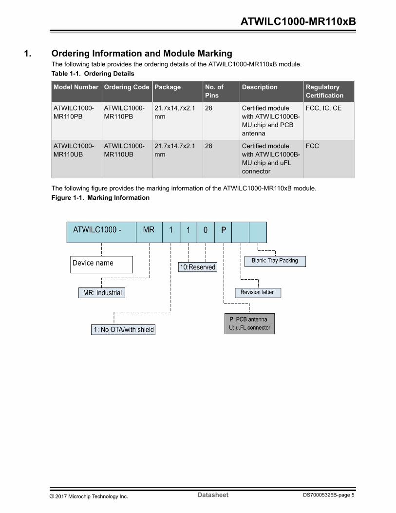
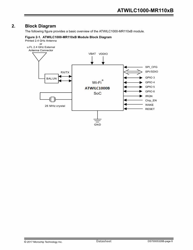
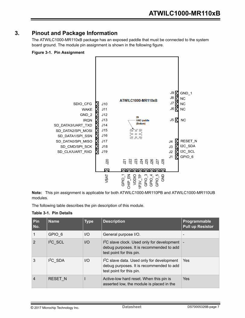
PinNo
Name Type Description ProgrammablePull up Resistor
SPI=I SDIO SPI Clock from ATWILC1000 whenmodule is configured for SPI
19 SD_CLK SDIO=I
UART=I
SDIO clock line for the ATWILC1000-MR110xB when module is configured forSDIO
Yes
20 VBATT Powersupply
Power supply pin for the DCDC convertor Yes
21 GPIO_1 IO General purpose IO Yes
22 CHIP_EN I Module enable High level enables modulelow level places module in power-downmode Connect to a host Output thatdefaults low at power-up If the host outputis tri-stated add a 1MΩ pull down resistor ifnecessary to ensure a low level at power-up
No
23 VDDIO Powersupply
IO power supply Must match host IOvoltage
-
24 1P3V_TP - 13V VDD Core Test Point Decouple with10uF and 001uF to GND
25 GPIO_3 IO General purpose IO By default UARTreceive input to ATWILC1000-MR110xBUsed only for development debugpurposes It is recommended to add testpoint for this pin
Yes
26 GPIO_4 IO General purpose IO Yes
27 GPIO_5 IO General purpose IO By default UARTtransmit output from ATWILC1000-MR110xB Used only for developmentdebug purposes It is recommended to addtest point for this pin
Yes
28 GND_3 Ground - -
29 Paddle Ground Exposed paddle GND This pad must besoldered to system ground
-
The following table provides the ATWILC1000-MR110xB module package dimensions
Table 3-2 ATWILC1000-MR110xB Module Package Information
Parameter Value Units
Package Size 2172 x 1473 mm
Pad Count 28 -
ATWILC1000-MR110xB
copy 2017 Microchip Technology Inc Datasheet DS70005326B-page 9
Parameter Value Units
Total Thickness 211 mm
Pad Pitch 1016
Pad Width 082
Exposed Pad size 37 x 37
ATWILC1000-MR110xB
copy 2017 Microchip Technology Inc Datasheet DS70005326B-page 10
4 Electrical Specifications
41 Absolute RatingsThe absolute maximum ratings for this module are listed in the following table
Table 4-1 ATWILC1000-MR110xB Module Absolute Maximum Ratings
Symbol Description Min Max Unit
VBATT Input supplyvoltage
-03 50 V
VDDIO IO voltage -03 50 V
Caution Stresses beyond those listed under Absolute Maximum Ratings cause permanentdamage to the device This is a stress rating only The functional operation of the device atthose or any other conditions above those indicated in the operation listings of this specificationis not implied Exposure to maximum rating conditions for extended periods affects the devicereliability
42 Recommended Operating ConditionsThe recommended operating conditions for this module is listed in the following table
Table 4-2 ATWILC1000-MR110xB Module Recommended Operating Conditions
Symbol Min Typ Max Unit
VBATT 30 33 42 V
VDDIO 18 33 36 V
Operatingtemperature
-40 +85 ordmC
Note 1 VBATT should be equal to or greater than VDDIO2 The voltage of VDDIO is dependent on system IO voltage3 Test Conditions -40ordmC to +85ordmC
43 Receiver PerformanceThe following are typical conditions for radio receiver performance
VBATT at 33 V VDDIO at 33V temperature at 25degC and WLAN Channel 6(2437 MHz)
The following table provides the receiver performance characteristics for this module
ATWILC1000-MR110xB
copy 2017 Microchip Technology Inc Datasheet DS70005326B-page 11
Table 4-3 Receiver Performance
Parameter Description Min Typ Max Unit
Frequency - 2412 - 2472 MHz
Sensitivity 80211b 1 Mbps DSSS - -94 -
dBm2 Mbps DSSS - -91 -
55 Mbps DSSS - -89 -
11 Mbps DSSS - -86 -
Sensitivity 80211g 6 Mbps OFDM - -88 -
dBm
9 Mbps OFDM - -87 -
12 Mbps OFDM - -86 -
18 Mbps OFDM - -84 -
24 Mbps OFDM - -82 -
36 Mbps OFDM - -78 -
48 Mbps OFDM - -74 -
54 Mbps OFDM - -73 -
Sensitivity 80211n (BW at 20 MHz) MCS 0 - -87 -
dBm
MCS 1 - -85 -
MCS 2 - -83 -
MCS 3 - -80 -
MCS 4 - -76 -
MCS 5 - -73 -
MCS 6 - -71 -
MCS 7 - -69 -
Maximum Receive Signal Level 1-11 Mbps DSSS 0 -
dBm6-54 Mbps OFDM -5 -
MCS 0 ndash 7 -5 -
Adjacent Channel Rejection 1 Mbps DSSS (30 MHz offset) - 50 -
dB
11 Mbps DSSS (25 MHz offset) - 43 -
6 Mbps OFDM (25 MHz offset) - 40 -
54 Mbps OFDM (25 MHz offset) - 25 -
MCS 0 ndash 20 MHz BW (25 MHz offset) - 40 -
MCS 7 ndash 20 MHz BW (25 MHz offset) - 20 -
Cellular Blocker Immunity 776-794 MHz CDMA - -14 -dBm
824-849 MHz GSM - -10 -
ATWILC1000-MR110xB
copy 2017 Microchip Technology Inc Datasheet DS70005326B-page 12
Parameter Description Min Typ Max Unit
880-915 MHz GSM - -10 -
1710-1785 MHz GSM - -15 -
1850-1910 MHz GSM - -15 -
1850-1910 MHz WCDMA - -24 -
1920-1980 MHz WCDMA - -24 -
44 Transmitter PerformanceThe following are typical conditions for radio transmitter performance
VBATT at 33 V VDDIO at 33V temperature at 25degC and WLAN Channel 6(2437 MHz)
The following table provides the transmitter performance characteristics for this module
Table 4-4 Transmitter Performance
Parameter Description Unit Minimum Typical Maximum
Frequency - MHz 2412 - 2472
Output Power1-2
ON_Transmit
80211b 1Mbps dBm - 176 -
80211b 11Mbps dBm - 182 -
80211g 6Mbps dBm - 187 -
80211g 54Mbps dBm - 167 -
80211n MCS 0 dBm - 173 -
80211n MCS 7 dBm - 138 -
Tx PowerAccuracy
- dB - plusmn152 -
CarrierSuppression
80211b mode dBc - -194 -
80211g mode dBc - -275 -
80211n mode dBc - -211 -
Out of BandTransmit Power
76-108 dBmHz - -125 -
776-794 dBmHz - -125 -
869-960 dBmHz - -125 -
925-960 dBmHz - -125 -
1570-1580 dBmHz - -125 -
1805-1880 dBmHz - -125 -
1930-1990 dBmHz - -125 -
2110-2170 dBmHz - -125 -
ATWILC1000-MR110xB
copy 2017 Microchip Technology Inc Datasheet DS70005326B-page 13
Parameter Description Unit Minimum Typical Maximum
HarmonicOutput Power4
2nd dBmMHz - -28 -
3rd dBmMHz - -33 -
4th dBmMHz - -40 -
5th dBmMHz - -28 -
Note 1 Measured at 80211 spec compliant EVMSpectral Mask2 Measured after RF matching network3 Operating temperature range is -40degC to +85degC RF performance is guaranteed at room
temperature of 25degC with a 2-3dB change at boundary conditions4 Measured at 11Mbps DG(Digital Gain)= -7 WLAN Channel 6 (2437 MHz)5 With respect to TX power different (higherlower) RF output power settings may be used for
specific antennas andor enclosures in which case recertification may be required6 The availability of some specific channels andor operational frequency bands are country
dependent and should be programmed at the Host product factory to match the intendeddestination Regulatory bodies prohibit exposing the settings to the end user This requirementneeds to be taken care of via Host implementation
45 Timing Characteristics
451 SPI TimingThe SPI slave interface supports four standard modes as determined by the Clock Polarity (CPOL) andClock Phase (CPHA) settings These modes are illustrated in the following table
Table 4-5 SPI Slave Modes
Mode CPOL CPHA
0 0 0
1 0 1
2 1 0
3 1 1
The red lines in the following figure correspond to clock phase at 0 and the blue lines correspond to clockphase at 1
ATWILC1000-MR110xB
copy 2017 Microchip Technology Inc Datasheet DS70005326B-page 14
Figure 4-1 SPI Slave Clock Polarity and Clock Phase Timing
z
z z
z
SCKCPOL = 0
CPOL = 1
SSN
RXDTXD(MOSIMISO)
CPHA = 0
CPHA = 1
2 3 4 5 6 7 8
1 2 3 4 5 6 7
1
8
The SPI timing is shown in the following figure
Figure 4-2 SPI Timing Diagram (SPI MODE CPOL=0 CPHA=0)
The SPI timing parameters are provided in the following table
Table 4-6 SPI Slave Timing Parameters1
Parameter Symbol Min Max Units
Clock Input Frequency2 fSCK - 48 MHz
Clock Low Pulse Width tWL 4 -ns
Clock High Pulse Width tWH 5 -
ATWILC1000-MR110xB
copy 2017 Microchip Technology Inc Datasheet DS70005326B-page 15
Parameter Symbol Min Max Units
Clock Rise Time tLH 0 7
Clock Fall Time tHL 0 7
TXD Output Delay3 tODLY 4 9 from SCK fall125 from SCKrise
RXD Input Setup Time tISU 1 -
RXD Input Hold Time tIHD 5 -
SSN Input Setup Time tSUSSN 3 -
SSN Input Hold Time tHDSSN 55 -
Note 1 Timing is applicable to all SPI modes2 Maximum clock frequency specified is limited by the SPI slave interface internal design actual
maximum clock frequency can be lower and depends on the specific PCB layout3 Timing is based on 15pF output loading
452 SDIO TimingThe SDIO Slave interface timing is shown in following figure
Figure 4-3 SDIO Timing Diagram
Slave timing parameters are provided in the following tableTable 4-7 SDIO Timing Parameters
Parameter Symbol Min Max Units
Clock InputFrequency1
fPP 0 50 MHz
Clock Low PulseWidth
tWL 9 - ns
ATWILC1000-MR110xB
copy 2017 Microchip Technology Inc Datasheet DS70005326B-page 16
Parameter Symbol Min Max Units
Clock High PulseWidth
tWH 45 -
Clock Rise Time tLH 0 5
Clock Fall Time tHL 0 5
Input Setup Time tISU 6 -
Input Hold Time tIH 4 -
Output Delay2 tODLY 3 11
1 Maximum clock frequency specified is limited by the SDIO Slave interface internal design actualmaximum clock frequency can be lower and depends on the specific PCB layout
2 Timing based on 15pF output loading
453 I2C TimingThe following figure illustrates I2C Slave timing
Figure 4-4 I2C Timing Diagram
The following table provides I2C Slave timing parameters
Table 4-8 I2C Timing Parameters
Parameter Symbol Min Max Units Remarks
SCL ClockFrequency
fSCL 0 400 kHZ -
SCL Low PulseWidth
tWL 13 - micros -
SCL High PulseWidth
tWH 06 - micros -
SCL SDA FallTime
tHL - 300 ns -
ATWILC1000-MR110xB
copy 2017 Microchip Technology Inc Datasheet DS70005326B-page 17
Parameter Symbol Min Max Units Remarks
SCL SDA RiseTime
tLH - 300 ns This is dictatedby externalcomponents
START SetupTime
tSUSTA 06 - micros -
START HoldTime
tHDSTA 06 - micros -
SDA SetupTime
tSUDAT 100 - ns -
SDA Hold Time tHDDAT 0 - ns Slave andMaster Default
MasterProgrammingOption
40 - ns
STOP Setuptime
tSUSTO 06 - micros -
Bus Free TimeBetween STOPand START
tBUF 13 - micros -
Glitch PulseReject
tPR 0 50 ns -
ATWILC1000-MR110xB
copy 2017 Microchip Technology Inc Datasheet DS70005326B-page 18
5 Power ManagementThe ATWILC1000-MR110xB module has several device states
bull On statesndash ON_Transmit ndash device actively transmits an 80211 signal Highest output power and nominal
current consumptionndash ON_Receive ndash device actively receivies an 80211 signal Lowest sensitivity and nominal
current consumptionndash ON_Doze ndash device is powered on but it does not actively transmit or receive the datandash Power_Down ndash device core supply is powered off
The following pins are used to switch between the ON and Power_Down statesbull CHIP_EN ndash this pin (pin 22) enables or disables the DCDC converterbull VDDIO ndash IO supply voltage from external supply
In the ON states VDDIO is ON and CHIP_EN is high (at VDDIO voltage level) To change from the ONstates to Power_Down state connect the RESETN and CHIP_EN pin to logic low (GND) by following thepower down sequence mentioned in Power-UpDown Sequence When VDDIO is off and CHIP_EN islow the chip is powered off with no leakage (also see Restrictions for Power States)
51 Current Consumption in Various Device StatesThe following table provides this modules current consumption in various device states
Table 5-1 Current Consumption
Device State Code Rate Output
Power (dBm)
Current Consumption1
IVBATT IVDDIO
ON_Transmit 80211b 1Mbps 176 266 mA 22 mA
80211b 11Mbps 185 239 mA 22 mA
80211g 6Mbps 186 249 mA 22 mA
80211g 54Mbps 169 173 mA 22 mA
80211n MCS 0 177 253 mA 22 mA
80211n MCS 7 140 164 mA 22 mA
ON_Receive 80211b 1Mbps NA 63 mA 22 mA
80211b 11Mbps NA 63 mA 22 mA
80211g 6Mbps NA 63 mA 22 mA
80211g 54Mbps NA 63 mA 22 mA
80211n MCS 0 NA 63 mA 22 mA
80211n MCS 7 NA 63 mA 22 mA
ATWILC1000-MR110xB
copy 2017 Microchip Technology Inc Datasheet DS70005326B-page 19
Device State Code Rate Output
Power (dBm)
Current Consumption1
ON_Doze NA NA 380microA lt10microA
Power_Down NA NA 125 uA(2)
Note 1 The power consumption values are measured when VBAT is 33V and VDDIO is 33V at 25degC2 Current consumption mentioned for these states is the sum of current consumed in VDDIO and
VBAT voltage rails
52 Restrictions for Power StatesWhen no power is supplied to the device the DCDC Converter output and VDDIO are both turned off (atground potential) In this case a voltage cannot be applied to the device pins because each pin containsan ESD diode from the pin to supply This diode will turn on when voltage higher than one diode-drop issupplied to the pin
If a voltage must be applied to the signal pads while the chip is in a low power state the VDDIO supplymust be on so the Sleep mode or power-down state must be used
Similarly to prevent the pin-to-ground diode from turning on do not apply a voltage that is more than onediode-drop below ground to any pin
53 Power-UpDown SequenceThe following figure illustrates the power-updown sequence for the ATWILC1000-MR110xB module
Figure 5-1 Power-UpDown Sequence
The following table provides power-updown sequence timing parameters
ATWILC1000-MR110xB
copy 2017 Microchip Technology Inc Datasheet DS70005326B-page 20
Table 5-2 Power-UpDown Sequence Timing
Parameter Min Max Units Description Notes
tA 0 - ms VBAT rise toVDDIO rise
VBAT and VDDIO can risesimultaneously or connected togetherVDDIO must not rise before VBAT
tB 0 - ms VDDIO rise toCHIP_EN rise
CHIP_EN must not rise before VDDIOCHIP_EN must be driven high or lowand must not be left floating
tC 5 - ms CHIP_EN rise toRESETN rise
This delay is required to stabilize the XOclock before RESETN removal RESETNmust be driven high or low and must notbe left floating
tArsquo 0 - ms VDDIO fall toVBAT fall
VBAT and VDDIO fall simultaneously orconnected together VBAT must not fallbefore VDDIO
tBrsquo 0 - ms CHIP_EN fall toVDDIO fall
VDDIO must not fall before CHIP_ENCHIP_EN and RESETN must fallsimultaneously
tCrsquo 0 - ms RESETN fall toVDDIO fall
VDDIO must not fall before RESETNRESETN and CHIP_EN fallsimultaneously
54 Digital IO Pin Behavior During Power-Up SequencesThe following table represents the digital IO pin states corresponding to the device power modes
Table 5-3 Digital IO Pin Behavior in Different Device States
Device State VDDIO CHIP_EN RESETN Output Driver InputDriver
Pull UpDownResistor (96
kOhm)
Power_Down coresupply OFF
High Low Low Disabled (Hi-Z) Disabled Disabled
Power-On Resetcore supply and hardreset ON
High High Low Disabled (Hi-Z) Disabled Enabled
Power-On Defaultcore supply ONdevice out of resetand not programmed
High High High Disabled (Hi-Z) Enabled Enabled
On_Doze
On_Transmit
High High High Programmedby firmware foreach pinenabled ordisabled
Oppositeof OutputDriverstate
Programmedby firmware foreach pinenabled ordisabled
ATWILC1000-MR110xB
copy 2017 Microchip Technology Inc Datasheet DS70005326B-page 21
Device State VDDIO CHIP_EN RESETN Output Driver InputDriver
Pull UpDownResistor (96
kOhm)
On_Receive coresupply ON deviceprogrammed byfirmware
ATWILC1000-MR110xB
copy 2017 Microchip Technology Inc Datasheet DS70005326B-page 22
6 CPU and Memory Subsystems
61 ProcessorThis ATWILC1000-MR110xB module has a Cortus APS3 32-bit processor This processor performs manyof the MAC functions including but not limited to association authentication power management securitykey management and MSDU aggregationdeaggregation In addition the processor provides flexibility forvarious modes of operation such as STA and AP modes
62 Memory SubsystemThe APS3 core uses a 128 KB instructionboot ROM along with a 160 KB instruction RAM and a 64 KBdata RAM In addition the device uses a 128 KB shared RAM accessible by the processor and MAC thatallows the APS3 core to perform various data management tasks on the Tx and Rx data packets
63 Nonvolatile Memory (eFuse)This ATWILC1000-MR110xB module has 768 bits of nonvolatile eFuse memory that is read by the CPUafter device reset This nonvolatile One-Time-Programmable (OTP) memory is used to store customerspecific parameters such as MAC address various calibration information such as Tx power crystalfrequency offset etc and other software-specific configuration parameters The eFuse is partitioned intosix 128 bit banks Each bank has the same bit map mentioned in the following figure The purpose of thefirst 80 bits in each bank is fixed and the remaining 48 bits are general purpose software dependent bitsEach bank is programmed independently which allows for several updates of the device parametersfollowing the initial programming For example if the MAC address has to be changed Bank 1 has to beprogrammed with the new MAC address along with the values of TX gain correction and Frequency offsetif they are used and programmed in the Bank 0 The contents of Bank 0 have to be invalidated in thiscase by programming the Invalid bit in the Bank 0 This will allow the firmware to use the MAC addressfrom Bank 1
By default all the ATWILC1000-MR110PB and ATWILC1000-MR110UB modules are programmed withthe MAC address and the Frequency offset bits of Bank 0
ATWILC1000-MR110xB
copy 2017 Microchip Technology Inc Datasheet DS70005326B-page 23
Figure 6-1 eFuse Bit Map
ATWILC1000-MR110xB
copy 2017 Microchip Technology Inc Datasheet DS70005326B-page 24
7 WLAN SubsystemThe WLAN subsystem is composed of the Media Access Controller (MAC) Physical Layer (PHY) andthe radio
71 MAC
711 DescriptionThis module is designed to operate at low power while providing high data throughput The IEEE 80211MAC functions are implemented with a combination of dedicated datapath engines hardwired controllogic and a low power high-efficiency microprocessor The combination of dedicated logic with aprogrammable processor provides optimal power efficiency and real time response while providing theflexibility to accommodate evolving standards and future feature enhancements
The dedicated datapath engines are used to implement data path functions with heavy computationalrequirements For example a Frame Check Sequence (FCS) engine checks the Cyclic RedundancyCheck (CRC) of the transmitting and receiving packets and a cipher engine performs all the requiredencryption and decryption operations for the WEP WPA-TKIP WPA2 CCMP-AES and WPA2 Enterprisesecurity requirements
Control functions which have real time requirements are implemented using hardwired control logicmodules These logic modules offer real time response while maintaining configurability through theprocessor Examples of hardwired control logic modules are the channel access control module(implements EDCAHCCA Beacon Tx control interframe spacing and so on) protocol timer module(responsible for the Network Access vector back-off timing timing synchronization function and slotmanagement) MAC Protocol Data Unit (MPDU) handling module aggregationdeaggregation moduleblock ACK controller (implements the protocol requirements for burst block communication) and TxRxcontrol Finite State Machine (FSM) (coordinate data movement between PHY and MAC interface cipherengine and the Direct Memory Acces (DMA) interface to the TxRx FIFOs)
Following are the characteristics of MAC functions implemented solely in software on the microprocessor
bull Functions with high memory requirements or complex data structures Examples are associationtable management and power save queuing
bull Functions with low computational load or without critical real time requirements Examples areauthentication and association
bull Functions that require flexibility and upgradeability Examples are beacon frame processing andQoS scheduling
712 FeaturesThe ATWILC1000-MR110xB IEEE 80211 MAC supports the following functions
bull IEEE 80211bgnbull IEEE 80211e WMM QoS EDCAPCF multiple access categories traffic schedulingbull Advanced IEEE 80211n features
ndash Transmission and reception of aggregated MPDUs (A-MPDU)ndash Transmission and reception of aggregated MSDUs (A-MSDU)ndash Immediate block acknowledgmentndash Reduced Interframe Spacing (RIFS)
bull Supports IEEE 80211i and WFA security with key management
ATWILC1000-MR110xB
copy 2017 Microchip Technology Inc Datasheet DS70005326B-page 25
ndash WEP 64128ndash WPA-TKIPndash 128-bit WPA2 CCMP (AES)ndash WPA2 Enterprise
bull Advanced power managementndash Standard IEEE 80211 Power save modendash Wi-Fi alliance WMM-PS (U-APSD)
bull RTS-CTS and CTS self supportbull Supports either STA or AP mode in the infrastructure basic service set modebull Supports concurrent mode of operationbull Supports Independent Basic Service Set (IBSS)
72 PHYThe ATWILC1000-MR110xB module WLAN PHY is designed to achieve reliable and power-efficientphysical layer communication specified by IEEE 80211 bgn in single stream mode with 20 MHzbandwidth The advanced algorithms are used to achieve maximum throughput in a real worldcommunication environment with impairments and interference The PHY implements all the requiredfunctions such as Fast Fourier Transform (FFT) filtering Forward Error Correction (FEC) that is a Viterbidecoder frequency timing acquisition and tracking channel estimation and equalization carrier sensingclear channel assessment and automatic gain control
Features
The IEEE 80211 PHY supports the following functions
bull Single antenna 1x1 stream in 20 MHz channelsbull Supports IEEE 80211b DSSS-CCK modulation 1 2 55 and 11 Mbpsbull Supports IEEE 80211g OFDM modulation 6 9 1218 24 36 48 and 54 Mbpsbull Supports IEEE 80211n HT modulations MCS0-7 20 MHz 800 and 400ns guard interval 65 72
130 144 195 217 260 289 390 433 520 578 585 650 and 722 Mbpsbull IEEE 80211n mixed mode operationbull Per packet Tx power controlbull Advanced channel estimationequalization automatic gain control CCA carriersymbol recovery
and frame detection
721 FeaturesThe IEEE 80211 PHY supports the following functions
bull Single antenna 1x1 stream in 20 MHz channelsbull Supports IEEE 80211b DSSS-CCK modulation 1 2 55 and 11 Mbpsbull Supports IEEE 80211g OFDM modulation 6 9 1218 24 36 48 and 54 Mbpsbull Supports IEEE 80211n HT modulations MCS0-7 20 MHz 800 and 400ns guard interval 65 72
130 144 195 217 260 289 390 433 520 578 585 650 and 722 Mbpsbull IEEE 80211n mixed mode operationbull Per packet Tx power controlbull Advanced channel estimationequalization automatic gain control CCA carriersymbol recovery
and frame detection
ATWILC1000-MR110xB
copy 2017 Microchip Technology Inc Datasheet DS70005326B-page 26
73 RadioThis section describes the properties and characteristics of the ATWILC1000- MR110xB and Wi-Fi radiotransmit and receive performance capabilities of the device The performance measurements are taken atthe RF pin assuming 50Ω impedance the RF performance is guaranteed for room temperature of 25degCwith a derating of 2-3dB at boundary conditions
Measurements were taken under typical conditions VBATT at 33V VDDIO at 33V and temperature at+25ordmC
Table 7-1 Features and Properties
Feature Description
Module Part Number ATWILC1000-MR110xB
WLAN Standard IEEE 80211bgn Wi-Fi compliant
Host Interface SPI SDIO
Dimension L x W x H 217 x 147 x 21 (typical) mm
Frequency range 2412 GHz ~ 2472 GHz (24 GHz ISM band)
Number of channels 11 for North America 13 for Europe
Modulation 80211b DQPSK DBPSK CCK
80211gn OFDM64-QAM16-QAM QPSK BPSK
Data rate 80211b 1 2 55 11 Mbps80211g 6 9 12 18 24 36 48 54 Mbps
Data rate
(20 MHz short GI400ns)
80211n 72 144 217 289 433 578 65722Mbps
Operating temperature(1) -40degC to 85degC
Storage temperature -40degC to 125degC
Humidity Operating humidity 10 to 95 non-condensing
Storage humidity 5 to 95 non-condensing
Note 1 RF performance is guaranteed at room temperature of 25degC with a 2-3db change at boundary
conditions
ATWILC1000-MR110xB
copy 2017 Microchip Technology Inc Datasheet DS70005326B-page 27
8 External InterfacesThis section describes the various host and debug interfaces of the ATWILC1000-MR110xB module
81 Interfacing with the Host MicrocontrollerThis section describes how to interface ATWILC1000-MR110xB module with the host microcontroller Theinterface comprises of a slave SPISDIO and additional control signals as shown in the figure Additionalcontrol signals are connected to the GPIOIRQ interface of the microcontroller
Figure 8-1 Interfacing with the Host Microcontroller
Table 8-1 Host Microcontroller Interface Pins
Module Pin Function(1)
4 RESET_N
11 WAKE
13 IRQ_N
22 CHIP_EN
16 SPI_SSNSD_DATA1
15 SPI_MOSISD_DATA2
17 SPI_MISOSD_DATA0
18 SPI_SCKSD_CMD
ATWILC1000-MR110xB
copy 2017 Microchip Technology Inc Datasheet DS70005326B-page 28
Module Pin Function(1)
14 SD_DATA3
19 SD_CLK
Note 1 Logic input for module pin SDIO_SPI_CFG(10) determines whether SDIO or SPI slave interface is
enabled Connect SDIO_SPI_CFG to VDDIO through a 1MΩ resistor to enable the SPI interfaceConnect SDIO_SPI_CFG to ground to enable SDIO interface
2 It is recommended to place test points for pins I2C_SDA(3) I2C_SCL(2) GPIO_3(25) andGPIO_5(27) in the design
82 SPI Slave InterfaceThe SPI slave interface can be enabled by connecting the SDIO_SPI_CFG pin to VDDIO This SPIinterface is used to exchange the control and 80211 data The SPI is a full duplex slave-synchronousserial interface that is available following reset when pin 10 (SDIO_SPI_CFG) is connected to VDDIO
The SPI interface pin mapping configuration is provided in the following table
Table 8-2 SPI Interface Pin Mapping
Pin SPI Function
10 SDIO_SPI_CFG Must be connected to VDDIO
16 SSN Active-Low Slave Select
15 MOSI Serial Data Receive
18 SCK Serial Clock
17 MISO Serial Data Transmit
When the SPI is not selected ie when SSN is high the SPI interface will not interfere with datatransfers between the serial master and other serial slave devices When the serial slave is not selectedits transmitted data output is buffered resulting in a high impedance drive onto the MISO line
The SPI interface responds to a protocol that allows an external host to read or write any register in thechip and also initiate DMA transfers
The SPI SSN MOSI MISO and SCK pins of this module have internal programmable pull up resistorsThese resistors are programmed to be disabled Otherwise if any of the SPI pins are driven to a low levelwhile this module is in the low power sleep state current will flow from the VDDIO supply through the pullup resistors increasing the current consumption of the module
83 SDIO Slave InterfaceThe SDIO interface is enabled by connecting the SDIO_SPI_CFG pin to ground This SDIO interface isused to exchange the control and 80211 data The SDIO interface is available after reset when pin 10(SDIO_SPI_CFG) is connected to ground
This SDIO is a full speed interface The interface supports the 1-bit4-bit SD transfer mode at the clockrange of 0-50 MHz The host uses this interface to read and write from any register within the chip andalso configures this module for DMA data transfer
ATWILC1000-MR110xB
copy 2017 Microchip Technology Inc Datasheet DS70005326B-page 29
The SDIO interface pin mapping configuration is provided in the following table
Table 8-3 ATWILC1000 SDIO Interface Pin Mapping
Pin SDIO Function
10 SDIO_SPI_CFG Must be connected to ground
14 DAT3 Data 3
15 DAT2 Data 2
16 DAT1 Data 1
17 DAT0 Data 0
18 CMD Command
19 CLK Clock
The SDIO card is detected when the it is inserted into an SDIO host During the normal initialization andinterrogation of the card by the host the card identifies itself as an SDIO device The host softwareobtains the card information in a tuple (linked list) format and determines if that cardrsquos IO function(s) areacceptable to activate If the card is acceptable it is allowed to power-up fully and start the IO function(s)built into the card
The SD memory card communication is based on an advanced 9-pin interface (clock command fourdata and three power lines) designed to operate at maximum operating frequency of 50 MHz
831 Featuresbull Compliant with SDIO card specification version 20bull Host clock rate variable between 0 and 50 MHzbull Supports 1-bit4-bit SD bus modesbull Allows card to interrupt hostbull Responds to direct readwrite (IO52) and extended readwrite (IO53) transactionsbull Supports suspendresume operation
84 UART Debug InterfaceThis module has a Universal Asynchronous ReceiverTransmitter (UART) interface on J25(RxD) andJ27(TxD) pins This interface should be used only for debugging purposes The UART is compatible withthe RS-232 standard where ATWILC1000-MR110xB operates as Data Terminal Equipment (DTE) It hasa two-pin RXDTXD interface
The default configuration for accessing the UART interface of ATWILC1000-MR110xB is mentionedbelow
bull Baud rate 115200bull Data 8 bitbull Parity Nonebull Stop bit 1 bitbull Flow control None
It also has Rx and Tx FIFOs which ensures reliable high speed reception and low software overheadtransmission FIFO size is 4x8 for both Rx and Tx direction The UART has status registers that show the
ATWILC1000-MR110xB
copy 2017 Microchip Technology Inc Datasheet DS70005326B-page 30
number of received characters available in the FIFO and various error conditions in addition it has theability to generate interrupts based on these status bits
An example of UART receiving or transmitting a single packet is shown in the following figure Thisexample shows 7-bit data (0x45) odd parity and two stop bits
Figure 8-2 Example of UART RX or TX Packet
85 I2C Slave InterfaceThis module provides an I2C bus slave that allows for easy debugging of the ATWILC1000-MR110xBdevices It supports I2C bus Version 21 ndash 2000
The I2C interface is used only for debug This interface is a two-wire serial interface consisting of a serialdata line (SDA Pin 17) and a serial clock (SCL Pin 18) It responds to seven bit address value 0x60This module I2C interface operates in standard mode (with data rates up to 100Kbs) and fast mode (withdata rates up to 400Kbs)
The I2C is a synchronous serial interface The SDA line is a bidirectional signal and changes only whenthe SCL line is low except for STOP START and RESTART conditions The output drivers are open-drain to perform wire AND functions on the bus The devices on the bus are limited to the 400pFcapacitance Data is transmitted in byte packages
For specific information refer to the Philips Specification entitled ldquoThe I2C -Bus Specification Version21rdquo
ATWILC1000-MR110xB
copy 2017 Microchip Technology Inc Datasheet DS70005326B-page 31
9 Notes on Interfacing with the ATWILC1000-MR110xBProgrammable Pull up Resistors
The ATWILC1000-MR110xB module provides programmable pull up resistors on various pins Thepurpose of these resistors is to keep any unused input pins from floating which causes excess current toflow through the input buffer from the VDDIO supply Any unused pin on the device must leave these pullup resistors enabled so that the pin will not float The default state at power-up is for the pull up resistorto be enabled however any pin that is used must have the pull up resistor disabled The reason for thisis that if any pins are driven to a low level while the device is in the low power sleep state current flowsfrom the VDDIO supply through the pull up resistors increasing the current consumption of the moduleSince the value of the pull up resistor is approximately 100 kOhm the current through any pull up resistorthat is being driven low is VDDIO100K For VDDIO = 33V the current is approximately 33 microA The pinsthat are used and have programmable the pull up resistor disabled should always be actively driven toeither a high or low level and not be allowed to float
ATWILC1000-MR110xB
copy 2017 Microchip Technology Inc Datasheet DS70005326B-page 32
10 Application Reference DesignThis section provides reference schematic for ATWILC1000-MR110xB module with SPI and SDIO hostinterfacesFigure 10-1 ATWILC1000-MR110xB Reference Schetmatic - SDIO Host Interface
Table 10-1 ATWILC1000-MR110xB reference Schematic - SDIO Host Interface - Bill of Materials
Item Qty Reference Value Description
Manufacturer
PartNumber
Footprint
1 9 R2 R3R4R5 R6R7 R8R9 R10
0 R RESISTORThick Film0 ohm0402
Yageo RC0402JR-070RL
0402
2 1 U1 ATWILC1000-MR110xB
Wi-FiModule
Microchip ATWILC1000-MR110xB
ATWILC1000-MR110xB
copy 2017 Microchip Technology Inc Datasheet DS70005326B-page 33
Figure 10-2 ATWILC1000-MR110xB Reference Schetmatic - SPI Host Interface
Table 10-2 ATWILC1000-MR110xB reference Schematic - SPI Host Interface - Bill of Materials
Item Qty Reference Value Description
Manufacturer
PartNumber
Footprint
1 1 R1 1 M RESISTORThick Film1 M ohm0402
Yageo RC0100FR-071ML
0402
2 9 R2 R3R4R5 R6R7 R8R9 R10
0 R RESISTORThick Film0 ohm0402
Yageo RC0402JR-070RL
0402
3 1 U1 ATWILC1000-MR110xB
Wi-FiModule
Microchip ATWILC1000-MR110xB
ATWILC1000-MR110xB
copy 2017 Microchip Technology Inc Datasheet DS70005326B-page 34
11 Module Outline DrawingsThe ATWILC1000-MR110PB module package details are outlined in the following figure Dimensions arein mm
Figure 11-1 Module Drawings ndash ATWILC1000-MR110PB - Top Bottom and Side Views
MODULE TOP VIEW
Metal Shield
Metal Shield
PCB
MODULE SIDE VIEW MODULE BOTTOM VIEW
NOTE THIS PAD MUST BE SOLDERED TO GND
NOT TO SCALE
The ATWILC1000-MR110UB module package details are outlined in the following figure Dimensions arein mm
ATWILC1000-MR110xB
copy 2017 Microchip Technology Inc Datasheet DS70005326B-page 35
Figure 11-2 Module Drawings ndash ATWILC1000-MR110UB - Top Bottom and Side Views
MODULE TOP VIEW
Metal Shield
Metal Shield
PCB
MODULE SIDE VIEW MODULE BOTTOM VIEW
NOTE THIS PAD MUST BE SOLDERED TO GND
NOT TO SCALE Rev 2
This section provides the outline drawing for the recommended footprint for the ATWILC1000-MR110xBmodule It is imperative that the center Ground Pad is provided with an array of GND vias to provide agood ground and act as thermal sink for the ATWILC1000-MR110xB module
ATWILC1000-MR110xB
copy 2017 Microchip Technology Inc Datasheet DS70005326B-page 36
Figure 11-3 Recommended Solder Pad Footprint
NOTE THIS PAD MUST BE TIED TO GND
1016 Pitch
1473
19
08
1016 Pitch
4064
267
267
600
1016 Pitch
370
370
1016 Pitch
19 3048
368
2172 2032
442
SOLDER PAD FOOTPRINT
Drawing not to scaleUntoleranced dimensionsUnits=mm
ATWILC1000-MR110xB
copy 2017 Microchip Technology Inc Datasheet DS70005326B-page 37
12 Design ConsiderationThis section provides the guidelines on placement and routing to achieve the best performance
121 ATWILC1000-MR110PB Placement and Routing GuidelinesIt is critical to follow the recommendations listed below to achieve the best RF performance
bull The module must be placed on host board The printed antenna area must overlap with the carrierboard The portion of the module containing the antenna should not stick out over the edge of thehost board The antenna is designed to work properly when it is sitting directly on top of a 15mmthick printed circuit board Figure 12-2 shows the best poor and worst case module placements inhost board
bull If the module is placed at the edge of the host board a minimum 22mm by 5 mm area directlyunder the antenna must be clear of all metal on all layers of the board ldquoIn-landrdquo placement isacceptable however deepness of keep-out area must grove to module edge to host board edgeplus 5 mmNote Do not place the module in the middle of the host board or far away from the host boardedge
bull Follow the module placement keepout host PCB cutout recommendation as shown in Figure 12-1ndash Avoid routing any traces in the highlighted region on the top layer of the host board which will
be directly below the module areandash Follow the electrical keepout layer recommendation as shown in Figure 12-1 There should be
no copper in all layers of the host board in this region Avoid placing any components (likemechanical spacers bumpon etc) in the recommended electrical keepout area
ndash Place GND polygon pour below the module with the recommended boundary in the top layerof the host board as shown in Figure 12-1 Do not have any breaks in this GND plane
ndash Place sufficient GND vias in the highlighted area below the module for better RFperformance
ndash It is recommended to have a 3x3 grid of GND vias solidly connecting the exposed GNDpaddle of the module to the inner layer ground plane This will act as a good ground andthermal conduction for the ATWILC1000-MR110PB module The GND vias should have aminimum via hole size of 03mm
ndash Follow the mechanical boundary of the host PCB as shown in the Figure 12-1bull Keep the large metal objects away from antenna to avoid electromagnetic field blockingbull Do not enclose the antenna within a metal shieldbull Keep any components which may radiate noise or signals within the 24 GHz ndash 25 GHz frequency
band away from the antenna and if possible shield those components Any noise radiated from thehost board in this frequency band will degrade the sensitivity of the module
bull Make sure the width of the traces routed to GND VDDIO and VBAT rails are sufficiently larger forhandling the peak Tx current consumption
ATWILC1000-MR110xB
copy 2017 Microchip Technology Inc Datasheet DS70005326B-page 38
Figure 12-1 ATWILC1000-MR110PB Placement Reference
Figure 12-2 ATWILC1000-MR110PB Placement Example
122 Printed PCB Antenna Performance of ATWILC1000-MR110PBThe printed PCB antenna on the ATWILC1000-MR110PB is a meandered Inverted F Antenna (IFA) Theantenna is fed via matching network which is matched for the module installed on 15mm thick mainboard Main board thickness deviation by plusmn1mm changes RXTX performance by plusmn1dB maximumreferring to RXTX performance with default antenna matching network and installed on 15mm thick mainboard
Measured antenna gain is -03dBi
ATWILC1000-MR110xB
copy 2017 Microchip Technology Inc Datasheet DS70005326B-page 39
Antenna Radiation PatternFollowing figures illustrate the antenna radiation pattern During the measurement the printed antenna isplaced in the XZ plane with Y axis being perpendicular to the module and pointing to the back of themoduleFigure 12-3 Antenna Radiation Pattern when Phi = 0 degree
Figure 12-4 Antenna Radiation Pattern when Phi = 90 degree
ATWILC1000-MR110xB
copy 2017 Microchip Technology Inc Datasheet DS70005326B-page 40
Figure 12-5 Antenna Radiation Pattern when Theta = 90 degree
ATWILC1000-MR110xB
copy 2017 Microchip Technology Inc Datasheet DS70005326B-page 41
123 ATWILC1000-MR110UB Placement and Routing GuidelinesThe ATWILC1000-MR110UB module has an Ultra Small Miniature RF Connector (uFL) for the externalantenna
The choice of antenna is limited to the antenna types for which the module was tested and approved Fora list of tested and approved antennas that may be used with the module refer to the respective countryin the Regulatory Approval section
An approved and tested antenna type is shown in the following Table
Table 12-1 Tested External Antenna Type
Antenna Type Gain
PCB Antenna 20 dBi
ATWILC1000-MR110xB
copy 2017 Microchip Technology Inc Datasheet DS70005326B-page 42
1231 Recommended External Antenna for ATWILC1000-MR110UBPCB Antenna (Part number W3525B039) along with a 10cm length RF cable assembly (uFL to SMA)has been used for the certification of ATWILC1000-MR110UB It is recommended to use the same orsimilar external antenna in design
ATWILC1000-MR110xB
copy 2017 Microchip Technology Inc Datasheet DS70005326B-page 43
13 Reflow Profile InformationThis section provides the guidelines for the reflow process to get the module soldered to the customersdesign
131 Storage Condition
1311 Moisture Barrier Bag Before OpeningA moisture barrier bag must be stored in a temperature of less than 30degC with humidity under 85 RHThe calculated shelf life for the dry-packed product shall be 12 months from the date the bag is sealed
1312 Moisture Barrier Bag OpenHumidity indicator cards must be blue indicating that the humidity is lt30
132 Solder PasteSnAgCu eutectic solder with melting temperature of 217degC is most commonly used for lead-free solderreflow application This alloy is widely accepted in the semiconductor industry due to its low costrelatively low melting temperature and good thermal fatigue resistance Some recommended pastesinclude NC-SMQreg 230 flux and Indalloyreg 241 solder paste made up of 955 Sn38 Ag07 Cu or SENJUN705-GRN3360-K2-V Type 3 no clean paste
133 Stencil DesignThe recommended stencil is laser-cut stainless-steel type with thickness of 100 microm to 130 microm andapproximately a 11 ratio of stencil opening to pad dimension To improve paste release a positive taperwith bottom opening 25 microm larger than the top is utilized Local manufacturing experience may find othercombinations of stencil thickness and aperture size to get good results
134 Printing ProcessThe printing process requires no significant changes compared to SnPb solder Any guidelinesrecommended by the paste manufacturers to accommodate paste specific characteristics should befollowed Post-print inspection and paste volume measurement is very critical to ensure good print qualityand uniform paste
135 Baking ConditionsThis module is rated at MSL level 3 After the sealed bag is opened no baking is required within 168hours as long as the devices are held at le 30degC60 RH or stored at lt 10 RH
The module requires baking before mounting ifbull The sealed bag has been open for more than 168 hoursbull The humidity indicator card reads more than 10bull SIPs need to be baked for eight hours at 125degC
ATWILC1000-MR110xB
copy 2017 Microchip Technology Inc Datasheet DS70005326B-page 44
136 Soldering and Reflow ConditionOptimization of the reflow process is the most critical factor considered for lead-free soldering Thedevelopment of an optimal profile must account the paste characteristics the size of the board thedensity of the components the mix of the larger and smaller components and the peak temperaturerequirements of the components An optimized reflow process is the key to ensuring a successful lead-free assembly and achieves high yield and long-term solder joint reliability
Temperature ProfilingTemperature profiling must be performed for all new board designs by attaching thermocouples at thesolder joints on the top surface of the larger components and at multiple locations of the boards This isto ensure that all components are heated to a temperature above the minimum reflow temperatures andthe smaller components do not exceed the maximum temperature limit The SnAgCu solder alloy melts at~217degC so the reflow temperature peak at joint level must be 15 to 20degC higher than meltingtemperature The targeted solder joint temperature for the SnAgCu solder must be ~235degC For larger orsophisticated boards with a large mix of components it is also important to ensure that the temperaturedifference across the board is less than 10 degrees to minimize board warpage The maximumtemperature at the component body must not exceed the MSL3 qualification specification
1361 Reflow OvenIt is strongly recommended that a reflow oven equipped with more heating zones and Nitrogenatmosphere be used for lead-free assembly Nitrogen atmosphere has shown to improve the wet-abilityand reduce temperature gradient across the board It can also enhance the appearance of the solderjoints by reducing the effects of oxidation
The following items should also be observed in the reflow process1 Some recommended pastes include
ndash NC-SMQreg 230 flux and Indalloyreg 241 solder paste made up of 955 Sn38 Ag07 Cundash SENJU N705-GRN3360-K2-V Type 3 no clean paste
2 Allowable reflow soldering iterationsndash Three times based on the following reflow soldering profile (refer following Figure)
3 Temperature profilendash Reflow soldering shall be done according to the following temperature profile (refer to the
following figure)ndash Peak temperature 250degC
ATWILC1000-MR110xB
copy 2017 Microchip Technology Inc Datasheet DS70005326B-page 45
Figure 13-1 Solder Reflow Profile
Cleaning
The exposed ground paddle helps to self-align the module avoiding pad misalignment The use of no-clean solder pastes is recommended Full drying of no-clean paste fluxes must be ensured as a result ofthe reflow process This may require longer reflow profiles andor peak temperatures toward the high endof the process window as recommended by the solder paste vendor It is believed that uncured fluxresidues could lead to corrosion andor shorting in accelerated testing and possibly the field
Rework
Rework is to remove the mounted SIP package and replace with a new unit It is recommended that oncean ATWILC1000-MR110xB module has been removed it should never be reused During the reworkprocess the mounted module and PCB are heated partially and the module is removed It isrecommended to heat-proof the proximity of the mounted parts and junctions and use the best nozzle forrework that is suited to the module size
ATWILC1000-MR110xB
copy 2017 Microchip Technology Inc Datasheet DS70005326B-page 46
14 Module Assembly ConsiderationsThe ATWILC1000-MR110xB modules are assembled with an EMI Shield to ensure compliance with EMIemission and immunity rules The EMI shield is made of a tin-plated steel (SPTE) and is not hermeticallysealed Solutions like IPA and similar solvents can be used to clean the ATWILC1000-MR110xB modulehowever cleaning solutions that contain acid should never be used on the module
The ATWILC1000-MR110xB modules are manufactured without any conformal coating applied It is thecustomerrsquos responsibility if a conformal coating is specified and applied to the ATWILC1000- MR110xBmodule
ATWILC1000-MR110xB
copy 2017 Microchip Technology Inc Datasheet DS70005326B-page 47
15 Regulatory ApprovalRegulatory approvals received
ATWILC1000-MR110PBbull United StatesFCC ID 2ADHKATWILC1000bull CanadaISED
ndash IC 20266-ATWILC1000ndash HVIN ATWILC1000-MR110PB
bull Europe - CE
ATWILC1000-MR110UBbull United StatesFCC ID 2ADHKATWILC1000U
151 United StatesThe ATWILC1000-MR110PB and ATWILC1000-MR110UB modules have received FederalCommunications Commission (FCC) CFR47 Telecommunications Part 15 Subpart C ldquoIntentionalRadiatorsrdquo single-modular approval in accordance with Part 15212 Modular Transmitter approval Single-modular transmitter approval is defined as a complete RF transmission sub-assembly designed to beincorporated into another device that must demonstrate compliance with FCC rules and policiesindependent of any host A transmitter with a modular grant can be installed in different end-use products(referred to as a host host product or host device) by the grantee or other equipment manufacturer thenthe host product may not require additional testing or equipment authorization for the transmitter functionprovided by that specific module or limited module device
The user must comply with all of the instructions provided by the Grantee which indicate installationandor operating conditions necessary for compliance
A host product itself is required to comply with all other applicable FCC equipment authorizationregulations requirements and equipment functions that are not associated with the transmitter moduleportion For example compliance must be demonstrated to regulations for other transmitter componentswithin a host product to requirements for unintentional radiators (Part 15 Subpart B) such as digitaldevices computer peripherals radio receivers etc and to additional authorization requirements for thenon-transmitter functions on the transmitter module (ie Verification or Declaration of Conformity) asappropriate (eg Bluetooth and Wi-Fi transmitter modules may also contain digital logic functions)
1511 Labeling and User Information RequirementsThe ATWILC1000-MR110PB and ATWILC1000-MR110UB modules have been labeled with their ownFCC ID numbers If the FCC ID is not visible when the module is installed inside another device then theoutside of the finished product into which the module is installed must display a label referring to theenclosed module This exterior label can use wording as follows
For the ATWILC1000-MR110PB
Contains Transmitter Module FCC ID 2ADHKATWILC1000 or
Contains FCC ID 2ADHKATWILC1000
This device complies with Part 15 of the FCC Rules Operation is subject to the following twoconditions (1) this device may not cause harmful interference and (2) this device must acceptany interference received including interference that may cause undesired operation
ATWILC1000-MR110xB
copy 2017 Microchip Technology Inc Datasheet DS70005326B-page 48
For the ATWILC1000-MR110UB
Contains Transmitter Module FCC ID 2ADHKATWILC1000U or
Contains FCC ID 2ADHKATWILC1000U
This device complies with Part 15 of the FCC Rules Operation is subject to the following twoconditions (1) this device may not cause harmful interference and (2) this device must acceptany interference received including interference that may cause undesired operation
A users manual for the finished product should include the following statement
This equipment has been tested and found to comply with the limits for a Class B digital devicepursuant to part 15 of the FCC Rules These limits are designed to provide reasonable protectionagainst harmful interference in a residential installation This equipment generates uses and can radiateradio frequency energy and if not installed and used in accordance with the instructions may causeharmful interference to radio communications However there is no guarantee interference will not occurin a particular installation If this equipment does cause harmful interference to radio or televisionreception which can be determined by turning the equipment off and on the user is encouraged to tryto correct the interference by one or more of the following measures
bull Reorient or relocate the receiving antennabull Increase the separation between the equipment and receiverbull Connect the equipment into an outlet on a circuit different from that to which the receiver is
connectedbull Consult the dealer or an experienced radioTV technician for help
Additional information on labeling and user information requirements for Part 15 devices can be found inKDB Publication 784748 which is available at the FCC Office of Engineering and Technology (OET)Laboratory Division Knowledge Database (KDB) httpsappsfccgovoetcfkdbindexcfm
1512 RF ExposureAll transmitters regulated by FCC must comply with RF exposure requirements KDB 447498 General RFExposure Guidance provides guidance in determining whether proposed or existing transmitting facilitiesoperations or devices comply with limits for human exposure to Radio Frequency (RF) fields adopted bythe Federal Communications Commission (FCC)
From the FCC Grant Output power listed is conducted This transmitter is restricted for use with thespecific antenna(s) tested in this application for Certification
In the end product the antenna(s) used with this transmitter must be installed to provide a separationdistance of at least 65 cm from all persons and must not be co-located or operation in conjunction withany other antenna or transmitter User and installers must be provided with antenna installationinstructions and transmitter operating conditions for satisfying the RF exposure compliance
1513 Approved Antenna TypesTo maintain modular approval in the United States only the antenna types that have been tested shall beused It is permissible to use a different antenna provided the same antenna type and antenna gain(equal to or less than) is used An antenna type comprises antennas having similar in-band and out-of-band radiation patterns
Testing the ATWILC1000-MR110UB module was performed with the antenna types listed in Table 12-1
ATWILC1000-MR110xB
copy 2017 Microchip Technology Inc Datasheet DS70005326B-page 49
1514 Helpful WebsitesFederal Communications Commission (FCC) httpwwwfccgov
FCC Office of Engineering and Technology (OET) Laboratory Division Knowledge Database (KDB) httpsappsfccgovoetcfkdbindexcfm
152 CanadaThe ATWILC1000-MR110PB module has been certified for use in Canada under Innova- tion Scienceand Economic Development Canada (ISED formerly Industry Canada) Radio Standards Procedure(RSP) RSP-100 Radio Standards Specifi- cation (RSS) RSS-Gen and RSS-247 Modular approvalpermits the installation of a module in a host device without the need to recertify the device
1521 Labeling and User Information RequirementsLabel Requirements (from RSP-100 Issue 11 Section 3) The host device shall be properly labeled toidentify the module within the host device
The Innovation Science and Economic Development Canada certification label of a module shall beclearly visible at all times when installed in the host device otherwise the host device must be labeled todisplay the Innovation Science and Economic Development Canada certification number of the modulepreceded by the words ldquoContainsrdquo or similar wording expressing the same meaning as follows
For the ATWILC1000-MR110PB
Contains IC 20266-ATWILC1000
User Manual Notice for License-Exempt Radio Apparatus (from Section 84 RSS-Gen Issue 4November 2014) User manuals for license-exempt radio apparatus shall contain the following orequivalent notice in a conspicuous location in the user manual or alternatively on the device or both
This device complies with Industry Canada license exempt RSS standard(s) Operation issubject to the following two conditions
(1) This device may not cause interference and
(2) This device must accept any interference including interference that may cause undesiredoperation of the device
Le preacutesent appareil est conforme aux CNR dIndustrie Canada applicables aux appareils radioexempts de licence Lexploitation est autoriseacutee aux deux conditions suivantes
(1) lappareil ne doit pas produire de brouillage et
(2) lutilisateur de lappareil doit accepter tout brouillage radioeacutelectrique subi mecircme si lebrouillage est susceptible den compromettre le fonctionnement
Guidelines on Transmitter Antenna for License Exempt Radio Apparatus
Under Industry Canada regulations this radio transmitter may only operate using an antenna ofa type and maximum (or lesser) gain approved for the transmitter by Industry Canada To reducepotential radio interference to other users the antenna type and its gain should be so chosenthat the equivalent isotropically radiated power (eirp) is not more than that necessary forsuccessful communication
Conformeacutement agrave la reacuteglementation dIndustrie Canada le preacutesent eacutemetteur radio peutfonctionner avec une antenne dun type et dun gain maximal (ou infeacuterieur) approuveacute pour
ATWILC1000-MR110xB
copy 2017 Microchip Technology Inc Datasheet DS70005326B-page 50
leacutemetteur par Industrie Canada Dans le but de reacuteduire les risques de brouillage radioeacutelectriqueagrave lintention des autres utilisateurs il faut choisir le type dantenne et son gain de sorte que lapuissance isotrope rayonneacutee eacutequivalente (pire) ne deacutepasse pas lintensiteacute neacutecessaire agraveleacutetablisse-ment dune communication satisfaisante
1522 RF ExposureAll transmitters regulated by Innovation Science and Economic Development Canada (ISED) mustcomply with RF exposure requirements listed in RSS-102 - Radio Frequency (RF) Exposure Complianceof Radio communication Apparatus (All Frequency Bands)
This transmitter is restricted for use with a specific antenna tested in this application for certification andmust not be co-located or operating in conjunction with any other antenna or transmitters within a hostdevice except in accordance with Canada multi-transmitter product procedures
The installation of the transmitter must ensure that the antenna has a separation distance of at least 65cm from all persons or compliance must be demonstrated according to the ISED SAR procedures
1523 Canada_Helpful WebsitesInnovation Science and Economic Development Canada httpwwwicgcca
153 EuropeThe ATWILC1000-MR110PB module is Radio Equipment Directive (RED) assessed radio module that isCE marked and have been manufactured and tested with the intention of being integrated into a finalproduct
The ATWILC1000-MR110PB module has been tested to RED 201453EU Essential Requirements forHealth and Safety (Article (31(a)) Electromagnetic Compatibility (EMC) (Article 31(b)) and Radio(Article 32) and are summarized in Table 15-1
The ETSI provides guidance on modular devices in ldquoGuide to the application of harmonised standardscovering articles 31b and 32 of the RED 201453EU (RED) to multi-radio and combined radio and non-radio equipmentrdquo document available at httpwwwetsiorgdeliveretsi_eg203300_203399203367010101_60eg_203367v010101ppdf
Note To maintain conformance to the testing listed in Table 15-1 the module shall be installed inaccordance with the installation instructions in this data sheet and shall not be modified
When integrating a radio module into a completed product the integrator becomes the manufacturer ofthe final product and is therefore responsible for demonstrating compliance of the final product with theessential requirements against the RED
1531 Labeling and User Information RequirementsThe label on the final product which contains the ATWILC1000-MR110PB module must follow CEmarking requirements
Table 15-1 European Compliance Testing - ATWILC1000-MR110PB
Certification Standards Article Laboratory ReportNumber
Date
Safety EN60950-12006A112009A12010 A122011A22013
[31(a)] TUV Rheinland 10061532 001 11 Aug 2017
ATWILC1000-MR110xB
copy 2017 Microchip Technology Inc Datasheet DS70005326B-page 51
Certification Standards Article Laboratory ReportNumber
Date
TaiwanHealth EN300 328 v211EN623112008
50092557 001 11 Aug 2017
EMC EN 301 489-1 V211EN 301 489-1 V220
[31(b)] 10060032 001 11 Aug 2017
EN 301 489-17 V311EN 301 489-17 V320
Radio EN300 328 v211 (32) 50092557 001 11 Aug 2017
1532 Conformity AssessmentFrom ETSI Guidance Note EG 203367 section 61 Non-radio products are combined with a radioproduct
If the manufacturer of the combined equipment installs the radio product in a host non-radio product inequivalent assessment conditions (ie host equivalent to the one used for the assessment of the radioproduct) and according to the installation instructions for the radio product then no additional assessmentof the combined equipment against article 32 of the RED is required
The European Compliance Testing listed in Table 15-1 was performed using the integral PCB antenna
1533 Simplified EU Declaration of ConformityHereby Microchip Technology Inc declares that the radio equipment type ATWILC1000-MR110PB is incompliance with Directive 201453EU
The full text of the EU declaration of conformity is available at the following webpage httpwwwmicrochipcomdesign-centerswireless-connectivity
1534 Helpful WebsitesA document that can be used as a starting point in understanding the use of Short Range Devices (SRD)in Europe is the European Radio Communications Committee (ERC) Recommendation 70-03 E whichcan be downloaded from the European Communications Committee (ECC) at httpwwwecodocdbdk
Additional helpful web sites arebull Radio Equipment Directive (201453EU)
httpseceuropaeugrowthsingle-marketeuropean-standardsharmonised-standardsrtte_enbull European Conference of Postal and Telecommunications Administrations (CEPT)
httpwwwceptorgbull European Telecommunications Standards Institute (ETSI)
httpwwwetsiorgbull The Radio Equipment Directive Compliance Association (REDCA)
httpwwwredcaeu
ATWILC1000-MR110xB
copy 2017 Microchip Technology Inc Datasheet DS70005326B-page 52
16 Reference DocumentationThe following table provides the set of collateral documents to ease integration and device ramp
Table 16-1 Reference documents
Title Content
Wi-Fi Link Controller Linux user Guide Getting started package which includes Quickstart guide Hardware limitations and notes andsoftware quick start guidelines
Wi-Fi Link Controller Linux Porting Guide This user guide describes how to port theATWILC1000 and ATWILC3000 Linux drivers toanother platform and contains all the requiredmodifications for driver porting
Note For a complete listing of development support tools and documentation visit httpwwwmicrochipcomwwwproductsenATWILC1000 or refer to the customer support section on options to the nearestMicrochip field representative
ATWILC1000-MR110xB
copy 2017 Microchip Technology Inc Datasheet DS70005326B-page 53
17 Document Revision History
Rev B - 102017
Section Changes
MAC Features Editorial updates
Rev A - 082017
Section Changes
Document bull Updated from Atmel to Microchip templatebull Assigned a new Microchip document
number Previous version is Atmel 42503revision C
bull ISBN number addedbull Updated module reference to ATWILC1000-
MR110xB throughout the documentbull Removed reference to Bluetooth coexistencebull Added WFA certification detailsbull Updated block diagram Figure 2-1bull Updated pin description in Table 3-1bull Updated VDDIO absolute maximum volatge
rating in Table 4-1 and added cautionfootnote
bull Added operating temperature to Table 4-2bull Moved Transmitter Performance Receiver
Performance and Timing Characteristicsunder Electrical Specifications
bull Updated description in Nonvolatile Memory(eFuse)
bull Revised the Transmitter Performance and Receiver Performance
bull Updated Application Reference Designbull Added Design Considerationbull Updated Reference Documentation
Rev C - 112016
Section Changes
Document bull Updated the device pinout drawing Figure3-1 to make it easier to read
bull Added section 115 regarding PCBA coatingsbull Updated Marking diagram in Figure 1-1
ATWILC1000-MR110xB
copy 2017 Microchip Technology Inc Datasheet DS70005326B-page 54
Section Changes
bull Revised values for Transmit Power andadded notes in Table 4-4
bull Added Pins and Agencies to OrderingInformation in Table 1-1
bull Added section ATWILC1000-MR110UBPlacement and Routing Guidelines Types forATWILC1000-MR110UB
bull Added Certification Noticesbull Added Regulatory Approvalbull Updated Description to indicate both the
MR110PB and MR110UB are coveredbull Removed With seamless roaming
capabilities from descriptionbull Revised features to only support SPI and
SDIO hostsbull Removed references to WAPIbull Removed UARTbull Moved Solder Pad drawing to be with POD
drawings as in Figure 11-1bull Minor edits
Rev B - 52016
Section Changes
Document bull Revised POD drawings in Module OutlineDrawings
bull Revised Footprint drawing in Module OutlineDrawings
bull Removed Module schematics and BOMrsquosbull Added Reflow profile Reflow Profile
Informationbull Updated SDIO timing content in SDIO Slave
Timingbull Added footnotes to recommended operating
ratings in Recommended OperatingConditions
bull Updated SPI timing content in SPI SlaveTiming
Rev A - 82015
Section Changes
Document Updated due to changes fromATWILC100A(42380D) to ATWILC1000B
ATWILC1000-MR110xB
copy 2017 Microchip Technology Inc Datasheet DS70005326B-page 55
Section Changes
bull Updated power numbers and descriptionadded high-power and low-power modes
bull Updated radio performance numbersbull Fixed typos in SPI interface timingbull Added hardware accelerators in feature list
(security and checksum)bull Increased instruction RAM size from 128KB
to 160KBbull Improved and corrected description of
Coexistence interfacebull Miscellaneous minor updates and
corrections
ATWILC1000-MR110xB
copy 2017 Microchip Technology Inc Datasheet DS70005326B-page 56
The Microchip Web Site
Microchip provides online support via our web site at httpwwwmicrochipcom This web site is used asa means to make files and information easily available to customers Accessible by using your favoriteInternet browser the web site contains the following information
bull Product Support ndash Data sheets and errata application notes and sample programs designresources userrsquos guides and hardware support documents latest software releases and archivedsoftware
bull General Technical Support ndash Frequently Asked Questions (FAQ) technical support requestsonline discussion groups Microchip consultant program member listing
bull Business of Microchip ndash Product selector and ordering guides latest Microchip press releaseslisting of seminars and events listings of Microchip sales offices distributors and factoryrepresentatives
Customer Change Notification Service
Microchiprsquos customer notification service helps keep customers current on Microchip productsSubscribers will receive e-mail notification whenever there are changes updates revisions or erratarelated to a specified product family or development tool of interest
To register access the Microchip web site at httpwwwmicrochipcom Under ldquoSupportrdquo click onldquoCustomer Change Notificationrdquo and follow the registration instructions
Customer Support
Users of Microchip products can receive assistance through several channels
bull Distributor or Representativebull Local Sales Officebull Field Application Engineer (FAE)bull Technical Support
Customers should contact their distributor representative or Field Application Engineer (FAE) for supportLocal sales offices are also available to help customers A listing of sales offices and locations is includedin the back of this document
Technical support is available through the web site at httpwwwmicrochipcomsupport
Microchip Devices Code Protection Feature
Note the following details of the code protection feature on Microchip devices
bull Microchip products meet the specification contained in their particular Microchip Data Sheetbull Microchip believes that its family of products is one of the most secure families of its kind on the
market today when used in the intended manner and under normal conditionsbull There are dishonest and possibly illegal methods used to breach the code protection feature All of
these methods to our knowledge require using the Microchip products in a manner outside theoperating specifications contained in Microchiprsquos Data Sheets Most likely the person doing so isengaged in theft of intellectual property
bull Microchip is willing to work with the customer who is concerned about the integrity of their code
ATWILC1000-MR110xB
copy 2017 Microchip Technology Inc Datasheet DS70005326B-page 57
bull Neither Microchip nor any other semiconductor manufacturer can guarantee the security of theircode Code protection does not mean that we are guaranteeing the product as ldquounbreakablerdquo
Code protection is constantly evolving We at Microchip are committed to continuously improving thecode protection features of our products Attempts to break Microchiprsquos code protection feature may be aviolation of the Digital Millennium Copyright Act If such acts allow unauthorized access to your softwareor other copyrighted work you may have a right to sue for relief under that Act
Legal NoticeInformation contained in this publication regarding device applications and the like is provided only foryour convenience and may be superseded by updates It is your responsibility to ensure that yourapplication meets with your specifications MICROCHIP MAKES NO REPRESENTATIONS ORWARRANTIES OF ANY KIND WHETHER EXPRESS OR IMPLIED WRITTEN OR ORAL STATUTORYOR OTHERWISE RELATED TO THE INFORMATION INCLUDING BUT NOT LIMITED TO ITSCONDITION QUALITY PERFORMANCE MERCHANTABILITY OR FITNESS FOR PURPOSEMicrochip disclaims all liability arising from this information and its use Use of Microchip devices in lifesupport andor safety applications is entirely at the buyerrsquos risk and the buyer agrees to defendindemnify and hold harmless Microchip from any and all damages claims suits or expenses resultingfrom such use No licenses are conveyed implicitly or otherwise under any Microchip intellectualproperty rights unless otherwise stated
TrademarksThe Microchip name and logo the Microchip logo AnyRate AVR AVR logo AVR Freaks BeaconThingsBitCloud CryptoMemory CryptoRF dsPIC FlashFlex flexPWR Heldo JukeBlox KeeLoq KeeLoq logoKleer LANCheck LINK MD maXStylus maXTouch MediaLB megaAVR MOST MOST logo MPLABOptoLyzer PIC picoPower PICSTART PIC32 logo Prochip Designer QTouch RightTouch SAM-BASpyNIC SST SST Logo SuperFlash tinyAVR UNIO and XMEGA are registered trademarks ofMicrochip Technology Incorporated in the USA and other countries
ClockWorks The Embedded Control Solutions Company EtherSynch Hyper Speed Control HyperLightLoad IntelliMOS mTouch Precision Edge and Quiet-Wire are registered trademarks of MicrochipTechnology Incorporated in the USA
Adjacent Key Suppression AKS Analog-for-the-Digital Age Any Capacitor AnyIn AnyOut BodyComchipKIT chipKIT logo CodeGuard CryptoAuthentication CryptoCompanion CryptoControllerdsPICDEM dsPICDEMnet Dynamic Average Matching DAM ECAN EtherGREEN In-Circuit SerialProgramming ICSP Inter-Chip Connectivity JitterBlocker KleerNet KleerNet logo Mindi MiWimotorBench MPASM MPF MPLAB Certified logo MPLIB MPLINK MultiTRAK NetDetach OmniscientCode Generation PICDEM PICDEMnet PICkit PICtail PureSilicon QMatrix RightTouch logo REALICE Ripple Blocker SAM-ICE Serial Quad IO SMART-IS SQI SuperSwitcher SuperSwitcher II TotalEndurance TSHARC USBCheck VariSense ViewSpan WiperLock Wireless DNA and ZENA aretrademarks of Microchip Technology Incorporated in the USA and other countries
SQTP is a service mark of Microchip Technology Incorporated in the USA
Silicon Storage Technology is a registered trademark of Microchip Technology Inc in other countries
GestIC is a registered trademark of Microchip Technology Germany II GmbH amp Co KG a subsidiary ofMicrochip Technology Inc in other countries
All other trademarks mentioned herein are property of their respective companiescopy 2017 Microchip Technology Incorporated Printed in the USA All Rights Reserved
ATWILC1000-MR110xB
copy 2017 Microchip Technology Inc Datasheet DS70005326B-page 58
ISBN 978-1-5224-2223-5
Quality Management System Certified by DNV
ISOTS 16949Microchip received ISOTS-169492009 certification for its worldwide headquarters design and waferfabrication facilities in Chandler and Tempe Arizona Gresham Oregon and design centers in Californiaand India The Companyrsquos quality system processes and procedures are for its PICreg MCUs and dsPICreg
DSCs KEELOQreg code hopping devices Serial EEPROMs microperipherals nonvolatile memory andanalog products In addition Microchiprsquos quality system for the design and manufacture of developmentsystems is ISO 90012000 certified
ATWILC1000-MR110xB
copy 2017 Microchip Technology Inc Datasheet DS70005326B-page 59
AMERICAS ASIAPACIFIC ASIAPACIFIC EUROPECorporate Office2355 West Chandler BlvdChandler AZ 85224-6199Tel 480-792-7200Fax 480-792-7277Technical SupporthttpwwwmicrochipcomsupportWeb AddresswwwmicrochipcomAtlantaDuluth GATel 678-957-9614Fax 678-957-1455Austin TXTel 512-257-3370BostonWestborough MATel 774-760-0087Fax 774-760-0088ChicagoItasca ILTel 630-285-0071Fax 630-285-0075DallasAddison TXTel 972-818-7423Fax 972-818-2924DetroitNovi MITel 248-848-4000Houston TXTel 281-894-5983IndianapolisNoblesville INTel 317-773-8323Fax 317-773-5453Tel 317-536-2380Los AngelesMission Viejo CATel 949-462-9523Fax 949-462-9608Tel 951-273-7800Raleigh NCTel 919-844-7510New York NYTel 631-435-6000San Jose CATel 408-735-9110Tel 408-436-4270Canada - TorontoTel 905-695-1980Fax 905-695-2078
Asia Pacific OfficeSuites 3707-14 37th FloorTower 6 The GatewayHarbour City KowloonHong KongTel 852-2943-5100Fax 852-2401-3431Australia - SydneyTel 61-2-9868-6733Fax 61-2-9868-6755China - BeijingTel 86-10-8569-7000Fax 86-10-8528-2104China - ChengduTel 86-28-8665-5511Fax 86-28-8665-7889China - ChongqingTel 86-23-8980-9588Fax 86-23-8980-9500China - DongguanTel 86-769-8702-9880China - GuangzhouTel 86-20-8755-8029China - HangzhouTel 86-571-8792-8115Fax 86-571-8792-8116China - Hong Kong SARTel 852-2943-5100Fax 852-2401-3431China - NanjingTel 86-25-8473-2460Fax 86-25-8473-2470China - QingdaoTel 86-532-8502-7355Fax 86-532-8502-7205China - ShanghaiTel 86-21-3326-8000Fax 86-21-3326-8021China - ShenyangTel 86-24-2334-2829Fax 86-24-2334-2393China - ShenzhenTel 86-755-8864-2200Fax 86-755-8203-1760China - WuhanTel 86-27-5980-5300Fax 86-27-5980-5118China - XianTel 86-29-8833-7252Fax 86-29-8833-7256
China - XiamenTel 86-592-2388138Fax 86-592-2388130China - ZhuhaiTel 86-756-3210040Fax 86-756-3210049India - BangaloreTel 91-80-3090-4444Fax 91-80-3090-4123India - New DelhiTel 91-11-4160-8631Fax 91-11-4160-8632India - PuneTel 91-20-3019-1500Japan - OsakaTel 81-6-6152-7160Fax 81-6-6152-9310Japan - TokyoTel 81-3-6880- 3770Fax 81-3-6880-3771Korea - DaeguTel 82-53-744-4301Fax 82-53-744-4302Korea - SeoulTel 82-2-554-7200Fax 82-2-558-5932 or82-2-558-5934Malaysia - Kuala LumpurTel 60-3-6201-9857Fax 60-3-6201-9859Malaysia - PenangTel 60-4-227-8870Fax 60-4-227-4068Philippines - ManilaTel 63-2-634-9065Fax 63-2-634-9069SingaporeTel 65-6334-8870Fax 65-6334-8850Taiwan - Hsin ChuTel 886-3-5778-366Fax 886-3-5770-955Taiwan - KaohsiungTel 886-7-213-7830Taiwan - TaipeiTel 886-2-2508-8600Fax 886-2-2508-0102Thailand - BangkokTel 66-2-694-1351Fax 66-2-694-1350
Austria - WelsTel 43-7242-2244-39Fax 43-7242-2244-393Denmark - CopenhagenTel 45-4450-2828Fax 45-4485-2829Finland - EspooTel 358-9-4520-820France - ParisTel 33-1-69-53-63-20Fax 33-1-69-30-90-79France - Saint CloudTel 33-1-30-60-70-00Germany - GarchingTel 49-8931-9700Germany - HaanTel 49-2129-3766400Germany - HeilbronnTel 49-7131-67-3636Germany - KarlsruheTel 49-721-625370Germany - MunichTel 49-89-627-144-0Fax 49-89-627-144-44Germany - RosenheimTel 49-8031-354-560Israel - RarsquoananaTel 972-9-744-7705Italy - MilanTel 39-0331-742611Fax 39-0331-466781Italy - PadovaTel 39-049-7625286Netherlands - DrunenTel 31-416-690399Fax 31-416-690340Norway - TrondheimTel 47-7289-7561Poland - WarsawTel 48-22-3325737Romania - BucharestTel 40-21-407-87-50Spain - MadridTel 34-91-708-08-90Fax 34-91-708-08-91Sweden - GothenbergTel 46-31-704-60-40Sweden - StockholmTel 46-8-5090-4654UK - WokinghamTel 44-118-921-5800Fax 44-118-921-5820
Worldwide Sales and Service
copy 2017 Microchip Technology Inc Datasheet DS70005326B-page 60
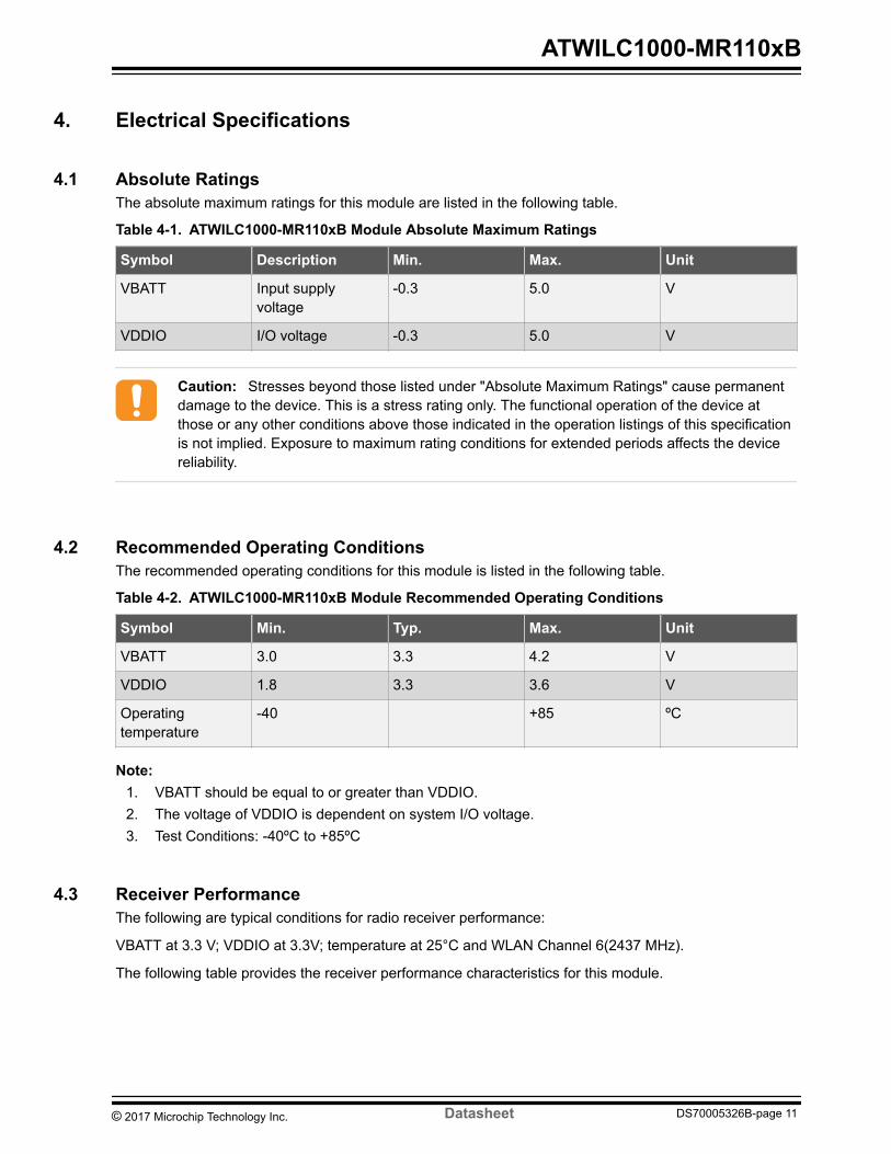
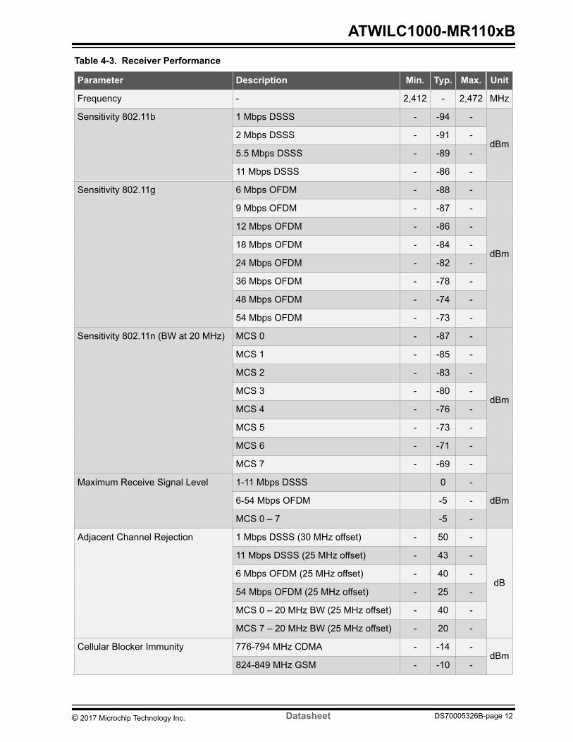
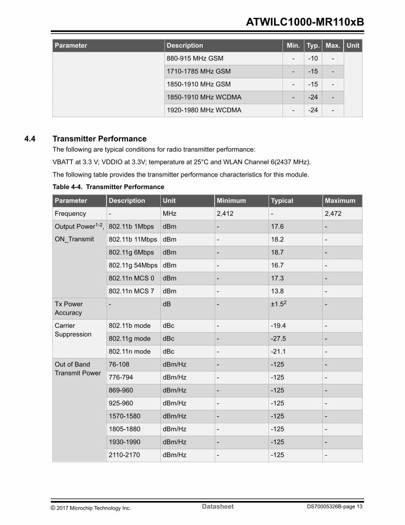
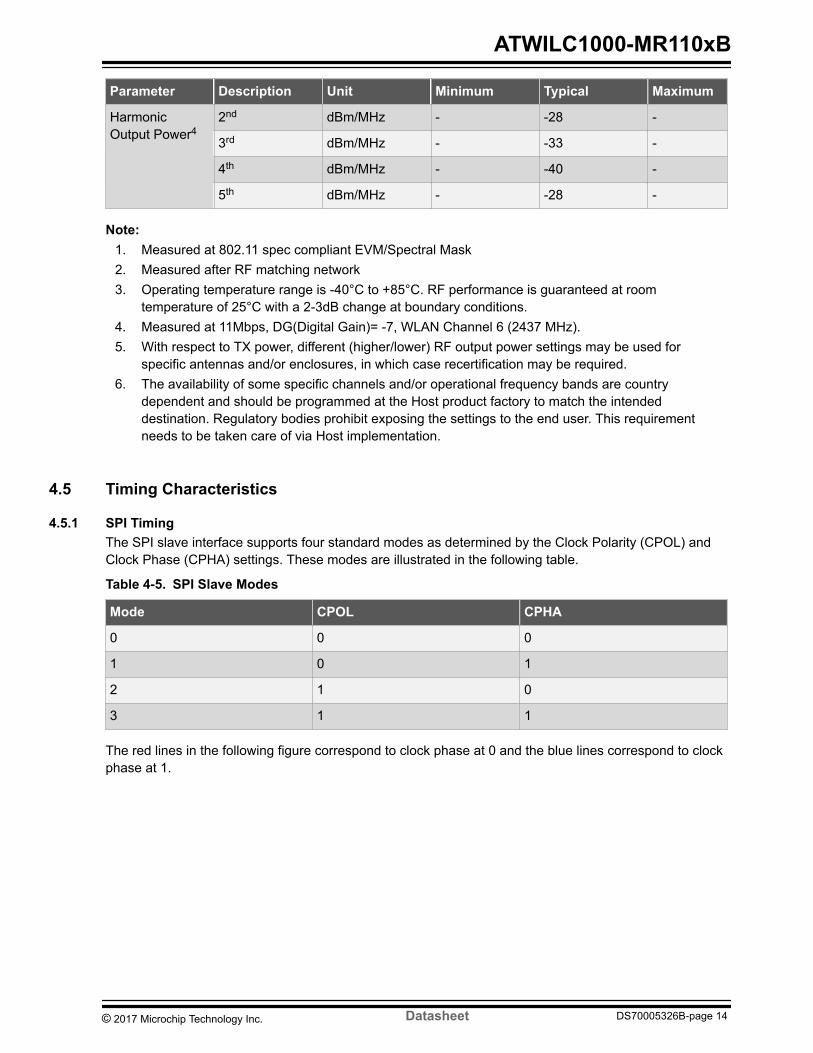
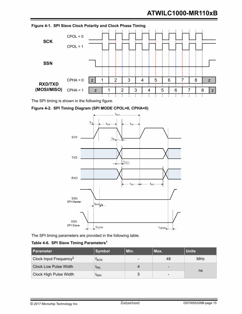

Parameter Symbol Min Max Units
Clock Rise Time tLH 0 7
Clock Fall Time tHL 0 7
TXD Output Delay3 tODLY 4 9 from SCK fall125 from SCKrise
RXD Input Setup Time tISU 1 -
RXD Input Hold Time tIHD 5 -
SSN Input Setup Time tSUSSN 3 -
SSN Input Hold Time tHDSSN 55 -
Note 1 Timing is applicable to all SPI modes2 Maximum clock frequency specified is limited by the SPI slave interface internal design actual
maximum clock frequency can be lower and depends on the specific PCB layout3 Timing is based on 15pF output loading
452 SDIO TimingThe SDIO Slave interface timing is shown in following figure
Figure 4-3 SDIO Timing Diagram
Slave timing parameters are provided in the following tableTable 4-7 SDIO Timing Parameters
Parameter Symbol Min Max Units
Clock InputFrequency1
fPP 0 50 MHz
Clock Low PulseWidth
tWL 9 - ns
ATWILC1000-MR110xB
copy 2017 Microchip Technology Inc Datasheet DS70005326B-page 16
Parameter Symbol Min Max Units
Clock High PulseWidth
tWH 45 -
Clock Rise Time tLH 0 5
Clock Fall Time tHL 0 5
Input Setup Time tISU 6 -
Input Hold Time tIH 4 -
Output Delay2 tODLY 3 11
1 Maximum clock frequency specified is limited by the SDIO Slave interface internal design actualmaximum clock frequency can be lower and depends on the specific PCB layout
2 Timing based on 15pF output loading
453 I2C TimingThe following figure illustrates I2C Slave timing
Figure 4-4 I2C Timing Diagram
The following table provides I2C Slave timing parameters
Table 4-8 I2C Timing Parameters
Parameter Symbol Min Max Units Remarks
SCL ClockFrequency
fSCL 0 400 kHZ -
SCL Low PulseWidth
tWL 13 - micros -
SCL High PulseWidth
tWH 06 - micros -
SCL SDA FallTime
tHL - 300 ns -
ATWILC1000-MR110xB
copy 2017 Microchip Technology Inc Datasheet DS70005326B-page 17
Parameter Symbol Min Max Units Remarks
SCL SDA RiseTime
tLH - 300 ns This is dictatedby externalcomponents
START SetupTime
tSUSTA 06 - micros -
START HoldTime
tHDSTA 06 - micros -
SDA SetupTime
tSUDAT 100 - ns -
SDA Hold Time tHDDAT 0 - ns Slave andMaster Default
MasterProgrammingOption
40 - ns
STOP Setuptime
tSUSTO 06 - micros -
Bus Free TimeBetween STOPand START
tBUF 13 - micros -
Glitch PulseReject
tPR 0 50 ns -
ATWILC1000-MR110xB
copy 2017 Microchip Technology Inc Datasheet DS70005326B-page 18
5 Power ManagementThe ATWILC1000-MR110xB module has several device states
bull On statesndash ON_Transmit ndash device actively transmits an 80211 signal Highest output power and nominal
current consumptionndash ON_Receive ndash device actively receivies an 80211 signal Lowest sensitivity and nominal
current consumptionndash ON_Doze ndash device is powered on but it does not actively transmit or receive the datandash Power_Down ndash device core supply is powered off
The following pins are used to switch between the ON and Power_Down statesbull CHIP_EN ndash this pin (pin 22) enables or disables the DCDC converterbull VDDIO ndash IO supply voltage from external supply
In the ON states VDDIO is ON and CHIP_EN is high (at VDDIO voltage level) To change from the ONstates to Power_Down state connect the RESETN and CHIP_EN pin to logic low (GND) by following thepower down sequence mentioned in Power-UpDown Sequence When VDDIO is off and CHIP_EN islow the chip is powered off with no leakage (also see Restrictions for Power States)
51 Current Consumption in Various Device StatesThe following table provides this modules current consumption in various device states
Table 5-1 Current Consumption
Device State Code Rate Output
Power (dBm)
Current Consumption1
IVBATT IVDDIO
ON_Transmit 80211b 1Mbps 176 266 mA 22 mA
80211b 11Mbps 185 239 mA 22 mA
80211g 6Mbps 186 249 mA 22 mA
80211g 54Mbps 169 173 mA 22 mA
80211n MCS 0 177 253 mA 22 mA
80211n MCS 7 140 164 mA 22 mA
ON_Receive 80211b 1Mbps NA 63 mA 22 mA
80211b 11Mbps NA 63 mA 22 mA
80211g 6Mbps NA 63 mA 22 mA
80211g 54Mbps NA 63 mA 22 mA
80211n MCS 0 NA 63 mA 22 mA
80211n MCS 7 NA 63 mA 22 mA
ATWILC1000-MR110xB
copy 2017 Microchip Technology Inc Datasheet DS70005326B-page 19
Device State Code Rate Output
Power (dBm)
Current Consumption1
ON_Doze NA NA 380microA lt10microA
Power_Down NA NA 125 uA(2)
Note 1 The power consumption values are measured when VBAT is 33V and VDDIO is 33V at 25degC2 Current consumption mentioned for these states is the sum of current consumed in VDDIO and
VBAT voltage rails
52 Restrictions for Power StatesWhen no power is supplied to the device the DCDC Converter output and VDDIO are both turned off (atground potential) In this case a voltage cannot be applied to the device pins because each pin containsan ESD diode from the pin to supply This diode will turn on when voltage higher than one diode-drop issupplied to the pin
If a voltage must be applied to the signal pads while the chip is in a low power state the VDDIO supplymust be on so the Sleep mode or power-down state must be used
Similarly to prevent the pin-to-ground diode from turning on do not apply a voltage that is more than onediode-drop below ground to any pin
53 Power-UpDown SequenceThe following figure illustrates the power-updown sequence for the ATWILC1000-MR110xB module
Figure 5-1 Power-UpDown Sequence
The following table provides power-updown sequence timing parameters
ATWILC1000-MR110xB
copy 2017 Microchip Technology Inc Datasheet DS70005326B-page 20
Table 5-2 Power-UpDown Sequence Timing
Parameter Min Max Units Description Notes
tA 0 - ms VBAT rise toVDDIO rise
VBAT and VDDIO can risesimultaneously or connected togetherVDDIO must not rise before VBAT
tB 0 - ms VDDIO rise toCHIP_EN rise
CHIP_EN must not rise before VDDIOCHIP_EN must be driven high or lowand must not be left floating
tC 5 - ms CHIP_EN rise toRESETN rise
This delay is required to stabilize the XOclock before RESETN removal RESETNmust be driven high or low and must notbe left floating
tArsquo 0 - ms VDDIO fall toVBAT fall
VBAT and VDDIO fall simultaneously orconnected together VBAT must not fallbefore VDDIO
tBrsquo 0 - ms CHIP_EN fall toVDDIO fall
VDDIO must not fall before CHIP_ENCHIP_EN and RESETN must fallsimultaneously
tCrsquo 0 - ms RESETN fall toVDDIO fall
VDDIO must not fall before RESETNRESETN and CHIP_EN fallsimultaneously
54 Digital IO Pin Behavior During Power-Up SequencesThe following table represents the digital IO pin states corresponding to the device power modes
Table 5-3 Digital IO Pin Behavior in Different Device States
Device State VDDIO CHIP_EN RESETN Output Driver InputDriver
Pull UpDownResistor (96
kOhm)
Power_Down coresupply OFF
High Low Low Disabled (Hi-Z) Disabled Disabled
Power-On Resetcore supply and hardreset ON
High High Low Disabled (Hi-Z) Disabled Enabled
Power-On Defaultcore supply ONdevice out of resetand not programmed
High High High Disabled (Hi-Z) Enabled Enabled
On_Doze
On_Transmit
High High High Programmedby firmware foreach pinenabled ordisabled
Oppositeof OutputDriverstate
Programmedby firmware foreach pinenabled ordisabled
ATWILC1000-MR110xB
copy 2017 Microchip Technology Inc Datasheet DS70005326B-page 21
Device State VDDIO CHIP_EN RESETN Output Driver InputDriver
Pull UpDownResistor (96
kOhm)
On_Receive coresupply ON deviceprogrammed byfirmware
ATWILC1000-MR110xB
copy 2017 Microchip Technology Inc Datasheet DS70005326B-page 22
6 CPU and Memory Subsystems
61 ProcessorThis ATWILC1000-MR110xB module has a Cortus APS3 32-bit processor This processor performs manyof the MAC functions including but not limited to association authentication power management securitykey management and MSDU aggregationdeaggregation In addition the processor provides flexibility forvarious modes of operation such as STA and AP modes
62 Memory SubsystemThe APS3 core uses a 128 KB instructionboot ROM along with a 160 KB instruction RAM and a 64 KBdata RAM In addition the device uses a 128 KB shared RAM accessible by the processor and MAC thatallows the APS3 core to perform various data management tasks on the Tx and Rx data packets
63 Nonvolatile Memory (eFuse)This ATWILC1000-MR110xB module has 768 bits of nonvolatile eFuse memory that is read by the CPUafter device reset This nonvolatile One-Time-Programmable (OTP) memory is used to store customerspecific parameters such as MAC address various calibration information such as Tx power crystalfrequency offset etc and other software-specific configuration parameters The eFuse is partitioned intosix 128 bit banks Each bank has the same bit map mentioned in the following figure The purpose of thefirst 80 bits in each bank is fixed and the remaining 48 bits are general purpose software dependent bitsEach bank is programmed independently which allows for several updates of the device parametersfollowing the initial programming For example if the MAC address has to be changed Bank 1 has to beprogrammed with the new MAC address along with the values of TX gain correction and Frequency offsetif they are used and programmed in the Bank 0 The contents of Bank 0 have to be invalidated in thiscase by programming the Invalid bit in the Bank 0 This will allow the firmware to use the MAC addressfrom Bank 1
By default all the ATWILC1000-MR110PB and ATWILC1000-MR110UB modules are programmed withthe MAC address and the Frequency offset bits of Bank 0
ATWILC1000-MR110xB
copy 2017 Microchip Technology Inc Datasheet DS70005326B-page 23
Figure 6-1 eFuse Bit Map
ATWILC1000-MR110xB
copy 2017 Microchip Technology Inc Datasheet DS70005326B-page 24
7 WLAN SubsystemThe WLAN subsystem is composed of the Media Access Controller (MAC) Physical Layer (PHY) andthe radio
71 MAC
711 DescriptionThis module is designed to operate at low power while providing high data throughput The IEEE 80211MAC functions are implemented with a combination of dedicated datapath engines hardwired controllogic and a low power high-efficiency microprocessor The combination of dedicated logic with aprogrammable processor provides optimal power efficiency and real time response while providing theflexibility to accommodate evolving standards and future feature enhancements
The dedicated datapath engines are used to implement data path functions with heavy computationalrequirements For example a Frame Check Sequence (FCS) engine checks the Cyclic RedundancyCheck (CRC) of the transmitting and receiving packets and a cipher engine performs all the requiredencryption and decryption operations for the WEP WPA-TKIP WPA2 CCMP-AES and WPA2 Enterprisesecurity requirements
Control functions which have real time requirements are implemented using hardwired control logicmodules These logic modules offer real time response while maintaining configurability through theprocessor Examples of hardwired control logic modules are the channel access control module(implements EDCAHCCA Beacon Tx control interframe spacing and so on) protocol timer module(responsible for the Network Access vector back-off timing timing synchronization function and slotmanagement) MAC Protocol Data Unit (MPDU) handling module aggregationdeaggregation moduleblock ACK controller (implements the protocol requirements for burst block communication) and TxRxcontrol Finite State Machine (FSM) (coordinate data movement between PHY and MAC interface cipherengine and the Direct Memory Acces (DMA) interface to the TxRx FIFOs)
Following are the characteristics of MAC functions implemented solely in software on the microprocessor
bull Functions with high memory requirements or complex data structures Examples are associationtable management and power save queuing
bull Functions with low computational load or without critical real time requirements Examples areauthentication and association
bull Functions that require flexibility and upgradeability Examples are beacon frame processing andQoS scheduling
712 FeaturesThe ATWILC1000-MR110xB IEEE 80211 MAC supports the following functions
bull IEEE 80211bgnbull IEEE 80211e WMM QoS EDCAPCF multiple access categories traffic schedulingbull Advanced IEEE 80211n features
ndash Transmission and reception of aggregated MPDUs (A-MPDU)ndash Transmission and reception of aggregated MSDUs (A-MSDU)ndash Immediate block acknowledgmentndash Reduced Interframe Spacing (RIFS)
bull Supports IEEE 80211i and WFA security with key management
ATWILC1000-MR110xB
copy 2017 Microchip Technology Inc Datasheet DS70005326B-page 25
ndash WEP 64128ndash WPA-TKIPndash 128-bit WPA2 CCMP (AES)ndash WPA2 Enterprise
bull Advanced power managementndash Standard IEEE 80211 Power save modendash Wi-Fi alliance WMM-PS (U-APSD)
bull RTS-CTS and CTS self supportbull Supports either STA or AP mode in the infrastructure basic service set modebull Supports concurrent mode of operationbull Supports Independent Basic Service Set (IBSS)
72 PHYThe ATWILC1000-MR110xB module WLAN PHY is designed to achieve reliable and power-efficientphysical layer communication specified by IEEE 80211 bgn in single stream mode with 20 MHzbandwidth The advanced algorithms are used to achieve maximum throughput in a real worldcommunication environment with impairments and interference The PHY implements all the requiredfunctions such as Fast Fourier Transform (FFT) filtering Forward Error Correction (FEC) that is a Viterbidecoder frequency timing acquisition and tracking channel estimation and equalization carrier sensingclear channel assessment and automatic gain control
Features
The IEEE 80211 PHY supports the following functions
bull Single antenna 1x1 stream in 20 MHz channelsbull Supports IEEE 80211b DSSS-CCK modulation 1 2 55 and 11 Mbpsbull Supports IEEE 80211g OFDM modulation 6 9 1218 24 36 48 and 54 Mbpsbull Supports IEEE 80211n HT modulations MCS0-7 20 MHz 800 and 400ns guard interval 65 72
130 144 195 217 260 289 390 433 520 578 585 650 and 722 Mbpsbull IEEE 80211n mixed mode operationbull Per packet Tx power controlbull Advanced channel estimationequalization automatic gain control CCA carriersymbol recovery
and frame detection
721 FeaturesThe IEEE 80211 PHY supports the following functions
bull Single antenna 1x1 stream in 20 MHz channelsbull Supports IEEE 80211b DSSS-CCK modulation 1 2 55 and 11 Mbpsbull Supports IEEE 80211g OFDM modulation 6 9 1218 24 36 48 and 54 Mbpsbull Supports IEEE 80211n HT modulations MCS0-7 20 MHz 800 and 400ns guard interval 65 72
130 144 195 217 260 289 390 433 520 578 585 650 and 722 Mbpsbull IEEE 80211n mixed mode operationbull Per packet Tx power controlbull Advanced channel estimationequalization automatic gain control CCA carriersymbol recovery
and frame detection
ATWILC1000-MR110xB
copy 2017 Microchip Technology Inc Datasheet DS70005326B-page 26
73 RadioThis section describes the properties and characteristics of the ATWILC1000- MR110xB and Wi-Fi radiotransmit and receive performance capabilities of the device The performance measurements are taken atthe RF pin assuming 50Ω impedance the RF performance is guaranteed for room temperature of 25degCwith a derating of 2-3dB at boundary conditions
Measurements were taken under typical conditions VBATT at 33V VDDIO at 33V and temperature at+25ordmC
Table 7-1 Features and Properties
Feature Description
Module Part Number ATWILC1000-MR110xB
WLAN Standard IEEE 80211bgn Wi-Fi compliant
Host Interface SPI SDIO
Dimension L x W x H 217 x 147 x 21 (typical) mm
Frequency range 2412 GHz ~ 2472 GHz (24 GHz ISM band)
Number of channels 11 for North America 13 for Europe
Modulation 80211b DQPSK DBPSK CCK
80211gn OFDM64-QAM16-QAM QPSK BPSK
Data rate 80211b 1 2 55 11 Mbps80211g 6 9 12 18 24 36 48 54 Mbps
Data rate
(20 MHz short GI400ns)
80211n 72 144 217 289 433 578 65722Mbps
Operating temperature(1) -40degC to 85degC
Storage temperature -40degC to 125degC
Humidity Operating humidity 10 to 95 non-condensing
Storage humidity 5 to 95 non-condensing
Note 1 RF performance is guaranteed at room temperature of 25degC with a 2-3db change at boundary
conditions
ATWILC1000-MR110xB
copy 2017 Microchip Technology Inc Datasheet DS70005326B-page 27
8 External InterfacesThis section describes the various host and debug interfaces of the ATWILC1000-MR110xB module
81 Interfacing with the Host MicrocontrollerThis section describes how to interface ATWILC1000-MR110xB module with the host microcontroller Theinterface comprises of a slave SPISDIO and additional control signals as shown in the figure Additionalcontrol signals are connected to the GPIOIRQ interface of the microcontroller
Figure 8-1 Interfacing with the Host Microcontroller
Table 8-1 Host Microcontroller Interface Pins
Module Pin Function(1)
4 RESET_N
11 WAKE
13 IRQ_N
22 CHIP_EN
16 SPI_SSNSD_DATA1
15 SPI_MOSISD_DATA2
17 SPI_MISOSD_DATA0
18 SPI_SCKSD_CMD
ATWILC1000-MR110xB
copy 2017 Microchip Technology Inc Datasheet DS70005326B-page 28
Module Pin Function(1)
14 SD_DATA3
19 SD_CLK
Note 1 Logic input for module pin SDIO_SPI_CFG(10) determines whether SDIO or SPI slave interface is
enabled Connect SDIO_SPI_CFG to VDDIO through a 1MΩ resistor to enable the SPI interfaceConnect SDIO_SPI_CFG to ground to enable SDIO interface
2 It is recommended to place test points for pins I2C_SDA(3) I2C_SCL(2) GPIO_3(25) andGPIO_5(27) in the design
82 SPI Slave InterfaceThe SPI slave interface can be enabled by connecting the SDIO_SPI_CFG pin to VDDIO This SPIinterface is used to exchange the control and 80211 data The SPI is a full duplex slave-synchronousserial interface that is available following reset when pin 10 (SDIO_SPI_CFG) is connected to VDDIO
The SPI interface pin mapping configuration is provided in the following table
Table 8-2 SPI Interface Pin Mapping
Pin SPI Function
10 SDIO_SPI_CFG Must be connected to VDDIO
16 SSN Active-Low Slave Select
15 MOSI Serial Data Receive
18 SCK Serial Clock
17 MISO Serial Data Transmit
When the SPI is not selected ie when SSN is high the SPI interface will not interfere with datatransfers between the serial master and other serial slave devices When the serial slave is not selectedits transmitted data output is buffered resulting in a high impedance drive onto the MISO line
The SPI interface responds to a protocol that allows an external host to read or write any register in thechip and also initiate DMA transfers
The SPI SSN MOSI MISO and SCK pins of this module have internal programmable pull up resistorsThese resistors are programmed to be disabled Otherwise if any of the SPI pins are driven to a low levelwhile this module is in the low power sleep state current will flow from the VDDIO supply through the pullup resistors increasing the current consumption of the module
83 SDIO Slave InterfaceThe SDIO interface is enabled by connecting the SDIO_SPI_CFG pin to ground This SDIO interface isused to exchange the control and 80211 data The SDIO interface is available after reset when pin 10(SDIO_SPI_CFG) is connected to ground
This SDIO is a full speed interface The interface supports the 1-bit4-bit SD transfer mode at the clockrange of 0-50 MHz The host uses this interface to read and write from any register within the chip andalso configures this module for DMA data transfer
ATWILC1000-MR110xB
copy 2017 Microchip Technology Inc Datasheet DS70005326B-page 29
The SDIO interface pin mapping configuration is provided in the following table
Table 8-3 ATWILC1000 SDIO Interface Pin Mapping
Pin SDIO Function
10 SDIO_SPI_CFG Must be connected to ground
14 DAT3 Data 3
15 DAT2 Data 2
16 DAT1 Data 1
17 DAT0 Data 0
18 CMD Command
19 CLK Clock
The SDIO card is detected when the it is inserted into an SDIO host During the normal initialization andinterrogation of the card by the host the card identifies itself as an SDIO device The host softwareobtains the card information in a tuple (linked list) format and determines if that cardrsquos IO function(s) areacceptable to activate If the card is acceptable it is allowed to power-up fully and start the IO function(s)built into the card
The SD memory card communication is based on an advanced 9-pin interface (clock command fourdata and three power lines) designed to operate at maximum operating frequency of 50 MHz
831 Featuresbull Compliant with SDIO card specification version 20bull Host clock rate variable between 0 and 50 MHzbull Supports 1-bit4-bit SD bus modesbull Allows card to interrupt hostbull Responds to direct readwrite (IO52) and extended readwrite (IO53) transactionsbull Supports suspendresume operation
84 UART Debug InterfaceThis module has a Universal Asynchronous ReceiverTransmitter (UART) interface on J25(RxD) andJ27(TxD) pins This interface should be used only for debugging purposes The UART is compatible withthe RS-232 standard where ATWILC1000-MR110xB operates as Data Terminal Equipment (DTE) It hasa two-pin RXDTXD interface
The default configuration for accessing the UART interface of ATWILC1000-MR110xB is mentionedbelow
bull Baud rate 115200bull Data 8 bitbull Parity Nonebull Stop bit 1 bitbull Flow control None
It also has Rx and Tx FIFOs which ensures reliable high speed reception and low software overheadtransmission FIFO size is 4x8 for both Rx and Tx direction The UART has status registers that show the
ATWILC1000-MR110xB
copy 2017 Microchip Technology Inc Datasheet DS70005326B-page 30
number of received characters available in the FIFO and various error conditions in addition it has theability to generate interrupts based on these status bits
An example of UART receiving or transmitting a single packet is shown in the following figure Thisexample shows 7-bit data (0x45) odd parity and two stop bits
Figure 8-2 Example of UART RX or TX Packet
85 I2C Slave InterfaceThis module provides an I2C bus slave that allows for easy debugging of the ATWILC1000-MR110xBdevices It supports I2C bus Version 21 ndash 2000
The I2C interface is used only for debug This interface is a two-wire serial interface consisting of a serialdata line (SDA Pin 17) and a serial clock (SCL Pin 18) It responds to seven bit address value 0x60This module I2C interface operates in standard mode (with data rates up to 100Kbs) and fast mode (withdata rates up to 400Kbs)
The I2C is a synchronous serial interface The SDA line is a bidirectional signal and changes only whenthe SCL line is low except for STOP START and RESTART conditions The output drivers are open-drain to perform wire AND functions on the bus The devices on the bus are limited to the 400pFcapacitance Data is transmitted in byte packages
For specific information refer to the Philips Specification entitled ldquoThe I2C -Bus Specification Version21rdquo
ATWILC1000-MR110xB
copy 2017 Microchip Technology Inc Datasheet DS70005326B-page 31
9 Notes on Interfacing with the ATWILC1000-MR110xBProgrammable Pull up Resistors
The ATWILC1000-MR110xB module provides programmable pull up resistors on various pins Thepurpose of these resistors is to keep any unused input pins from floating which causes excess current toflow through the input buffer from the VDDIO supply Any unused pin on the device must leave these pullup resistors enabled so that the pin will not float The default state at power-up is for the pull up resistorto be enabled however any pin that is used must have the pull up resistor disabled The reason for thisis that if any pins are driven to a low level while the device is in the low power sleep state current flowsfrom the VDDIO supply through the pull up resistors increasing the current consumption of the moduleSince the value of the pull up resistor is approximately 100 kOhm the current through any pull up resistorthat is being driven low is VDDIO100K For VDDIO = 33V the current is approximately 33 microA The pinsthat are used and have programmable the pull up resistor disabled should always be actively driven toeither a high or low level and not be allowed to float
ATWILC1000-MR110xB
copy 2017 Microchip Technology Inc Datasheet DS70005326B-page 32
10 Application Reference DesignThis section provides reference schematic for ATWILC1000-MR110xB module with SPI and SDIO hostinterfacesFigure 10-1 ATWILC1000-MR110xB Reference Schetmatic - SDIO Host Interface
Table 10-1 ATWILC1000-MR110xB reference Schematic - SDIO Host Interface - Bill of Materials
Item Qty Reference Value Description
Manufacturer
PartNumber
Footprint
1 9 R2 R3R4R5 R6R7 R8R9 R10
0 R RESISTORThick Film0 ohm0402
Yageo RC0402JR-070RL
0402
2 1 U1 ATWILC1000-MR110xB
Wi-FiModule
Microchip ATWILC1000-MR110xB
ATWILC1000-MR110xB
copy 2017 Microchip Technology Inc Datasheet DS70005326B-page 33
Figure 10-2 ATWILC1000-MR110xB Reference Schetmatic - SPI Host Interface
Table 10-2 ATWILC1000-MR110xB reference Schematic - SPI Host Interface - Bill of Materials
Item Qty Reference Value Description
Manufacturer
PartNumber
Footprint
1 1 R1 1 M RESISTORThick Film1 M ohm0402
Yageo RC0100FR-071ML
0402
2 9 R2 R3R4R5 R6R7 R8R9 R10
0 R RESISTORThick Film0 ohm0402
Yageo RC0402JR-070RL
0402
3 1 U1 ATWILC1000-MR110xB
Wi-FiModule
Microchip ATWILC1000-MR110xB
ATWILC1000-MR110xB
copy 2017 Microchip Technology Inc Datasheet DS70005326B-page 34
11 Module Outline DrawingsThe ATWILC1000-MR110PB module package details are outlined in the following figure Dimensions arein mm
Figure 11-1 Module Drawings ndash ATWILC1000-MR110PB - Top Bottom and Side Views
MODULE TOP VIEW
Metal Shield
Metal Shield
PCB
MODULE SIDE VIEW MODULE BOTTOM VIEW
NOTE THIS PAD MUST BE SOLDERED TO GND
NOT TO SCALE
The ATWILC1000-MR110UB module package details are outlined in the following figure Dimensions arein mm
ATWILC1000-MR110xB
copy 2017 Microchip Technology Inc Datasheet DS70005326B-page 35
Figure 11-2 Module Drawings ndash ATWILC1000-MR110UB - Top Bottom and Side Views
MODULE TOP VIEW
Metal Shield
Metal Shield
PCB
MODULE SIDE VIEW MODULE BOTTOM VIEW
NOTE THIS PAD MUST BE SOLDERED TO GND
NOT TO SCALE Rev 2
This section provides the outline drawing for the recommended footprint for the ATWILC1000-MR110xBmodule It is imperative that the center Ground Pad is provided with an array of GND vias to provide agood ground and act as thermal sink for the ATWILC1000-MR110xB module
ATWILC1000-MR110xB
copy 2017 Microchip Technology Inc Datasheet DS70005326B-page 36
Figure 11-3 Recommended Solder Pad Footprint
NOTE THIS PAD MUST BE TIED TO GND
1016 Pitch
1473
19
08
1016 Pitch
4064
267
267
600
1016 Pitch
370
370
1016 Pitch
19 3048
368
2172 2032
442
SOLDER PAD FOOTPRINT
Drawing not to scaleUntoleranced dimensionsUnits=mm
ATWILC1000-MR110xB
copy 2017 Microchip Technology Inc Datasheet DS70005326B-page 37
12 Design ConsiderationThis section provides the guidelines on placement and routing to achieve the best performance
121 ATWILC1000-MR110PB Placement and Routing GuidelinesIt is critical to follow the recommendations listed below to achieve the best RF performance
bull The module must be placed on host board The printed antenna area must overlap with the carrierboard The portion of the module containing the antenna should not stick out over the edge of thehost board The antenna is designed to work properly when it is sitting directly on top of a 15mmthick printed circuit board Figure 12-2 shows the best poor and worst case module placements inhost board
bull If the module is placed at the edge of the host board a minimum 22mm by 5 mm area directlyunder the antenna must be clear of all metal on all layers of the board ldquoIn-landrdquo placement isacceptable however deepness of keep-out area must grove to module edge to host board edgeplus 5 mmNote Do not place the module in the middle of the host board or far away from the host boardedge
bull Follow the module placement keepout host PCB cutout recommendation as shown in Figure 12-1ndash Avoid routing any traces in the highlighted region on the top layer of the host board which will
be directly below the module areandash Follow the electrical keepout layer recommendation as shown in Figure 12-1 There should be
no copper in all layers of the host board in this region Avoid placing any components (likemechanical spacers bumpon etc) in the recommended electrical keepout area
ndash Place GND polygon pour below the module with the recommended boundary in the top layerof the host board as shown in Figure 12-1 Do not have any breaks in this GND plane
ndash Place sufficient GND vias in the highlighted area below the module for better RFperformance
ndash It is recommended to have a 3x3 grid of GND vias solidly connecting the exposed GNDpaddle of the module to the inner layer ground plane This will act as a good ground andthermal conduction for the ATWILC1000-MR110PB module The GND vias should have aminimum via hole size of 03mm
ndash Follow the mechanical boundary of the host PCB as shown in the Figure 12-1bull Keep the large metal objects away from antenna to avoid electromagnetic field blockingbull Do not enclose the antenna within a metal shieldbull Keep any components which may radiate noise or signals within the 24 GHz ndash 25 GHz frequency
band away from the antenna and if possible shield those components Any noise radiated from thehost board in this frequency band will degrade the sensitivity of the module
bull Make sure the width of the traces routed to GND VDDIO and VBAT rails are sufficiently larger forhandling the peak Tx current consumption
ATWILC1000-MR110xB
copy 2017 Microchip Technology Inc Datasheet DS70005326B-page 38
Figure 12-1 ATWILC1000-MR110PB Placement Reference
Figure 12-2 ATWILC1000-MR110PB Placement Example
122 Printed PCB Antenna Performance of ATWILC1000-MR110PBThe printed PCB antenna on the ATWILC1000-MR110PB is a meandered Inverted F Antenna (IFA) Theantenna is fed via matching network which is matched for the module installed on 15mm thick mainboard Main board thickness deviation by plusmn1mm changes RXTX performance by plusmn1dB maximumreferring to RXTX performance with default antenna matching network and installed on 15mm thick mainboard
Measured antenna gain is -03dBi
ATWILC1000-MR110xB
copy 2017 Microchip Technology Inc Datasheet DS70005326B-page 39
Antenna Radiation PatternFollowing figures illustrate the antenna radiation pattern During the measurement the printed antenna isplaced in the XZ plane with Y axis being perpendicular to the module and pointing to the back of themoduleFigure 12-3 Antenna Radiation Pattern when Phi = 0 degree
Figure 12-4 Antenna Radiation Pattern when Phi = 90 degree
ATWILC1000-MR110xB
copy 2017 Microchip Technology Inc Datasheet DS70005326B-page 40
Figure 12-5 Antenna Radiation Pattern when Theta = 90 degree
ATWILC1000-MR110xB
copy 2017 Microchip Technology Inc Datasheet DS70005326B-page 41
123 ATWILC1000-MR110UB Placement and Routing GuidelinesThe ATWILC1000-MR110UB module has an Ultra Small Miniature RF Connector (uFL) for the externalantenna
The choice of antenna is limited to the antenna types for which the module was tested and approved Fora list of tested and approved antennas that may be used with the module refer to the respective countryin the Regulatory Approval section
An approved and tested antenna type is shown in the following Table
Table 12-1 Tested External Antenna Type
Antenna Type Gain
PCB Antenna 20 dBi
ATWILC1000-MR110xB
copy 2017 Microchip Technology Inc Datasheet DS70005326B-page 42
1231 Recommended External Antenna for ATWILC1000-MR110UBPCB Antenna (Part number W3525B039) along with a 10cm length RF cable assembly (uFL to SMA)has been used for the certification of ATWILC1000-MR110UB It is recommended to use the same orsimilar external antenna in design
ATWILC1000-MR110xB
copy 2017 Microchip Technology Inc Datasheet DS70005326B-page 43
13 Reflow Profile InformationThis section provides the guidelines for the reflow process to get the module soldered to the customersdesign
131 Storage Condition
1311 Moisture Barrier Bag Before OpeningA moisture barrier bag must be stored in a temperature of less than 30degC with humidity under 85 RHThe calculated shelf life for the dry-packed product shall be 12 months from the date the bag is sealed
1312 Moisture Barrier Bag OpenHumidity indicator cards must be blue indicating that the humidity is lt30
132 Solder PasteSnAgCu eutectic solder with melting temperature of 217degC is most commonly used for lead-free solderreflow application This alloy is widely accepted in the semiconductor industry due to its low costrelatively low melting temperature and good thermal fatigue resistance Some recommended pastesinclude NC-SMQreg 230 flux and Indalloyreg 241 solder paste made up of 955 Sn38 Ag07 Cu or SENJUN705-GRN3360-K2-V Type 3 no clean paste
133 Stencil DesignThe recommended stencil is laser-cut stainless-steel type with thickness of 100 microm to 130 microm andapproximately a 11 ratio of stencil opening to pad dimension To improve paste release a positive taperwith bottom opening 25 microm larger than the top is utilized Local manufacturing experience may find othercombinations of stencil thickness and aperture size to get good results
134 Printing ProcessThe printing process requires no significant changes compared to SnPb solder Any guidelinesrecommended by the paste manufacturers to accommodate paste specific characteristics should befollowed Post-print inspection and paste volume measurement is very critical to ensure good print qualityand uniform paste
135 Baking ConditionsThis module is rated at MSL level 3 After the sealed bag is opened no baking is required within 168hours as long as the devices are held at le 30degC60 RH or stored at lt 10 RH
The module requires baking before mounting ifbull The sealed bag has been open for more than 168 hoursbull The humidity indicator card reads more than 10bull SIPs need to be baked for eight hours at 125degC
ATWILC1000-MR110xB
copy 2017 Microchip Technology Inc Datasheet DS70005326B-page 44
136 Soldering and Reflow ConditionOptimization of the reflow process is the most critical factor considered for lead-free soldering Thedevelopment of an optimal profile must account the paste characteristics the size of the board thedensity of the components the mix of the larger and smaller components and the peak temperaturerequirements of the components An optimized reflow process is the key to ensuring a successful lead-free assembly and achieves high yield and long-term solder joint reliability
Temperature ProfilingTemperature profiling must be performed for all new board designs by attaching thermocouples at thesolder joints on the top surface of the larger components and at multiple locations of the boards This isto ensure that all components are heated to a temperature above the minimum reflow temperatures andthe smaller components do not exceed the maximum temperature limit The SnAgCu solder alloy melts at~217degC so the reflow temperature peak at joint level must be 15 to 20degC higher than meltingtemperature The targeted solder joint temperature for the SnAgCu solder must be ~235degC For larger orsophisticated boards with a large mix of components it is also important to ensure that the temperaturedifference across the board is less than 10 degrees to minimize board warpage The maximumtemperature at the component body must not exceed the MSL3 qualification specification
1361 Reflow OvenIt is strongly recommended that a reflow oven equipped with more heating zones and Nitrogenatmosphere be used for lead-free assembly Nitrogen atmosphere has shown to improve the wet-abilityand reduce temperature gradient across the board It can also enhance the appearance of the solderjoints by reducing the effects of oxidation
The following items should also be observed in the reflow process1 Some recommended pastes include
ndash NC-SMQreg 230 flux and Indalloyreg 241 solder paste made up of 955 Sn38 Ag07 Cundash SENJU N705-GRN3360-K2-V Type 3 no clean paste
2 Allowable reflow soldering iterationsndash Three times based on the following reflow soldering profile (refer following Figure)
3 Temperature profilendash Reflow soldering shall be done according to the following temperature profile (refer to the
following figure)ndash Peak temperature 250degC
ATWILC1000-MR110xB
copy 2017 Microchip Technology Inc Datasheet DS70005326B-page 45
Figure 13-1 Solder Reflow Profile
Cleaning
The exposed ground paddle helps to self-align the module avoiding pad misalignment The use of no-clean solder pastes is recommended Full drying of no-clean paste fluxes must be ensured as a result ofthe reflow process This may require longer reflow profiles andor peak temperatures toward the high endof the process window as recommended by the solder paste vendor It is believed that uncured fluxresidues could lead to corrosion andor shorting in accelerated testing and possibly the field
Rework
Rework is to remove the mounted SIP package and replace with a new unit It is recommended that oncean ATWILC1000-MR110xB module has been removed it should never be reused During the reworkprocess the mounted module and PCB are heated partially and the module is removed It isrecommended to heat-proof the proximity of the mounted parts and junctions and use the best nozzle forrework that is suited to the module size
ATWILC1000-MR110xB
copy 2017 Microchip Technology Inc Datasheet DS70005326B-page 46
14 Module Assembly ConsiderationsThe ATWILC1000-MR110xB modules are assembled with an EMI Shield to ensure compliance with EMIemission and immunity rules The EMI shield is made of a tin-plated steel (SPTE) and is not hermeticallysealed Solutions like IPA and similar solvents can be used to clean the ATWILC1000-MR110xB modulehowever cleaning solutions that contain acid should never be used on the module
The ATWILC1000-MR110xB modules are manufactured without any conformal coating applied It is thecustomerrsquos responsibility if a conformal coating is specified and applied to the ATWILC1000- MR110xBmodule
ATWILC1000-MR110xB
copy 2017 Microchip Technology Inc Datasheet DS70005326B-page 47
15 Regulatory ApprovalRegulatory approvals received
ATWILC1000-MR110PBbull United StatesFCC ID 2ADHKATWILC1000bull CanadaISED
ndash IC 20266-ATWILC1000ndash HVIN ATWILC1000-MR110PB
bull Europe - CE
ATWILC1000-MR110UBbull United StatesFCC ID 2ADHKATWILC1000U
151 United StatesThe ATWILC1000-MR110PB and ATWILC1000-MR110UB modules have received FederalCommunications Commission (FCC) CFR47 Telecommunications Part 15 Subpart C ldquoIntentionalRadiatorsrdquo single-modular approval in accordance with Part 15212 Modular Transmitter approval Single-modular transmitter approval is defined as a complete RF transmission sub-assembly designed to beincorporated into another device that must demonstrate compliance with FCC rules and policiesindependent of any host A transmitter with a modular grant can be installed in different end-use products(referred to as a host host product or host device) by the grantee or other equipment manufacturer thenthe host product may not require additional testing or equipment authorization for the transmitter functionprovided by that specific module or limited module device
The user must comply with all of the instructions provided by the Grantee which indicate installationandor operating conditions necessary for compliance
A host product itself is required to comply with all other applicable FCC equipment authorizationregulations requirements and equipment functions that are not associated with the transmitter moduleportion For example compliance must be demonstrated to regulations for other transmitter componentswithin a host product to requirements for unintentional radiators (Part 15 Subpart B) such as digitaldevices computer peripherals radio receivers etc and to additional authorization requirements for thenon-transmitter functions on the transmitter module (ie Verification or Declaration of Conformity) asappropriate (eg Bluetooth and Wi-Fi transmitter modules may also contain digital logic functions)
1511 Labeling and User Information RequirementsThe ATWILC1000-MR110PB and ATWILC1000-MR110UB modules have been labeled with their ownFCC ID numbers If the FCC ID is not visible when the module is installed inside another device then theoutside of the finished product into which the module is installed must display a label referring to theenclosed module This exterior label can use wording as follows
For the ATWILC1000-MR110PB
Contains Transmitter Module FCC ID 2ADHKATWILC1000 or
Contains FCC ID 2ADHKATWILC1000
This device complies with Part 15 of the FCC Rules Operation is subject to the following twoconditions (1) this device may not cause harmful interference and (2) this device must acceptany interference received including interference that may cause undesired operation
ATWILC1000-MR110xB
copy 2017 Microchip Technology Inc Datasheet DS70005326B-page 48
For the ATWILC1000-MR110UB
Contains Transmitter Module FCC ID 2ADHKATWILC1000U or
Contains FCC ID 2ADHKATWILC1000U
This device complies with Part 15 of the FCC Rules Operation is subject to the following twoconditions (1) this device may not cause harmful interference and (2) this device must acceptany interference received including interference that may cause undesired operation
A users manual for the finished product should include the following statement
This equipment has been tested and found to comply with the limits for a Class B digital devicepursuant to part 15 of the FCC Rules These limits are designed to provide reasonable protectionagainst harmful interference in a residential installation This equipment generates uses and can radiateradio frequency energy and if not installed and used in accordance with the instructions may causeharmful interference to radio communications However there is no guarantee interference will not occurin a particular installation If this equipment does cause harmful interference to radio or televisionreception which can be determined by turning the equipment off and on the user is encouraged to tryto correct the interference by one or more of the following measures
bull Reorient or relocate the receiving antennabull Increase the separation between the equipment and receiverbull Connect the equipment into an outlet on a circuit different from that to which the receiver is
connectedbull Consult the dealer or an experienced radioTV technician for help
Additional information on labeling and user information requirements for Part 15 devices can be found inKDB Publication 784748 which is available at the FCC Office of Engineering and Technology (OET)Laboratory Division Knowledge Database (KDB) httpsappsfccgovoetcfkdbindexcfm
1512 RF ExposureAll transmitters regulated by FCC must comply with RF exposure requirements KDB 447498 General RFExposure Guidance provides guidance in determining whether proposed or existing transmitting facilitiesoperations or devices comply with limits for human exposure to Radio Frequency (RF) fields adopted bythe Federal Communications Commission (FCC)
From the FCC Grant Output power listed is conducted This transmitter is restricted for use with thespecific antenna(s) tested in this application for Certification
In the end product the antenna(s) used with this transmitter must be installed to provide a separationdistance of at least 65 cm from all persons and must not be co-located or operation in conjunction withany other antenna or transmitter User and installers must be provided with antenna installationinstructions and transmitter operating conditions for satisfying the RF exposure compliance
1513 Approved Antenna TypesTo maintain modular approval in the United States only the antenna types that have been tested shall beused It is permissible to use a different antenna provided the same antenna type and antenna gain(equal to or less than) is used An antenna type comprises antennas having similar in-band and out-of-band radiation patterns
Testing the ATWILC1000-MR110UB module was performed with the antenna types listed in Table 12-1
ATWILC1000-MR110xB
copy 2017 Microchip Technology Inc Datasheet DS70005326B-page 49
1514 Helpful WebsitesFederal Communications Commission (FCC) httpwwwfccgov
FCC Office of Engineering and Technology (OET) Laboratory Division Knowledge Database (KDB) httpsappsfccgovoetcfkdbindexcfm
152 CanadaThe ATWILC1000-MR110PB module has been certified for use in Canada under Innova- tion Scienceand Economic Development Canada (ISED formerly Industry Canada) Radio Standards Procedure(RSP) RSP-100 Radio Standards Specifi- cation (RSS) RSS-Gen and RSS-247 Modular approvalpermits the installation of a module in a host device without the need to recertify the device
1521 Labeling and User Information RequirementsLabel Requirements (from RSP-100 Issue 11 Section 3) The host device shall be properly labeled toidentify the module within the host device
The Innovation Science and Economic Development Canada certification label of a module shall beclearly visible at all times when installed in the host device otherwise the host device must be labeled todisplay the Innovation Science and Economic Development Canada certification number of the modulepreceded by the words ldquoContainsrdquo or similar wording expressing the same meaning as follows
For the ATWILC1000-MR110PB
Contains IC 20266-ATWILC1000
User Manual Notice for License-Exempt Radio Apparatus (from Section 84 RSS-Gen Issue 4November 2014) User manuals for license-exempt radio apparatus shall contain the following orequivalent notice in a conspicuous location in the user manual or alternatively on the device or both
This device complies with Industry Canada license exempt RSS standard(s) Operation issubject to the following two conditions
(1) This device may not cause interference and
(2) This device must accept any interference including interference that may cause undesiredoperation of the device
Le preacutesent appareil est conforme aux CNR dIndustrie Canada applicables aux appareils radioexempts de licence Lexploitation est autoriseacutee aux deux conditions suivantes
(1) lappareil ne doit pas produire de brouillage et
(2) lutilisateur de lappareil doit accepter tout brouillage radioeacutelectrique subi mecircme si lebrouillage est susceptible den compromettre le fonctionnement
Guidelines on Transmitter Antenna for License Exempt Radio Apparatus
Under Industry Canada regulations this radio transmitter may only operate using an antenna ofa type and maximum (or lesser) gain approved for the transmitter by Industry Canada To reducepotential radio interference to other users the antenna type and its gain should be so chosenthat the equivalent isotropically radiated power (eirp) is not more than that necessary forsuccessful communication
Conformeacutement agrave la reacuteglementation dIndustrie Canada le preacutesent eacutemetteur radio peutfonctionner avec une antenne dun type et dun gain maximal (ou infeacuterieur) approuveacute pour
ATWILC1000-MR110xB
copy 2017 Microchip Technology Inc Datasheet DS70005326B-page 50
leacutemetteur par Industrie Canada Dans le but de reacuteduire les risques de brouillage radioeacutelectriqueagrave lintention des autres utilisateurs il faut choisir le type dantenne et son gain de sorte que lapuissance isotrope rayonneacutee eacutequivalente (pire) ne deacutepasse pas lintensiteacute neacutecessaire agraveleacutetablisse-ment dune communication satisfaisante
1522 RF ExposureAll transmitters regulated by Innovation Science and Economic Development Canada (ISED) mustcomply with RF exposure requirements listed in RSS-102 - Radio Frequency (RF) Exposure Complianceof Radio communication Apparatus (All Frequency Bands)
This transmitter is restricted for use with a specific antenna tested in this application for certification andmust not be co-located or operating in conjunction with any other antenna or transmitters within a hostdevice except in accordance with Canada multi-transmitter product procedures
The installation of the transmitter must ensure that the antenna has a separation distance of at least 65cm from all persons or compliance must be demonstrated according to the ISED SAR procedures
1523 Canada_Helpful WebsitesInnovation Science and Economic Development Canada httpwwwicgcca
153 EuropeThe ATWILC1000-MR110PB module is Radio Equipment Directive (RED) assessed radio module that isCE marked and have been manufactured and tested with the intention of being integrated into a finalproduct
The ATWILC1000-MR110PB module has been tested to RED 201453EU Essential Requirements forHealth and Safety (Article (31(a)) Electromagnetic Compatibility (EMC) (Article 31(b)) and Radio(Article 32) and are summarized in Table 15-1
The ETSI provides guidance on modular devices in ldquoGuide to the application of harmonised standardscovering articles 31b and 32 of the RED 201453EU (RED) to multi-radio and combined radio and non-radio equipmentrdquo document available at httpwwwetsiorgdeliveretsi_eg203300_203399203367010101_60eg_203367v010101ppdf
Note To maintain conformance to the testing listed in Table 15-1 the module shall be installed inaccordance with the installation instructions in this data sheet and shall not be modified
When integrating a radio module into a completed product the integrator becomes the manufacturer ofthe final product and is therefore responsible for demonstrating compliance of the final product with theessential requirements against the RED
1531 Labeling and User Information RequirementsThe label on the final product which contains the ATWILC1000-MR110PB module must follow CEmarking requirements
Table 15-1 European Compliance Testing - ATWILC1000-MR110PB
Certification Standards Article Laboratory ReportNumber
Date
Safety EN60950-12006A112009A12010 A122011A22013
[31(a)] TUV Rheinland 10061532 001 11 Aug 2017
ATWILC1000-MR110xB
copy 2017 Microchip Technology Inc Datasheet DS70005326B-page 51
Certification Standards Article Laboratory ReportNumber
Date
TaiwanHealth EN300 328 v211EN623112008
50092557 001 11 Aug 2017
EMC EN 301 489-1 V211EN 301 489-1 V220
[31(b)] 10060032 001 11 Aug 2017
EN 301 489-17 V311EN 301 489-17 V320
Radio EN300 328 v211 (32) 50092557 001 11 Aug 2017
1532 Conformity AssessmentFrom ETSI Guidance Note EG 203367 section 61 Non-radio products are combined with a radioproduct
If the manufacturer of the combined equipment installs the radio product in a host non-radio product inequivalent assessment conditions (ie host equivalent to the one used for the assessment of the radioproduct) and according to the installation instructions for the radio product then no additional assessmentof the combined equipment against article 32 of the RED is required
The European Compliance Testing listed in Table 15-1 was performed using the integral PCB antenna
1533 Simplified EU Declaration of ConformityHereby Microchip Technology Inc declares that the radio equipment type ATWILC1000-MR110PB is incompliance with Directive 201453EU
The full text of the EU declaration of conformity is available at the following webpage httpwwwmicrochipcomdesign-centerswireless-connectivity
1534 Helpful WebsitesA document that can be used as a starting point in understanding the use of Short Range Devices (SRD)in Europe is the European Radio Communications Committee (ERC) Recommendation 70-03 E whichcan be downloaded from the European Communications Committee (ECC) at httpwwwecodocdbdk
Additional helpful web sites arebull Radio Equipment Directive (201453EU)
httpseceuropaeugrowthsingle-marketeuropean-standardsharmonised-standardsrtte_enbull European Conference of Postal and Telecommunications Administrations (CEPT)
httpwwwceptorgbull European Telecommunications Standards Institute (ETSI)
httpwwwetsiorgbull The Radio Equipment Directive Compliance Association (REDCA)
httpwwwredcaeu
ATWILC1000-MR110xB
copy 2017 Microchip Technology Inc Datasheet DS70005326B-page 52
16 Reference DocumentationThe following table provides the set of collateral documents to ease integration and device ramp
Table 16-1 Reference documents
Title Content
Wi-Fi Link Controller Linux user Guide Getting started package which includes Quickstart guide Hardware limitations and notes andsoftware quick start guidelines
Wi-Fi Link Controller Linux Porting Guide This user guide describes how to port theATWILC1000 and ATWILC3000 Linux drivers toanother platform and contains all the requiredmodifications for driver porting
Note For a complete listing of development support tools and documentation visit httpwwwmicrochipcomwwwproductsenATWILC1000 or refer to the customer support section on options to the nearestMicrochip field representative
ATWILC1000-MR110xB
copy 2017 Microchip Technology Inc Datasheet DS70005326B-page 53
17 Document Revision History
Rev B - 102017
Section Changes
MAC Features Editorial updates
Rev A - 082017
Section Changes
Document bull Updated from Atmel to Microchip templatebull Assigned a new Microchip document
number Previous version is Atmel 42503revision C
bull ISBN number addedbull Updated module reference to ATWILC1000-
MR110xB throughout the documentbull Removed reference to Bluetooth coexistencebull Added WFA certification detailsbull Updated block diagram Figure 2-1bull Updated pin description in Table 3-1bull Updated VDDIO absolute maximum volatge
rating in Table 4-1 and added cautionfootnote
bull Added operating temperature to Table 4-2bull Moved Transmitter Performance Receiver
Performance and Timing Characteristicsunder Electrical Specifications
bull Updated description in Nonvolatile Memory(eFuse)
bull Revised the Transmitter Performance and Receiver Performance
bull Updated Application Reference Designbull Added Design Considerationbull Updated Reference Documentation
Rev C - 112016
Section Changes
Document bull Updated the device pinout drawing Figure3-1 to make it easier to read
bull Added section 115 regarding PCBA coatingsbull Updated Marking diagram in Figure 1-1
ATWILC1000-MR110xB
copy 2017 Microchip Technology Inc Datasheet DS70005326B-page 54
Section Changes
bull Revised values for Transmit Power andadded notes in Table 4-4
bull Added Pins and Agencies to OrderingInformation in Table 1-1
bull Added section ATWILC1000-MR110UBPlacement and Routing Guidelines Types forATWILC1000-MR110UB
bull Added Certification Noticesbull Added Regulatory Approvalbull Updated Description to indicate both the
MR110PB and MR110UB are coveredbull Removed With seamless roaming
capabilities from descriptionbull Revised features to only support SPI and
SDIO hostsbull Removed references to WAPIbull Removed UARTbull Moved Solder Pad drawing to be with POD
drawings as in Figure 11-1bull Minor edits
Rev B - 52016
Section Changes
Document bull Revised POD drawings in Module OutlineDrawings
bull Revised Footprint drawing in Module OutlineDrawings
bull Removed Module schematics and BOMrsquosbull Added Reflow profile Reflow Profile
Informationbull Updated SDIO timing content in SDIO Slave
Timingbull Added footnotes to recommended operating
ratings in Recommended OperatingConditions
bull Updated SPI timing content in SPI SlaveTiming
Rev A - 82015
Section Changes
Document Updated due to changes fromATWILC100A(42380D) to ATWILC1000B
ATWILC1000-MR110xB
copy 2017 Microchip Technology Inc Datasheet DS70005326B-page 55
Section Changes
bull Updated power numbers and descriptionadded high-power and low-power modes
bull Updated radio performance numbersbull Fixed typos in SPI interface timingbull Added hardware accelerators in feature list
(security and checksum)bull Increased instruction RAM size from 128KB
to 160KBbull Improved and corrected description of
Coexistence interfacebull Miscellaneous minor updates and
corrections
ATWILC1000-MR110xB
copy 2017 Microchip Technology Inc Datasheet DS70005326B-page 56
The Microchip Web Site
Microchip provides online support via our web site at httpwwwmicrochipcom This web site is used asa means to make files and information easily available to customers Accessible by using your favoriteInternet browser the web site contains the following information
bull Product Support ndash Data sheets and errata application notes and sample programs designresources userrsquos guides and hardware support documents latest software releases and archivedsoftware
bull General Technical Support ndash Frequently Asked Questions (FAQ) technical support requestsonline discussion groups Microchip consultant program member listing
bull Business of Microchip ndash Product selector and ordering guides latest Microchip press releaseslisting of seminars and events listings of Microchip sales offices distributors and factoryrepresentatives
Customer Change Notification Service
Microchiprsquos customer notification service helps keep customers current on Microchip productsSubscribers will receive e-mail notification whenever there are changes updates revisions or erratarelated to a specified product family or development tool of interest
To register access the Microchip web site at httpwwwmicrochipcom Under ldquoSupportrdquo click onldquoCustomer Change Notificationrdquo and follow the registration instructions
Customer Support
Users of Microchip products can receive assistance through several channels
bull Distributor or Representativebull Local Sales Officebull Field Application Engineer (FAE)bull Technical Support
Customers should contact their distributor representative or Field Application Engineer (FAE) for supportLocal sales offices are also available to help customers A listing of sales offices and locations is includedin the back of this document
Technical support is available through the web site at httpwwwmicrochipcomsupport
Microchip Devices Code Protection Feature
Note the following details of the code protection feature on Microchip devices
bull Microchip products meet the specification contained in their particular Microchip Data Sheetbull Microchip believes that its family of products is one of the most secure families of its kind on the
market today when used in the intended manner and under normal conditionsbull There are dishonest and possibly illegal methods used to breach the code protection feature All of
these methods to our knowledge require using the Microchip products in a manner outside theoperating specifications contained in Microchiprsquos Data Sheets Most likely the person doing so isengaged in theft of intellectual property
bull Microchip is willing to work with the customer who is concerned about the integrity of their code
ATWILC1000-MR110xB
copy 2017 Microchip Technology Inc Datasheet DS70005326B-page 57
bull Neither Microchip nor any other semiconductor manufacturer can guarantee the security of theircode Code protection does not mean that we are guaranteeing the product as ldquounbreakablerdquo
Code protection is constantly evolving We at Microchip are committed to continuously improving thecode protection features of our products Attempts to break Microchiprsquos code protection feature may be aviolation of the Digital Millennium Copyright Act If such acts allow unauthorized access to your softwareor other copyrighted work you may have a right to sue for relief under that Act
Legal NoticeInformation contained in this publication regarding device applications and the like is provided only foryour convenience and may be superseded by updates It is your responsibility to ensure that yourapplication meets with your specifications MICROCHIP MAKES NO REPRESENTATIONS ORWARRANTIES OF ANY KIND WHETHER EXPRESS OR IMPLIED WRITTEN OR ORAL STATUTORYOR OTHERWISE RELATED TO THE INFORMATION INCLUDING BUT NOT LIMITED TO ITSCONDITION QUALITY PERFORMANCE MERCHANTABILITY OR FITNESS FOR PURPOSEMicrochip disclaims all liability arising from this information and its use Use of Microchip devices in lifesupport andor safety applications is entirely at the buyerrsquos risk and the buyer agrees to defendindemnify and hold harmless Microchip from any and all damages claims suits or expenses resultingfrom such use No licenses are conveyed implicitly or otherwise under any Microchip intellectualproperty rights unless otherwise stated
TrademarksThe Microchip name and logo the Microchip logo AnyRate AVR AVR logo AVR Freaks BeaconThingsBitCloud CryptoMemory CryptoRF dsPIC FlashFlex flexPWR Heldo JukeBlox KeeLoq KeeLoq logoKleer LANCheck LINK MD maXStylus maXTouch MediaLB megaAVR MOST MOST logo MPLABOptoLyzer PIC picoPower PICSTART PIC32 logo Prochip Designer QTouch RightTouch SAM-BASpyNIC SST SST Logo SuperFlash tinyAVR UNIO and XMEGA are registered trademarks ofMicrochip Technology Incorporated in the USA and other countries
ClockWorks The Embedded Control Solutions Company EtherSynch Hyper Speed Control HyperLightLoad IntelliMOS mTouch Precision Edge and Quiet-Wire are registered trademarks of MicrochipTechnology Incorporated in the USA
Adjacent Key Suppression AKS Analog-for-the-Digital Age Any Capacitor AnyIn AnyOut BodyComchipKIT chipKIT logo CodeGuard CryptoAuthentication CryptoCompanion CryptoControllerdsPICDEM dsPICDEMnet Dynamic Average Matching DAM ECAN EtherGREEN In-Circuit SerialProgramming ICSP Inter-Chip Connectivity JitterBlocker KleerNet KleerNet logo Mindi MiWimotorBench MPASM MPF MPLAB Certified logo MPLIB MPLINK MultiTRAK NetDetach OmniscientCode Generation PICDEM PICDEMnet PICkit PICtail PureSilicon QMatrix RightTouch logo REALICE Ripple Blocker SAM-ICE Serial Quad IO SMART-IS SQI SuperSwitcher SuperSwitcher II TotalEndurance TSHARC USBCheck VariSense ViewSpan WiperLock Wireless DNA and ZENA aretrademarks of Microchip Technology Incorporated in the USA and other countries
SQTP is a service mark of Microchip Technology Incorporated in the USA
Silicon Storage Technology is a registered trademark of Microchip Technology Inc in other countries
GestIC is a registered trademark of Microchip Technology Germany II GmbH amp Co KG a subsidiary ofMicrochip Technology Inc in other countries
All other trademarks mentioned herein are property of their respective companiescopy 2017 Microchip Technology Incorporated Printed in the USA All Rights Reserved
ATWILC1000-MR110xB
copy 2017 Microchip Technology Inc Datasheet DS70005326B-page 58
ISBN 978-1-5224-2223-5
Quality Management System Certified by DNV
ISOTS 16949Microchip received ISOTS-169492009 certification for its worldwide headquarters design and waferfabrication facilities in Chandler and Tempe Arizona Gresham Oregon and design centers in Californiaand India The Companyrsquos quality system processes and procedures are for its PICreg MCUs and dsPICreg
DSCs KEELOQreg code hopping devices Serial EEPROMs microperipherals nonvolatile memory andanalog products In addition Microchiprsquos quality system for the design and manufacture of developmentsystems is ISO 90012000 certified
ATWILC1000-MR110xB
copy 2017 Microchip Technology Inc Datasheet DS70005326B-page 59
AMERICAS ASIAPACIFIC ASIAPACIFIC EUROPECorporate Office2355 West Chandler BlvdChandler AZ 85224-6199Tel 480-792-7200Fax 480-792-7277Technical SupporthttpwwwmicrochipcomsupportWeb AddresswwwmicrochipcomAtlantaDuluth GATel 678-957-9614Fax 678-957-1455Austin TXTel 512-257-3370BostonWestborough MATel 774-760-0087Fax 774-760-0088ChicagoItasca ILTel 630-285-0071Fax 630-285-0075DallasAddison TXTel 972-818-7423Fax 972-818-2924DetroitNovi MITel 248-848-4000Houston TXTel 281-894-5983IndianapolisNoblesville INTel 317-773-8323Fax 317-773-5453Tel 317-536-2380Los AngelesMission Viejo CATel 949-462-9523Fax 949-462-9608Tel 951-273-7800Raleigh NCTel 919-844-7510New York NYTel 631-435-6000San Jose CATel 408-735-9110Tel 408-436-4270Canada - TorontoTel 905-695-1980Fax 905-695-2078
Asia Pacific OfficeSuites 3707-14 37th FloorTower 6 The GatewayHarbour City KowloonHong KongTel 852-2943-5100Fax 852-2401-3431Australia - SydneyTel 61-2-9868-6733Fax 61-2-9868-6755China - BeijingTel 86-10-8569-7000Fax 86-10-8528-2104China - ChengduTel 86-28-8665-5511Fax 86-28-8665-7889China - ChongqingTel 86-23-8980-9588Fax 86-23-8980-9500China - DongguanTel 86-769-8702-9880China - GuangzhouTel 86-20-8755-8029China - HangzhouTel 86-571-8792-8115Fax 86-571-8792-8116China - Hong Kong SARTel 852-2943-5100Fax 852-2401-3431China - NanjingTel 86-25-8473-2460Fax 86-25-8473-2470China - QingdaoTel 86-532-8502-7355Fax 86-532-8502-7205China - ShanghaiTel 86-21-3326-8000Fax 86-21-3326-8021China - ShenyangTel 86-24-2334-2829Fax 86-24-2334-2393China - ShenzhenTel 86-755-8864-2200Fax 86-755-8203-1760China - WuhanTel 86-27-5980-5300Fax 86-27-5980-5118China - XianTel 86-29-8833-7252Fax 86-29-8833-7256
China - XiamenTel 86-592-2388138Fax 86-592-2388130China - ZhuhaiTel 86-756-3210040Fax 86-756-3210049India - BangaloreTel 91-80-3090-4444Fax 91-80-3090-4123India - New DelhiTel 91-11-4160-8631Fax 91-11-4160-8632India - PuneTel 91-20-3019-1500Japan - OsakaTel 81-6-6152-7160Fax 81-6-6152-9310Japan - TokyoTel 81-3-6880- 3770Fax 81-3-6880-3771Korea - DaeguTel 82-53-744-4301Fax 82-53-744-4302Korea - SeoulTel 82-2-554-7200Fax 82-2-558-5932 or82-2-558-5934Malaysia - Kuala LumpurTel 60-3-6201-9857Fax 60-3-6201-9859Malaysia - PenangTel 60-4-227-8870Fax 60-4-227-4068Philippines - ManilaTel 63-2-634-9065Fax 63-2-634-9069SingaporeTel 65-6334-8870Fax 65-6334-8850Taiwan - Hsin ChuTel 886-3-5778-366Fax 886-3-5770-955Taiwan - KaohsiungTel 886-7-213-7830Taiwan - TaipeiTel 886-2-2508-8600Fax 886-2-2508-0102Thailand - BangkokTel 66-2-694-1351Fax 66-2-694-1350
Austria - WelsTel 43-7242-2244-39Fax 43-7242-2244-393Denmark - CopenhagenTel 45-4450-2828Fax 45-4485-2829Finland - EspooTel 358-9-4520-820France - ParisTel 33-1-69-53-63-20Fax 33-1-69-30-90-79France - Saint CloudTel 33-1-30-60-70-00Germany - GarchingTel 49-8931-9700Germany - HaanTel 49-2129-3766400Germany - HeilbronnTel 49-7131-67-3636Germany - KarlsruheTel 49-721-625370Germany - MunichTel 49-89-627-144-0Fax 49-89-627-144-44Germany - RosenheimTel 49-8031-354-560Israel - RarsquoananaTel 972-9-744-7705Italy - MilanTel 39-0331-742611Fax 39-0331-466781Italy - PadovaTel 39-049-7625286Netherlands - DrunenTel 31-416-690399Fax 31-416-690340Norway - TrondheimTel 47-7289-7561Poland - WarsawTel 48-22-3325737Romania - BucharestTel 40-21-407-87-50Spain - MadridTel 34-91-708-08-90Fax 34-91-708-08-91Sweden - GothenbergTel 46-31-704-60-40Sweden - StockholmTel 46-8-5090-4654UK - WokinghamTel 44-118-921-5800Fax 44-118-921-5820
Worldwide Sales and Service
copy 2017 Microchip Technology Inc Datasheet DS70005326B-page 60
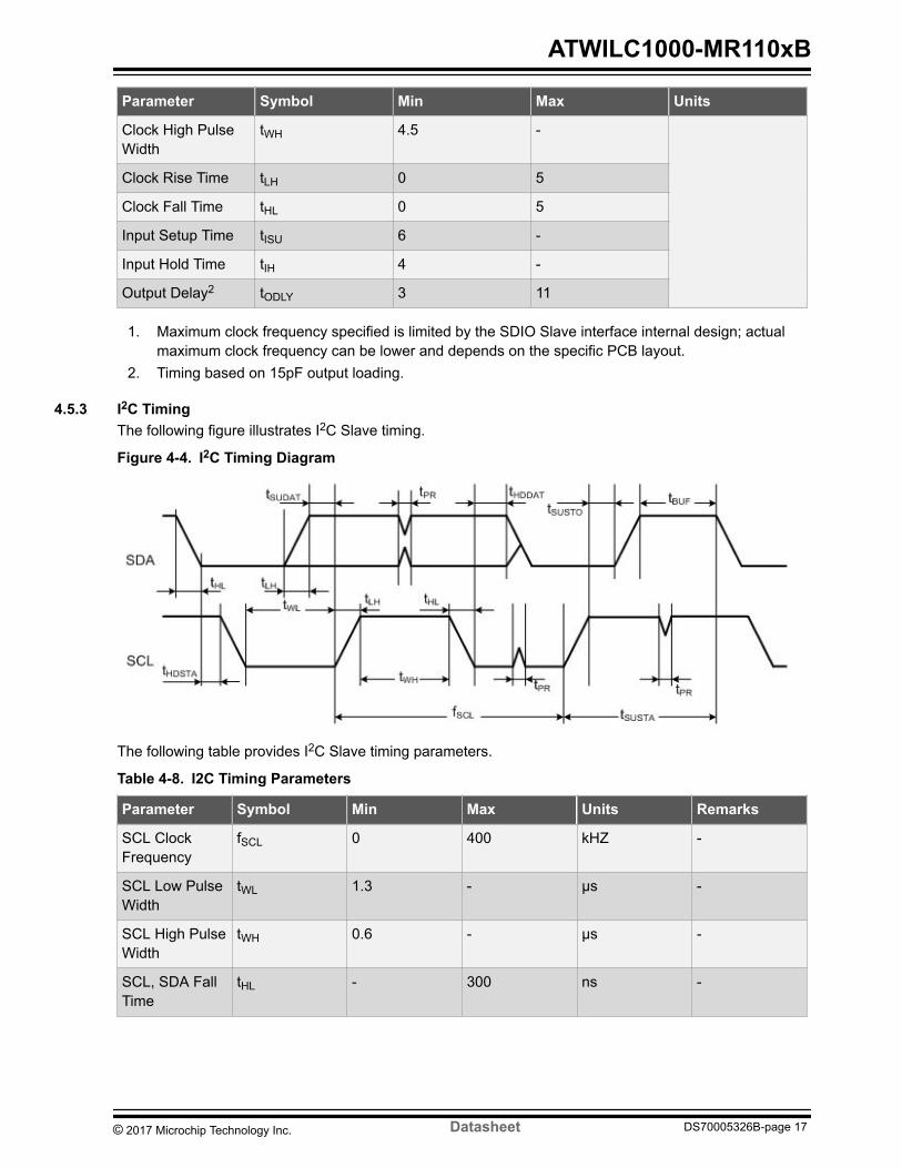
Parameter Symbol Min Max Units
Clock High PulseWidth
tWH 45 -
Clock Rise Time tLH 0 5
Clock Fall Time tHL 0 5
Input Setup Time tISU 6 -
Input Hold Time tIH 4 -
Output Delay2 tODLY 3 11
1 Maximum clock frequency specified is limited by the SDIO Slave interface internal design actualmaximum clock frequency can be lower and depends on the specific PCB layout
2 Timing based on 15pF output loading
453 I2C TimingThe following figure illustrates I2C Slave timing
Figure 4-4 I2C Timing Diagram
The following table provides I2C Slave timing parameters
Table 4-8 I2C Timing Parameters
Parameter Symbol Min Max Units Remarks
SCL ClockFrequency
fSCL 0 400 kHZ -
SCL Low PulseWidth
tWL 13 - micros -
SCL High PulseWidth
tWH 06 - micros -
SCL SDA FallTime
tHL - 300 ns -
ATWILC1000-MR110xB
copy 2017 Microchip Technology Inc Datasheet DS70005326B-page 17
Parameter Symbol Min Max Units Remarks
SCL SDA RiseTime
tLH - 300 ns This is dictatedby externalcomponents
START SetupTime
tSUSTA 06 - micros -
START HoldTime
tHDSTA 06 - micros -
SDA SetupTime
tSUDAT 100 - ns -
SDA Hold Time tHDDAT 0 - ns Slave andMaster Default
MasterProgrammingOption
40 - ns
STOP Setuptime
tSUSTO 06 - micros -
Bus Free TimeBetween STOPand START
tBUF 13 - micros -
Glitch PulseReject
tPR 0 50 ns -
ATWILC1000-MR110xB
copy 2017 Microchip Technology Inc Datasheet DS70005326B-page 18
5 Power ManagementThe ATWILC1000-MR110xB module has several device states
bull On statesndash ON_Transmit ndash device actively transmits an 80211 signal Highest output power and nominal
current consumptionndash ON_Receive ndash device actively receivies an 80211 signal Lowest sensitivity and nominal
current consumptionndash ON_Doze ndash device is powered on but it does not actively transmit or receive the datandash Power_Down ndash device core supply is powered off
The following pins are used to switch between the ON and Power_Down statesbull CHIP_EN ndash this pin (pin 22) enables or disables the DCDC converterbull VDDIO ndash IO supply voltage from external supply
In the ON states VDDIO is ON and CHIP_EN is high (at VDDIO voltage level) To change from the ONstates to Power_Down state connect the RESETN and CHIP_EN pin to logic low (GND) by following thepower down sequence mentioned in Power-UpDown Sequence When VDDIO is off and CHIP_EN islow the chip is powered off with no leakage (also see Restrictions for Power States)
51 Current Consumption in Various Device StatesThe following table provides this modules current consumption in various device states
Table 5-1 Current Consumption
Device State Code Rate Output
Power (dBm)
Current Consumption1
IVBATT IVDDIO
ON_Transmit 80211b 1Mbps 176 266 mA 22 mA
80211b 11Mbps 185 239 mA 22 mA
80211g 6Mbps 186 249 mA 22 mA
80211g 54Mbps 169 173 mA 22 mA
80211n MCS 0 177 253 mA 22 mA
80211n MCS 7 140 164 mA 22 mA
ON_Receive 80211b 1Mbps NA 63 mA 22 mA
80211b 11Mbps NA 63 mA 22 mA
80211g 6Mbps NA 63 mA 22 mA
80211g 54Mbps NA 63 mA 22 mA
80211n MCS 0 NA 63 mA 22 mA
80211n MCS 7 NA 63 mA 22 mA
ATWILC1000-MR110xB
copy 2017 Microchip Technology Inc Datasheet DS70005326B-page 19
Device State Code Rate Output
Power (dBm)
Current Consumption1
ON_Doze NA NA 380microA lt10microA
Power_Down NA NA 125 uA(2)
Note 1 The power consumption values are measured when VBAT is 33V and VDDIO is 33V at 25degC2 Current consumption mentioned for these states is the sum of current consumed in VDDIO and
VBAT voltage rails
52 Restrictions for Power StatesWhen no power is supplied to the device the DCDC Converter output and VDDIO are both turned off (atground potential) In this case a voltage cannot be applied to the device pins because each pin containsan ESD diode from the pin to supply This diode will turn on when voltage higher than one diode-drop issupplied to the pin
If a voltage must be applied to the signal pads while the chip is in a low power state the VDDIO supplymust be on so the Sleep mode or power-down state must be used
Similarly to prevent the pin-to-ground diode from turning on do not apply a voltage that is more than onediode-drop below ground to any pin
53 Power-UpDown SequenceThe following figure illustrates the power-updown sequence for the ATWILC1000-MR110xB module
Figure 5-1 Power-UpDown Sequence
The following table provides power-updown sequence timing parameters
ATWILC1000-MR110xB
copy 2017 Microchip Technology Inc Datasheet DS70005326B-page 20
Table 5-2 Power-UpDown Sequence Timing
Parameter Min Max Units Description Notes
tA 0 - ms VBAT rise toVDDIO rise
VBAT and VDDIO can risesimultaneously or connected togetherVDDIO must not rise before VBAT
tB 0 - ms VDDIO rise toCHIP_EN rise
CHIP_EN must not rise before VDDIOCHIP_EN must be driven high or lowand must not be left floating
tC 5 - ms CHIP_EN rise toRESETN rise
This delay is required to stabilize the XOclock before RESETN removal RESETNmust be driven high or low and must notbe left floating
tArsquo 0 - ms VDDIO fall toVBAT fall
VBAT and VDDIO fall simultaneously orconnected together VBAT must not fallbefore VDDIO
tBrsquo 0 - ms CHIP_EN fall toVDDIO fall
VDDIO must not fall before CHIP_ENCHIP_EN and RESETN must fallsimultaneously
tCrsquo 0 - ms RESETN fall toVDDIO fall
VDDIO must not fall before RESETNRESETN and CHIP_EN fallsimultaneously
54 Digital IO Pin Behavior During Power-Up SequencesThe following table represents the digital IO pin states corresponding to the device power modes
Table 5-3 Digital IO Pin Behavior in Different Device States
Device State VDDIO CHIP_EN RESETN Output Driver InputDriver
Pull UpDownResistor (96
kOhm)
Power_Down coresupply OFF
High Low Low Disabled (Hi-Z) Disabled Disabled
Power-On Resetcore supply and hardreset ON
High High Low Disabled (Hi-Z) Disabled Enabled
Power-On Defaultcore supply ONdevice out of resetand not programmed
High High High Disabled (Hi-Z) Enabled Enabled
On_Doze
On_Transmit
High High High Programmedby firmware foreach pinenabled ordisabled
Oppositeof OutputDriverstate
Programmedby firmware foreach pinenabled ordisabled
ATWILC1000-MR110xB
copy 2017 Microchip Technology Inc Datasheet DS70005326B-page 21
Device State VDDIO CHIP_EN RESETN Output Driver InputDriver
Pull UpDownResistor (96
kOhm)
On_Receive coresupply ON deviceprogrammed byfirmware
ATWILC1000-MR110xB
copy 2017 Microchip Technology Inc Datasheet DS70005326B-page 22
6 CPU and Memory Subsystems
61 ProcessorThis ATWILC1000-MR110xB module has a Cortus APS3 32-bit processor This processor performs manyof the MAC functions including but not limited to association authentication power management securitykey management and MSDU aggregationdeaggregation In addition the processor provides flexibility forvarious modes of operation such as STA and AP modes
62 Memory SubsystemThe APS3 core uses a 128 KB instructionboot ROM along with a 160 KB instruction RAM and a 64 KBdata RAM In addition the device uses a 128 KB shared RAM accessible by the processor and MAC thatallows the APS3 core to perform various data management tasks on the Tx and Rx data packets
63 Nonvolatile Memory (eFuse)This ATWILC1000-MR110xB module has 768 bits of nonvolatile eFuse memory that is read by the CPUafter device reset This nonvolatile One-Time-Programmable (OTP) memory is used to store customerspecific parameters such as MAC address various calibration information such as Tx power crystalfrequency offset etc and other software-specific configuration parameters The eFuse is partitioned intosix 128 bit banks Each bank has the same bit map mentioned in the following figure The purpose of thefirst 80 bits in each bank is fixed and the remaining 48 bits are general purpose software dependent bitsEach bank is programmed independently which allows for several updates of the device parametersfollowing the initial programming For example if the MAC address has to be changed Bank 1 has to beprogrammed with the new MAC address along with the values of TX gain correction and Frequency offsetif they are used and programmed in the Bank 0 The contents of Bank 0 have to be invalidated in thiscase by programming the Invalid bit in the Bank 0 This will allow the firmware to use the MAC addressfrom Bank 1
By default all the ATWILC1000-MR110PB and ATWILC1000-MR110UB modules are programmed withthe MAC address and the Frequency offset bits of Bank 0
ATWILC1000-MR110xB
copy 2017 Microchip Technology Inc Datasheet DS70005326B-page 23
Figure 6-1 eFuse Bit Map
ATWILC1000-MR110xB
copy 2017 Microchip Technology Inc Datasheet DS70005326B-page 24
7 WLAN SubsystemThe WLAN subsystem is composed of the Media Access Controller (MAC) Physical Layer (PHY) andthe radio
71 MAC
711 DescriptionThis module is designed to operate at low power while providing high data throughput The IEEE 80211MAC functions are implemented with a combination of dedicated datapath engines hardwired controllogic and a low power high-efficiency microprocessor The combination of dedicated logic with aprogrammable processor provides optimal power efficiency and real time response while providing theflexibility to accommodate evolving standards and future feature enhancements
The dedicated datapath engines are used to implement data path functions with heavy computationalrequirements For example a Frame Check Sequence (FCS) engine checks the Cyclic RedundancyCheck (CRC) of the transmitting and receiving packets and a cipher engine performs all the requiredencryption and decryption operations for the WEP WPA-TKIP WPA2 CCMP-AES and WPA2 Enterprisesecurity requirements
Control functions which have real time requirements are implemented using hardwired control logicmodules These logic modules offer real time response while maintaining configurability through theprocessor Examples of hardwired control logic modules are the channel access control module(implements EDCAHCCA Beacon Tx control interframe spacing and so on) protocol timer module(responsible for the Network Access vector back-off timing timing synchronization function and slotmanagement) MAC Protocol Data Unit (MPDU) handling module aggregationdeaggregation moduleblock ACK controller (implements the protocol requirements for burst block communication) and TxRxcontrol Finite State Machine (FSM) (coordinate data movement between PHY and MAC interface cipherengine and the Direct Memory Acces (DMA) interface to the TxRx FIFOs)
Following are the characteristics of MAC functions implemented solely in software on the microprocessor
bull Functions with high memory requirements or complex data structures Examples are associationtable management and power save queuing
bull Functions with low computational load or without critical real time requirements Examples areauthentication and association
bull Functions that require flexibility and upgradeability Examples are beacon frame processing andQoS scheduling
712 FeaturesThe ATWILC1000-MR110xB IEEE 80211 MAC supports the following functions
bull IEEE 80211bgnbull IEEE 80211e WMM QoS EDCAPCF multiple access categories traffic schedulingbull Advanced IEEE 80211n features
ndash Transmission and reception of aggregated MPDUs (A-MPDU)ndash Transmission and reception of aggregated MSDUs (A-MSDU)ndash Immediate block acknowledgmentndash Reduced Interframe Spacing (RIFS)
bull Supports IEEE 80211i and WFA security with key management
ATWILC1000-MR110xB
copy 2017 Microchip Technology Inc Datasheet DS70005326B-page 25
ndash WEP 64128ndash WPA-TKIPndash 128-bit WPA2 CCMP (AES)ndash WPA2 Enterprise
bull Advanced power managementndash Standard IEEE 80211 Power save modendash Wi-Fi alliance WMM-PS (U-APSD)
bull RTS-CTS and CTS self supportbull Supports either STA or AP mode in the infrastructure basic service set modebull Supports concurrent mode of operationbull Supports Independent Basic Service Set (IBSS)
72 PHYThe ATWILC1000-MR110xB module WLAN PHY is designed to achieve reliable and power-efficientphysical layer communication specified by IEEE 80211 bgn in single stream mode with 20 MHzbandwidth The advanced algorithms are used to achieve maximum throughput in a real worldcommunication environment with impairments and interference The PHY implements all the requiredfunctions such as Fast Fourier Transform (FFT) filtering Forward Error Correction (FEC) that is a Viterbidecoder frequency timing acquisition and tracking channel estimation and equalization carrier sensingclear channel assessment and automatic gain control
Features
The IEEE 80211 PHY supports the following functions
bull Single antenna 1x1 stream in 20 MHz channelsbull Supports IEEE 80211b DSSS-CCK modulation 1 2 55 and 11 Mbpsbull Supports IEEE 80211g OFDM modulation 6 9 1218 24 36 48 and 54 Mbpsbull Supports IEEE 80211n HT modulations MCS0-7 20 MHz 800 and 400ns guard interval 65 72
130 144 195 217 260 289 390 433 520 578 585 650 and 722 Mbpsbull IEEE 80211n mixed mode operationbull Per packet Tx power controlbull Advanced channel estimationequalization automatic gain control CCA carriersymbol recovery
and frame detection
721 FeaturesThe IEEE 80211 PHY supports the following functions
bull Single antenna 1x1 stream in 20 MHz channelsbull Supports IEEE 80211b DSSS-CCK modulation 1 2 55 and 11 Mbpsbull Supports IEEE 80211g OFDM modulation 6 9 1218 24 36 48 and 54 Mbpsbull Supports IEEE 80211n HT modulations MCS0-7 20 MHz 800 and 400ns guard interval 65 72
130 144 195 217 260 289 390 433 520 578 585 650 and 722 Mbpsbull IEEE 80211n mixed mode operationbull Per packet Tx power controlbull Advanced channel estimationequalization automatic gain control CCA carriersymbol recovery
and frame detection
ATWILC1000-MR110xB
copy 2017 Microchip Technology Inc Datasheet DS70005326B-page 26
73 RadioThis section describes the properties and characteristics of the ATWILC1000- MR110xB and Wi-Fi radiotransmit and receive performance capabilities of the device The performance measurements are taken atthe RF pin assuming 50Ω impedance the RF performance is guaranteed for room temperature of 25degCwith a derating of 2-3dB at boundary conditions
Measurements were taken under typical conditions VBATT at 33V VDDIO at 33V and temperature at+25ordmC
Table 7-1 Features and Properties
Feature Description
Module Part Number ATWILC1000-MR110xB
WLAN Standard IEEE 80211bgn Wi-Fi compliant
Host Interface SPI SDIO
Dimension L x W x H 217 x 147 x 21 (typical) mm
Frequency range 2412 GHz ~ 2472 GHz (24 GHz ISM band)
Number of channels 11 for North America 13 for Europe
Modulation 80211b DQPSK DBPSK CCK
80211gn OFDM64-QAM16-QAM QPSK BPSK
Data rate 80211b 1 2 55 11 Mbps80211g 6 9 12 18 24 36 48 54 Mbps
Data rate
(20 MHz short GI400ns)
80211n 72 144 217 289 433 578 65722Mbps
Operating temperature(1) -40degC to 85degC
Storage temperature -40degC to 125degC
Humidity Operating humidity 10 to 95 non-condensing
Storage humidity 5 to 95 non-condensing
Note 1 RF performance is guaranteed at room temperature of 25degC with a 2-3db change at boundary
conditions
ATWILC1000-MR110xB
copy 2017 Microchip Technology Inc Datasheet DS70005326B-page 27
8 External InterfacesThis section describes the various host and debug interfaces of the ATWILC1000-MR110xB module
81 Interfacing with the Host MicrocontrollerThis section describes how to interface ATWILC1000-MR110xB module with the host microcontroller Theinterface comprises of a slave SPISDIO and additional control signals as shown in the figure Additionalcontrol signals are connected to the GPIOIRQ interface of the microcontroller
Figure 8-1 Interfacing with the Host Microcontroller
Table 8-1 Host Microcontroller Interface Pins
Module Pin Function(1)
4 RESET_N
11 WAKE
13 IRQ_N
22 CHIP_EN
16 SPI_SSNSD_DATA1
15 SPI_MOSISD_DATA2
17 SPI_MISOSD_DATA0
18 SPI_SCKSD_CMD
ATWILC1000-MR110xB
copy 2017 Microchip Technology Inc Datasheet DS70005326B-page 28
Module Pin Function(1)
14 SD_DATA3
19 SD_CLK
Note 1 Logic input for module pin SDIO_SPI_CFG(10) determines whether SDIO or SPI slave interface is
enabled Connect SDIO_SPI_CFG to VDDIO through a 1MΩ resistor to enable the SPI interfaceConnect SDIO_SPI_CFG to ground to enable SDIO interface
2 It is recommended to place test points for pins I2C_SDA(3) I2C_SCL(2) GPIO_3(25) andGPIO_5(27) in the design
82 SPI Slave InterfaceThe SPI slave interface can be enabled by connecting the SDIO_SPI_CFG pin to VDDIO This SPIinterface is used to exchange the control and 80211 data The SPI is a full duplex slave-synchronousserial interface that is available following reset when pin 10 (SDIO_SPI_CFG) is connected to VDDIO
The SPI interface pin mapping configuration is provided in the following table
Table 8-2 SPI Interface Pin Mapping
Pin SPI Function
10 SDIO_SPI_CFG Must be connected to VDDIO
16 SSN Active-Low Slave Select
15 MOSI Serial Data Receive
18 SCK Serial Clock
17 MISO Serial Data Transmit
When the SPI is not selected ie when SSN is high the SPI interface will not interfere with datatransfers between the serial master and other serial slave devices When the serial slave is not selectedits transmitted data output is buffered resulting in a high impedance drive onto the MISO line
The SPI interface responds to a protocol that allows an external host to read or write any register in thechip and also initiate DMA transfers
The SPI SSN MOSI MISO and SCK pins of this module have internal programmable pull up resistorsThese resistors are programmed to be disabled Otherwise if any of the SPI pins are driven to a low levelwhile this module is in the low power sleep state current will flow from the VDDIO supply through the pullup resistors increasing the current consumption of the module
83 SDIO Slave InterfaceThe SDIO interface is enabled by connecting the SDIO_SPI_CFG pin to ground This SDIO interface isused to exchange the control and 80211 data The SDIO interface is available after reset when pin 10(SDIO_SPI_CFG) is connected to ground
This SDIO is a full speed interface The interface supports the 1-bit4-bit SD transfer mode at the clockrange of 0-50 MHz The host uses this interface to read and write from any register within the chip andalso configures this module for DMA data transfer
ATWILC1000-MR110xB
copy 2017 Microchip Technology Inc Datasheet DS70005326B-page 29
The SDIO interface pin mapping configuration is provided in the following table
Table 8-3 ATWILC1000 SDIO Interface Pin Mapping
Pin SDIO Function
10 SDIO_SPI_CFG Must be connected to ground
14 DAT3 Data 3
15 DAT2 Data 2
16 DAT1 Data 1
17 DAT0 Data 0
18 CMD Command
19 CLK Clock
The SDIO card is detected when the it is inserted into an SDIO host During the normal initialization andinterrogation of the card by the host the card identifies itself as an SDIO device The host softwareobtains the card information in a tuple (linked list) format and determines if that cardrsquos IO function(s) areacceptable to activate If the card is acceptable it is allowed to power-up fully and start the IO function(s)built into the card
The SD memory card communication is based on an advanced 9-pin interface (clock command fourdata and three power lines) designed to operate at maximum operating frequency of 50 MHz
831 Featuresbull Compliant with SDIO card specification version 20bull Host clock rate variable between 0 and 50 MHzbull Supports 1-bit4-bit SD bus modesbull Allows card to interrupt hostbull Responds to direct readwrite (IO52) and extended readwrite (IO53) transactionsbull Supports suspendresume operation
84 UART Debug InterfaceThis module has a Universal Asynchronous ReceiverTransmitter (UART) interface on J25(RxD) andJ27(TxD) pins This interface should be used only for debugging purposes The UART is compatible withthe RS-232 standard where ATWILC1000-MR110xB operates as Data Terminal Equipment (DTE) It hasa two-pin RXDTXD interface
The default configuration for accessing the UART interface of ATWILC1000-MR110xB is mentionedbelow
bull Baud rate 115200bull Data 8 bitbull Parity Nonebull Stop bit 1 bitbull Flow control None
It also has Rx and Tx FIFOs which ensures reliable high speed reception and low software overheadtransmission FIFO size is 4x8 for both Rx and Tx direction The UART has status registers that show the
ATWILC1000-MR110xB
copy 2017 Microchip Technology Inc Datasheet DS70005326B-page 30
number of received characters available in the FIFO and various error conditions in addition it has theability to generate interrupts based on these status bits
An example of UART receiving or transmitting a single packet is shown in the following figure Thisexample shows 7-bit data (0x45) odd parity and two stop bits
Figure 8-2 Example of UART RX or TX Packet
85 I2C Slave InterfaceThis module provides an I2C bus slave that allows for easy debugging of the ATWILC1000-MR110xBdevices It supports I2C bus Version 21 ndash 2000
The I2C interface is used only for debug This interface is a two-wire serial interface consisting of a serialdata line (SDA Pin 17) and a serial clock (SCL Pin 18) It responds to seven bit address value 0x60This module I2C interface operates in standard mode (with data rates up to 100Kbs) and fast mode (withdata rates up to 400Kbs)
The I2C is a synchronous serial interface The SDA line is a bidirectional signal and changes only whenthe SCL line is low except for STOP START and RESTART conditions The output drivers are open-drain to perform wire AND functions on the bus The devices on the bus are limited to the 400pFcapacitance Data is transmitted in byte packages
For specific information refer to the Philips Specification entitled ldquoThe I2C -Bus Specification Version21rdquo
ATWILC1000-MR110xB
copy 2017 Microchip Technology Inc Datasheet DS70005326B-page 31
9 Notes on Interfacing with the ATWILC1000-MR110xBProgrammable Pull up Resistors
The ATWILC1000-MR110xB module provides programmable pull up resistors on various pins Thepurpose of these resistors is to keep any unused input pins from floating which causes excess current toflow through the input buffer from the VDDIO supply Any unused pin on the device must leave these pullup resistors enabled so that the pin will not float The default state at power-up is for the pull up resistorto be enabled however any pin that is used must have the pull up resistor disabled The reason for thisis that if any pins are driven to a low level while the device is in the low power sleep state current flowsfrom the VDDIO supply through the pull up resistors increasing the current consumption of the moduleSince the value of the pull up resistor is approximately 100 kOhm the current through any pull up resistorthat is being driven low is VDDIO100K For VDDIO = 33V the current is approximately 33 microA The pinsthat are used and have programmable the pull up resistor disabled should always be actively driven toeither a high or low level and not be allowed to float
ATWILC1000-MR110xB
copy 2017 Microchip Technology Inc Datasheet DS70005326B-page 32
10 Application Reference DesignThis section provides reference schematic for ATWILC1000-MR110xB module with SPI and SDIO hostinterfacesFigure 10-1 ATWILC1000-MR110xB Reference Schetmatic - SDIO Host Interface
Table 10-1 ATWILC1000-MR110xB reference Schematic - SDIO Host Interface - Bill of Materials
Item Qty Reference Value Description
Manufacturer
PartNumber
Footprint
1 9 R2 R3R4R5 R6R7 R8R9 R10
0 R RESISTORThick Film0 ohm0402
Yageo RC0402JR-070RL
0402
2 1 U1 ATWILC1000-MR110xB
Wi-FiModule
Microchip ATWILC1000-MR110xB
ATWILC1000-MR110xB
copy 2017 Microchip Technology Inc Datasheet DS70005326B-page 33
Figure 10-2 ATWILC1000-MR110xB Reference Schetmatic - SPI Host Interface
Table 10-2 ATWILC1000-MR110xB reference Schematic - SPI Host Interface - Bill of Materials
Item Qty Reference Value Description
Manufacturer
PartNumber
Footprint
1 1 R1 1 M RESISTORThick Film1 M ohm0402
Yageo RC0100FR-071ML
0402
2 9 R2 R3R4R5 R6R7 R8R9 R10
0 R RESISTORThick Film0 ohm0402
Yageo RC0402JR-070RL
0402
3 1 U1 ATWILC1000-MR110xB
Wi-FiModule
Microchip ATWILC1000-MR110xB
ATWILC1000-MR110xB
copy 2017 Microchip Technology Inc Datasheet DS70005326B-page 34
11 Module Outline DrawingsThe ATWILC1000-MR110PB module package details are outlined in the following figure Dimensions arein mm
Figure 11-1 Module Drawings ndash ATWILC1000-MR110PB - Top Bottom and Side Views
MODULE TOP VIEW
Metal Shield
Metal Shield
PCB
MODULE SIDE VIEW MODULE BOTTOM VIEW
NOTE THIS PAD MUST BE SOLDERED TO GND
NOT TO SCALE
The ATWILC1000-MR110UB module package details are outlined in the following figure Dimensions arein mm
ATWILC1000-MR110xB
copy 2017 Microchip Technology Inc Datasheet DS70005326B-page 35
Figure 11-2 Module Drawings ndash ATWILC1000-MR110UB - Top Bottom and Side Views
MODULE TOP VIEW
Metal Shield
Metal Shield
PCB
MODULE SIDE VIEW MODULE BOTTOM VIEW
NOTE THIS PAD MUST BE SOLDERED TO GND
NOT TO SCALE Rev 2
This section provides the outline drawing for the recommended footprint for the ATWILC1000-MR110xBmodule It is imperative that the center Ground Pad is provided with an array of GND vias to provide agood ground and act as thermal sink for the ATWILC1000-MR110xB module
ATWILC1000-MR110xB
copy 2017 Microchip Technology Inc Datasheet DS70005326B-page 36
Figure 11-3 Recommended Solder Pad Footprint
NOTE THIS PAD MUST BE TIED TO GND
1016 Pitch
1473
19
08
1016 Pitch
4064
267
267
600
1016 Pitch
370
370
1016 Pitch
19 3048
368
2172 2032
442
SOLDER PAD FOOTPRINT
Drawing not to scaleUntoleranced dimensionsUnits=mm
ATWILC1000-MR110xB
copy 2017 Microchip Technology Inc Datasheet DS70005326B-page 37
12 Design ConsiderationThis section provides the guidelines on placement and routing to achieve the best performance
121 ATWILC1000-MR110PB Placement and Routing GuidelinesIt is critical to follow the recommendations listed below to achieve the best RF performance
bull The module must be placed on host board The printed antenna area must overlap with the carrierboard The portion of the module containing the antenna should not stick out over the edge of thehost board The antenna is designed to work properly when it is sitting directly on top of a 15mmthick printed circuit board Figure 12-2 shows the best poor and worst case module placements inhost board
bull If the module is placed at the edge of the host board a minimum 22mm by 5 mm area directlyunder the antenna must be clear of all metal on all layers of the board ldquoIn-landrdquo placement isacceptable however deepness of keep-out area must grove to module edge to host board edgeplus 5 mmNote Do not place the module in the middle of the host board or far away from the host boardedge
bull Follow the module placement keepout host PCB cutout recommendation as shown in Figure 12-1ndash Avoid routing any traces in the highlighted region on the top layer of the host board which will
be directly below the module areandash Follow the electrical keepout layer recommendation as shown in Figure 12-1 There should be
no copper in all layers of the host board in this region Avoid placing any components (likemechanical spacers bumpon etc) in the recommended electrical keepout area
ndash Place GND polygon pour below the module with the recommended boundary in the top layerof the host board as shown in Figure 12-1 Do not have any breaks in this GND plane
ndash Place sufficient GND vias in the highlighted area below the module for better RFperformance
ndash It is recommended to have a 3x3 grid of GND vias solidly connecting the exposed GNDpaddle of the module to the inner layer ground plane This will act as a good ground andthermal conduction for the ATWILC1000-MR110PB module The GND vias should have aminimum via hole size of 03mm
ndash Follow the mechanical boundary of the host PCB as shown in the Figure 12-1bull Keep the large metal objects away from antenna to avoid electromagnetic field blockingbull Do not enclose the antenna within a metal shieldbull Keep any components which may radiate noise or signals within the 24 GHz ndash 25 GHz frequency
band away from the antenna and if possible shield those components Any noise radiated from thehost board in this frequency band will degrade the sensitivity of the module
bull Make sure the width of the traces routed to GND VDDIO and VBAT rails are sufficiently larger forhandling the peak Tx current consumption
ATWILC1000-MR110xB
copy 2017 Microchip Technology Inc Datasheet DS70005326B-page 38
Figure 12-1 ATWILC1000-MR110PB Placement Reference
Figure 12-2 ATWILC1000-MR110PB Placement Example
122 Printed PCB Antenna Performance of ATWILC1000-MR110PBThe printed PCB antenna on the ATWILC1000-MR110PB is a meandered Inverted F Antenna (IFA) Theantenna is fed via matching network which is matched for the module installed on 15mm thick mainboard Main board thickness deviation by plusmn1mm changes RXTX performance by plusmn1dB maximumreferring to RXTX performance with default antenna matching network and installed on 15mm thick mainboard
Measured antenna gain is -03dBi
ATWILC1000-MR110xB
copy 2017 Microchip Technology Inc Datasheet DS70005326B-page 39
Antenna Radiation PatternFollowing figures illustrate the antenna radiation pattern During the measurement the printed antenna isplaced in the XZ plane with Y axis being perpendicular to the module and pointing to the back of themoduleFigure 12-3 Antenna Radiation Pattern when Phi = 0 degree
Figure 12-4 Antenna Radiation Pattern when Phi = 90 degree
ATWILC1000-MR110xB
copy 2017 Microchip Technology Inc Datasheet DS70005326B-page 40
Figure 12-5 Antenna Radiation Pattern when Theta = 90 degree
ATWILC1000-MR110xB
copy 2017 Microchip Technology Inc Datasheet DS70005326B-page 41
123 ATWILC1000-MR110UB Placement and Routing GuidelinesThe ATWILC1000-MR110UB module has an Ultra Small Miniature RF Connector (uFL) for the externalantenna
The choice of antenna is limited to the antenna types for which the module was tested and approved Fora list of tested and approved antennas that may be used with the module refer to the respective countryin the Regulatory Approval section
An approved and tested antenna type is shown in the following Table
Table 12-1 Tested External Antenna Type
Antenna Type Gain
PCB Antenna 20 dBi
ATWILC1000-MR110xB
copy 2017 Microchip Technology Inc Datasheet DS70005326B-page 42
1231 Recommended External Antenna for ATWILC1000-MR110UBPCB Antenna (Part number W3525B039) along with a 10cm length RF cable assembly (uFL to SMA)has been used for the certification of ATWILC1000-MR110UB It is recommended to use the same orsimilar external antenna in design
ATWILC1000-MR110xB
copy 2017 Microchip Technology Inc Datasheet DS70005326B-page 43
13 Reflow Profile InformationThis section provides the guidelines for the reflow process to get the module soldered to the customersdesign
131 Storage Condition
1311 Moisture Barrier Bag Before OpeningA moisture barrier bag must be stored in a temperature of less than 30degC with humidity under 85 RHThe calculated shelf life for the dry-packed product shall be 12 months from the date the bag is sealed
1312 Moisture Barrier Bag OpenHumidity indicator cards must be blue indicating that the humidity is lt30
132 Solder PasteSnAgCu eutectic solder with melting temperature of 217degC is most commonly used for lead-free solderreflow application This alloy is widely accepted in the semiconductor industry due to its low costrelatively low melting temperature and good thermal fatigue resistance Some recommended pastesinclude NC-SMQreg 230 flux and Indalloyreg 241 solder paste made up of 955 Sn38 Ag07 Cu or SENJUN705-GRN3360-K2-V Type 3 no clean paste
133 Stencil DesignThe recommended stencil is laser-cut stainless-steel type with thickness of 100 microm to 130 microm andapproximately a 11 ratio of stencil opening to pad dimension To improve paste release a positive taperwith bottom opening 25 microm larger than the top is utilized Local manufacturing experience may find othercombinations of stencil thickness and aperture size to get good results
134 Printing ProcessThe printing process requires no significant changes compared to SnPb solder Any guidelinesrecommended by the paste manufacturers to accommodate paste specific characteristics should befollowed Post-print inspection and paste volume measurement is very critical to ensure good print qualityand uniform paste
135 Baking ConditionsThis module is rated at MSL level 3 After the sealed bag is opened no baking is required within 168hours as long as the devices are held at le 30degC60 RH or stored at lt 10 RH
The module requires baking before mounting ifbull The sealed bag has been open for more than 168 hoursbull The humidity indicator card reads more than 10bull SIPs need to be baked for eight hours at 125degC
ATWILC1000-MR110xB
copy 2017 Microchip Technology Inc Datasheet DS70005326B-page 44
136 Soldering and Reflow ConditionOptimization of the reflow process is the most critical factor considered for lead-free soldering Thedevelopment of an optimal profile must account the paste characteristics the size of the board thedensity of the components the mix of the larger and smaller components and the peak temperaturerequirements of the components An optimized reflow process is the key to ensuring a successful lead-free assembly and achieves high yield and long-term solder joint reliability
Temperature ProfilingTemperature profiling must be performed for all new board designs by attaching thermocouples at thesolder joints on the top surface of the larger components and at multiple locations of the boards This isto ensure that all components are heated to a temperature above the minimum reflow temperatures andthe smaller components do not exceed the maximum temperature limit The SnAgCu solder alloy melts at~217degC so the reflow temperature peak at joint level must be 15 to 20degC higher than meltingtemperature The targeted solder joint temperature for the SnAgCu solder must be ~235degC For larger orsophisticated boards with a large mix of components it is also important to ensure that the temperaturedifference across the board is less than 10 degrees to minimize board warpage The maximumtemperature at the component body must not exceed the MSL3 qualification specification
1361 Reflow OvenIt is strongly recommended that a reflow oven equipped with more heating zones and Nitrogenatmosphere be used for lead-free assembly Nitrogen atmosphere has shown to improve the wet-abilityand reduce temperature gradient across the board It can also enhance the appearance of the solderjoints by reducing the effects of oxidation
The following items should also be observed in the reflow process1 Some recommended pastes include
ndash NC-SMQreg 230 flux and Indalloyreg 241 solder paste made up of 955 Sn38 Ag07 Cundash SENJU N705-GRN3360-K2-V Type 3 no clean paste
2 Allowable reflow soldering iterationsndash Three times based on the following reflow soldering profile (refer following Figure)
3 Temperature profilendash Reflow soldering shall be done according to the following temperature profile (refer to the
following figure)ndash Peak temperature 250degC
ATWILC1000-MR110xB
copy 2017 Microchip Technology Inc Datasheet DS70005326B-page 45
Figure 13-1 Solder Reflow Profile
Cleaning
The exposed ground paddle helps to self-align the module avoiding pad misalignment The use of no-clean solder pastes is recommended Full drying of no-clean paste fluxes must be ensured as a result ofthe reflow process This may require longer reflow profiles andor peak temperatures toward the high endof the process window as recommended by the solder paste vendor It is believed that uncured fluxresidues could lead to corrosion andor shorting in accelerated testing and possibly the field
Rework
Rework is to remove the mounted SIP package and replace with a new unit It is recommended that oncean ATWILC1000-MR110xB module has been removed it should never be reused During the reworkprocess the mounted module and PCB are heated partially and the module is removed It isrecommended to heat-proof the proximity of the mounted parts and junctions and use the best nozzle forrework that is suited to the module size
ATWILC1000-MR110xB
copy 2017 Microchip Technology Inc Datasheet DS70005326B-page 46
14 Module Assembly ConsiderationsThe ATWILC1000-MR110xB modules are assembled with an EMI Shield to ensure compliance with EMIemission and immunity rules The EMI shield is made of a tin-plated steel (SPTE) and is not hermeticallysealed Solutions like IPA and similar solvents can be used to clean the ATWILC1000-MR110xB modulehowever cleaning solutions that contain acid should never be used on the module
The ATWILC1000-MR110xB modules are manufactured without any conformal coating applied It is thecustomerrsquos responsibility if a conformal coating is specified and applied to the ATWILC1000- MR110xBmodule
ATWILC1000-MR110xB
copy 2017 Microchip Technology Inc Datasheet DS70005326B-page 47
15 Regulatory ApprovalRegulatory approvals received
ATWILC1000-MR110PBbull United StatesFCC ID 2ADHKATWILC1000bull CanadaISED
ndash IC 20266-ATWILC1000ndash HVIN ATWILC1000-MR110PB
bull Europe - CE
ATWILC1000-MR110UBbull United StatesFCC ID 2ADHKATWILC1000U
151 United StatesThe ATWILC1000-MR110PB and ATWILC1000-MR110UB modules have received FederalCommunications Commission (FCC) CFR47 Telecommunications Part 15 Subpart C ldquoIntentionalRadiatorsrdquo single-modular approval in accordance with Part 15212 Modular Transmitter approval Single-modular transmitter approval is defined as a complete RF transmission sub-assembly designed to beincorporated into another device that must demonstrate compliance with FCC rules and policiesindependent of any host A transmitter with a modular grant can be installed in different end-use products(referred to as a host host product or host device) by the grantee or other equipment manufacturer thenthe host product may not require additional testing or equipment authorization for the transmitter functionprovided by that specific module or limited module device
The user must comply with all of the instructions provided by the Grantee which indicate installationandor operating conditions necessary for compliance
A host product itself is required to comply with all other applicable FCC equipment authorizationregulations requirements and equipment functions that are not associated with the transmitter moduleportion For example compliance must be demonstrated to regulations for other transmitter componentswithin a host product to requirements for unintentional radiators (Part 15 Subpart B) such as digitaldevices computer peripherals radio receivers etc and to additional authorization requirements for thenon-transmitter functions on the transmitter module (ie Verification or Declaration of Conformity) asappropriate (eg Bluetooth and Wi-Fi transmitter modules may also contain digital logic functions)
1511 Labeling and User Information RequirementsThe ATWILC1000-MR110PB and ATWILC1000-MR110UB modules have been labeled with their ownFCC ID numbers If the FCC ID is not visible when the module is installed inside another device then theoutside of the finished product into which the module is installed must display a label referring to theenclosed module This exterior label can use wording as follows
For the ATWILC1000-MR110PB
Contains Transmitter Module FCC ID 2ADHKATWILC1000 or
Contains FCC ID 2ADHKATWILC1000
This device complies with Part 15 of the FCC Rules Operation is subject to the following twoconditions (1) this device may not cause harmful interference and (2) this device must acceptany interference received including interference that may cause undesired operation
ATWILC1000-MR110xB
copy 2017 Microchip Technology Inc Datasheet DS70005326B-page 48
For the ATWILC1000-MR110UB
Contains Transmitter Module FCC ID 2ADHKATWILC1000U or
Contains FCC ID 2ADHKATWILC1000U
This device complies with Part 15 of the FCC Rules Operation is subject to the following twoconditions (1) this device may not cause harmful interference and (2) this device must acceptany interference received including interference that may cause undesired operation
A users manual for the finished product should include the following statement
This equipment has been tested and found to comply with the limits for a Class B digital devicepursuant to part 15 of the FCC Rules These limits are designed to provide reasonable protectionagainst harmful interference in a residential installation This equipment generates uses and can radiateradio frequency energy and if not installed and used in accordance with the instructions may causeharmful interference to radio communications However there is no guarantee interference will not occurin a particular installation If this equipment does cause harmful interference to radio or televisionreception which can be determined by turning the equipment off and on the user is encouraged to tryto correct the interference by one or more of the following measures
bull Reorient or relocate the receiving antennabull Increase the separation between the equipment and receiverbull Connect the equipment into an outlet on a circuit different from that to which the receiver is
connectedbull Consult the dealer or an experienced radioTV technician for help
Additional information on labeling and user information requirements for Part 15 devices can be found inKDB Publication 784748 which is available at the FCC Office of Engineering and Technology (OET)Laboratory Division Knowledge Database (KDB) httpsappsfccgovoetcfkdbindexcfm
1512 RF ExposureAll transmitters regulated by FCC must comply with RF exposure requirements KDB 447498 General RFExposure Guidance provides guidance in determining whether proposed or existing transmitting facilitiesoperations or devices comply with limits for human exposure to Radio Frequency (RF) fields adopted bythe Federal Communications Commission (FCC)
From the FCC Grant Output power listed is conducted This transmitter is restricted for use with thespecific antenna(s) tested in this application for Certification
In the end product the antenna(s) used with this transmitter must be installed to provide a separationdistance of at least 65 cm from all persons and must not be co-located or operation in conjunction withany other antenna or transmitter User and installers must be provided with antenna installationinstructions and transmitter operating conditions for satisfying the RF exposure compliance
1513 Approved Antenna TypesTo maintain modular approval in the United States only the antenna types that have been tested shall beused It is permissible to use a different antenna provided the same antenna type and antenna gain(equal to or less than) is used An antenna type comprises antennas having similar in-band and out-of-band radiation patterns
Testing the ATWILC1000-MR110UB module was performed with the antenna types listed in Table 12-1
ATWILC1000-MR110xB
copy 2017 Microchip Technology Inc Datasheet DS70005326B-page 49
1514 Helpful WebsitesFederal Communications Commission (FCC) httpwwwfccgov
FCC Office of Engineering and Technology (OET) Laboratory Division Knowledge Database (KDB) httpsappsfccgovoetcfkdbindexcfm
152 CanadaThe ATWILC1000-MR110PB module has been certified for use in Canada under Innova- tion Scienceand Economic Development Canada (ISED formerly Industry Canada) Radio Standards Procedure(RSP) RSP-100 Radio Standards Specifi- cation (RSS) RSS-Gen and RSS-247 Modular approvalpermits the installation of a module in a host device without the need to recertify the device
1521 Labeling and User Information RequirementsLabel Requirements (from RSP-100 Issue 11 Section 3) The host device shall be properly labeled toidentify the module within the host device
The Innovation Science and Economic Development Canada certification label of a module shall beclearly visible at all times when installed in the host device otherwise the host device must be labeled todisplay the Innovation Science and Economic Development Canada certification number of the modulepreceded by the words ldquoContainsrdquo or similar wording expressing the same meaning as follows
For the ATWILC1000-MR110PB
Contains IC 20266-ATWILC1000
User Manual Notice for License-Exempt Radio Apparatus (from Section 84 RSS-Gen Issue 4November 2014) User manuals for license-exempt radio apparatus shall contain the following orequivalent notice in a conspicuous location in the user manual or alternatively on the device or both
This device complies with Industry Canada license exempt RSS standard(s) Operation issubject to the following two conditions
(1) This device may not cause interference and
(2) This device must accept any interference including interference that may cause undesiredoperation of the device
Le preacutesent appareil est conforme aux CNR dIndustrie Canada applicables aux appareils radioexempts de licence Lexploitation est autoriseacutee aux deux conditions suivantes
(1) lappareil ne doit pas produire de brouillage et
(2) lutilisateur de lappareil doit accepter tout brouillage radioeacutelectrique subi mecircme si lebrouillage est susceptible den compromettre le fonctionnement
Guidelines on Transmitter Antenna for License Exempt Radio Apparatus
Under Industry Canada regulations this radio transmitter may only operate using an antenna ofa type and maximum (or lesser) gain approved for the transmitter by Industry Canada To reducepotential radio interference to other users the antenna type and its gain should be so chosenthat the equivalent isotropically radiated power (eirp) is not more than that necessary forsuccessful communication
Conformeacutement agrave la reacuteglementation dIndustrie Canada le preacutesent eacutemetteur radio peutfonctionner avec une antenne dun type et dun gain maximal (ou infeacuterieur) approuveacute pour
ATWILC1000-MR110xB
copy 2017 Microchip Technology Inc Datasheet DS70005326B-page 50
leacutemetteur par Industrie Canada Dans le but de reacuteduire les risques de brouillage radioeacutelectriqueagrave lintention des autres utilisateurs il faut choisir le type dantenne et son gain de sorte que lapuissance isotrope rayonneacutee eacutequivalente (pire) ne deacutepasse pas lintensiteacute neacutecessaire agraveleacutetablisse-ment dune communication satisfaisante
1522 RF ExposureAll transmitters regulated by Innovation Science and Economic Development Canada (ISED) mustcomply with RF exposure requirements listed in RSS-102 - Radio Frequency (RF) Exposure Complianceof Radio communication Apparatus (All Frequency Bands)
This transmitter is restricted for use with a specific antenna tested in this application for certification andmust not be co-located or operating in conjunction with any other antenna or transmitters within a hostdevice except in accordance with Canada multi-transmitter product procedures
The installation of the transmitter must ensure that the antenna has a separation distance of at least 65cm from all persons or compliance must be demonstrated according to the ISED SAR procedures
1523 Canada_Helpful WebsitesInnovation Science and Economic Development Canada httpwwwicgcca
153 EuropeThe ATWILC1000-MR110PB module is Radio Equipment Directive (RED) assessed radio module that isCE marked and have been manufactured and tested with the intention of being integrated into a finalproduct
The ATWILC1000-MR110PB module has been tested to RED 201453EU Essential Requirements forHealth and Safety (Article (31(a)) Electromagnetic Compatibility (EMC) (Article 31(b)) and Radio(Article 32) and are summarized in Table 15-1
The ETSI provides guidance on modular devices in ldquoGuide to the application of harmonised standardscovering articles 31b and 32 of the RED 201453EU (RED) to multi-radio and combined radio and non-radio equipmentrdquo document available at httpwwwetsiorgdeliveretsi_eg203300_203399203367010101_60eg_203367v010101ppdf
Note To maintain conformance to the testing listed in Table 15-1 the module shall be installed inaccordance with the installation instructions in this data sheet and shall not be modified
When integrating a radio module into a completed product the integrator becomes the manufacturer ofthe final product and is therefore responsible for demonstrating compliance of the final product with theessential requirements against the RED
1531 Labeling and User Information RequirementsThe label on the final product which contains the ATWILC1000-MR110PB module must follow CEmarking requirements
Table 15-1 European Compliance Testing - ATWILC1000-MR110PB
Certification Standards Article Laboratory ReportNumber
Date
Safety EN60950-12006A112009A12010 A122011A22013
[31(a)] TUV Rheinland 10061532 001 11 Aug 2017
ATWILC1000-MR110xB
copy 2017 Microchip Technology Inc Datasheet DS70005326B-page 51
Certification Standards Article Laboratory ReportNumber
Date
TaiwanHealth EN300 328 v211EN623112008
50092557 001 11 Aug 2017
EMC EN 301 489-1 V211EN 301 489-1 V220
[31(b)] 10060032 001 11 Aug 2017
EN 301 489-17 V311EN 301 489-17 V320
Radio EN300 328 v211 (32) 50092557 001 11 Aug 2017
1532 Conformity AssessmentFrom ETSI Guidance Note EG 203367 section 61 Non-radio products are combined with a radioproduct
If the manufacturer of the combined equipment installs the radio product in a host non-radio product inequivalent assessment conditions (ie host equivalent to the one used for the assessment of the radioproduct) and according to the installation instructions for the radio product then no additional assessmentof the combined equipment against article 32 of the RED is required
The European Compliance Testing listed in Table 15-1 was performed using the integral PCB antenna
1533 Simplified EU Declaration of ConformityHereby Microchip Technology Inc declares that the radio equipment type ATWILC1000-MR110PB is incompliance with Directive 201453EU
The full text of the EU declaration of conformity is available at the following webpage httpwwwmicrochipcomdesign-centerswireless-connectivity
1534 Helpful WebsitesA document that can be used as a starting point in understanding the use of Short Range Devices (SRD)in Europe is the European Radio Communications Committee (ERC) Recommendation 70-03 E whichcan be downloaded from the European Communications Committee (ECC) at httpwwwecodocdbdk
Additional helpful web sites arebull Radio Equipment Directive (201453EU)
httpseceuropaeugrowthsingle-marketeuropean-standardsharmonised-standardsrtte_enbull European Conference of Postal and Telecommunications Administrations (CEPT)
httpwwwceptorgbull European Telecommunications Standards Institute (ETSI)
httpwwwetsiorgbull The Radio Equipment Directive Compliance Association (REDCA)
httpwwwredcaeu
ATWILC1000-MR110xB
copy 2017 Microchip Technology Inc Datasheet DS70005326B-page 52
16 Reference DocumentationThe following table provides the set of collateral documents to ease integration and device ramp
Table 16-1 Reference documents
Title Content
Wi-Fi Link Controller Linux user Guide Getting started package which includes Quickstart guide Hardware limitations and notes andsoftware quick start guidelines
Wi-Fi Link Controller Linux Porting Guide This user guide describes how to port theATWILC1000 and ATWILC3000 Linux drivers toanother platform and contains all the requiredmodifications for driver porting
Note For a complete listing of development support tools and documentation visit httpwwwmicrochipcomwwwproductsenATWILC1000 or refer to the customer support section on options to the nearestMicrochip field representative
ATWILC1000-MR110xB
copy 2017 Microchip Technology Inc Datasheet DS70005326B-page 53
17 Document Revision History
Rev B - 102017
Section Changes
MAC Features Editorial updates
Rev A - 082017
Section Changes
Document bull Updated from Atmel to Microchip templatebull Assigned a new Microchip document
number Previous version is Atmel 42503revision C
bull ISBN number addedbull Updated module reference to ATWILC1000-
MR110xB throughout the documentbull Removed reference to Bluetooth coexistencebull Added WFA certification detailsbull Updated block diagram Figure 2-1bull Updated pin description in Table 3-1bull Updated VDDIO absolute maximum volatge
rating in Table 4-1 and added cautionfootnote
bull Added operating temperature to Table 4-2bull Moved Transmitter Performance Receiver
Performance and Timing Characteristicsunder Electrical Specifications
bull Updated description in Nonvolatile Memory(eFuse)
bull Revised the Transmitter Performance and Receiver Performance
bull Updated Application Reference Designbull Added Design Considerationbull Updated Reference Documentation
Rev C - 112016
Section Changes
Document bull Updated the device pinout drawing Figure3-1 to make it easier to read
bull Added section 115 regarding PCBA coatingsbull Updated Marking diagram in Figure 1-1
ATWILC1000-MR110xB
copy 2017 Microchip Technology Inc Datasheet DS70005326B-page 54
Section Changes
bull Revised values for Transmit Power andadded notes in Table 4-4
bull Added Pins and Agencies to OrderingInformation in Table 1-1
bull Added section ATWILC1000-MR110UBPlacement and Routing Guidelines Types forATWILC1000-MR110UB
bull Added Certification Noticesbull Added Regulatory Approvalbull Updated Description to indicate both the
MR110PB and MR110UB are coveredbull Removed With seamless roaming
capabilities from descriptionbull Revised features to only support SPI and
SDIO hostsbull Removed references to WAPIbull Removed UARTbull Moved Solder Pad drawing to be with POD
drawings as in Figure 11-1bull Minor edits
Rev B - 52016
Section Changes
Document bull Revised POD drawings in Module OutlineDrawings
bull Revised Footprint drawing in Module OutlineDrawings
bull Removed Module schematics and BOMrsquosbull Added Reflow profile Reflow Profile
Informationbull Updated SDIO timing content in SDIO Slave
Timingbull Added footnotes to recommended operating
ratings in Recommended OperatingConditions
bull Updated SPI timing content in SPI SlaveTiming
Rev A - 82015
Section Changes
Document Updated due to changes fromATWILC100A(42380D) to ATWILC1000B
ATWILC1000-MR110xB
copy 2017 Microchip Technology Inc Datasheet DS70005326B-page 55
Section Changes
bull Updated power numbers and descriptionadded high-power and low-power modes
bull Updated radio performance numbersbull Fixed typos in SPI interface timingbull Added hardware accelerators in feature list
(security and checksum)bull Increased instruction RAM size from 128KB
to 160KBbull Improved and corrected description of
Coexistence interfacebull Miscellaneous minor updates and
corrections
ATWILC1000-MR110xB
copy 2017 Microchip Technology Inc Datasheet DS70005326B-page 56
The Microchip Web Site
Microchip provides online support via our web site at httpwwwmicrochipcom This web site is used asa means to make files and information easily available to customers Accessible by using your favoriteInternet browser the web site contains the following information
bull Product Support ndash Data sheets and errata application notes and sample programs designresources userrsquos guides and hardware support documents latest software releases and archivedsoftware
bull General Technical Support ndash Frequently Asked Questions (FAQ) technical support requestsonline discussion groups Microchip consultant program member listing
bull Business of Microchip ndash Product selector and ordering guides latest Microchip press releaseslisting of seminars and events listings of Microchip sales offices distributors and factoryrepresentatives
Customer Change Notification Service
Microchiprsquos customer notification service helps keep customers current on Microchip productsSubscribers will receive e-mail notification whenever there are changes updates revisions or erratarelated to a specified product family or development tool of interest
To register access the Microchip web site at httpwwwmicrochipcom Under ldquoSupportrdquo click onldquoCustomer Change Notificationrdquo and follow the registration instructions
Customer Support
Users of Microchip products can receive assistance through several channels
bull Distributor or Representativebull Local Sales Officebull Field Application Engineer (FAE)bull Technical Support
Customers should contact their distributor representative or Field Application Engineer (FAE) for supportLocal sales offices are also available to help customers A listing of sales offices and locations is includedin the back of this document
Technical support is available through the web site at httpwwwmicrochipcomsupport
Microchip Devices Code Protection Feature
Note the following details of the code protection feature on Microchip devices
bull Microchip products meet the specification contained in their particular Microchip Data Sheetbull Microchip believes that its family of products is one of the most secure families of its kind on the
market today when used in the intended manner and under normal conditionsbull There are dishonest and possibly illegal methods used to breach the code protection feature All of
these methods to our knowledge require using the Microchip products in a manner outside theoperating specifications contained in Microchiprsquos Data Sheets Most likely the person doing so isengaged in theft of intellectual property
bull Microchip is willing to work with the customer who is concerned about the integrity of their code
ATWILC1000-MR110xB
copy 2017 Microchip Technology Inc Datasheet DS70005326B-page 57
bull Neither Microchip nor any other semiconductor manufacturer can guarantee the security of theircode Code protection does not mean that we are guaranteeing the product as ldquounbreakablerdquo
Code protection is constantly evolving We at Microchip are committed to continuously improving thecode protection features of our products Attempts to break Microchiprsquos code protection feature may be aviolation of the Digital Millennium Copyright Act If such acts allow unauthorized access to your softwareor other copyrighted work you may have a right to sue for relief under that Act
Legal NoticeInformation contained in this publication regarding device applications and the like is provided only foryour convenience and may be superseded by updates It is your responsibility to ensure that yourapplication meets with your specifications MICROCHIP MAKES NO REPRESENTATIONS ORWARRANTIES OF ANY KIND WHETHER EXPRESS OR IMPLIED WRITTEN OR ORAL STATUTORYOR OTHERWISE RELATED TO THE INFORMATION INCLUDING BUT NOT LIMITED TO ITSCONDITION QUALITY PERFORMANCE MERCHANTABILITY OR FITNESS FOR PURPOSEMicrochip disclaims all liability arising from this information and its use Use of Microchip devices in lifesupport andor safety applications is entirely at the buyerrsquos risk and the buyer agrees to defendindemnify and hold harmless Microchip from any and all damages claims suits or expenses resultingfrom such use No licenses are conveyed implicitly or otherwise under any Microchip intellectualproperty rights unless otherwise stated
TrademarksThe Microchip name and logo the Microchip logo AnyRate AVR AVR logo AVR Freaks BeaconThingsBitCloud CryptoMemory CryptoRF dsPIC FlashFlex flexPWR Heldo JukeBlox KeeLoq KeeLoq logoKleer LANCheck LINK MD maXStylus maXTouch MediaLB megaAVR MOST MOST logo MPLABOptoLyzer PIC picoPower PICSTART PIC32 logo Prochip Designer QTouch RightTouch SAM-BASpyNIC SST SST Logo SuperFlash tinyAVR UNIO and XMEGA are registered trademarks ofMicrochip Technology Incorporated in the USA and other countries
ClockWorks The Embedded Control Solutions Company EtherSynch Hyper Speed Control HyperLightLoad IntelliMOS mTouch Precision Edge and Quiet-Wire are registered trademarks of MicrochipTechnology Incorporated in the USA
Adjacent Key Suppression AKS Analog-for-the-Digital Age Any Capacitor AnyIn AnyOut BodyComchipKIT chipKIT logo CodeGuard CryptoAuthentication CryptoCompanion CryptoControllerdsPICDEM dsPICDEMnet Dynamic Average Matching DAM ECAN EtherGREEN In-Circuit SerialProgramming ICSP Inter-Chip Connectivity JitterBlocker KleerNet KleerNet logo Mindi MiWimotorBench MPASM MPF MPLAB Certified logo MPLIB MPLINK MultiTRAK NetDetach OmniscientCode Generation PICDEM PICDEMnet PICkit PICtail PureSilicon QMatrix RightTouch logo REALICE Ripple Blocker SAM-ICE Serial Quad IO SMART-IS SQI SuperSwitcher SuperSwitcher II TotalEndurance TSHARC USBCheck VariSense ViewSpan WiperLock Wireless DNA and ZENA aretrademarks of Microchip Technology Incorporated in the USA and other countries
SQTP is a service mark of Microchip Technology Incorporated in the USA
Silicon Storage Technology is a registered trademark of Microchip Technology Inc in other countries
GestIC is a registered trademark of Microchip Technology Germany II GmbH amp Co KG a subsidiary ofMicrochip Technology Inc in other countries
All other trademarks mentioned herein are property of their respective companiescopy 2017 Microchip Technology Incorporated Printed in the USA All Rights Reserved
ATWILC1000-MR110xB
copy 2017 Microchip Technology Inc Datasheet DS70005326B-page 58
ISBN 978-1-5224-2223-5
Quality Management System Certified by DNV
ISOTS 16949Microchip received ISOTS-169492009 certification for its worldwide headquarters design and waferfabrication facilities in Chandler and Tempe Arizona Gresham Oregon and design centers in Californiaand India The Companyrsquos quality system processes and procedures are for its PICreg MCUs and dsPICreg
DSCs KEELOQreg code hopping devices Serial EEPROMs microperipherals nonvolatile memory andanalog products In addition Microchiprsquos quality system for the design and manufacture of developmentsystems is ISO 90012000 certified
ATWILC1000-MR110xB
copy 2017 Microchip Technology Inc Datasheet DS70005326B-page 59
AMERICAS ASIAPACIFIC ASIAPACIFIC EUROPECorporate Office2355 West Chandler BlvdChandler AZ 85224-6199Tel 480-792-7200Fax 480-792-7277Technical SupporthttpwwwmicrochipcomsupportWeb AddresswwwmicrochipcomAtlantaDuluth GATel 678-957-9614Fax 678-957-1455Austin TXTel 512-257-3370BostonWestborough MATel 774-760-0087Fax 774-760-0088ChicagoItasca ILTel 630-285-0071Fax 630-285-0075DallasAddison TXTel 972-818-7423Fax 972-818-2924DetroitNovi MITel 248-848-4000Houston TXTel 281-894-5983IndianapolisNoblesville INTel 317-773-8323Fax 317-773-5453Tel 317-536-2380Los AngelesMission Viejo CATel 949-462-9523Fax 949-462-9608Tel 951-273-7800Raleigh NCTel 919-844-7510New York NYTel 631-435-6000San Jose CATel 408-735-9110Tel 408-436-4270Canada - TorontoTel 905-695-1980Fax 905-695-2078
Asia Pacific OfficeSuites 3707-14 37th FloorTower 6 The GatewayHarbour City KowloonHong KongTel 852-2943-5100Fax 852-2401-3431Australia - SydneyTel 61-2-9868-6733Fax 61-2-9868-6755China - BeijingTel 86-10-8569-7000Fax 86-10-8528-2104China - ChengduTel 86-28-8665-5511Fax 86-28-8665-7889China - ChongqingTel 86-23-8980-9588Fax 86-23-8980-9500China - DongguanTel 86-769-8702-9880China - GuangzhouTel 86-20-8755-8029China - HangzhouTel 86-571-8792-8115Fax 86-571-8792-8116China - Hong Kong SARTel 852-2943-5100Fax 852-2401-3431China - NanjingTel 86-25-8473-2460Fax 86-25-8473-2470China - QingdaoTel 86-532-8502-7355Fax 86-532-8502-7205China - ShanghaiTel 86-21-3326-8000Fax 86-21-3326-8021China - ShenyangTel 86-24-2334-2829Fax 86-24-2334-2393China - ShenzhenTel 86-755-8864-2200Fax 86-755-8203-1760China - WuhanTel 86-27-5980-5300Fax 86-27-5980-5118China - XianTel 86-29-8833-7252Fax 86-29-8833-7256
China - XiamenTel 86-592-2388138Fax 86-592-2388130China - ZhuhaiTel 86-756-3210040Fax 86-756-3210049India - BangaloreTel 91-80-3090-4444Fax 91-80-3090-4123India - New DelhiTel 91-11-4160-8631Fax 91-11-4160-8632India - PuneTel 91-20-3019-1500Japan - OsakaTel 81-6-6152-7160Fax 81-6-6152-9310Japan - TokyoTel 81-3-6880- 3770Fax 81-3-6880-3771Korea - DaeguTel 82-53-744-4301Fax 82-53-744-4302Korea - SeoulTel 82-2-554-7200Fax 82-2-558-5932 or82-2-558-5934Malaysia - Kuala LumpurTel 60-3-6201-9857Fax 60-3-6201-9859Malaysia - PenangTel 60-4-227-8870Fax 60-4-227-4068Philippines - ManilaTel 63-2-634-9065Fax 63-2-634-9069SingaporeTel 65-6334-8870Fax 65-6334-8850Taiwan - Hsin ChuTel 886-3-5778-366Fax 886-3-5770-955Taiwan - KaohsiungTel 886-7-213-7830Taiwan - TaipeiTel 886-2-2508-8600Fax 886-2-2508-0102Thailand - BangkokTel 66-2-694-1351Fax 66-2-694-1350
Austria - WelsTel 43-7242-2244-39Fax 43-7242-2244-393Denmark - CopenhagenTel 45-4450-2828Fax 45-4485-2829Finland - EspooTel 358-9-4520-820France - ParisTel 33-1-69-53-63-20Fax 33-1-69-30-90-79France - Saint CloudTel 33-1-30-60-70-00Germany - GarchingTel 49-8931-9700Germany - HaanTel 49-2129-3766400Germany - HeilbronnTel 49-7131-67-3636Germany - KarlsruheTel 49-721-625370Germany - MunichTel 49-89-627-144-0Fax 49-89-627-144-44Germany - RosenheimTel 49-8031-354-560Israel - RarsquoananaTel 972-9-744-7705Italy - MilanTel 39-0331-742611Fax 39-0331-466781Italy - PadovaTel 39-049-7625286Netherlands - DrunenTel 31-416-690399Fax 31-416-690340Norway - TrondheimTel 47-7289-7561Poland - WarsawTel 48-22-3325737Romania - BucharestTel 40-21-407-87-50Spain - MadridTel 34-91-708-08-90Fax 34-91-708-08-91Sweden - GothenbergTel 46-31-704-60-40Sweden - StockholmTel 46-8-5090-4654UK - WokinghamTel 44-118-921-5800Fax 44-118-921-5820
Worldwide Sales and Service
copy 2017 Microchip Technology Inc Datasheet DS70005326B-page 60
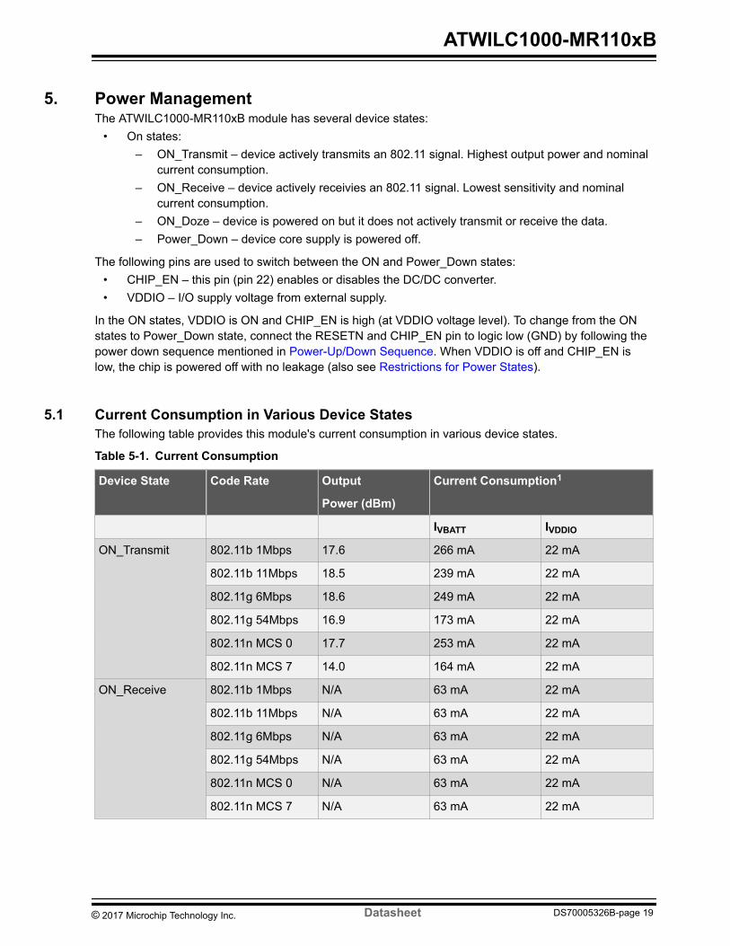
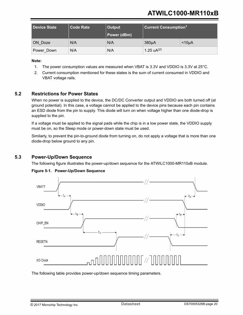
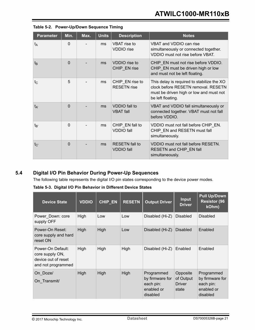
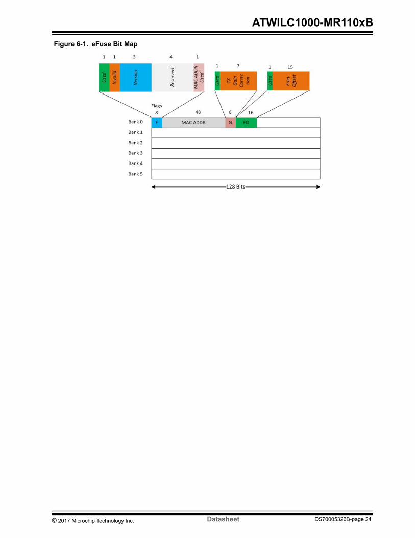
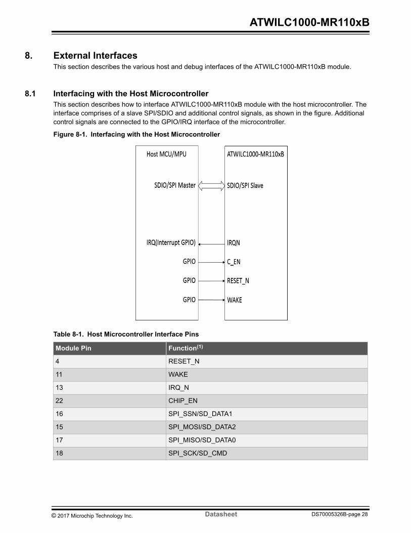
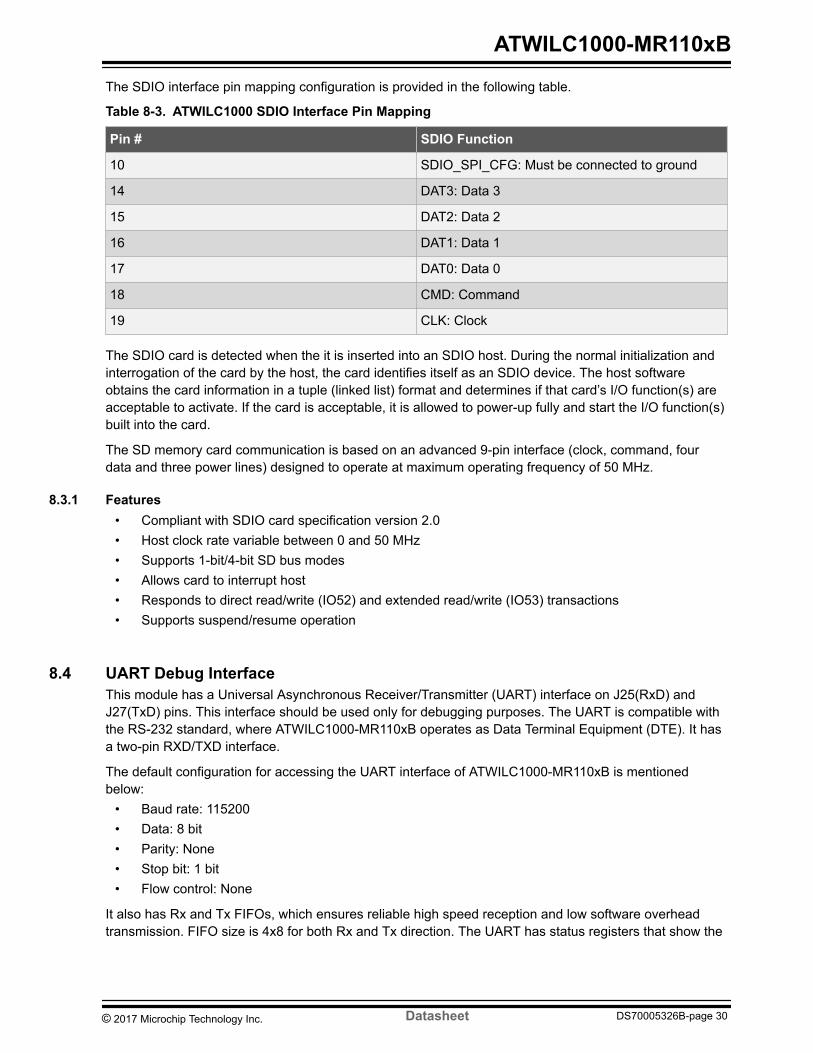
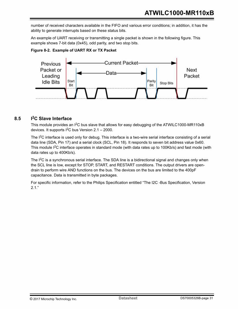
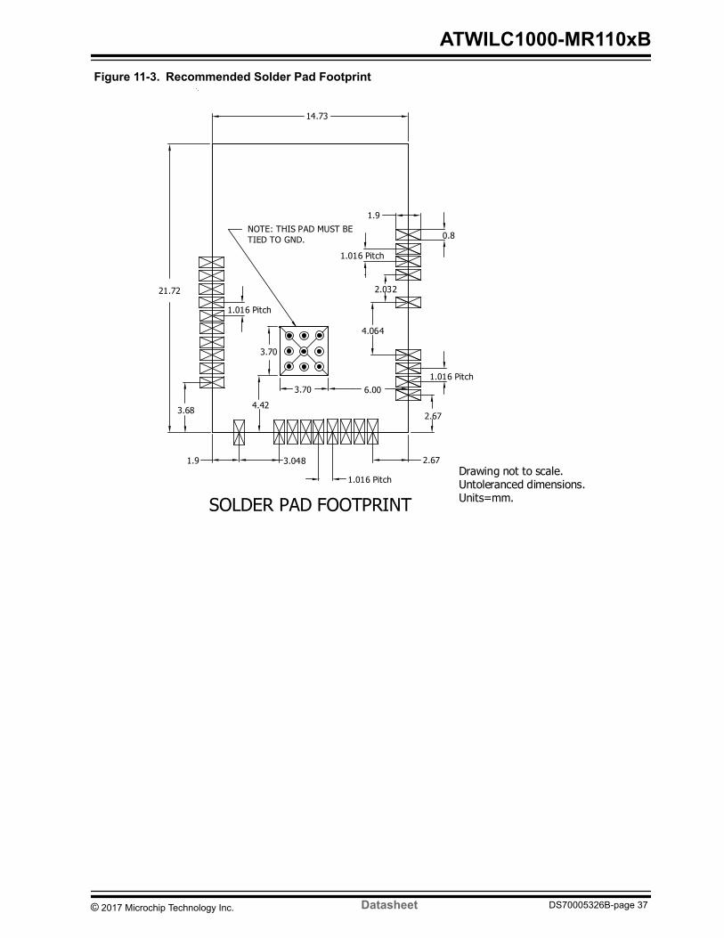
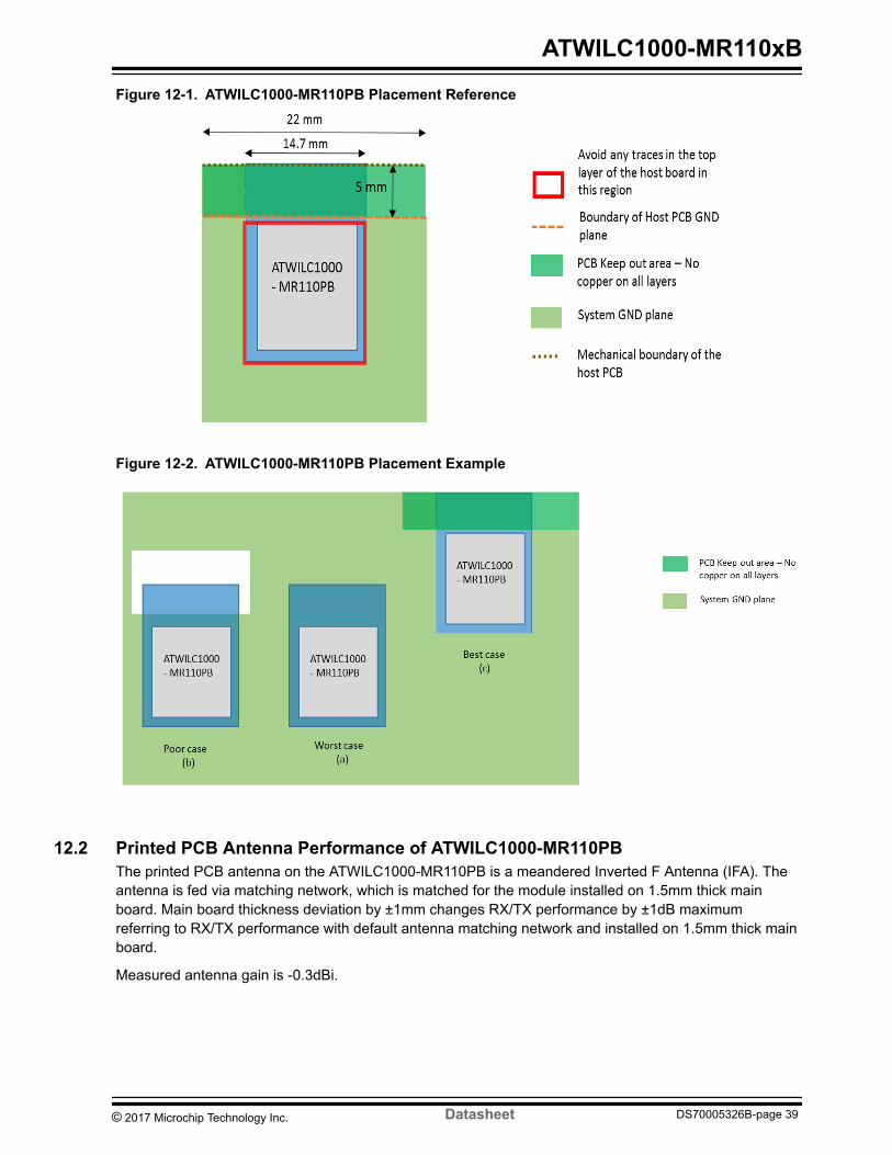
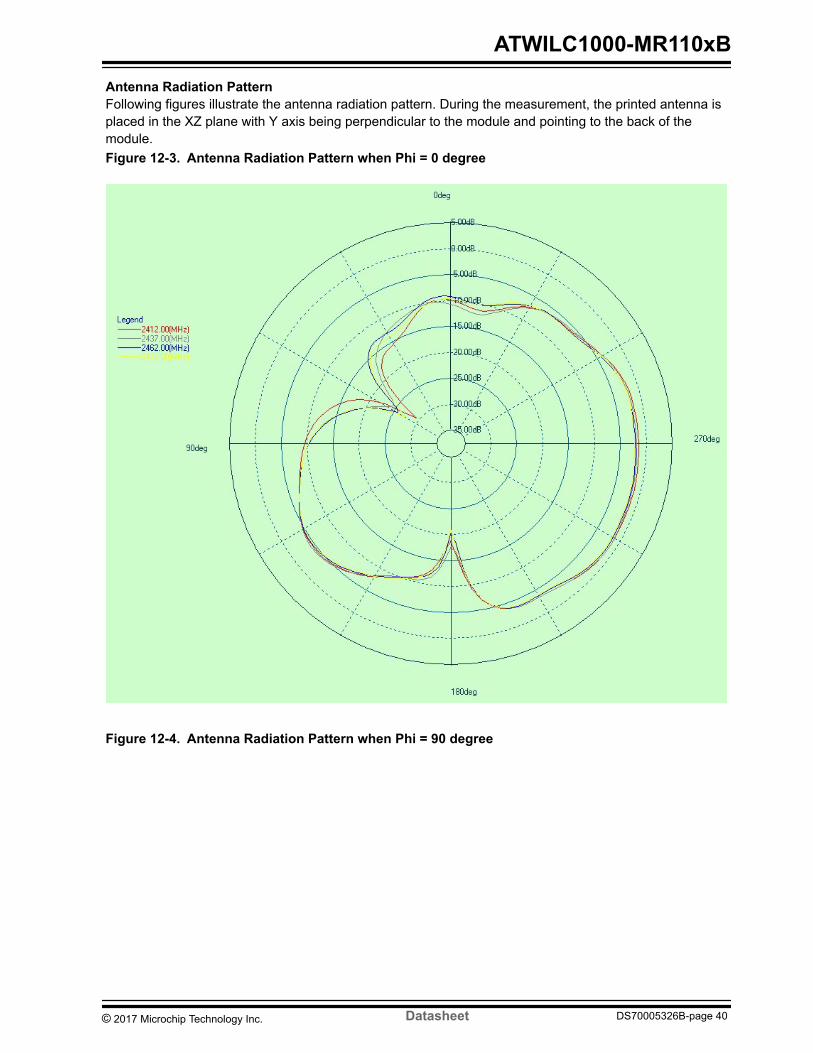
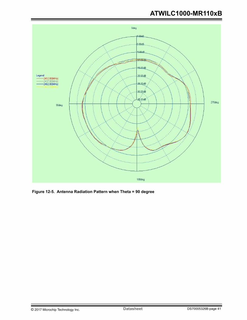
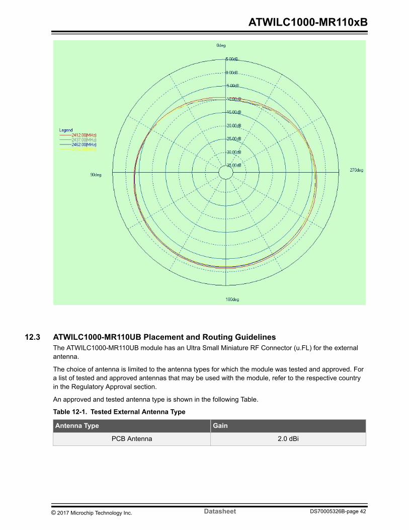
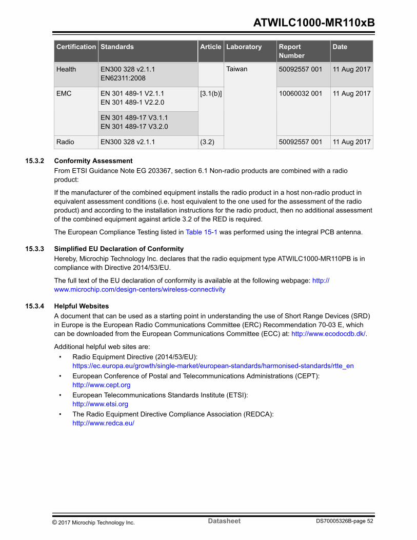
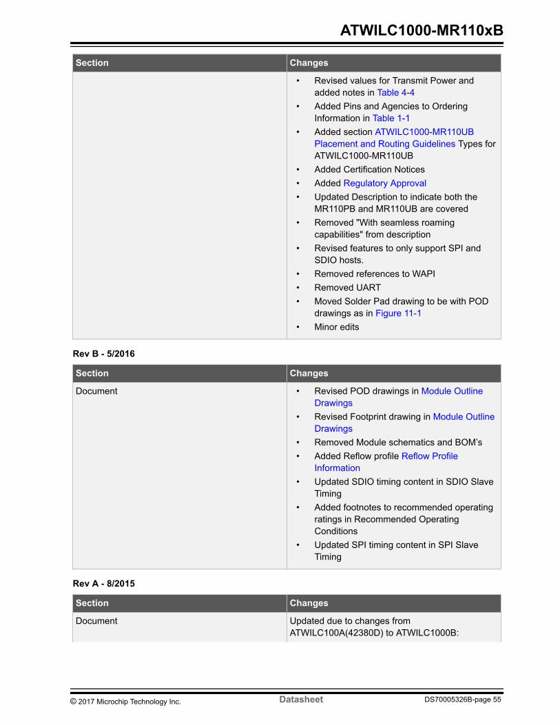
Section Changes
bull Revised values for Transmit Power andadded notes in Table 4-4
bull Added Pins and Agencies to OrderingInformation in Table 1-1
bull Added section ATWILC1000-MR110UBPlacement and Routing Guidelines Types forATWILC1000-MR110UB
bull Added Certification Noticesbull Added Regulatory Approvalbull Updated Description to indicate both the
MR110PB and MR110UB are coveredbull Removed With seamless roaming
capabilities from descriptionbull Revised features to only support SPI and
SDIO hostsbull Removed references to WAPIbull Removed UARTbull Moved Solder Pad drawing to be with POD
drawings as in Figure 11-1bull Minor edits
Rev B - 52016
Section Changes
Document bull Revised POD drawings in Module OutlineDrawings
bull Revised Footprint drawing in Module OutlineDrawings
bull Removed Module schematics and BOMrsquosbull Added Reflow profile Reflow Profile
Informationbull Updated SDIO timing content in SDIO Slave
Timingbull Added footnotes to recommended operating
ratings in Recommended OperatingConditions
bull Updated SPI timing content in SPI SlaveTiming
Rev A - 82015
Section Changes
Document Updated due to changes fromATWILC100A(42380D) to ATWILC1000B
ATWILC1000-MR110xB
copy 2017 Microchip Technology Inc Datasheet DS70005326B-page 55
Section Changes
bull Updated power numbers and descriptionadded high-power and low-power modes
bull Updated radio performance numbersbull Fixed typos in SPI interface timingbull Added hardware accelerators in feature list
(security and checksum)bull Increased instruction RAM size from 128KB
to 160KBbull Improved and corrected description of
Coexistence interfacebull Miscellaneous minor updates and
corrections
ATWILC1000-MR110xB
copy 2017 Microchip Technology Inc Datasheet DS70005326B-page 56
The Microchip Web Site
Microchip provides online support via our web site at httpwwwmicrochipcom This web site is used asa means to make files and information easily available to customers Accessible by using your favoriteInternet browser the web site contains the following information
bull Product Support ndash Data sheets and errata application notes and sample programs designresources userrsquos guides and hardware support documents latest software releases and archivedsoftware
bull General Technical Support ndash Frequently Asked Questions (FAQ) technical support requestsonline discussion groups Microchip consultant program member listing
bull Business of Microchip ndash Product selector and ordering guides latest Microchip press releaseslisting of seminars and events listings of Microchip sales offices distributors and factoryrepresentatives
Customer Change Notification Service
Microchiprsquos customer notification service helps keep customers current on Microchip productsSubscribers will receive e-mail notification whenever there are changes updates revisions or erratarelated to a specified product family or development tool of interest
To register access the Microchip web site at httpwwwmicrochipcom Under ldquoSupportrdquo click onldquoCustomer Change Notificationrdquo and follow the registration instructions
Customer Support
Users of Microchip products can receive assistance through several channels
bull Distributor or Representativebull Local Sales Officebull Field Application Engineer (FAE)bull Technical Support
Customers should contact their distributor representative or Field Application Engineer (FAE) for supportLocal sales offices are also available to help customers A listing of sales offices and locations is includedin the back of this document
Technical support is available through the web site at httpwwwmicrochipcomsupport
Microchip Devices Code Protection Feature
Note the following details of the code protection feature on Microchip devices
bull Microchip products meet the specification contained in their particular Microchip Data Sheetbull Microchip believes that its family of products is one of the most secure families of its kind on the
market today when used in the intended manner and under normal conditionsbull There are dishonest and possibly illegal methods used to breach the code protection feature All of
these methods to our knowledge require using the Microchip products in a manner outside theoperating specifications contained in Microchiprsquos Data Sheets Most likely the person doing so isengaged in theft of intellectual property
bull Microchip is willing to work with the customer who is concerned about the integrity of their code
ATWILC1000-MR110xB
copy 2017 Microchip Technology Inc Datasheet DS70005326B-page 57
bull Neither Microchip nor any other semiconductor manufacturer can guarantee the security of theircode Code protection does not mean that we are guaranteeing the product as ldquounbreakablerdquo
Code protection is constantly evolving We at Microchip are committed to continuously improving thecode protection features of our products Attempts to break Microchiprsquos code protection feature may be aviolation of the Digital Millennium Copyright Act If such acts allow unauthorized access to your softwareor other copyrighted work you may have a right to sue for relief under that Act
Legal NoticeInformation contained in this publication regarding device applications and the like is provided only foryour convenience and may be superseded by updates It is your responsibility to ensure that yourapplication meets with your specifications MICROCHIP MAKES NO REPRESENTATIONS ORWARRANTIES OF ANY KIND WHETHER EXPRESS OR IMPLIED WRITTEN OR ORAL STATUTORYOR OTHERWISE RELATED TO THE INFORMATION INCLUDING BUT NOT LIMITED TO ITSCONDITION QUALITY PERFORMANCE MERCHANTABILITY OR FITNESS FOR PURPOSEMicrochip disclaims all liability arising from this information and its use Use of Microchip devices in lifesupport andor safety applications is entirely at the buyerrsquos risk and the buyer agrees to defendindemnify and hold harmless Microchip from any and all damages claims suits or expenses resultingfrom such use No licenses are conveyed implicitly or otherwise under any Microchip intellectualproperty rights unless otherwise stated
TrademarksThe Microchip name and logo the Microchip logo AnyRate AVR AVR logo AVR Freaks BeaconThingsBitCloud CryptoMemory CryptoRF dsPIC FlashFlex flexPWR Heldo JukeBlox KeeLoq KeeLoq logoKleer LANCheck LINK MD maXStylus maXTouch MediaLB megaAVR MOST MOST logo MPLABOptoLyzer PIC picoPower PICSTART PIC32 logo Prochip Designer QTouch RightTouch SAM-BASpyNIC SST SST Logo SuperFlash tinyAVR UNIO and XMEGA are registered trademarks ofMicrochip Technology Incorporated in the USA and other countries
ClockWorks The Embedded Control Solutions Company EtherSynch Hyper Speed Control HyperLightLoad IntelliMOS mTouch Precision Edge and Quiet-Wire are registered trademarks of MicrochipTechnology Incorporated in the USA
Adjacent Key Suppression AKS Analog-for-the-Digital Age Any Capacitor AnyIn AnyOut BodyComchipKIT chipKIT logo CodeGuard CryptoAuthentication CryptoCompanion CryptoControllerdsPICDEM dsPICDEMnet Dynamic Average Matching DAM ECAN EtherGREEN In-Circuit SerialProgramming ICSP Inter-Chip Connectivity JitterBlocker KleerNet KleerNet logo Mindi MiWimotorBench MPASM MPF MPLAB Certified logo MPLIB MPLINK MultiTRAK NetDetach OmniscientCode Generation PICDEM PICDEMnet PICkit PICtail PureSilicon QMatrix RightTouch logo REALICE Ripple Blocker SAM-ICE Serial Quad IO SMART-IS SQI SuperSwitcher SuperSwitcher II TotalEndurance TSHARC USBCheck VariSense ViewSpan WiperLock Wireless DNA and ZENA aretrademarks of Microchip Technology Incorporated in the USA and other countries
SQTP is a service mark of Microchip Technology Incorporated in the USA
Silicon Storage Technology is a registered trademark of Microchip Technology Inc in other countries
GestIC is a registered trademark of Microchip Technology Germany II GmbH amp Co KG a subsidiary ofMicrochip Technology Inc in other countries
All other trademarks mentioned herein are property of their respective companiescopy 2017 Microchip Technology Incorporated Printed in the USA All Rights Reserved
ATWILC1000-MR110xB
copy 2017 Microchip Technology Inc Datasheet DS70005326B-page 58
ISBN 978-1-5224-2223-5
Quality Management System Certified by DNV
ISOTS 16949Microchip received ISOTS-169492009 certification for its worldwide headquarters design and waferfabrication facilities in Chandler and Tempe Arizona Gresham Oregon and design centers in Californiaand India The Companyrsquos quality system processes and procedures are for its PICreg MCUs and dsPICreg
DSCs KEELOQreg code hopping devices Serial EEPROMs microperipherals nonvolatile memory andanalog products In addition Microchiprsquos quality system for the design and manufacture of developmentsystems is ISO 90012000 certified
ATWILC1000-MR110xB
copy 2017 Microchip Technology Inc Datasheet DS70005326B-page 59
AMERICAS ASIAPACIFIC ASIAPACIFIC EUROPECorporate Office2355 West Chandler BlvdChandler AZ 85224-6199Tel 480-792-7200Fax 480-792-7277Technical SupporthttpwwwmicrochipcomsupportWeb AddresswwwmicrochipcomAtlantaDuluth GATel 678-957-9614Fax 678-957-1455Austin TXTel 512-257-3370BostonWestborough MATel 774-760-0087Fax 774-760-0088ChicagoItasca ILTel 630-285-0071Fax 630-285-0075DallasAddison TXTel 972-818-7423Fax 972-818-2924DetroitNovi MITel 248-848-4000Houston TXTel 281-894-5983IndianapolisNoblesville INTel 317-773-8323Fax 317-773-5453Tel 317-536-2380Los AngelesMission Viejo CATel 949-462-9523Fax 949-462-9608Tel 951-273-7800Raleigh NCTel 919-844-7510New York NYTel 631-435-6000San Jose CATel 408-735-9110Tel 408-436-4270Canada - TorontoTel 905-695-1980Fax 905-695-2078
Asia Pacific OfficeSuites 3707-14 37th FloorTower 6 The GatewayHarbour City KowloonHong KongTel 852-2943-5100Fax 852-2401-3431Australia - SydneyTel 61-2-9868-6733Fax 61-2-9868-6755China - BeijingTel 86-10-8569-7000Fax 86-10-8528-2104China - ChengduTel 86-28-8665-5511Fax 86-28-8665-7889China - ChongqingTel 86-23-8980-9588Fax 86-23-8980-9500China - DongguanTel 86-769-8702-9880China - GuangzhouTel 86-20-8755-8029China - HangzhouTel 86-571-8792-8115Fax 86-571-8792-8116China - Hong Kong SARTel 852-2943-5100Fax 852-2401-3431China - NanjingTel 86-25-8473-2460Fax 86-25-8473-2470China - QingdaoTel 86-532-8502-7355Fax 86-532-8502-7205China - ShanghaiTel 86-21-3326-8000Fax 86-21-3326-8021China - ShenyangTel 86-24-2334-2829Fax 86-24-2334-2393China - ShenzhenTel 86-755-8864-2200Fax 86-755-8203-1760China - WuhanTel 86-27-5980-5300Fax 86-27-5980-5118China - XianTel 86-29-8833-7252Fax 86-29-8833-7256
China - XiamenTel 86-592-2388138Fax 86-592-2388130China - ZhuhaiTel 86-756-3210040Fax 86-756-3210049India - BangaloreTel 91-80-3090-4444Fax 91-80-3090-4123India - New DelhiTel 91-11-4160-8631Fax 91-11-4160-8632India - PuneTel 91-20-3019-1500Japan - OsakaTel 81-6-6152-7160Fax 81-6-6152-9310Japan - TokyoTel 81-3-6880- 3770Fax 81-3-6880-3771Korea - DaeguTel 82-53-744-4301Fax 82-53-744-4302Korea - SeoulTel 82-2-554-7200Fax 82-2-558-5932 or82-2-558-5934Malaysia - Kuala LumpurTel 60-3-6201-9857Fax 60-3-6201-9859Malaysia - PenangTel 60-4-227-8870Fax 60-4-227-4068Philippines - ManilaTel 63-2-634-9065Fax 63-2-634-9069SingaporeTel 65-6334-8870Fax 65-6334-8850Taiwan - Hsin ChuTel 886-3-5778-366Fax 886-3-5770-955Taiwan - KaohsiungTel 886-7-213-7830Taiwan - TaipeiTel 886-2-2508-8600Fax 886-2-2508-0102Thailand - BangkokTel 66-2-694-1351Fax 66-2-694-1350
Austria - WelsTel 43-7242-2244-39Fax 43-7242-2244-393Denmark - CopenhagenTel 45-4450-2828Fax 45-4485-2829Finland - EspooTel 358-9-4520-820France - ParisTel 33-1-69-53-63-20Fax 33-1-69-30-90-79France - Saint CloudTel 33-1-30-60-70-00Germany - GarchingTel 49-8931-9700Germany - HaanTel 49-2129-3766400Germany - HeilbronnTel 49-7131-67-3636Germany - KarlsruheTel 49-721-625370Germany - MunichTel 49-89-627-144-0Fax 49-89-627-144-44Germany - RosenheimTel 49-8031-354-560Israel - RarsquoananaTel 972-9-744-7705Italy - MilanTel 39-0331-742611Fax 39-0331-466781Italy - PadovaTel 39-049-7625286Netherlands - DrunenTel 31-416-690399Fax 31-416-690340Norway - TrondheimTel 47-7289-7561Poland - WarsawTel 48-22-3325737Romania - BucharestTel 40-21-407-87-50Spain - MadridTel 34-91-708-08-90Fax 34-91-708-08-91Sweden - GothenbergTel 46-31-704-60-40Sweden - StockholmTel 46-8-5090-4654UK - WokinghamTel 44-118-921-5800Fax 44-118-921-5820
Worldwide Sales and Service
copy 2017 Microchip Technology Inc Datasheet DS70005326B-page 60
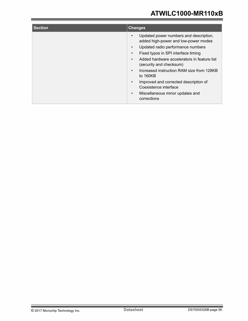
Section Changes
bull Updated power numbers and descriptionadded high-power and low-power modes
bull Updated radio performance numbersbull Fixed typos in SPI interface timingbull Added hardware accelerators in feature list
(security and checksum)bull Increased instruction RAM size from 128KB
to 160KBbull Improved and corrected description of
Coexistence interfacebull Miscellaneous minor updates and
corrections
ATWILC1000-MR110xB
copy 2017 Microchip Technology Inc Datasheet DS70005326B-page 56
The Microchip Web Site
Microchip provides online support via our web site at httpwwwmicrochipcom This web site is used asa means to make files and information easily available to customers Accessible by using your favoriteInternet browser the web site contains the following information
bull Product Support ndash Data sheets and errata application notes and sample programs designresources userrsquos guides and hardware support documents latest software releases and archivedsoftware
bull General Technical Support ndash Frequently Asked Questions (FAQ) technical support requestsonline discussion groups Microchip consultant program member listing
bull Business of Microchip ndash Product selector and ordering guides latest Microchip press releaseslisting of seminars and events listings of Microchip sales offices distributors and factoryrepresentatives
Customer Change Notification Service
Microchiprsquos customer notification service helps keep customers current on Microchip productsSubscribers will receive e-mail notification whenever there are changes updates revisions or erratarelated to a specified product family or development tool of interest
To register access the Microchip web site at httpwwwmicrochipcom Under ldquoSupportrdquo click onldquoCustomer Change Notificationrdquo and follow the registration instructions
Customer Support
Users of Microchip products can receive assistance through several channels
bull Distributor or Representativebull Local Sales Officebull Field Application Engineer (FAE)bull Technical Support
Customers should contact their distributor representative or Field Application Engineer (FAE) for supportLocal sales offices are also available to help customers A listing of sales offices and locations is includedin the back of this document
Technical support is available through the web site at httpwwwmicrochipcomsupport
Microchip Devices Code Protection Feature
Note the following details of the code protection feature on Microchip devices
bull Microchip products meet the specification contained in their particular Microchip Data Sheetbull Microchip believes that its family of products is one of the most secure families of its kind on the
market today when used in the intended manner and under normal conditionsbull There are dishonest and possibly illegal methods used to breach the code protection feature All of
these methods to our knowledge require using the Microchip products in a manner outside theoperating specifications contained in Microchiprsquos Data Sheets Most likely the person doing so isengaged in theft of intellectual property
bull Microchip is willing to work with the customer who is concerned about the integrity of their code
ATWILC1000-MR110xB
copy 2017 Microchip Technology Inc Datasheet DS70005326B-page 57
bull Neither Microchip nor any other semiconductor manufacturer can guarantee the security of theircode Code protection does not mean that we are guaranteeing the product as ldquounbreakablerdquo
Code protection is constantly evolving We at Microchip are committed to continuously improving thecode protection features of our products Attempts to break Microchiprsquos code protection feature may be aviolation of the Digital Millennium Copyright Act If such acts allow unauthorized access to your softwareor other copyrighted work you may have a right to sue for relief under that Act
Legal NoticeInformation contained in this publication regarding device applications and the like is provided only foryour convenience and may be superseded by updates It is your responsibility to ensure that yourapplication meets with your specifications MICROCHIP MAKES NO REPRESENTATIONS ORWARRANTIES OF ANY KIND WHETHER EXPRESS OR IMPLIED WRITTEN OR ORAL STATUTORYOR OTHERWISE RELATED TO THE INFORMATION INCLUDING BUT NOT LIMITED TO ITSCONDITION QUALITY PERFORMANCE MERCHANTABILITY OR FITNESS FOR PURPOSEMicrochip disclaims all liability arising from this information and its use Use of Microchip devices in lifesupport andor safety applications is entirely at the buyerrsquos risk and the buyer agrees to defendindemnify and hold harmless Microchip from any and all damages claims suits or expenses resultingfrom such use No licenses are conveyed implicitly or otherwise under any Microchip intellectualproperty rights unless otherwise stated
TrademarksThe Microchip name and logo the Microchip logo AnyRate AVR AVR logo AVR Freaks BeaconThingsBitCloud CryptoMemory CryptoRF dsPIC FlashFlex flexPWR Heldo JukeBlox KeeLoq KeeLoq logoKleer LANCheck LINK MD maXStylus maXTouch MediaLB megaAVR MOST MOST logo MPLABOptoLyzer PIC picoPower PICSTART PIC32 logo Prochip Designer QTouch RightTouch SAM-BASpyNIC SST SST Logo SuperFlash tinyAVR UNIO and XMEGA are registered trademarks ofMicrochip Technology Incorporated in the USA and other countries
ClockWorks The Embedded Control Solutions Company EtherSynch Hyper Speed Control HyperLightLoad IntelliMOS mTouch Precision Edge and Quiet-Wire are registered trademarks of MicrochipTechnology Incorporated in the USA
Adjacent Key Suppression AKS Analog-for-the-Digital Age Any Capacitor AnyIn AnyOut BodyComchipKIT chipKIT logo CodeGuard CryptoAuthentication CryptoCompanion CryptoControllerdsPICDEM dsPICDEMnet Dynamic Average Matching DAM ECAN EtherGREEN In-Circuit SerialProgramming ICSP Inter-Chip Connectivity JitterBlocker KleerNet KleerNet logo Mindi MiWimotorBench MPASM MPF MPLAB Certified logo MPLIB MPLINK MultiTRAK NetDetach OmniscientCode Generation PICDEM PICDEMnet PICkit PICtail PureSilicon QMatrix RightTouch logo REALICE Ripple Blocker SAM-ICE Serial Quad IO SMART-IS SQI SuperSwitcher SuperSwitcher II TotalEndurance TSHARC USBCheck VariSense ViewSpan WiperLock Wireless DNA and ZENA aretrademarks of Microchip Technology Incorporated in the USA and other countries
SQTP is a service mark of Microchip Technology Incorporated in the USA
Silicon Storage Technology is a registered trademark of Microchip Technology Inc in other countries
GestIC is a registered trademark of Microchip Technology Germany II GmbH amp Co KG a subsidiary ofMicrochip Technology Inc in other countries
All other trademarks mentioned herein are property of their respective companiescopy 2017 Microchip Technology Incorporated Printed in the USA All Rights Reserved
ATWILC1000-MR110xB
copy 2017 Microchip Technology Inc Datasheet DS70005326B-page 58
ISBN 978-1-5224-2223-5
Quality Management System Certified by DNV
ISOTS 16949Microchip received ISOTS-169492009 certification for its worldwide headquarters design and waferfabrication facilities in Chandler and Tempe Arizona Gresham Oregon and design centers in Californiaand India The Companyrsquos quality system processes and procedures are for its PICreg MCUs and dsPICreg
DSCs KEELOQreg code hopping devices Serial EEPROMs microperipherals nonvolatile memory andanalog products In addition Microchiprsquos quality system for the design and manufacture of developmentsystems is ISO 90012000 certified
ATWILC1000-MR110xB
copy 2017 Microchip Technology Inc Datasheet DS70005326B-page 59
AMERICAS ASIAPACIFIC ASIAPACIFIC EUROPECorporate Office2355 West Chandler BlvdChandler AZ 85224-6199Tel 480-792-7200Fax 480-792-7277Technical SupporthttpwwwmicrochipcomsupportWeb AddresswwwmicrochipcomAtlantaDuluth GATel 678-957-9614Fax 678-957-1455Austin TXTel 512-257-3370BostonWestborough MATel 774-760-0087Fax 774-760-0088ChicagoItasca ILTel 630-285-0071Fax 630-285-0075DallasAddison TXTel 972-818-7423Fax 972-818-2924DetroitNovi MITel 248-848-4000Houston TXTel 281-894-5983IndianapolisNoblesville INTel 317-773-8323Fax 317-773-5453Tel 317-536-2380Los AngelesMission Viejo CATel 949-462-9523Fax 949-462-9608Tel 951-273-7800Raleigh NCTel 919-844-7510New York NYTel 631-435-6000San Jose CATel 408-735-9110Tel 408-436-4270Canada - TorontoTel 905-695-1980Fax 905-695-2078
Asia Pacific OfficeSuites 3707-14 37th FloorTower 6 The GatewayHarbour City KowloonHong KongTel 852-2943-5100Fax 852-2401-3431Australia - SydneyTel 61-2-9868-6733Fax 61-2-9868-6755China - BeijingTel 86-10-8569-7000Fax 86-10-8528-2104China - ChengduTel 86-28-8665-5511Fax 86-28-8665-7889China - ChongqingTel 86-23-8980-9588Fax 86-23-8980-9500China - DongguanTel 86-769-8702-9880China - GuangzhouTel 86-20-8755-8029China - HangzhouTel 86-571-8792-8115Fax 86-571-8792-8116China - Hong Kong SARTel 852-2943-5100Fax 852-2401-3431China - NanjingTel 86-25-8473-2460Fax 86-25-8473-2470China - QingdaoTel 86-532-8502-7355Fax 86-532-8502-7205China - ShanghaiTel 86-21-3326-8000Fax 86-21-3326-8021China - ShenyangTel 86-24-2334-2829Fax 86-24-2334-2393China - ShenzhenTel 86-755-8864-2200Fax 86-755-8203-1760China - WuhanTel 86-27-5980-5300Fax 86-27-5980-5118China - XianTel 86-29-8833-7252Fax 86-29-8833-7256
China - XiamenTel 86-592-2388138Fax 86-592-2388130China - ZhuhaiTel 86-756-3210040Fax 86-756-3210049India - BangaloreTel 91-80-3090-4444Fax 91-80-3090-4123India - New DelhiTel 91-11-4160-8631Fax 91-11-4160-8632India - PuneTel 91-20-3019-1500Japan - OsakaTel 81-6-6152-7160Fax 81-6-6152-9310Japan - TokyoTel 81-3-6880- 3770Fax 81-3-6880-3771Korea - DaeguTel 82-53-744-4301Fax 82-53-744-4302Korea - SeoulTel 82-2-554-7200Fax 82-2-558-5932 or82-2-558-5934Malaysia - Kuala LumpurTel 60-3-6201-9857Fax 60-3-6201-9859Malaysia - PenangTel 60-4-227-8870Fax 60-4-227-4068Philippines - ManilaTel 63-2-634-9065Fax 63-2-634-9069SingaporeTel 65-6334-8870Fax 65-6334-8850Taiwan - Hsin ChuTel 886-3-5778-366Fax 886-3-5770-955Taiwan - KaohsiungTel 886-7-213-7830Taiwan - TaipeiTel 886-2-2508-8600Fax 886-2-2508-0102Thailand - BangkokTel 66-2-694-1351Fax 66-2-694-1350
Austria - WelsTel 43-7242-2244-39Fax 43-7242-2244-393Denmark - CopenhagenTel 45-4450-2828Fax 45-4485-2829Finland - EspooTel 358-9-4520-820France - ParisTel 33-1-69-53-63-20Fax 33-1-69-30-90-79France - Saint CloudTel 33-1-30-60-70-00Germany - GarchingTel 49-8931-9700Germany - HaanTel 49-2129-3766400Germany - HeilbronnTel 49-7131-67-3636Germany - KarlsruheTel 49-721-625370Germany - MunichTel 49-89-627-144-0Fax 49-89-627-144-44Germany - RosenheimTel 49-8031-354-560Israel - RarsquoananaTel 972-9-744-7705Italy - MilanTel 39-0331-742611Fax 39-0331-466781Italy - PadovaTel 39-049-7625286Netherlands - DrunenTel 31-416-690399Fax 31-416-690340Norway - TrondheimTel 47-7289-7561Poland - WarsawTel 48-22-3325737Romania - BucharestTel 40-21-407-87-50Spain - MadridTel 34-91-708-08-90Fax 34-91-708-08-91Sweden - GothenbergTel 46-31-704-60-40Sweden - StockholmTel 46-8-5090-4654UK - WokinghamTel 44-118-921-5800Fax 44-118-921-5820
Worldwide Sales and Service
copy 2017 Microchip Technology Inc Datasheet DS70005326B-page 60