Embed Size (px)
Citation preview
IEEE JOURNAL OF EMERGING AND SELECTED TOPICS IN POWER ELECTRONICS, VOL. 4, NO. 3, SEPTEMBER 2016 757
Electromagnetic Interference Simulations forWide-Bandgap Power Electronic Modules
Atanu Dutta, Student Member, IEEE, and Simon S. Ang, Fellow, IEEE
Abstract— A simulation methodology that incorporates cosim-ulation techniques using ANSYS EM tools is proposed to predictradiated and conducted electromagnetic interference (EMI) frompower electronic modules. The radiated EMIs for a coplanar wirebonded and wire bondless power electronic modules are simu-lated and compared. The instantaneous power-levels conductingthrough the power devices in the wire bonded power moduleare significantly higher than those for the wire bondless powerelectronic module due to parasitic circuit element imbalance.These power-levels occur for a very short duration at the turn-ONand turn-OFF of the devices and can be considered as a potentialsource of radiated EMI emissions. Through the cosimulation tech-nique, it is shown that the wire bondless power electronic modulehas a better electromagnetic compatibility (EMC) compliancecompared with that of the coplanar wire bonded power electronicmodule. Conducted EMI measurements and simulations are alsoperformed to predict the conducted EMI and validate the simu-lation methodology. The proposed cosimulation technique can beimplemented during the initial design phase of power modules toreduce significant time to physically test module-level EMC/EMI.
Index Terms— Electromagnetic interference (EMI), powerelectronic modules, simulation methodology.
I. INTRODUCTION
FAST switching, power dense, and compact power elec-tronic modules or power modules are in great demand
for modern power electronic systems. In these power modules,wide-bandgap power semiconductor devices, such as siliconcarbide (SiC) and gallium nitride, are increasingly being usedfor efficient fast switching and continuous operation at hightemperatures. Recently, many research efforts are focused tounderstand the characteristics of these devices as well asutilize these fast switching devices in high power densitymodules for various applications [1]–[12]. Because of thehigh dv/dt and di/dt slew rates in these wide-bandgap powersemiconductor devices, they generate significant electromag-netic compatibility (EMC) concerns [13]–[15]. As such, it isnecessary in the early design phase of these power modulesto address electromagnetic interference (EMI). Mitigation ofEMI in power converters using improved layout techniques has
Manuscript received January 10, 2016; revised March 13, 2016; acceptedMay 4, 2016. Date of publication May 26, 2016; date of current versionJuly 29, 2016. This work was supported in part by the U.S. NationalScience Foundation within the Industry/University Cooperative ResearchCentre on Grid-Connected Advanced Power Electronic Systems underGrant IIP-1439700. Recommended for publication by AssociateEditor J. Biela.
The authors are with the Department of Electrical Engineering, Universityof Arkansas, Fayetteville, AR 72701 USA (e-mail: [email protected];[email protected]).
Color versions of one or more of the figures in this paper are availableonline at http://ieeexplore.ieee.org.
Digital Object Identifier 10.1109/JESTPE.2016.2573315
been discussed in [13] and [16]–[18]. Various mathematicaland numerical modeling approaches have been reported tounderstand EMI sources and generation mechanisms to predictboth conducted and radiated EMI in power convert systemsin [29]–[33]. However, their approaches are limited by overlysimplified device models and circuit approximations, whicheventually prevent precise prediction of EMI. The simulationmethodology proposed in this paper directly addresses bothradiated and conducted EMI, taking into consideration thenonideal transient characteristics during the switching oper-ation and corresponding power-levels through each device.Typically, the EMI/EMC test for the power module is per-formed after the physical prototyping of the power modulein an anechoic chamber [14]. Physical prototyping of thepower modules to test for EMI issues can be a very longand costly engineering process. As such, a coherent simulationmethodology to predict the EMI issues early in the designprocess is desired. In this paper, a simulation methodology thatincorporates cosimulation techniques using ANSYS EM toolsis proposed to predict the radiated and conducted EMI. Theproposed simulation methodology is validated using radiatedand conducted EMI measurements using a simple near-fieldmeasurement technique with near-field EM probes and lineimpedance stabilization network (LISN).
The magnitude of the current conducting throughthe physical traces during switching operation, parasiticcircuit elements, and physical characteristics of the powersemiconductor devices are important parameters that governthe switching characteristics of the power device [19], [20].These parameters are also important considerations to predictthe EMI in a power module. The proposed simulation method-ology commences with a static current conduction simulationon the power module layout using ANSYS MAXWELL [26].Subsequently, a frequency-dependent parasitic extractionof the physical traces on the power module is performedusing ANSYS Q3D extractor [28]. The frequency-dependentparasitic model is then dynamically linked to ANSYSSIMPLORER. Using physical model characteristics fromdevice manufacturer’s data sheet, the electrical characteristicsof the power semiconductor device are reproduced usingANSYS SIMPLORER’s built-in semiconductor devicecharacterization tool [27]. A frequency-dependent parasiticmodel-based circuit schematic of the power module is thenconstructed. From ANSYS SIMPLORER, the waveformsfrom transient simulations are then imported to ANSYS HighFrequency Structure Simulator (HFSS) [28] to perform afull-wave 3-D EM field simulation to analyze the radiated
2168-6777 © 2016 IEEE. Personal use is permitted, but republication/redistribution requires IEEE permission.See http://www.ieee.org/publications_standards/publications/rights/index.html for more information.
758 IEEE JOURNAL OF EMERGING AND SELECTED TOPICS IN POWER ELECTRONICS, VOL. 4, NO. 3, SEPTEMBER 2016
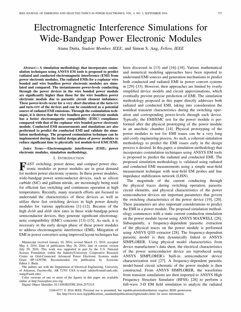
Fig. 1. Flowchart of the simulation methodology.
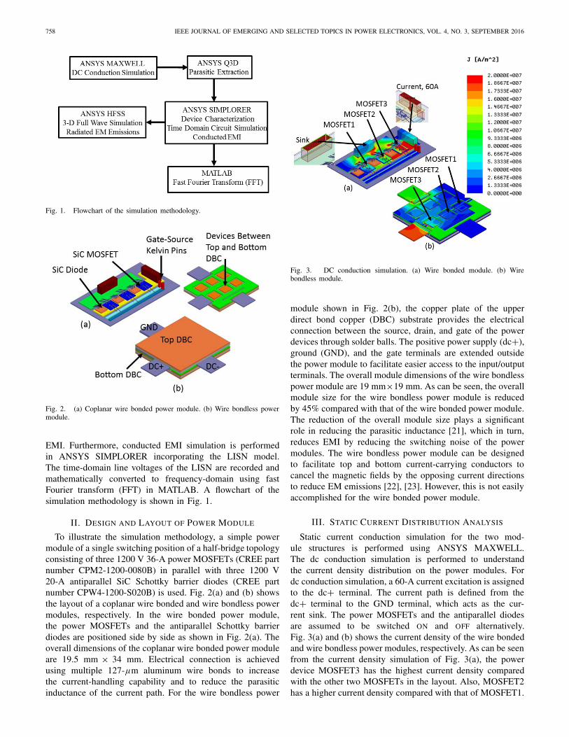
Fig. 2. (a) Coplanar wire bonded power module. (b) Wire bondless powermodule.
EMI. Furthermore, conducted EMI simulation is performedin ANSYS SIMPLORER incorporating the LISN model.The time-domain line voltages of the LISN are recorded andmathematically converted to frequency-domain using fastFourier transform (FFT) in MATLAB. A flowchart of thesimulation methodology is shown in Fig. 1.
II. DESIGN AND LAYOUT OF POWER MODULE
To illustrate the simulation methodology, a simple powermodule of a single switching position of a half-bridge topologyconsisting of three 1200 V 36-A power MOSFETs (CREE partnumber CPM2-1200-0080B) in parallel with three 1200 V20-A antiparallel SiC Schottky barrier diodes (CREE partnumber CPW4-1200-S020B) is used. Fig. 2(a) and (b) showsthe layout of a coplanar wire bonded and wire bondless powermodules, respectively. In the wire bonded power module,the power MOSFETs and the antiparallel Schottky barrierdiodes are positioned side by side as shown in Fig. 2(a). Theoverall dimensions of the coplanar wire bonded power moduleare 19.5 mm × 34 mm. Electrical connection is achievedusing multiple 127-μm aluminum wire bonds to increasethe current-handling capability and to reduce the parasiticinductance of the current path. For the wire bondless power
Fig. 3. DC conduction simulation. (a) Wire bonded module. (b) Wirebondless module.
module shown in Fig. 2(b), the copper plate of the upperdirect bond copper (DBC) substrate provides the electricalconnection between the source, drain, and gate of the powerdevices through solder balls. The positive power supply (dc+),ground (GND), and the gate terminals are extended outsidethe power module to facilitate easier access to the input/outputterminals. The overall module dimensions of the wire bondlesspower module are 19 mm×19 mm. As can be seen, the overallmodule size for the wire bondless power module is reducedby 45% compared with that of the wire bonded power module.The reduction of the overall module size plays a significantrole in reducing the parasitic inductance [21], which in turn,reduces EMI by reducing the switching noise of the powermodules. The wire bondless power module can be designedto facilitate top and bottom current-carrying conductors tocancel the magnetic fields by the opposing current directionsto reduce EM emissions [22], [23]. However, this is not easilyaccomplished for the wire bonded power module.
III. STATIC CURRENT DISTRIBUTION ANALYSIS
Static current conduction simulation for the two mod-ule structures is performed using ANSYS MAXWELL.The dc conduction simulation is performed to understandthe current density distribution on the power modules. Fordc conduction simulation, a 60-A current excitation is assignedto the dc+ terminal. The current path is defined from thedc+ terminal to the GND terminal, which acts as the cur-rent sink. The power MOSFETs and the antiparallel diodesare assumed to be switched ON and OFF alternatively.Fig. 3(a) and (b) shows the current density of the wire bondedand wire bondless power modules, respectively. As can be seenfrom the current density simulation of Fig. 3(a), the powerdevice MOSFET3 has the highest current density comparedwith the other two MOSFETs in the layout. Also, MOSFET2has a higher current density compared with that of MOSFET1.
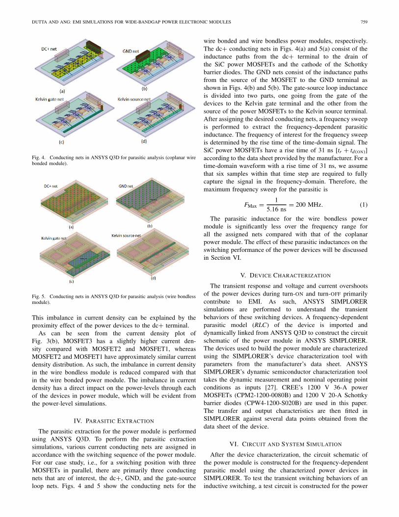
DUTTA AND ANG: EMI SIMULATIONS FOR WIDE-BANDGAP POWER ELECTRONIC MODULES 759
Fig. 4. Conducting nets in ANSYS Q3D for parasitic analysis (coplanar wirebonded module).
Fig. 5. Conducting nets in ANSYS Q3D for parasitic analysis (wire bondlessmodule).
This imbalance in current density can be explained by theproximity effect of the power devices to the dc+ terminal.
As can be seen from the current density plot ofFig. 3(b), MOSFET3 has a slightly higher current den-sity compared with MOSFET2 and MOSFET1, whereasMOSFET2 and MOSFET1 have approximately similar currentdensity distribution. As such, the imbalance in current densityin the wire bondless module is reduced compared with thatin the wire bonded power module. The imbalance in currentdensity has a direct impact on the power-levels through eachof the devices in power module, which will be evident fromthe power-level simulations.
IV. PARASITIC EXTRACTION
The parasitic extraction for the power module is performedusing ANSYS Q3D. To perform the parasitic extractionsimulations, various current conducting nets are assigned inaccordance with the switching sequence of the power module.For our case study, i.e., for a switching position with threeMOSFETs in parallel, there are primarily three conductingnets that are of interest, the dc+, GND, and the gate-sourceloop nets. Figs. 4 and 5 show the conducting nets for the
wire bonded and wire bondless power modules, respectively.The dc+ conducting nets in Figs. 4(a) and 5(a) consist of theinductance paths from the dc+ terminal to the drain ofthe SiC power MOSFETs and the cathode of the Schottkybarrier diodes. The GND nets consist of the inductance pathsfrom the source of the MOSFET to the GND terminal asshown in Figs. 4(b) and 5(b). The gate-source loop inductanceis divided into two parts, one going from the gate of thedevices to the Kelvin gate terminal and the other from thesource of the power MOSFETs to the Kelvin source terminal.After assigning the desired conducting nets, a frequency sweepis performed to extract the frequency-dependent parasiticinductance. The frequency of interest for the frequency sweepis determined by the rise time of the time-domain signal. TheSiC power MOSFETs have a rise time of 31 ns [tr + td (ON)]according to the data sheet provided by the manufacturer. For atime-domain waveform with a rise time of 31 ns, we assumethat six samples within that time step are required to fullycapture the signal in the frequency-domain. Therefore, themaximum frequency sweep for the parasitic is
FMax = 1
5.16 ns= 200 MHz. (1)
The parasitic inductance for the wire bondless powermodule is significantly less over the frequency range forall the assigned nets compared with that of the coplanarpower module. The effect of these parasitic inductances on theswitching performance of the power devices will be discussedin Section VI.
V. DEVICE CHARACTERIZATION
The transient response and voltage and current overshootsof the power devices during turn-ON and turn-OFF primarilycontribute to EMI. As such, ANSYS SIMPLORERsimulations are performed to understand the transientbehaviors of these switching devices. A frequency-dependentparasitic model (RLC) of the device is imported anddynamically linked from ANSYS Q3D to construct the circuitschematic of the power module in ANSYS SIMPLORER.The devices used to build the power module are characterizedusing the SIMPLORER’s device characterization tool withparameters from the manufacturer’s data sheet. ANSYSSIMPLORER’s dynamic semiconductor characterization tooltakes the dynamic measurement and nominal operating pointconditions as inputs [27]. CREE’s 1200 V 36-A powerMOSFETs (CPM2-1200-0080B) and 1200 V 20-A Schottkybarrier diodes (CPW4-1200-S020B) are used in this paper.The transfer and output characteristics are then fitted inSIMPLORER against several data points obtained from thedata sheet of the device.
VI. CIRCUIT AND SYSTEM SIMULATION
After the device characterization, the circuit schematic ofthe power module is constructed for the frequency-dependentparasitic model using the characterized power devices inSIMPLORER. To test the transient switching behaviors of aninductive switching, a test circuit is constructed for the power
760 IEEE JOURNAL OF EMERGING AND SELECTED TOPICS IN POWER ELECTRONICS, VOL. 4, NO. 3, SEPTEMBER 2016
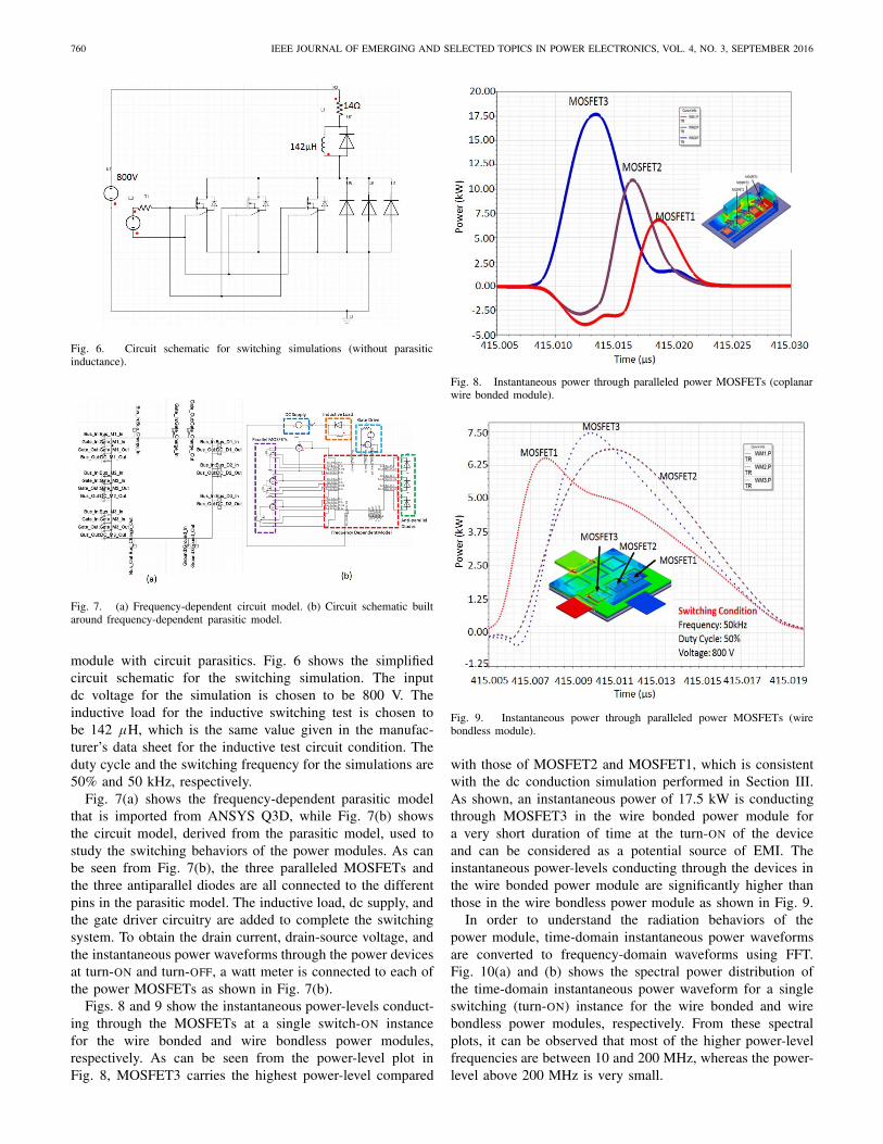
Fig. 6. Circuit schematic for switching simulations (without parasiticinductance).
Fig. 7. (a) Frequency-dependent circuit model. (b) Circuit schematic builtaround frequency-dependent parasitic model.
module with circuit parasitics. Fig. 6 shows the simplifiedcircuit schematic for the switching simulation. The inputdc voltage for the simulation is chosen to be 800 V. Theinductive load for the inductive switching test is chosen tobe 142 μH, which is the same value given in the manufac-turer’s data sheet for the inductive test circuit condition. Theduty cycle and the switching frequency for the simulations are50% and 50 kHz, respectively.
Fig. 7(a) shows the frequency-dependent parasitic modelthat is imported from ANSYS Q3D, while Fig. 7(b) showsthe circuit model, derived from the parasitic model, used tostudy the switching behaviors of the power modules. As canbe seen from Fig. 7(b), the three paralleled MOSFETs andthe three antiparallel diodes are all connected to the differentpins in the parasitic model. The inductive load, dc supply, andthe gate driver circuitry are added to complete the switchingsystem. To obtain the drain current, drain-source voltage, andthe instantaneous power waveforms through the power devicesat turn-ON and turn-OFF, a watt meter is connected to each ofthe power MOSFETs as shown in Fig. 7(b).
Figs. 8 and 9 show the instantaneous power-levels conduct-ing through the MOSFETs at a single switch-ON instancefor the wire bonded and wire bondless power modules,respectively. As can be seen from the power-level plot inFig. 8, MOSFET3 carries the highest power-level compared
Fig. 8. Instantaneous power through paralleled power MOSFETs (coplanarwire bonded module).
Fig. 9. Instantaneous power through paralleled power MOSFETs (wirebondless module).
with those of MOSFET2 and MOSFET1, which is consistentwith the dc conduction simulation performed in Section III.As shown, an instantaneous power of 17.5 kW is conductingthrough MOSFET3 in the wire bonded power module fora very short duration of time at the turn-ON of the deviceand can be considered as a potential source of EMI. Theinstantaneous power-levels conducting through the devices inthe wire bonded power module are significantly higher thanthose in the wire bondless power module as shown in Fig. 9.
In order to understand the radiation behaviors of thepower module, time-domain instantaneous power waveformsare converted to frequency-domain waveforms using FFT.Fig. 10(a) and (b) shows the spectral power distribution ofthe time-domain instantaneous power waveform for a singleswitching (turn-ON) instance for the wire bonded and wirebondless power modules, respectively. From these spectralplots, it can be observed that most of the higher power-levelfrequencies are between 10 and 200 MHz, whereas the power-level above 200 MHz is very small.
DUTTA AND ANG: EMI SIMULATIONS FOR WIDE-BANDGAP POWER ELECTRONIC MODULES 761
Fig. 10. Spectral power-levels through power MOSFETs. (a) Wire bondedmodule. (b) Wire bondless module.
VII. FULL-WAVE SIMULATION
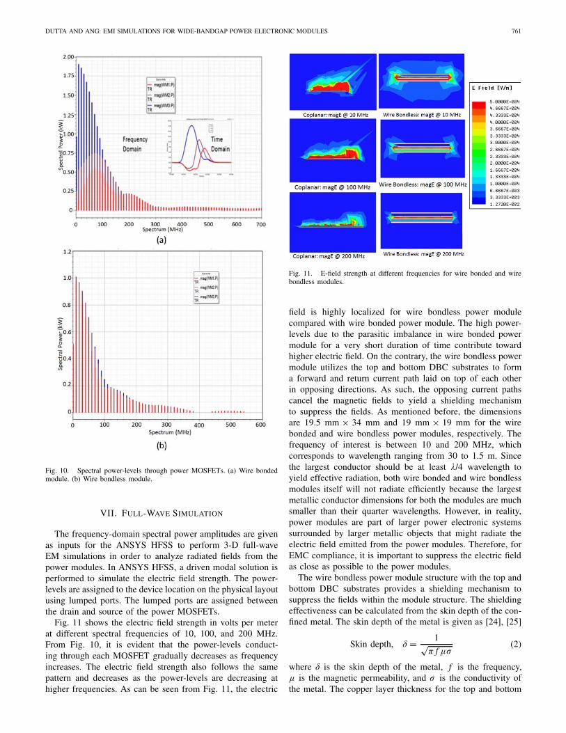
The frequency-domain spectral power amplitudes are givenas inputs for the ANSYS HFSS to perform 3-D full-waveEM simulations in order to analyze radiated fields from thepower modules. In ANSYS HFSS, a driven modal solution isperformed to simulate the electric field strength. The power-levels are assigned to the device location on the physical layoutusing lumped ports. The lumped ports are assigned betweenthe drain and source of the power MOSFETs.
Fig. 11 shows the electric field strength in volts per meterat different spectral frequencies of 10, 100, and 200 MHz.From Fig. 10, it is evident that the power-levels conduct-ing through each MOSFET gradually decreases as frequencyincreases. The electric field strength also follows the samepattern and decreases as the power-levels are decreasing athigher frequencies. As can be seen from Fig. 11, the electric
Fig. 11. E-field strength at different frequencies for wire bonded and wirebondless modules.
field is highly localized for wire bondless power modulecompared with wire bonded power module. The high power-levels due to the parasitic imbalance in wire bonded powermodule for a very short duration of time contribute towardhigher electric field. On the contrary, the wire bondless powermodule utilizes the top and bottom DBC substrates to forma forward and return current path laid on top of each otherin opposing directions. As such, the opposing current pathscancel the magnetic fields to yield a shielding mechanismto suppress the fields. As mentioned before, the dimensionsare 19.5 mm × 34 mm and 19 mm × 19 mm for the wirebonded and wire bondless power modules, respectively. Thefrequency of interest is between 10 and 200 MHz, whichcorresponds to wavelength ranging from 30 to 1.5 m. Sincethe largest conductor should be at least λ/4 wavelength toyield effective radiation, both wire bonded and wire bondlessmodules itself will not radiate efficiently because the largestmetallic conductor dimensions for both the modules are muchsmaller than their quarter wavelengths. However, in reality,power modules are part of larger power electronic systemssurrounded by larger metallic objects that might radiate theelectric field emitted from the power modules. Therefore, forEMC compliance, it is important to suppress the electric fieldas close as possible to the power modules.
The wire bondless power module structure with the top andbottom DBC substrates provides a shielding mechanism tosuppress the fields within the module structure. The shieldingeffectiveness can be calculated from the skin depth of the con-fined metal. The skin depth of the metal is given as [24], [25]
Skin depth, δ = 1√π f μσ
(2)
where δ is the skin depth of the metal, f is the frequency,μ is the magnetic permeability, and σ is the conductivity ofthe metal. The copper layer thickness for the top and bottom
762 IEEE JOURNAL OF EMERGING AND SELECTED TOPICS IN POWER ELECTRONICS, VOL. 4, NO. 3, SEPTEMBER 2016
Fig. 12. Test setup for near-field measurement.
DBC substrates is 304.8-μm. At 10 MHz, the calculated skindepth for copper is approximately 20.3-μm assuming that theconductivity of copper is 5.7 × 10⁷ S/m. The total shieldingeffect can be found by summing the absorption and reflectionlosses given by the following expressions [24], [25]:
Absorption loss, A(dB) = 20loge− tδ (3)
where t is the thickness of the copper layer and δ is the skindepth of copper
Reflection loss, R(dB) = 20 logη0
4ηs(4)
where η0 is the intrinsic free space wave impedance and ηs isthe intrinsic impedance of copper.
The intrinsic impedance of copper is given by [24], [25]
ηs =√
2π f μ
σ. (5)
From the above expressions, the reflection and absorp-tion losses for the 304.8-μm copper are calculated to be98 and 127 dB, respectively. Therefore, the total shieldingeffectiveness for the DBC substrate is 225 dB in any onedirection. As such, wire bondless power modules will providebetter EM compliance compared with wire bonded powermodule.
VIII. RADIATED EMI VALIDATION
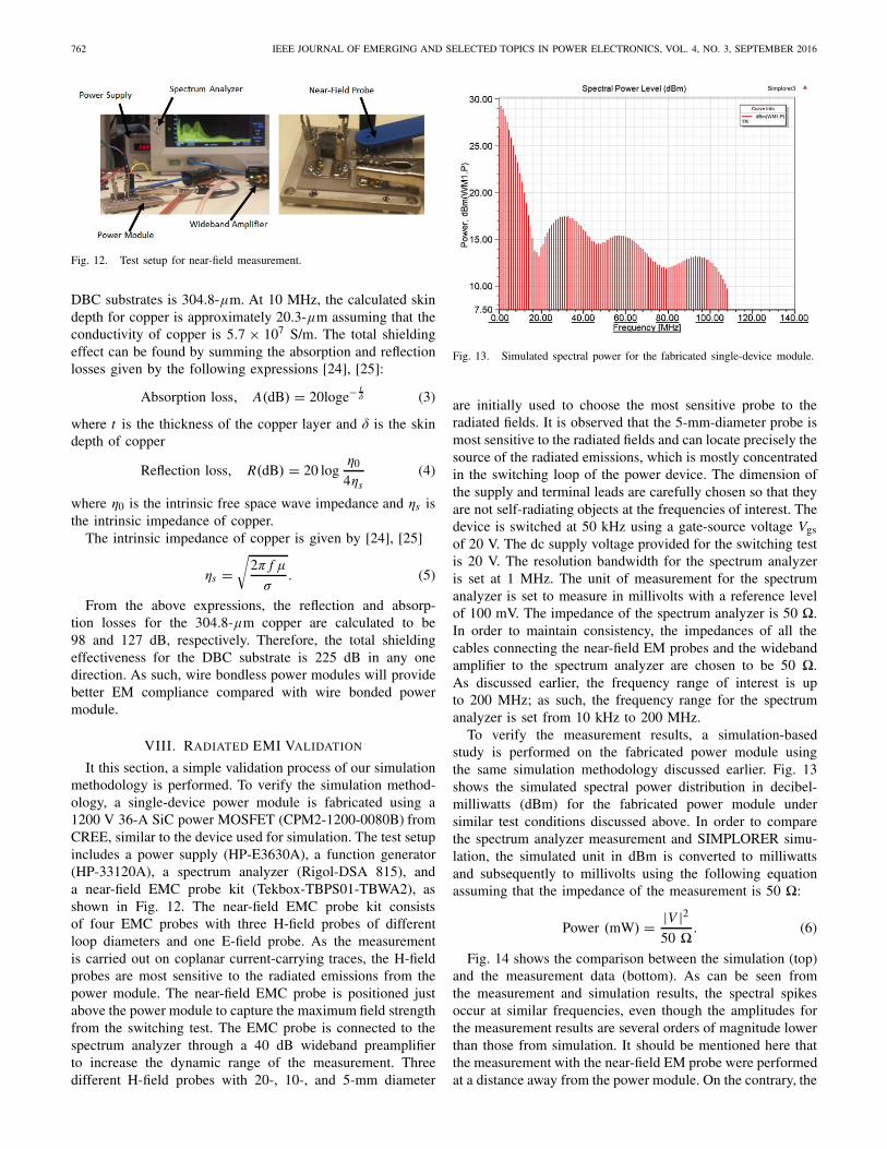
It this section, a simple validation process of our simulationmethodology is performed. To verify the simulation method-ology, a single-device power module is fabricated using a1200 V 36-A SiC power MOSFET (CPM2-1200-0080B) fromCREE, similar to the device used for simulation. The test setupincludes a power supply (HP-E3630A), a function generator(HP-33120A), a spectrum analyzer (Rigol-DSA 815), anda near-field EMC probe kit (Tekbox-TBPS01-TBWA2), asshown in Fig. 12. The near-field EMC probe kit consistsof four EMC probes with three H-field probes of differentloop diameters and one E-field probe. As the measurementis carried out on coplanar current-carrying traces, the H-fieldprobes are most sensitive to the radiated emissions from thepower module. The near-field EMC probe is positioned justabove the power module to capture the maximum field strengthfrom the switching test. The EMC probe is connected to thespectrum analyzer through a 40 dB wideband preamplifierto increase the dynamic range of the measurement. Threedifferent H-field probes with 20-, 10-, and 5-mm diameter
Fig. 13. Simulated spectral power for the fabricated single-device module.
are initially used to choose the most sensitive probe to theradiated fields. It is observed that the 5-mm-diameter probe ismost sensitive to the radiated fields and can locate precisely thesource of the radiated emissions, which is mostly concentratedin the switching loop of the power device. The dimension ofthe supply and terminal leads are carefully chosen so that theyare not self-radiating objects at the frequencies of interest. Thedevice is switched at 50 kHz using a gate-source voltage Vgsof 20 V. The dc supply voltage provided for the switching testis 20 V. The resolution bandwidth for the spectrum analyzeris set at 1 MHz. The unit of measurement for the spectrumanalyzer is set to measure in millivolts with a reference levelof 100 mV. The impedance of the spectrum analyzer is 50 �.In order to maintain consistency, the impedances of all thecables connecting the near-field EM probes and the widebandamplifier to the spectrum analyzer are chosen to be 50 �.As discussed earlier, the frequency range of interest is upto 200 MHz; as such, the frequency range for the spectrumanalyzer is set from 10 kHz to 200 MHz.
To verify the measurement results, a simulation-basedstudy is performed on the fabricated power module usingthe same simulation methodology discussed earlier. Fig. 13shows the simulated spectral power distribution in decibel-milliwatts (dBm) for the fabricated power module undersimilar test conditions discussed above. In order to comparethe spectrum analyzer measurement and SIMPLORER simu-lation, the simulated unit in dBm is converted to milliwattsand subsequently to millivolts using the following equationassuming that the impedance of the measurement is 50 �:
Power (mW) = |V |250 �
. (6)
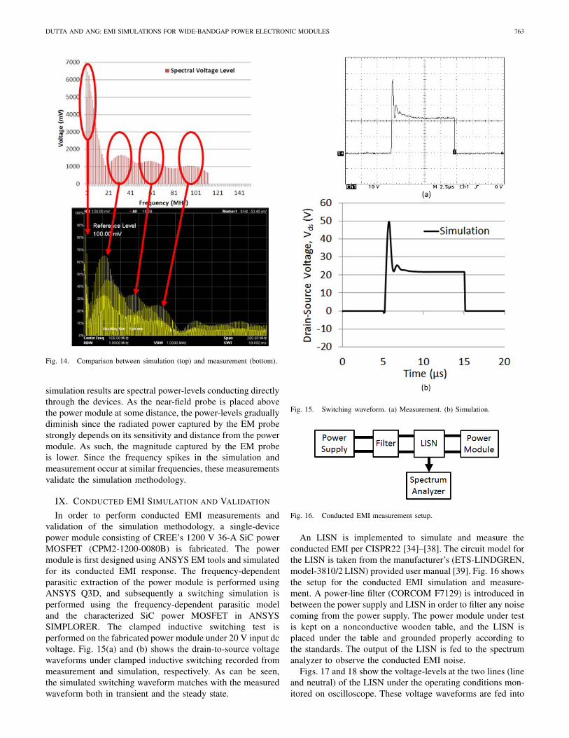
Fig. 14 shows the comparison between the simulation (top)and the measurement data (bottom). As can be seen fromthe measurement and simulation results, the spectral spikesoccur at similar frequencies, even though the amplitudes forthe measurement results are several orders of magnitude lowerthan those from simulation. It should be mentioned here thatthe measurement with the near-field EM probe were performedat a distance away from the power module. On the contrary, the
DUTTA AND ANG: EMI SIMULATIONS FOR WIDE-BANDGAP POWER ELECTRONIC MODULES 763
Fig. 14. Comparison between simulation (top) and measurement (bottom).
simulation results are spectral power-levels conducting directlythrough the devices. As the near-field probe is placed abovethe power module at some distance, the power-levels graduallydiminish since the radiated power captured by the EM probestrongly depends on its sensitivity and distance from the powermodule. As such, the magnitude captured by the EM probeis lower. Since the frequency spikes in the simulation andmeasurement occur at similar frequencies, these measurementsvalidate the simulation methodology.
IX. CONDUCTED EMI SIMULATION AND VALIDATION
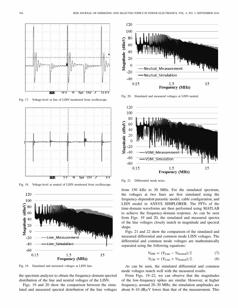
In order to perform conducted EMI measurements andvalidation of the simulation methodology, a single-devicepower module consisting of CREE’s 1200 V 36-A SiC powerMOSFET (CPM2-1200-0080B) is fabricated. The powermodule is first designed using ANSYS EM tools and simulatedfor its conducted EMI response. The frequency-dependentparasitic extraction of the power module is performed usingANSYS Q3D, and subsequently a switching simulation isperformed using the frequency-dependent parasitic modeland the characterized SiC power MOSFET in ANSYSSIMPLORER. The clamped inductive switching test isperformed on the fabricated power module under 20 V input dcvoltage. Fig. 15(a) and (b) shows the drain-to-source voltagewaveforms under clamped inductive switching recorded frommeasurement and simulation, respectively. As can be seen,the simulated switching waveform matches with the measuredwaveform both in transient and the steady state.
Fig. 15. Switching waveform. (a) Measurement. (b) Simulation.
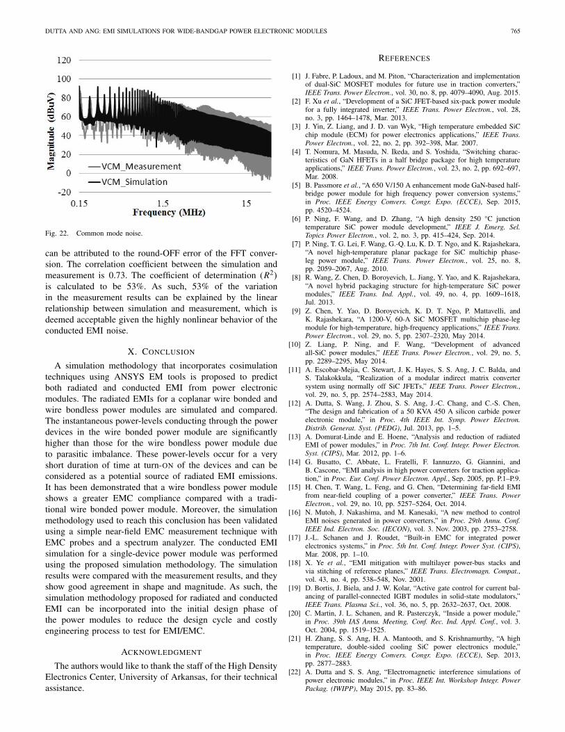
Fig. 16. Conducted EMI measurement setup.
An LISN is implemented to simulate and measure theconducted EMI per CISPR22 [34]–[38]. The circuit model forthe LISN is taken from the manufacturer’s (ETS-LINDGREN,model-3810/2 LISN) provided user manual [39]. Fig. 16 showsthe setup for the conducted EMI simulation and measure-ment. A power-line filter (CORCOM F7129) is introduced inbetween the power supply and LISN in order to filter any noisecoming from the power supply. The power module under testis kept on a nonconductive wooden table, and the LISN isplaced under the table and grounded properly according tothe standards. The output of the LISN is fed to the spectrumanalyzer to observe the conducted EMI noise.
Figs. 17 and 18 show the voltage-levels at the two lines (lineand neutral) of the LISN under the operating conditions mon-itored on oscilloscope. These voltage waveforms are fed into
764 IEEE JOURNAL OF EMERGING AND SELECTED TOPICS IN POWER ELECTRONICS, VOL. 4, NO. 3, SEPTEMBER 2016
Fig. 17. Voltage-level at line of LISN monitored from oscilloscope.
Fig. 18. Voltage-level at neutral of LISN monitored from oscilloscope.
Fig. 19. Simulated and measured voltages at LISN line.
the spectrum analyzer to obtain the frequency-domain spectraldistribution of the line and neutral voltages of the LISN.
Figs. 19 and 20 show the comparison between the simu-lated and measured spectral distribution of the line voltages
Fig. 20. Simulated and measured voltages at LISN neutral.
Fig. 21. Differential mode noise.
from 150 kHz to 30 MHz. For the simulated spectrum,the voltages at two lines are first simulated using thefrequency-dependent parasitic model, cable configuration, andLISN model in ANSYS SIMPLORER. The FFTs of thetime-domain waveforms are then performed using MATLABto achieve the frequency-domain response. As can be seenfrom Figs. 19 and 20, the simulated and measured spectraof the line voltages closely match in magnitude and spectralshape.
Figs. 21 and 22 show the comparison of the simulated andmeasured differential and common mode LISN voltages. Thedifferential and common mode voltages are mathematicallyseparated using the following equations:
VDM = (VLine − VNeutral)/2 (7)
VCM = (VLine + VNeutral)/2. (8)
As can be seen, the simulated differential and commonmode voltages match well with the measured results.
From Figs. 19–22, we can observe that the magnitudesof the low-frequency spikes are similar. However, at higherfrequency, around 20–30 MHz, the simulation amplitudes areabout 8–10 dBμV lower than that of the measurement. This
DUTTA AND ANG: EMI SIMULATIONS FOR WIDE-BANDGAP POWER ELECTRONIC MODULES 765
Fig. 22. Common mode noise.
can be attributed to the round-OFF error of the FFT conver-sion. The correlation coefficient between the simulation andmeasurement is 0.73. The coefficient of determination (R2)is calculated to be 53%. As such, 53% of the variationin the measurement results can be explained by the linearrelationship between simulation and measurement, which isdeemed acceptable given the highly nonlinear behavior of theconducted EMI noise.
X. CONCLUSION
A simulation methodology that incorporates cosimulationtechniques using ANSYS EM tools is proposed to predictboth radiated and conducted EMI from power electronicmodules. The radiated EMIs for a coplanar wire bonded andwire bondless power modules are simulated and compared.The instantaneous power-levels conducting through the powerdevices in the wire bonded power module are significantlyhigher than those for the wire bondless power module dueto parasitic imbalance. These power-levels occur for a veryshort duration of time at turn-ON of the devices and can beconsidered as a potential source of radiated EMI emissions.It has been demonstrated that a wire bondless power moduleshows a greater EMC compliance compared with a tradi-tional wire bonded power module. Moreover, the simulationmethodology used to reach this conclusion has been validatedusing a simple near-field EMC measurement technique withEMC probes and a spectrum analyzer. The conducted EMIsimulation for a single-device power module was performedusing the proposed simulation methodology. The simulationresults were compared with the measurement results, and theyshow good agreement in shape and magnitude. As such, thesimulation methodology proposed for radiated and conductedEMI can be incorporated into the initial design phase ofthe power modules to reduce the design cycle and costlyengineering process to test for EMI/EMC.
ACKNOWLEDGMENT
The authors would like to thank the staff of the High DensityElectronics Center, University of Arkansas, for their technicalassistance.
REFERENCES
[1] J. Fabre, P. Ladoux, and M. Piton, “Characterization and implementationof dual-SiC MOSFET modules for future use in traction converters,”IEEE Trans. Power Electron., vol. 30, no. 8, pp. 4079–4090, Aug. 2015.
[2] F. Xu et al., “Development of a SiC JFET-based six-pack power modulefor a fully integrated inverter,” IEEE Trans. Power Electron., vol. 28,no. 3, pp. 1464–1478, Mar. 2013.
[3] J. Yin, Z. Liang, and J. D. van Wyk, “High temperature embedded SiCchip module (ECM) for power electronics applications,” IEEE Trans.Power Electron., vol. 22, no. 2, pp. 392–398, Mar. 2007.
[4] T. Nomura, M. Masuda, N. Ikeda, and S. Yoshida, “Switching charac-teristics of GaN HFETs in a half bridge package for high temperatureapplications,” IEEE Trans. Power Electron., vol. 23, no. 2, pp. 692–697,Mar. 2008.
[5] B. Passmore et al., “A 650 V/150 A enhancement mode GaN-based half-bridge power module for high frequency power conversion systems,”in Proc. IEEE Energy Convers. Congr. Expo. (ECCE), Sep. 2015,pp. 4520–4524.
[6] P. Ning, F. Wang, and D. Zhang, “A high density 250 °C junctiontemperature SiC power module development,” IEEE J. Emerg. Sel.Topics Power Electron., vol. 2, no. 3, pp. 415–424, Sep. 2014.
[7] P. Ning, T. G. Lei, F. Wang, G.-Q. Lu, K. D. T. Ngo, and K. Rajashekara,“A novel high-temperature planar package for SiC multichip phase-leg power module,” IEEE Trans. Power Electron., vol. 25, no. 8,pp. 2059–2067, Aug. 2010.
[8] R. Wang, Z. Chen, D. Boroyevich, L. Jiang, Y. Yao, and K. Rajashekara,“A novel hybrid packaging structure for high-temperature SiC powermodules,” IEEE Trans. Ind. Appl., vol. 49, no. 4, pp. 1609–1618,Jul. 2013.
[9] Z. Chen, Y. Yao, D. Boroyevich, K. D. T. Ngo, P. Mattavelli, andK. Rajashekara, “A 1200-V, 60-A SiC MOSFET multichip phase-legmodule for high-temperature, high-frequency applications,” IEEE Trans.Power Electron., vol. 29, no. 5, pp. 2307–2320, May 2014.
[10] Z. Liang, P. Ning, and F. Wang, “Development of advancedall-SiC power modules,” IEEE Trans. Power Electron., vol. 29, no. 5,pp. 2289–2295, May 2014.
[11] A. Escobar-Mejia, C. Stewart, J. K. Hayes, S. S. Ang, J. C. Balda, andS. Talakokkula, “Realization of a modular indirect matrix convertersystem using normally off SiC JFETs,” IEEE Trans. Power Electron.,vol. 29, no. 5, pp. 2574–2583, May 2014.
[12] A. Dutta, S. Wang, J. Zhou, S. S. Ang, J.-C. Chang, and C.-S. Chen,“The design and fabrication of a 50 KVA 450 A silicon carbide powerelectronic module,” in Proc. 4th IEEE Int. Symp. Power Electron.Distrib. Generat. Syst. (PEDG), Jul. 2013, pp. 1–5.
[13] A. Domurat-Linde and E. Hoene, “Analysis and reduction of radiatedEMI of power modules,” in Proc. 7th Int. Conf. Integr. Power Electron.Syst. (CIPS), Mar. 2012, pp. 1–6.
[14] G. Busatto, C. Abbate, L. Fratelli, F. Iannuzzo, G. Giannini, andB. Cascone, “EMI analysis in high power converters for traction applica-tion,” in Proc. Eur. Conf. Power Electron. Appl., Sep. 2005, pp. P.1–P.9.
[15] H. Chen, T. Wang, L. Feng, and G. Chen, “Determining far-field EMIfrom near-field coupling of a power converter,” IEEE Trans. PowerElectron., vol. 29, no. 10, pp. 5257–5264, Oct. 2014.
[16] N. Mutoh, J. Nakashima, and M. Kanesaki, “A new method to controlEMI noises generated in power converters,” in Proc. 29th Annu. Conf.IEEE Ind. Electron. Soc. (IECON), vol. 3. Nov. 2003, pp. 2753–2758.
[17] J.-L. Schanen and J. Roudet, “Built-in EMC for integrated powerelectronics systems,” in Proc. 5th Int. Conf. Integr. Power Syst. (CIPS),Mar. 2008, pp. 1–10.
[18] X. Ye et al., “EMI mitigation with multilayer power-bus stacks andvia stitching of reference planes,” IEEE Trans. Electromagn. Compat.,vol. 43, no. 4, pp. 538–548, Nov. 2001.
[19] D. Bortis, J. Biela, and J. W. Kolar, “Active gate control for current bal-ancing of parallel-connected IGBT modules in solid-state modulators,”IEEE Trans. Plasma Sci., vol. 36, no. 5, pp. 2632–2637, Oct. 2008.
[20] C. Martin, J. L. Schanen, and R. Pasterczyk, “Inside a power module,”in Proc. 39th IAS Annu. Meeting, Conf. Rec. Ind. Appl. Conf., vol. 3.Oct. 2004, pp. 1519–1525.
[21] H. Zhang, S. S. Ang, H. A. Mantooth, and S. Krishnamurthy, “A hightemperature, double-sided cooling SiC power electronics module,”in Proc. IEEE Energy Convers. Congr. Expo. (ECCE), Sep. 2013,pp. 2877–2883.
[22] A. Dutta and S. S. Ang, “Electromagnetic interference simulations ofpower electronic modules,” in Proc. IEEE Int. Workshop Integr. PowerPackag. (IWIPP), May 2015, pp. 83–86.
766 IEEE JOURNAL OF EMERGING AND SELECTED TOPICS IN POWER ELECTRONICS, VOL. 4, NO. 3, SEPTEMBER 2016
[23] E. Hoene, A. Ostmann, and C. Marczok, “Packaging very fast switchingsemiconductors,” in Proc. 8th Int. Conf. Integr. Power Syst. (CIPS),Feb. 2014, pp. 1–7.
[24] H. W. Ott, Electromagnetic Compatibility Engineering. Hoboken, NJ,USA: Wiley, 2009.
[25] C. R. Paul, Introduction to Electromagnetic Compatibility. Hoboken, NJ,USA: Wiley, 2006.
[26] User’s Guide-Maxwell 3D, ANSYS Inc., Canonsburg, PA, USA, 2012.[27] SIMPLORER Online Help, ANSYS Inc., Canonsburg, PA, USA, 2015.[28] ANSYS Electronic Desktop Online Help, ANSYS Inc., Canonsburg, PA,
USA, 2015.[29] G. Antonini, S. Cristina, and A. Orlandi, “EMC characterization of
SMPS devices: Circuit and radiated emissions model,” IEEE Trans.Electromagn. Compat., vol. 38, no. 3, pp. 300–309, Aug. 1996.
[30] O. Aouine, C. Labarre, and F. Costa, “Measurement and modelingof the magnetic near field radiated by a buck chopper,” IEEE Trans.Electromagn. Compat., vol. 50, no. 2, pp. 445–449, May 2008.
[31] E. Gubia, P. Sanchis, A. Ursua, J. Lopez, and L. Marroyo, “Frequencydomain model of conducted EMI in electrical drives,” IEEE PowerElectron. Lett., vol. 3, no. 2, pp. 45–49, Jun. 2005.
[32] H. Zhu, J.-S. Lai, A. R. Hefner, Y. Tang, and C. Chen, “Modeling-basedexamination of conducted EMI emissions from hard and soft-switchingPWM inverters,” IEEE Trans. Ind. Appl., vol. 37, no. 5, pp. 1383–1393,Sep./Oct. 2001.
[33] J.-S. Lai, X. Huang, E. Pepa, S. Chen, and T. W. Nehl, “Inverter EMImodeling and simulation methodologies,” IEEE Trans. Ind. Electron.,vol. 53, no. 3, pp. 736–744, Jun. 2006.
[34] American National Standard for Limits and Methods of Mea-surement of Radio Disturbance Characteristics of InformationTechnology Equipment, ANSI Standard C63.022-1 996, 1997,doi: 10.1109/IEEESTD.1997.85256.
[35] F. Giezendanner, J. Biela, J. W. Kolar, and S. Zudrell-Koch, “EMI noiseprediction for electronic ballasts,” IEEE Trans. Power Electron., vol. 25,no. 8, pp. 2133–2141, Aug. 2010.
[36] M. Kumar and V. Agarwal, “Power line filter design for conductedelectromagnetic interference using time-domain measurements,” IEEETrans. Electromagn. Compat., vol. 48, no. 1, pp. 178–186, Feb. 2006.
[37] M. R. Yazdani, H. Farzanehfard, and J. Faiz, “EMI analysis andevaluation of an improved ZCT flyback converter,” IEEE Trans. PowerElectron., vol. 26, no. 8, pp. 2326–2334, Aug. 2011.
[38] S. Wang, F. C. Lee, and W. G. Odendaal, “Characterization, evaluation,and design of noise separator for conducted EMI noise diagnosis,” IEEETrans. Power Electron., vol. 20, no. 4, pp. 974–982, Jul. 2005.
[39] User Manual, Line Impedance Stabilization Network (LISN), ETS-LINDGREN, An ESCO Technol. Company, Cedar Park, TX, USA,1996.
Atanu Dutta (S’14) was born in Dhaka,Bangladesh, in 1984. He received the B.Tech. degreein electronic and communication engineering fromthe National Institute of Technology, Durgapur,India, in 2007, and the M.S. degree in electricalengineering from the University of Arkansas,Fayetteville, AR, USA, in 2010, where he iscurrently pursuing the Ph.D. degree in electricalengineering.
His current research interests include high powerelectronic packaging, structural development of
high power electronic module, electromagnetic interference/electromagneticcompatibility in power converters, and process engineering.
Simon S. Ang (S’79–M’79–SM’94–F’11) receivedthe B.S.E.E. degree from the University of Arkansas,Fayetteville, AR, USA, the M.S.E.E. degree from theGeorgia Institute of Technology, Atlanta, GA, USA,and the Ph.D. degree in electrical engineering fromSouthern Methodist University, Dallas, TX, USA.
He is currently a Professor of Electrical Engineer-ing and the Director of the High Density ElectronicsCenter with the University of Arkansas. He hasauthored or co-authored over 290 journal and pro-ceeding articles. He has authored the book entitled
Power-Switching Converters—Third Edition (New York: CRC Press, 2010).Dr. Ang is a fellow of the Institution of Engineering and Technology in
the U.K., the Electrochemical Society, and the City and Guilds of LondonInstitute in the U.K.