Embed Size (px)
Citation preview
IEEE JOURNAL OF SOLID-STATE CIRCUITS, VOL. 45, NO. 4, APRIL 2010 843
An Efficient 10GBASE-T Ethernet LDPC DecoderDesign With Low Error Floors
Zhengya Zhang, Member, IEEE, Venkat Anantharam, Fellow, IEEE, Martin J. Wainwright, Member, IEEE, andBorivoje Nikolic, Senior Member, IEEE
Abstract—A grouped-parallel low-density parity-check (LDPC)decoder is designed for the (2048,1723) Reed-Solomon-basedLDPC (RS-LDPC) code suitable for 10GBASE-T Ethernet. Atwo-step decoding scheme reduces the wordlength to 4 bits whilelowering the error floor to below 10 �� BER. The proposedpost-processor is conveniently integrated with the decoder, addingminimal area and power. The decoder architecture is optimized bygroupings so as to localize irregular interconnects and regularizeglobal interconnects and the overall wiring overhead is minimized.The 5.35 mm�, 65 nm CMOS chip achieves a decoding throughputof 47.7 Gb/s. With scaled frequency and voltage, the chip delivers a6.67 Gb/s throughput necessary for 10GBASE-T while dissipating144 mW of power.
Index Terms—Error floors, iterative decoder architecture,low-density parity-check (LDPC) code, message-passing decoding,post-processing.
I. INTRODUCTION
L OW-DENSITY parity-check (LDPC) codes have beendemonstrated to perform very close to the Shannon
limit when decoded iteratively using message-passing algo-rithms [1]–[4]. A wide array of the latest communication andstorage systems have chosen LDPC codes for forward errorcorrection in applications including digital video broadcasting(DVB-S2) [5], [6], 10 Gigabit Ethernet (10GBASE-T) [7],broadband wireless access (WiMax) [8], wireless local areanetwork (WiFi) [9], deep-space communications [10], andmagnetic storage in hard disk drives [11]. The adoption of thecapacity-approaching LDPC codes is, at least in theory, oneof the keys to achieving lower transmission power and morereliable communication.
Manuscript received August 24, 2009; revised January 15, 2010. Current ver-sion published March 24, 2010. This paper was approved by Guest Editor AjithAmerasekera. This work was supported in part by NSF CCF Grant 0635372,Marvell Semiconductor, and Intel Corporation through a UC MICRO Grant.The design infrastructure was developed with the support of Center for Circuitand System Solutions (C2S2) Focus Center, one of five research centers fundedunder the Focus Center Research Program, a Semiconductor Research Corpo-ration program. The NSF Grant CNS RI-0403427 provided the computing in-frastructure and ST Microelectronics donated the chip fabrication.
Z. Zhang was with the Department of Electrical Engineering and ComputerSciences, University of California, Berkeley, and is now with the Departmentof Electrical Engineering and Computer Science, University of Michigan, AnnArbor, MI 48109 USA (e-mail: [email protected]).
V. Anantharam, M. J. Wainwright, and B. Nikolic are with the De-partment of Electrical Engineering and Computer Sciences, University ofCalifornia, Berkeley, CA 94720 USA (e-mail: [email protected];[email protected]; [email protected]).
Color versions of one or more of the figures in this paper are available onlineat http://ieeexplore.ieee.org.
Digital Object Identifier 10.1109/JSSC.2010.2042255
There is a challenge in implementing high-throughput LDPCdecoders with a low area and power on a silicon chip for prac-tical applications. The intrinsically parallel message-passing de-coding algorithm relies on message exchange between variableprocessing nodes (VN) and check processing nodes (CN) in thegraph defined by the matrix. A direct mapping of the inter-connection graph causes large wiring overhead and low area uti-lization. In the first silicon implementation of a fully parallel de-coder, Blanksby and Howland reported that the size of the de-coder was determined by routing congestion and not by the gatecount [12]. Even with optimized floor plan and buffer placementtechniques, the area utilization rate is only 50%.
Architectures with lower parallelism can be attractive, as thearea efficiency can be improved. In the decoder used in an ultra-wideband (UWB) baseband transceiver [13], the matrix ispartitioned: partitions are time-multiplexed and each partition isprocessed in a fully parallel manner. With structured codes, therouting can be further simplified. Examples include the decodersfor the DVB-S2 standard [14], [15], where the connection be-tween memory and processors is realized using barrel shifters. Amore compact routing scheme, only for codes constructed withcirculant matrices, is to fix the wiring between memory andprocessors while rotating data stored in shift registers [16]. Themore generic and most common grouped-parallel architectureis implemented in segmented memories to increase the accessbandwidth and the schedules are controlled by lookup tables.Architectures constructed this way permit reconfigurability, asdemonstrated by a WiMAX decoder [17].
Solely relying on architecture transformation could be lim-iting in producing the optimal designs. Novel schemes havebeen proposed for achieving the design specification with noaddition (or even a reduction) of the architectural overhead. Inthe work [18], a layered decoding schedule was implementedby interleaving check and variable node operations in order tospeed up convergence and increase throughput. This scheme re-quires additional processing and a higher power consumption.Other authors [19] have used a bit-serial arithmetic to reducethe number of interconnects by a factor equal to the wordlength,thereby lowering the wiring overhead in a fully parallel archi-tecture. This bit-serial architecture was demonstrated for a smallLDPC code with a block length of 660. More complex codescan still be difficult to implement due to the poor scalability ofglobal wires.
Aside from the implementation challenges, LDPC codesare not guaranteed to perform well in every application either.Sometimes the excellent error-correction performance ofLDPC codes is only observed up until a moderate bit error rate
0018-9200/$26.00 © 2010 IEEE
Authorized licensed use limited to: UC BERKELEY CDL. Downloaded on May 21,2010 at 01:26:11 UTC from IEEE Xplore. Restrictions apply.
844 IEEE JOURNAL OF SOLID-STATE CIRCUITS, VOL. 45, NO. 4, APRIL 2010
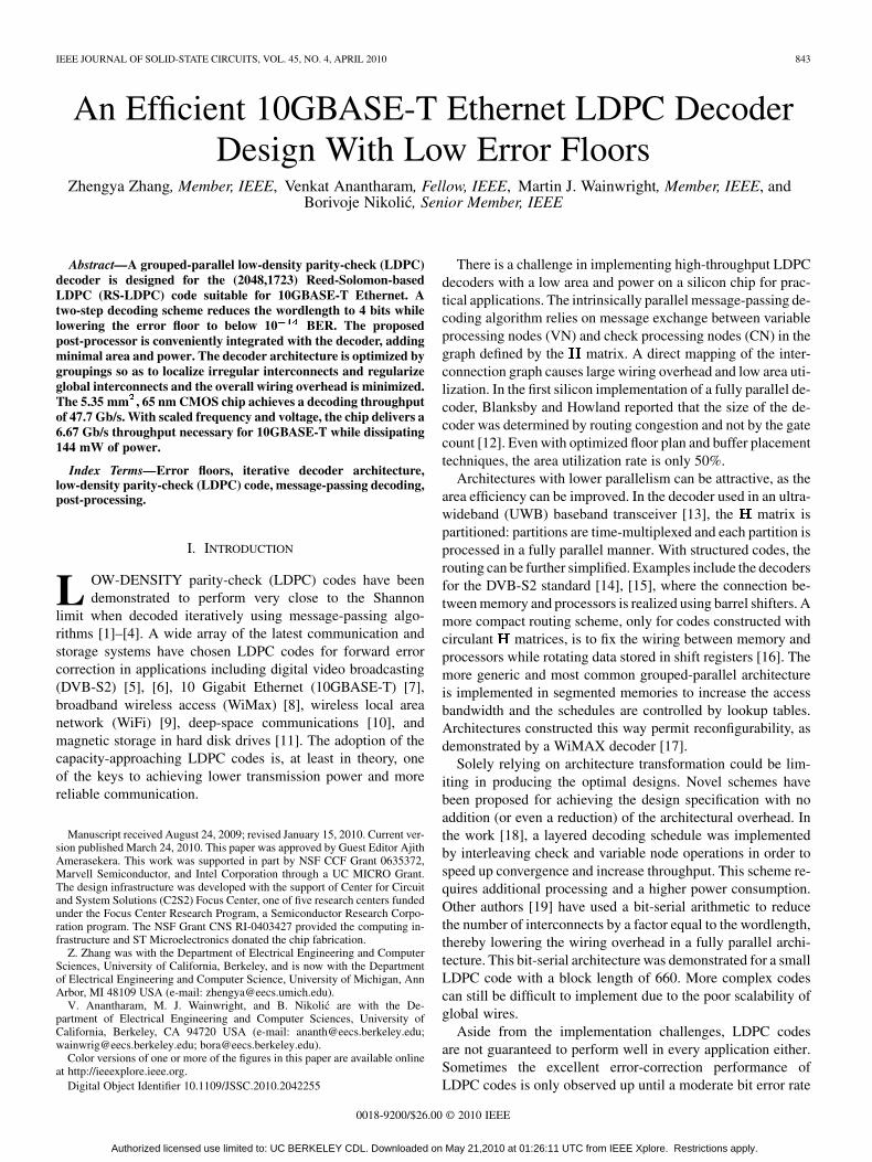
Fig. 1. Representation of an LDPC code in (a) a parity-check matrix (� matrix) and (b) a factor graph.
(BER); at a lower BER, the error curve often changes its slope,manifesting a so-called error floor [20]. With communicationand storage systems demanding data rates up to Gb/s, relativelyhigh error floors degrade the quality of service. To prevent suchdegradation, transmission power is raised or a more complexscheme, such as an additional level of error-correction coding[5], is created. These approaches increase the power consump-tion and complicate the system integration.
This work implements a post-processing algorithm that uti-lizes aspects of the structure of the Tanner graph associatedto the LDPC code [21], [22]. The post-processing approach isbased on a message-passing algorithm with selectively-biasedmessages. As a result, it can be seamlessly integrated with themessage-passing decoder. Results show performance improve-ment of orders of magnitude at low error rates after post-pro-cessing even with short wordlengths. The wordlength reductionpermits a more compact physical implementation.
In formulating the hardware architecture of a high-throughputdecoder, a grouping strategy is applied in separating irregularlocal wires from regular global wires. The post-processor is im-plemented as a small add-on to each local processing elementwithout adding external wiring, thus the area penalty is keptminimal. A low wiring overhead enables a highly parallel de-coder design that achieves a very high throughput. Frequencyand voltage scaling can be applied to improve power efficiencyif a lower throughput is desired.
In this paper, Section II introduces the LDPC code and thedecoding algorithm. Emphasis is placed on LDPC codes con-structed in a structured way and its implication on the decoderarchitecture. In Section III, hardware emulation is applied inchoosing the decoding algorithm and wordlength. In particular,the post-processing algorithm is demonstrated to achieve anexcellent decoding performance at a very short wordlength of4 bits. In Section IV, the architecture of the chip is determinedbased on a set of experiments to explore how architecturalgrouping affects implementation results. Section V explainsindividual block designs and Section VI presents steps inoptimizing the overall area and power efficiencies. The perfor-mance and power measurements of the fabricated test chip arepresented in Section VII.
II. BACKGROUND
A low-density parity-check code is a linear block code, de-fined by a sparse parity check matrix where rep-
resents the number of bits in the code block (block length) andrepresents the number of parity checks. An example of the
matrix of an LDPC code is shown in Fig. 1(a). The matrix canbe represented graphically using a factor graph as in Fig. 1(b),where each bit is represented by a variable node and each checkis represented by a factor (check) node. An edge exists betweenthe variable node and the check node if .
A. Decoding Algorithm
Low-density parity-check codes are usually iteratively de-coded using the belief propagation algorithm, also known asthe message-passing algorithm. The message-passing algorithmoperates on a factor graph, where soft messages are exchangedbetween variable nodes and check nodes. The algorithm can beformulated as follows: in the first step, variable nodes are ini-tialized with the prior log-likelihood ratios (LLR) defined in (1)using the channel outputs , where represents the channelnoise variance. This formulation assumes the information bitstake on the values 0 and 1 with equal probability.
(1)
The variable nodes send messages to the check nodes alongthe edges defined by the factor graph. The LLRs are recom-puted based on the parity constraints at each check node andreturned to the neighboring variable nodes. Each variable nodethen updates its decision based on the channel output and theextrinsic information received from all the neighboring checknodes. The marginalized posterior information is used as thevariable-to-check message in the next iteration.
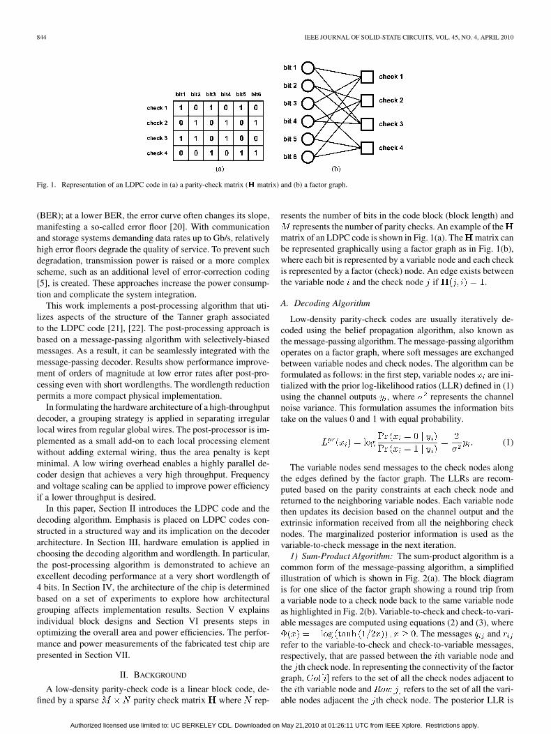
1) Sum-Product Algorithm: The sum-product algorithm is acommon form of the message-passing algorithm, a simplifiedillustration of which is shown in Fig. 2(a). The block diagramis for one slice of the factor graph showing a round trip froma variable node to a check node back to the same variable nodeas highlighted in Fig. 2(b). Variable-to-check and check-to-vari-able messages are computed using equations (2) and (3), where
. The messages andrefer to the variable-to-check and check-to-variable messages,respectively, that are passed between the th variable node andthe th check node. In representing the connectivity of the factorgraph, refers to the set of all the check nodes adjacent tothe th variable node and refers to the set of all the vari-able nodes adjacent the th check node. The posterior LLR is
Authorized licensed use limited to: UC BERKELEY CDL. Downloaded on May 21,2010 at 01:26:11 UTC from IEEE Xplore. Restrictions apply.
ZHANG et al.: AN EFFICIENT 10GBASE-T ETHERNET LDPC DECODER DESIGN WITH LOW ERROR FLOORS 845
Fig. 2. Message-passing decoding implementation showing (a) sum-product message-passing decoding, (b) the corresponding one slice of a factor graph, and(c) min-sum message-passing decoding.
computed in each iteration using the update (4). A hard deci-sion is made based on the posterior LLR in every iteration. Theiterative decoding algorithm is allowed to run until the hard de-cisions satisfy all the parity check equations or when an upperlimit on the iteration number is reached, whichever occurs ear-lier.
(2)
(3)
(4)
2) Min-Sum Approximation: Equation (3) can be simplifiedby observing that the magnitude of is usually dominatedby the minimum term, and thus this minimum termcan be used as an approximation of the magnitude of , as
shown in the papers [23], [24]. The magnitude of com-puted using such min-sum approximation is usually overesti-mated and correction terms are introduced to reduce the approx-imation error. The correction can be in the form of an offset [25],shown as in the update (5).
(5)
3) Reordered Schedule: The above equations can also be re-arranged by taking into account the relationship between con-secutive decoding iterations. A variable-to-check message ofiteration can be computed by subtracting the correspondingcheck-to-variable message from the posterior LLR of iteration
as in (6), while the posterior LLR of iteration can becomputed by updating the posterior LLR of the previous itera-tion with the check-to-variable message of iteration , as in (7).
(6)
(7)
Authorized licensed use limited to: UC BERKELEY CDL. Downloaded on May 21,2010 at 01:26:11 UTC from IEEE Xplore. Restrictions apply.
846 IEEE JOURNAL OF SOLID-STATE CIRCUITS, VOL. 45, NO. 4, APRIL 2010
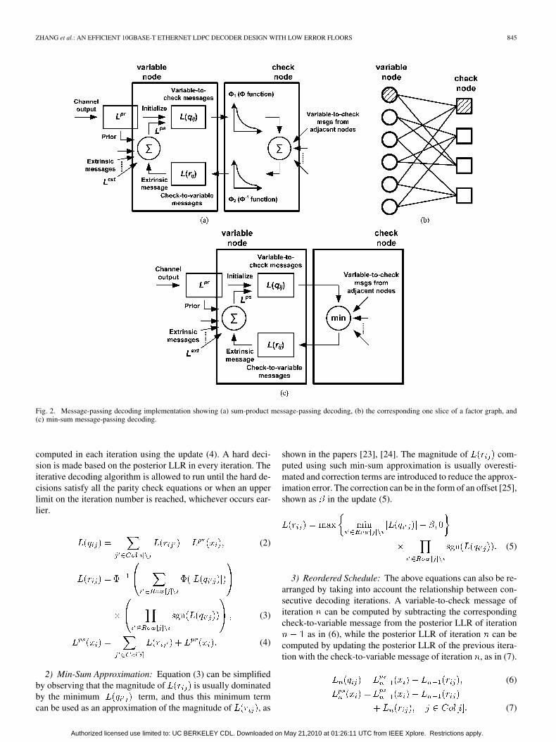
Fig. 3. Illustration of the subgraph induced by the incorrect bits in an (8,8) fully absorbing set.
B. Structured LDPC Codes
A practical high-throughput LDPC decoder can be imple-mented in a fully parallel manner by directly mapping the factorgraph onto an array of processing elements interconnected bywires. Each variable node is mapped to a variable processingnode (VN) and each check node is mapped to a check processingnode (CN), such that all messages from variable nodes to checknodes and then in reverse are processed concurrently. Practicalhigh-performance LDPC codes commonly feature block lengthson the order of 1kb and up to 64kb, requiring a large number ofVNs. The ensuing wiring overhead poses a substantial obstacletowards efficient silicon implementations.
Structured LDPC codes of moderate block lengths have re-ceived more attention in practice recently because they proveamenable for efficient decoder architectures and recent pub-lished standards have adopted such LDPC codes [7]–[9]. The
matrices of these structured LDPC codes consist of compo-nent matrices, each of which is, or closely resembles, a permu-tation matrix or a zero matrix. Structured codes open the doorto a range of efficient high-throughput decoder architectures bytaking advantage of the regularity in wiring and data storage.In this work, a highly parallel LDPC decoder design is demon-strated for a (6,32)-regular (2048,1723) RS-LDPC code [26].This particular LDPC code has been adopted for the forwarderror correction in the IEEE 802.3an 10GBASE-T standard [7],which governs the operation of 10 Gigabit Ethernet over up to100 m of CAT-6a unshielded twisted-pair (UTP) cable. Thematrix of this code contains 384 rows and 2048columns. This matrix can be partitioned into 6 row groups and32 column groups of 64 64 permutation submatrices.
III. EMULATION-BASED STUDY
An FPGA-based hardware emulation has been used to ini-tially investigate the low error rate performance of this code, andit has been discovered that a class of (8,8) absorbing-set errorsdominate the error floors [22], [27]. A subgraph illustrating the(8,8) absorbing set is shown in Fig. 3, representing a substruc-ture of the factor graph associated with the LDPC code. Con-sider a state with all eight variable nodes of an (8,8) absorbingset in error—a state that cannot be decoded successfully by amessage-passing decoder because the variable nodes that con-stitute the absorbing set reinforce the incorrect values amongthemselves through the cycles in the graph. More precisely, eachvariable node receives one message from a unsatisfied check
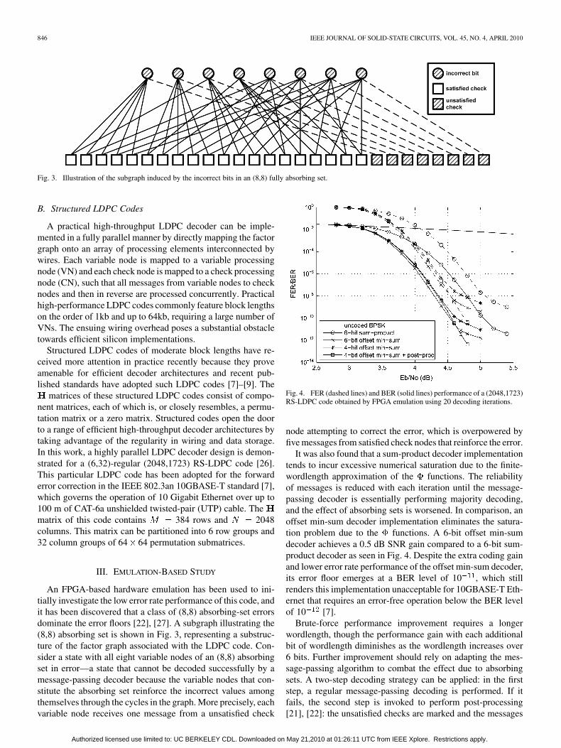
Fig. 4. FER (dashed lines) and BER (solid lines) performance of a (2048,1723)RS-LDPC code obtained by FPGA emulation using 20 decoding iterations.
node attempting to correct the error, which is overpowered byfive messages from satisfied check nodes that reinforce the error.
It was also found that a sum-product decoder implementationtends to incur excessive numerical saturation due to the finite-wordlength approximation of the functions. The reliabilityof messages is reduced with each iteration until the message-passing decoder is essentially performing majority decoding,and the effect of absorbing sets is worsened. In comparison, anoffset min-sum decoder implementation eliminates the satura-tion problem due to the functions. A 6-bit offset min-sumdecoder achieves a 0.5 dB SNR gain compared to a 6-bit sum-product decoder as seen in Fig. 4. Despite the extra coding gainand lower error rate performance of the offset min-sum decoder,its error floor emerges at a BER level of 10 , which stillrenders this implementation unacceptable for 10GBASE-T Eth-ernet that requires an error-free operation below the BER levelof 10 [7].
Brute-force performance improvement requires a longerwordlength, though the performance gain with each additionalbit of wordlength diminishes as the wordlength increases over6 bits. Further improvement should rely on adapting the mes-sage-passing algorithm to combat the effect due to absorbingsets. A two-step decoding strategy can be applied: in the firststep, a regular message-passing decoding is performed. If itfails, the second step is invoked to perform post-processing[21], [22]: the unsatisfied checks are marked and the messages
Authorized licensed use limited to: UC BERKELEY CDL. Downloaded on May 21,2010 at 01:26:11 UTC from IEEE Xplore. Restrictions apply.
ZHANG et al.: AN EFFICIENT 10GBASE-T ETHERNET LDPC DECODER DESIGN WITH LOW ERROR FLOORS 847
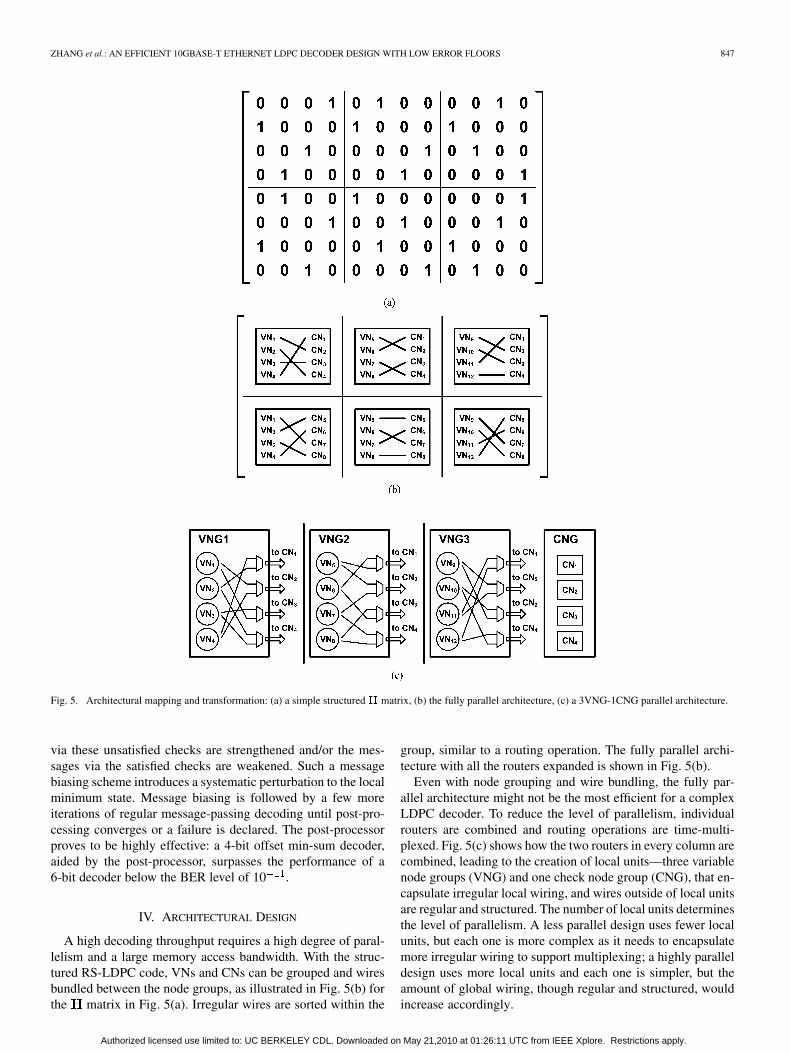
Fig. 5. Architectural mapping and transformation: (a) a simple structured� matrix, (b) the fully parallel architecture, (c) a 3VNG-1CNG parallel architecture.
via these unsatisfied checks are strengthened and/or the mes-sages via the satisfied checks are weakened. Such a messagebiasing scheme introduces a systematic perturbation to the localminimum state. Message biasing is followed by a few moreiterations of regular message-passing decoding until post-pro-cessing converges or a failure is declared. The post-processorproves to be highly effective: a 4-bit offset min-sum decoder,aided by the post-processor, surpasses the performance of a6-bit decoder below the BER level of 10 .
IV. ARCHITECTURAL DESIGN
A high decoding throughput requires a high degree of paral-lelism and a large memory access bandwidth. With the struc-tured RS-LDPC code, VNs and CNs can be grouped and wiresbundled between the node groups, as illustrated in Fig. 5(b) forthe matrix in Fig. 5(a). Irregular wires are sorted within the
group, similar to a routing operation. The fully parallel archi-tecture with all the routers expanded is shown in Fig. 5(b).
Even with node grouping and wire bundling, the fully par-allel architecture might not be the most efficient for a complexLDPC decoder. To reduce the level of parallelism, individualrouters are combined and routing operations are time-multi-plexed. Fig. 5(c) shows how the two routers in every column arecombined, leading to the creation of local units—three variablenode groups (VNG) and one check node group (CNG), that en-capsulate irregular local wiring, and wires outside of local unitsare regular and structured. The number of local units determinesthe level of parallelism. A less parallel design uses fewer localunits, but each one is more complex as it needs to encapsulatemore irregular wiring to support multiplexing; a highly paralleldesign uses more local units and each one is simpler, but theamount of global wiring, though regular and structured, wouldincrease accordingly.
Authorized licensed use limited to: UC BERKELEY CDL. Downloaded on May 21,2010 at 01:26:11 UTC from IEEE Xplore. Restrictions apply.
848 IEEE JOURNAL OF SOLID-STATE CIRCUITS, VOL. 45, NO. 4, APRIL 2010
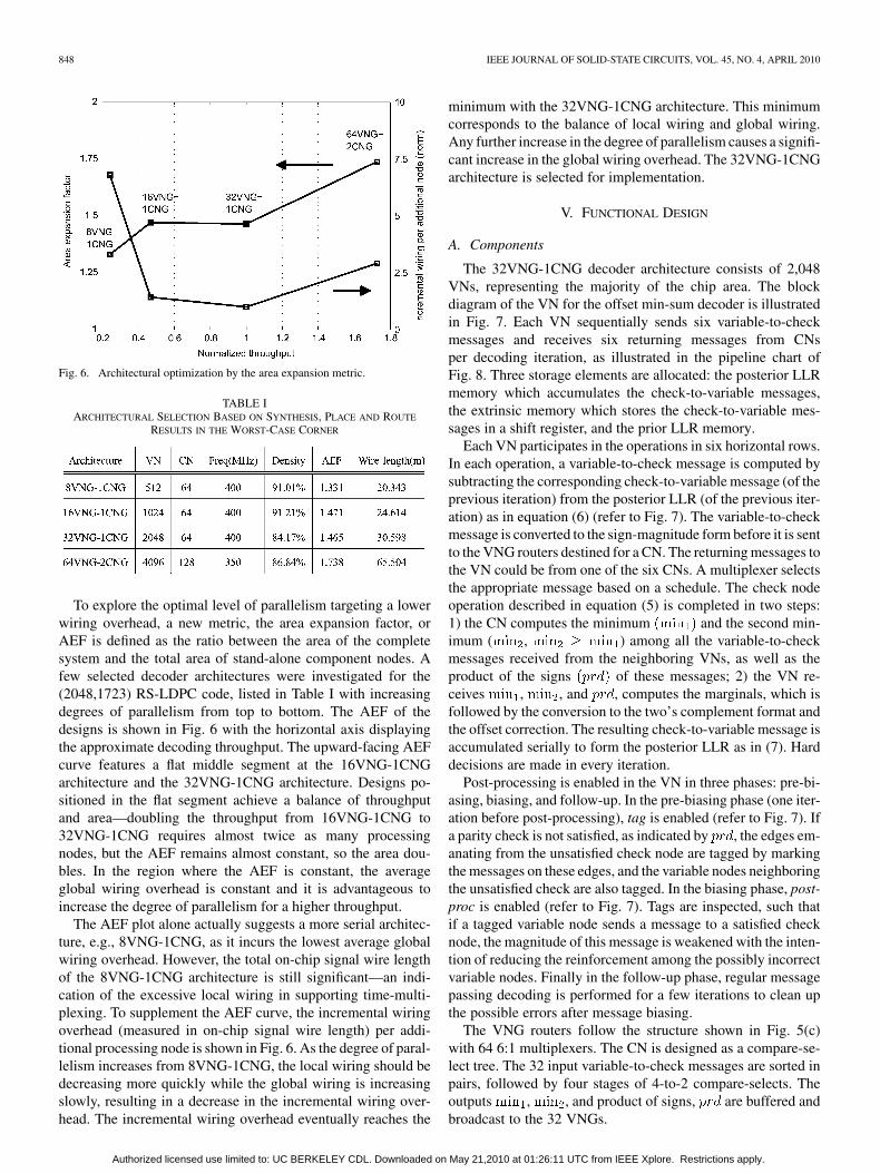
Fig. 6. Architectural optimization by the area expansion metric.
TABLE IARCHITECTURAL SELECTION BASED ON SYNTHESIS, PLACE AND ROUTE
RESULTS IN THE WORST-CASE CORNER
To explore the optimal level of parallelism targeting a lowerwiring overhead, a new metric, the area expansion factor, orAEF is defined as the ratio between the area of the completesystem and the total area of stand-alone component nodes. Afew selected decoder architectures were investigated for the(2048,1723) RS-LDPC code, listed in Table I with increasingdegrees of parallelism from top to bottom. The AEF of thedesigns is shown in Fig. 6 with the horizontal axis displayingthe approximate decoding throughput. The upward-facing AEFcurve features a flat middle segment at the 16VNG-1CNGarchitecture and the 32VNG-1CNG architecture. Designs po-sitioned in the flat segment achieve a balance of throughputand area—doubling the throughput from 16VNG-1CNG to32VNG-1CNG requires almost twice as many processingnodes, but the AEF remains almost constant, so the area dou-bles. In the region where the AEF is constant, the averageglobal wiring overhead is constant and it is advantageous toincrease the degree of parallelism for a higher throughput.
The AEF plot alone actually suggests a more serial architec-ture, e.g., 8VNG-1CNG, as it incurs the lowest average globalwiring overhead. However, the total on-chip signal wire lengthof the 8VNG-1CNG architecture is still significant—an indi-cation of the excessive local wiring in supporting time-multi-plexing. To supplement the AEF curve, the incremental wiringoverhead (measured in on-chip signal wire length) per addi-tional processing node is shown in Fig. 6. As the degree of paral-lelism increases from 8VNG-1CNG, the local wiring should bedecreasing more quickly while the global wiring is increasingslowly, resulting in a decrease in the incremental wiring over-head. The incremental wiring overhead eventually reaches the
minimum with the 32VNG-1CNG architecture. This minimumcorresponds to the balance of local wiring and global wiring.Any further increase in the degree of parallelism causes a signifi-cant increase in the global wiring overhead. The 32VNG-1CNGarchitecture is selected for implementation.
V. FUNCTIONAL DESIGN
A. Components
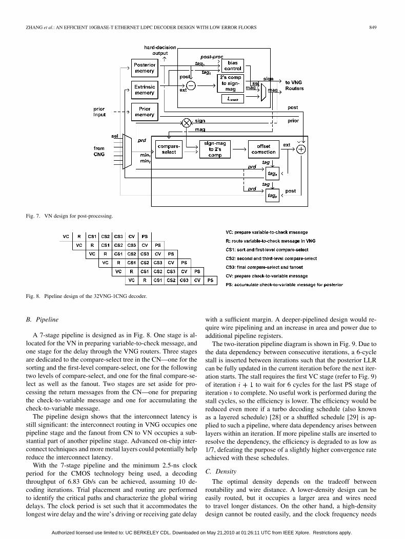
The 32VNG-1CNG decoder architecture consists of 2,048VNs, representing the majority of the chip area. The blockdiagram of the VN for the offset min-sum decoder is illustratedin Fig. 7. Each VN sequentially sends six variable-to-checkmessages and receives six returning messages from CNsper decoding iteration, as illustrated in the pipeline chart ofFig. 8. Three storage elements are allocated: the posterior LLRmemory which accumulates the check-to-variable messages,the extrinsic memory which stores the check-to-variable mes-sages in a shift register, and the prior LLR memory.
Each VN participates in the operations in six horizontal rows.In each operation, a variable-to-check message is computed bysubtracting the corresponding check-to-variable message (of theprevious iteration) from the posterior LLR (of the previous iter-ation) as in equation (6) (refer to Fig. 7). The variable-to-checkmessage is converted to the sign-magnitude form before it is sentto the VNG routers destined for a CN. The returning messages tothe VN could be from one of the six CNs. A multiplexer selectsthe appropriate message based on a schedule. The check nodeoperation described in equation (5) is completed in two steps:1) the CN computes the minimum and the second min-imum ( , ) among all the variable-to-checkmessages received from the neighboring VNs, as well as theproduct of the signs of these messages; 2) the VN re-ceives , , and , computes the marginals, which isfollowed by the conversion to the two’s complement format andthe offset correction. The resulting check-to-variable message isaccumulated serially to form the posterior LLR as in (7). Harddecisions are made in every iteration.
Post-processing is enabled in the VN in three phases: pre-bi-asing, biasing, and follow-up. In the pre-biasing phase (one iter-ation before post-processing), tag is enabled (refer to Fig. 7). Ifa parity check is not satisfied, as indicated by , the edges em-anating from the unsatisfied check node are tagged by markingthe messages on these edges, and the variable nodes neighboringthe unsatisfied check are also tagged. In the biasing phase, post-proc is enabled (refer to Fig. 7). Tags are inspected, such thatif a tagged variable node sends a message to a satisfied checknode, the magnitude of this message is weakened with the inten-tion of reducing the reinforcement among the possibly incorrectvariable nodes. Finally in the follow-up phase, regular messagepassing decoding is performed for a few iterations to clean upthe possible errors after message biasing.
The VNG routers follow the structure shown in Fig. 5(c)with 64 6:1 multiplexers. The CN is designed as a compare-se-lect tree. The 32 input variable-to-check messages are sorted inpairs, followed by four stages of 4-to-2 compare-selects. Theoutputs , , and product of signs, are buffered andbroadcast to the 32 VNGs.
Authorized licensed use limited to: UC BERKELEY CDL. Downloaded on May 21,2010 at 01:26:11 UTC from IEEE Xplore. Restrictions apply.
ZHANG et al.: AN EFFICIENT 10GBASE-T ETHERNET LDPC DECODER DESIGN WITH LOW ERROR FLOORS 849
Fig. 7. VN design for post-processing.
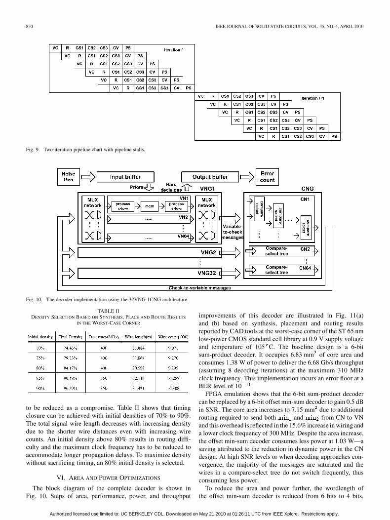
Fig. 8. Pipeline design of the 32VNG-1CNG decoder.
B. Pipeline
A 7-stage pipeline is designed as in Fig. 8. One stage is al-located for the VN in preparing variable-to-check message, andone stage for the delay through the VNG routers. Three stagesare dedicated to the compare-select tree in the CN—one for thesorting and the first-level compare-select, one for the followingtwo levels of compare-select, and one for the final compare-se-lect as well as the fanout. Two stages are set aside for pro-cessing the return messages from the CN—one for preparingthe check-to-variable message and one for accumulating thecheck-to-variable message.
The pipeline design shows that the interconnect latency isstill significant: the interconnect routing in VNG occupies onepipeline stage and the fanout from CN to VN occupies a sub-stantial part of another pipeline stage. Advanced on-chip inter-connect techniques and more metal layers could potentially helpreduce the interconnect latency.
With the 7-stage pipeline and the minimum 2.5-ns clockperiod for the CMOS technology being used, a decodingthroughput of 6.83 Gb/s can be achieved, assuming 10 de-coding iterations. Trial placement and routing are performedto identify the critical paths and characterize the global wiringdelays. The clock period is set such that it accommodates thelongest wire delay and the wire’s driving or receiving gate delay
with a sufficient margin. A deeper-pipelined design would re-quire wire pipelining and an increase in area and power due toadditional pipeline registers.
The two-iteration pipeline diagram is shown in Fig. 9. Due tothe data dependency between consecutive iterations, a 6-cyclestall is inserted between iterations such that the posterior LLRcan be fully updated in the current iteration before the next iter-ation starts. The stall requires the first VC stage (refer to Fig. 9)of iteration to wait for 6 cycles for the last PS stage ofiteration to complete. No useful work is performed during thestall cycles, so the efficiency is lower. The efficiency would bereduced even more if a turbo decoding schedule (also knownas a layered schedule) [28] or a shuffled schedule [29] is ap-plied to such a pipeline, where data dependency arises betweenlayers within an iteration. If more pipeline stalls are inserted toresolve the dependency, the efficiency is degraded to as low as1/7, defeating the purpose of a slightly higher convergence rateachieved with these schedules.
C. Density
The optimal density depends on the tradeoff betweenroutability and wire distance. A lower-density design can beeasily routed, but it occupies a larger area and wires needto travel longer distances. On the other hand, a high-densitydesign cannot be routed easily, and the clock frequency needs
Authorized licensed use limited to: UC BERKELEY CDL. Downloaded on May 21,2010 at 01:26:11 UTC from IEEE Xplore. Restrictions apply.
850 IEEE JOURNAL OF SOLID-STATE CIRCUITS, VOL. 45, NO. 4, APRIL 2010
Fig. 9. Two-iteration pipeline chart with pipeline stalls.
Fig. 10. The decoder implementation using the 32VNG-1CNG architecture.
TABLE IIDENSITY SELECTION BASED ON SYNTHESIS, PLACE AND ROUTE RESULTS
IN THE WORST-CASE CORNER
to be reduced as a compromise. Table II shows that timingclosure can be achieved with initial densities of 70% to 90%.The total signal wire length decreases with increasing densitydue to the shorter wire distances even with increasing wirecounts. An initial density above 80% results in routing diffi-culty and the maximum clock frequency has to be reduced toaccommodate longer propagation delays. To maximize densitywithout sacrificing timing, an 80% initial density is selected.
VI. AREA AND POWER OPTIMIZATIONS
The block diagram of the complete decoder is shown inFig. 10. Steps of area, performance, power, and throughput
improvements of this decoder are illustrated in Fig. 11(a)and (b) based on synthesis, placement and routing resultsreported by CAD tools at the worst-case corner of the ST 65 nmlow-power CMOS standard cell library at 0.9 V supply voltageand temperature of 105 C. The baseline design is a 6-bitsum-product decoder. It occupies 6.83 mm of core area andconsumes 1.38 W of power to deliver the 6.68 Gb/s throughput(assuming 8 decoding iterations) at the maximum 310 MHzclock frequency. This implementation incurs an error floor at aBER level of 10 .
FPGA emulation shows that the 6-bit sum-product decodercan be replaced by a 6-bit offset min-sum decoder to gain 0.5 dBin SNR. The core area increases to 7.15 mm due to additionalrouting required to send both and from CN to VNand this overhead is reflected in the 15.6% increase in wiring anda lower clock frequency of 300 MHz. Despite the area increase,the offset min-sum decoder consumes less power at 1.03 W—asaving attributed to the reduction in dynamic power in the CNdesign. At high SNR levels or when decoding approaches con-vergence, the majority of the messages are saturated and thewires in a compare-select tree do not switch frequently, thusconsuming less power.
To reduce the area and power further, the wordlength ofthe offset min-sum decoder is reduced from 6 bits to 4 bits.
Authorized licensed use limited to: UC BERKELEY CDL. Downloaded on May 21,2010 at 01:26:11 UTC from IEEE Xplore. Restrictions apply.
ZHANG et al.: AN EFFICIENT 10GBASE-T ETHERNET LDPC DECODER DESIGN WITH LOW ERROR FLOORS 851
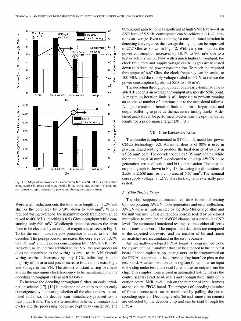
Fig. 11. Steps of improvement evaluated on the 32VNG-1CNG architectureusing synthesis, place and route results in the worst-case corner: (a) area andperformance improvement, (b) power and throughput improvement.
Wordlength reduction cuts the total wire length by 41.2% andshrinks the core area by 37.9% down to 4.44 mm . With areduced wiring overhead, the maximum clock frequency can beraised to 400 MHz, reaching a 8.53 Gb/s throughput while con-suming only 690 mW. Wordlength reduction causes the errorfloor to be elevated by an order of magnitude, as seen in Fig. 4.To fix the error floor, the post-processor is added to the 4-bitdecoder. The post-processor increases the core area by 13.7%to 5.05 mm and the power consumption by 17.6% to 810 mW.However, as an internal addition to the VN, the post-processordoes not contribute to the wiring external to the VN. Overallwiring overhead increases by only 1.7%, indicating that themajority of the area and power increase is due to the extra logicand storage in the VN. The almost constant wiring overheadallows the maximum clock frequency to be maintained, and thedecoding throughput is kept at 8.53 Gb/s.
To increase the decoding throughput further, an early termi-nation scheme [17], [19] is implemented on-chip to detect earlyconvergence by monitoring whether all the check nodes are sat-isfied and if so, the decoder can immediately proceed to thenext input frame. The early termination scheme eliminates idlecycles and the processing nodes are kept busy constantly. The
throughput gain becomes significant at high SNR levels—at anSNR level of 5.5 dB, convergence can be achieved in 1.47 itera-tions on average. Even accounting for one additional iteration indetecting convergence, the average throughput can be improvedto 27.7 Gb/s as shown in Fig. 12. With early termination, thepower consumption increases by 18.4% to 960 mW due to ahigher activity factor. Now with a much higher throughput, theclock frequency and supply voltage can be aggressively scaleddown to reduce the power consumption. To reach the requiredthroughput of 6.67 Gb/s, the clock frequency can be scaled to100 MHz and the supply voltage scaled to 0.7 V to reduce thepower consumption by almost 85% to 145 mW.
The decoding throughput quoted for an early-termination-en-abled decoder is an average throughput at a specific SNR point.A maximum iteration limit is still imposed to prevent runningan excessive number of iterations due to the occasional failures.A higher maximum iteration limit calls for a larger input andoutput buffering to provide the necessary timing slacks. A de-tailed analysis can be performed to determine the optimal bufferlength for a performance target [30], [31].
VII. CHIP IMPLEMENTATION
The decoder is implemented in ST 65 nm 7-metal low-powerCMOS technology [32]. An initial density of 80% is used inplacement and routing to produce the final density of 84.5% ina 5.35 mm core. The decoder occupies 5.05 mm of area, whilethe remaining 0.30 mm is dedicated to on-chip AWGN noisegeneration, error collection, and I/O compensation. The chip mi-crophotograph is shown in Fig. 13, featuring the dimensions of2.556 2.608 mm for a chip area of 6.67 mm . The nominalcore supply voltage is 1.2 V. The clock signal is externally gen-erated.
A. Chip Testing Setup
The chip supports automated, real-time functional testingby incorporating AWGN noise generators and error collection.AWGN noise is implemented by the Box-Muller algorithm andthe unit variance Gaussian random noise is scaled by pre-storedmultipliers to emulate an AWGN channel at a particular SNRlevel. The automated functional testing assumes either all-zerosor all-ones codeword. The output hard decisions are comparedto the expected codeword, and the number of bit and framemismatches are accumulated in the error counters.
An internally-developed FPGA board is programmed to bethe equivalent logic analyzer that can be attached to the chip testboard. In the simplest setup, the registers can be programmed onthe FPGA to connect to the corresponding interface pins to thetest board. A write operation to the register functions as an inputto the chip under test and a read functions as an output from thechip. This simplest form is used in automated testing, where thecontrol signals (start, load, reset) and configuration (limit on it-eration count, SNR level, limit on the number of input frames)are set via the FPGA board. The progress of decoding (numberof frames processed) can be monitored by polling the corre-sponding registers. Decoding results (bit and frame error counts)are collected by the decoder chip and can be read through theFPGA.
Authorized licensed use limited to: UC BERKELEY CDL. Downloaded on May 21,2010 at 01:26:11 UTC from IEEE Xplore. Restrictions apply.
852 IEEE JOURNAL OF SOLID-STATE CIRCUITS, VOL. 45, NO. 4, APRIL 2010
Fig. 12. Power reduction steps with results from synthesis, place and route in the worst-case corner.
Fig. 13. Chip microphotograph.
In a more elaborate testing scheme, the FPGA is programmedto generate the input data which are scanned in. A function-ally-equivalent LDPC decoder (of a much lower throughput dueto resource limitations) is programmed on the FPGA, whichruns concurrently with the decoder chip. The output from thechip through output scan chains is compared to the on-FPGAemulation to check for errors. This elaborate testing schemeenables more flexibility of operating on any codeword, how-ever the decoder needs to be paused in waiting for scan-in andscan-out to complete loading and unloading, resulting in a muchlower decoding throughput.
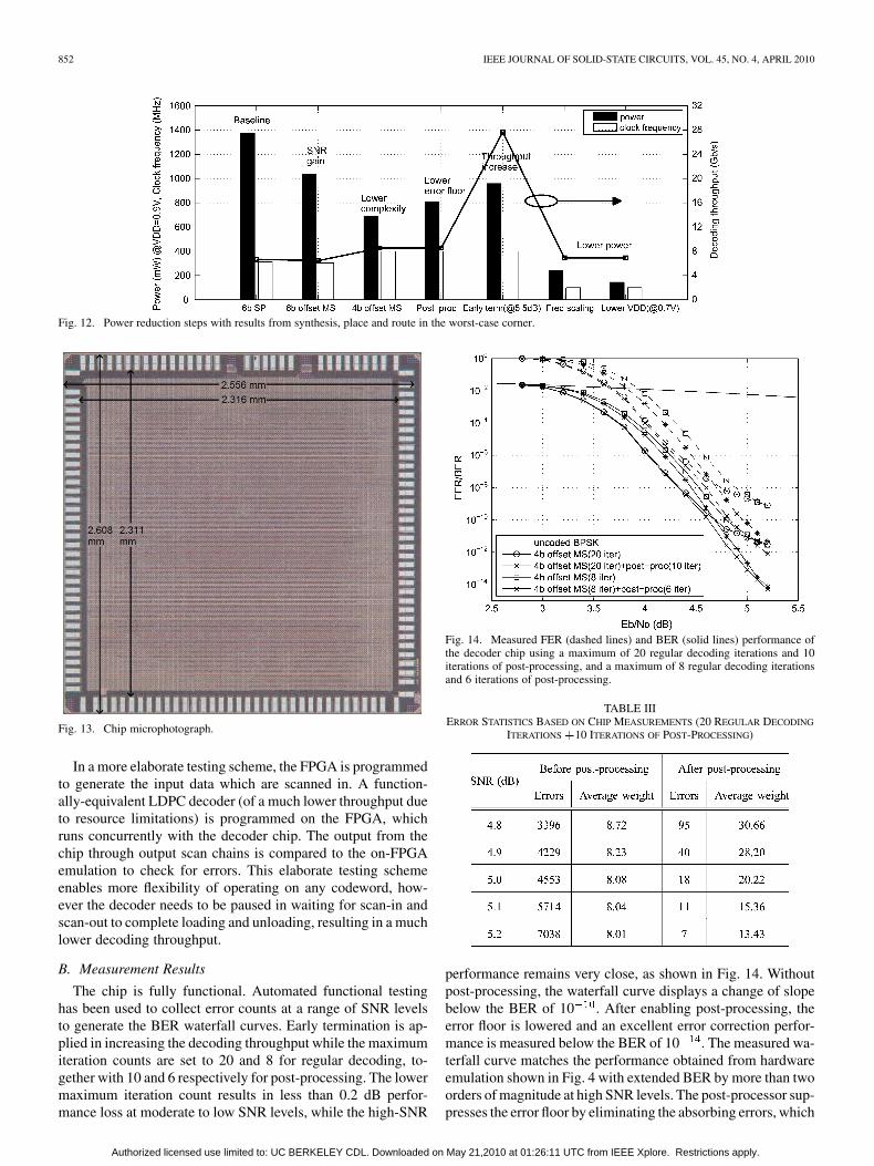
B. Measurement Results
The chip is fully functional. Automated functional testinghas been used to collect error counts at a range of SNR levelsto generate the BER waterfall curves. Early termination is ap-plied in increasing the decoding throughput while the maximumiteration counts are set to 20 and 8 for regular decoding, to-gether with 10 and 6 respectively for post-processing. The lowermaximum iteration count results in less than 0.2 dB perfor-mance loss at moderate to low SNR levels, while the high-SNR
Fig. 14. Measured FER (dashed lines) and BER (solid lines) performance ofthe decoder chip using a maximum of 20 regular decoding iterations and 10iterations of post-processing, and a maximum of 8 regular decoding iterationsand 6 iterations of post-processing.
TABLE IIIERROR STATISTICS BASED ON CHIP MEASUREMENTS (20 REGULAR DECODING
ITERATIONS �10 ITERATIONS OF POST-PROCESSING)
performance remains very close, as shown in Fig. 14. Withoutpost-processing, the waterfall curve displays a change of slopebelow the BER of 10 . After enabling post-processing, theerror floor is lowered and an excellent error correction perfor-mance is measured below the BER of 10 . The measured wa-terfall curve matches the performance obtained from hardwareemulation shown in Fig. 4 with extended BER by more than twoorders of magnitude at high SNR levels. The post-processor sup-presses the error floor by eliminating the absorbing errors, which
Authorized licensed use limited to: UC BERKELEY CDL. Downloaded on May 21,2010 at 01:26:11 UTC from IEEE Xplore. Restrictions apply.
ZHANG et al.: AN EFFICIENT 10GBASE-T ETHERNET LDPC DECODER DESIGN WITH LOW ERROR FLOORS 853
TABLE IVCONVERGENCE BEHAVIOR AND DECODING THROUGHPUT
is evident in Table III. Five of the seven unresolved errors at thelowest point on the curve are due to undetected errors—errorsthat are valid codewords, but not the intended codeword. It wasempirically discovered that the minimum distance is 14 for the(2048,1723) RS-LDPC code. The eventual elimination of ab-sorbing errors and the emergence of weight-14 undetected errorsindicate the near maximum-likelihood decoding performance.
The convergence behavior of the decoder is shown in Table IV.If the regular iteration count is limited to 8, the decoding con-verges in approximately 8, 7, and 4 iterations on average at SNRlevels of 3.0 dB, 3.5 dB, 4.0 dB respectively. For a lower errorfloor, post-processing is enabled when SNR reaches 4.5 dBor higher. Decoding of high-rate codes, e.g., the (2048,1723)RS-LDPC code, commonly requires far less number of itera-tions than low-rate codes [16] especially at moderate to highSNR levels. With an 8-iteration limit on regular decoding and a6-iteration limit on post-processing, the decoding converges inonly 2.6, 2, and 1.5 iterations on average at SNR levels of 4.5 dB,5.0 dB, and 5.5 dB, respectively. A higher maximum iterationcount of 20 on regular decoding and 10 on post-processingincreases the average convergence time at low SNR levels, butit has almost no effect on the average convergence time at highSNR levels (see Table IV), because only a small fraction of theinputs require the extra iterations for convergence. However ahigh maximum iteration count requires longer input and outputbuffers to accommodate the worst decoding latency.
For a BER of 10 or lower required by the 10GBASE-TEthernet standard, this decoder can be efficiently operated at anSNR of 5.0 dB. An extra margin of at least 0.5 dB is added dueto ingress noise. Fast convergence at the 5.5 dB SNR allowsmore time borrowing and effective throughput averaging amongthe average and worst cases. Buffers are added to handle thelong latency in decoding multiple successive frames corruptedby burst noise. Buffer size is an integral part of a decoder designemploying early termination and thorough discussions can befound in [30] and [31]. The number of iterations is practicallylimited by the buffer size in constant throughput applications.The maximum iteration count is therefore not limited by thedecoder architecture but by the choice of the buffer size.
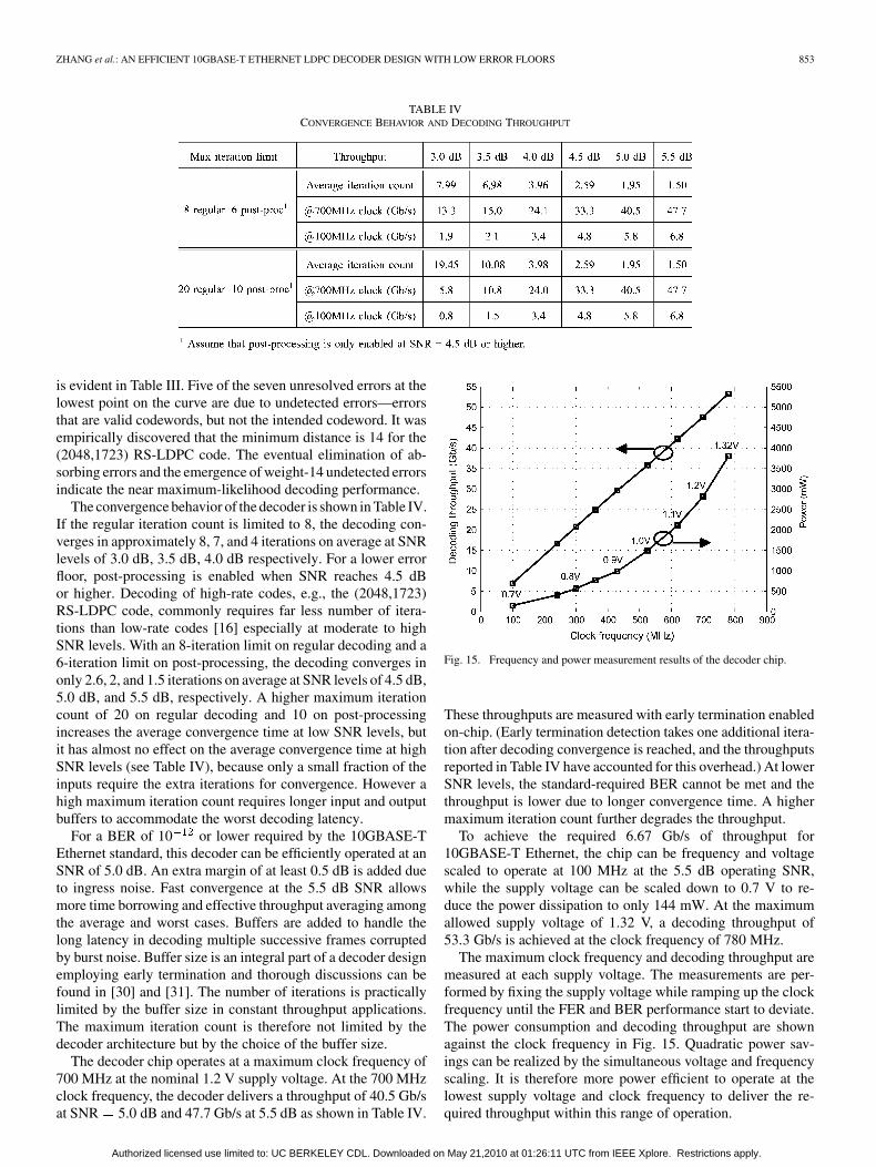
The decoder chip operates at a maximum clock frequency of700 MHz at the nominal 1.2 V supply voltage. At the 700 MHzclock frequency, the decoder delivers a throughput of 40.5 Gb/sat SNR 5.0 dB and 47.7 Gb/s at 5.5 dB as shown in Table IV.
Fig. 15. Frequency and power measurement results of the decoder chip.
These throughputs are measured with early termination enabledon-chip. (Early termination detection takes one additional itera-tion after decoding convergence is reached, and the throughputsreported in Table IV have accounted for this overhead.) At lowerSNR levels, the standard-required BER cannot be met and thethroughput is lower due to longer convergence time. A highermaximum iteration count further degrades the throughput.
To achieve the required 6.67 Gb/s of throughput for10GBASE-T Ethernet, the chip can be frequency and voltagescaled to operate at 100 MHz at the 5.5 dB operating SNR,while the supply voltage can be scaled down to 0.7 V to re-duce the power dissipation to only 144 mW. At the maximumallowed supply voltage of 1.32 V, a decoding throughput of53.3 Gb/s is achieved at the clock frequency of 780 MHz.
The maximum clock frequency and decoding throughput aremeasured at each supply voltage. The measurements are per-formed by fixing the supply voltage while ramping up the clockfrequency until the FER and BER performance start to deviate.The power consumption and decoding throughput are shownagainst the clock frequency in Fig. 15. Quadratic power sav-ings can be realized by the simultaneous voltage and frequencyscaling. It is therefore more power efficient to operate at thelowest supply voltage and clock frequency to deliver the re-quired throughput within this range of operation.
Authorized licensed use limited to: UC BERKELEY CDL. Downloaded on May 21,2010 at 01:26:11 UTC from IEEE Xplore. Restrictions apply.
854 IEEE JOURNAL OF SOLID-STATE CIRCUITS, VOL. 45, NO. 4, APRIL 2010
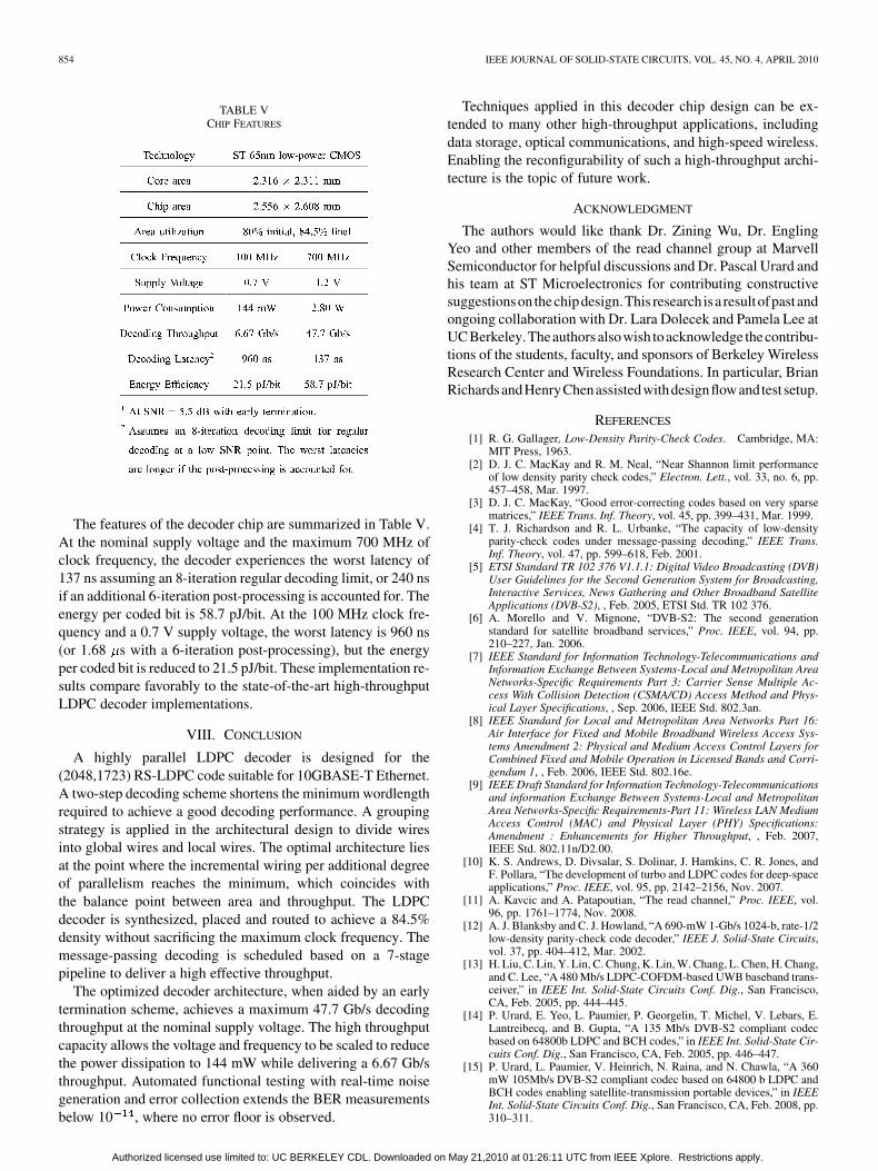
TABLE VCHIP FEATURES
The features of the decoder chip are summarized in Table V.At the nominal supply voltage and the maximum 700 MHz ofclock frequency, the decoder experiences the worst latency of137 ns assuming an 8-iteration regular decoding limit, or 240 nsif an additional 6-iteration post-processing is accounted for. Theenergy per coded bit is 58.7 pJ/bit. At the 100 MHz clock fre-quency and a 0.7 V supply voltage, the worst latency is 960 ns(or 1.68 s with a 6-iteration post-processing), but the energyper coded bit is reduced to 21.5 pJ/bit. These implementation re-sults compare favorably to the state-of-the-art high-throughputLDPC decoder implementations.
VIII. CONCLUSION
A highly parallel LDPC decoder is designed for the(2048,1723) RS-LDPC code suitable for 10GBASE-T Ethernet.A two-step decoding scheme shortens the minimum wordlengthrequired to achieve a good decoding performance. A groupingstrategy is applied in the architectural design to divide wiresinto global wires and local wires. The optimal architecture liesat the point where the incremental wiring per additional degreeof parallelism reaches the minimum, which coincides withthe balance point between area and throughput. The LDPCdecoder is synthesized, placed and routed to achieve a 84.5%density without sacrificing the maximum clock frequency. Themessage-passing decoding is scheduled based on a 7-stagepipeline to deliver a high effective throughput.
The optimized decoder architecture, when aided by an earlytermination scheme, achieves a maximum 47.7 Gb/s decodingthroughput at the nominal supply voltage. The high throughputcapacity allows the voltage and frequency to be scaled to reducethe power dissipation to 144 mW while delivering a 6.67 Gb/sthroughput. Automated functional testing with real-time noisegeneration and error collection extends the BER measurementsbelow 10 , where no error floor is observed.
Techniques applied in this decoder chip design can be ex-tended to many other high-throughput applications, includingdata storage, optical communications, and high-speed wireless.Enabling the reconfigurability of such a high-throughput archi-tecture is the topic of future work.
ACKNOWLEDGMENT
The authors would like thank Dr. Zining Wu, Dr. EnglingYeo and other members of the read channel group at MarvellSemiconductor for helpful discussions and Dr. Pascal Urard andhis team at ST Microelectronics for contributing constructivesuggestionson thechipdesign.This research isa resultofpastandongoing collaboration with Dr. Lara Dolecek and Pamela Lee atUCBerkeley.Theauthorsalsowish toacknowledge thecontribu-tions of the students, faculty, and sponsors of Berkeley WirelessResearch Center and Wireless Foundations. In particular, BrianRichardsandHenryChenassistedwithdesignflowandtest setup.
REFERENCES
[1] R. G. Gallager, Low-Density Parity-Check Codes. Cambridge, MA:MIT Press, 1963.
[2] D. J. C. MacKay and R. M. Neal, “Near Shannon limit performanceof low density parity check codes,” Electron. Lett., vol. 33, no. 6, pp.457–458, Mar. 1997.
[3] D. J. C. MacKay, “Good error-correcting codes based on very sparsematrices,” IEEE Trans. Inf. Theory, vol. 45, pp. 399–431, Mar. 1999.
[4] T. J. Richardson and R. L. Urbanke, “The capacity of low-densityparity-check codes under message-passing decoding,” IEEE Trans.Inf. Theory, vol. 47, pp. 599–618, Feb. 2001.
[5] ETSI Standard TR 102 376 V1.1.1: Digital Video Broadcasting (DVB)User Guidelines for the Second Generation System for Broadcasting,Interactive Services, News Gathering and Other Broadband SatelliteApplications (DVB-S2), , Feb. 2005, ETSI Std. TR 102 376.
[6] A. Morello and V. Mignone, “DVB-S2: The second generationstandard for satellite broadband services,” Proc. IEEE, vol. 94, pp.210–227, Jan. 2006.
[7] IEEE Standard for Information Technology-Telecommunications andInformation Exchange Between Systems-Local and Metropolitan AreaNetworks-Specific Requirements Part 3: Carrier Sense Multiple Ac-cess With Collision Detection (CSMA/CD) Access Method and Phys-ical Layer Specifications, , Sep. 2006, IEEE Std. 802.3an.
[8] IEEE Standard for Local and Metropolitan Area Networks Part 16:Air Interface for Fixed and Mobile Broadband Wireless Access Sys-tems Amendment 2: Physical and Medium Access Control Layers forCombined Fixed and Mobile Operation in Licensed Bands and Corri-gendum 1, , Feb. 2006, IEEE Std. 802.16e.
[9] IEEE Draft Standard for Information Technology-Telecommunicationsand information Exchange Between Systems-Local and MetropolitanArea Networks-Specific Requirements-Part 11: Wireless LAN MediumAccess Control (MAC) and Physical Layer (PHY) Specifications:Amendment : Enhancements for Higher Throughput, , Feb. 2007,IEEE Std. 802.11n/D2.00.
[10] K. S. Andrews, D. Divsalar, S. Dolinar, J. Hamkins, C. R. Jones, andF. Pollara, “The development of turbo and LDPC codes for deep-spaceapplications,” Proc. IEEE, vol. 95, pp. 2142–2156, Nov. 2007.
[11] A. Kavcic and A. Patapoutian, “The read channel,” Proc. IEEE, vol.96, pp. 1761–1774, Nov. 2008.
[12] A. J. Blanksby and C. J. Howland, “A 690-mW 1-Gb/s 1024-b, rate-1/2low-density parity-check code decoder,” IEEE J. Solid-State Circuits,vol. 37, pp. 404–412, Mar. 2002.
[13] H. Liu, C. Lin, Y. Lin, C. Chung, K. Lin, W. Chang, L. Chen, H. Chang,and C. Lee, “A 480 Mb/s LDPC-COFDM-based UWB baseband trans-ceiver,” in IEEE Int. Solid-State Circuits Conf. Dig., San Francisco,CA, Feb. 2005, pp. 444–445.
[14] P. Urard, E. Yeo, L. Paumier, P. Georgelin, T. Michel, V. Lebars, E.Lantreibecq, and B. Gupta, “A 135 Mb/s DVB-S2 compliant codecbased on 64800b LDPC and BCH codes,” in IEEE Int. Solid-State Cir-cuits Conf. Dig., San Francisco, CA, Feb. 2005, pp. 446–447.
[15] P. Urard, L. Paumier, V. Heinrich, N. Raina, and N. Chawla, “A 360mW 105Mb/s DVB-S2 compliant codec based on 64800 b LDPC andBCH codes enabling satellite-transmission portable devices,” in IEEEInt. Solid-State Circuits Conf. Dig., San Francisco, CA, Feb. 2008, pp.310–311.
Authorized licensed use limited to: UC BERKELEY CDL. Downloaded on May 21,2010 at 01:26:11 UTC from IEEE Xplore. Restrictions apply.
ZHANG et al.: AN EFFICIENT 10GBASE-T ETHERNET LDPC DECODER DESIGN WITH LOW ERROR FLOORS 855
[16] E. Yeo and B. Nikolic, “A 1.1-Gb/s 4092-bit low-density parity-checkdecoder,” in Proc. IEEE Asian Solid-State Circuits Conf., Hsinchu,Taiwan, Nov. 2005, pp. 237–240.
[17] X. Shih, C. Zhan, C. Lin, and A. Wu, “A ����mm 52 mW multi-modeLDPC decoder design for mobile WiMAX system in ���� �m CMOSprocess,” IEEE J. Solid-State Circuits, vol. 43, pp. 672–683, Mar. 2008.
[18] M. M. Mansour and N. R. Shanbhag, “A 640-Mb/s 2048-bit pro-grammable LDPC decoder chip,” IEEE J. Solid- State Circuits, vol.41, pp. 684–698, Mar. 2006.
[19] A. Darabiha, A. C. Carusone, and F. R. Kschischang, “Power reductiontechniques for LDPC decoders,” IEEE J. Solid-State Circuits, vol. 43,pp. 1835–1845, Aug. 2008.
[20] T. Richardson, “Error floors of LDPC codes,” in Proc. Allerton Conf.Communication, Control, and Computing, Monticello, IL, Oct. 2003,pp. 1426–1435.
[21] Z. Zhang, L. Dolecek, B. Nikolic, V. Anantharam, and M. J. Wainwright,“Lowering LDPC error floors by postprocessing,” in Proc. IEEE GlobalCommunications Conf., New Orleans, LA, Nov. 2008, pp. 1–6.
[22] Z. Zhang, “Design of LDPC decoders for improved low error rate per-formance,” Ph.D. dissertation, University of California, Berkeley, CA,2009.
[23] J. Hagenauer, E. Offer, and L. Papke, “Iterative decoding of binaryblock and convolutional codes,” IEEE Trans. Inf. Theory, vol. 42, pp.429–445, Mar. 1996.
[24] M. P. C. Fossorier, M. Mihaljevic, and H. Imai, “Reduced complexityiterative decoding of low-density parity check codes based on beliefpropagation,” IEEE Trans. Commun., vol. 47, pp. 673–680, May 1999.
[25] J. Chen, A. Dholakia, E. Eleftheriou, M. P. C. Fossorier, and X.Hu, “Reduced-complexity decoding of LDPC codes,” IEEE Trans.Commun., vol. 53, pp. 1288–1299, Aug. 2005.
[26] I. Djurdjevic, J. Xu, K. Abdel-Ghaffar, and S. Lin, “A class oflow-density parity-check codes constructed based on Reed–Solomoncodes with two information symbols,” IEEE Commun. Lett., vol. 7,pp. 317–319, Jul. 2003.
[27] Z. Zhang, L. Dolecek, B. Nikolic, V. Anantharam, and M. J. Wain-wright, “Design of LDPC decoders for improved low error rate perfor-mance: Quantization and algorithm choices,” IEEE Trans. Commun.,vol. 57, pp. 3258–3268, Nov. 2009.
[28] M. M. Mansour and N. R. Shanbhag, “Turbo decoder architectures forlow-density parity-check codes,” in Proc. IEEE Global Communica-tions Conf., Taipei, Taiwan, Nov. 2002, pp. 1383–1388.
[29] J. Zhang and M. P. C. Fossorier, “Shuffled iterative decoding,” IEEETrans. Commun., vol. 53, pp. 209–213, Feb. 2005.
[30] G. Bosco, G. Montorsi, and S. Benedetto, “Decreasing the complexityof LDPC iterative decoders,” IEEE Commun. Lett., vol. 9, no. 7, pp.634–636, Jul. 2005.
[31] M. Rovini and A. Martinez, “On the addition of an input buffer to an it-erative decoder for LDPC codes,” in Proc. IEEE Vehicular TechnologyConf., Dublin, Ireland, Apr. 2007, pp. 1995–1999.
[32] Z. Zhang, V. Anantharam, M. J. Wainwright, and B. Nikolic, “A 47Gb/s LDPC decoder with improved low error rate performance,” inSymp. VLSI Circuits Dig., Kyoto, Japan, Jun. 2009, pp. 286–287.
Zhengya Zhang (S’02–M’09) received the B.A.Sc.degree in computer engineering from the Universityof Waterloo, Waterloo, ON, Canada, in 2003, and theM.S. and Ph.D. degrees in electrical engineering fromthe University of California, Berkeley, in 2005 and2009, respectively.
In September 2009, he joined the University ofMichigan, Ann Arbor as an Assistant Professor in theDepartment of Electrical Engineering and ComputerScience. His research interest is in energy-efficientcommunications and signal processing system
design that spans algorithm design and analysis, architectural optimization, andefficient hardware implementation.
Dr. Zhang received the David J. Sakrison Memorial Prize for the mostoutstanding doctoral research in the Department of Electrical Engineering andComputer Sciences at the University of California, Berkeley, in 2009. He isalso the recipient of the Analog Devices Outstanding Student Designer Awardand the Vodafone U.S. Foundation Fellowship for his graduate research.
Venkat Anantharam (M’86–SM’96–F’98) receivedthe B.Tech. degree in electronics in 1980 from theIndian Institute of Technology, Madras (IIT-M), andthe M.A. and C.Phil. degrees in mathematics and theM.S. and Ph.D. degrees in electrical engineering in1983, 1984, 1982, and 1986, respectively, from theUniversity of California at Berkeley (UCB).
From 1986 to 1994 he was on the faculty of theSchool of Electrical Engineering at Cornell Univer-sity, Ithaca, NY. From 1994 he has been on the fac-ulty of the EECS department at UCB.
Dr. Anantharam received the Philips India Medal and the President of IndiaGold Medal from IIT-M in 1980, and an NSF Presidential Young Investigatoraward (1988–1993). He is a co-recipient of the 1998 Prize Paper award of theIEEE Information Theory Society (with S. Verdú) and a co-recipient of the2000 Stephen O. Rice Prize Paper award of the IEEE Communications TheorySociety (with N. Mckeown and J. Walrand). He received the DistinguishedAlumnus Award from IIT-M in 2008.
Martin Wainwright (M’03) received the Bachelorsdegree in mathematics from University of Waterloo,Canada, and the Ph.D. degree in electrical engi-neering and computer science from MassachusettsInstitute of Technology (MIT), Cambridge.
He is currently an Associate Professor at theUniversity of California at Berkeley, with a jointappointment between the Department of Statisticsand the Department of Electrical Engineering andComputer Sciences. His research interests includestatistical signal processing, coding and information
theory, statistical machine learning, and high-dimensional statistics.Dr. Wainwright has been awarded an Alfred P. Sloan Foundation Fellowship,
an NSF CAREER Award, the George M. Sprowls Prize for his dissertation re-search (EECS department, MIT), a Natural Sciences and Engineering ResearchCouncil of Canada 1967 Fellowship, an IEEE Signal Processing Society BestPaper Award in 2008, and several outstanding conference paper awards.
Borivoje Nikolic (S’93–M’99–SM’06) received theDipl.Ing. and M.Sc. degrees in electrical engineeringfrom the University of Belgrade, Serbia, in 1992 and1994, respectively, and the Ph.D. degree from theUniversity of California at Davis in 1999.
He lectured electronics courses at the Universityof Belgrade from 1992 to 1996. He spent twoyears with Silicon Systems, Inc., Texas InstrumentsStorage Products Group, San Jose, CA, working ondisk-drive signal processing electronics. In 1999, hejoined the Department of Electrical Engineering and
Computer Sciences, University of California at Berkeley, where he is now aProfessor. His research activities include digital and analog integrated circuitdesign and VLSI implementation of communications and signal processingalgorithms. He is coauthor of the book Digital Integrated Circuits: A DesignPerspective (2nd ed, Prentice-Hall, 2003).
Dr. Nikolic received the NSF CAREER award in 2003, College of Engi-neering Best Doctoral Dissertation Prize and Anil K. Jain Prize for the BestDoctoral Dissertation in Electrical and Computer Engineering at University ofCalifornia at Davis in 1999, as well as the City of Belgrade Award for theBest Diploma Thesis in 1992. For work with his students and colleagues he re-ceived the best paper awards at the ISSCC, ISLPED, and the International SOIConference.
Authorized licensed use limited to: UC BERKELEY CDL. Downloaded on May 21,2010 at 01:26:11 UTC from IEEE Xplore. Restrictions apply.