Embed Size (px)
Citation preview
IEEE TRANSACTIONS ON ADVANCED PACKAGING, VOL. 26, NO. 2, MAY 2003 141
Reliability Assessment of Delamination inChip-to-Chip Bonded MEMS Packaging
Rajesh Swaminathan, Harish Bhaskaran, Peter A. Sandborn, Senior Member, IEEE, Gowrishankar Subramanian,Michael A. Deeds, and Kevin R. Cochran
Abstract—The bond layer is often the weakest link in thereliability of chip packages in the integrated circuit (IC) industry.Micro-electrical-mechanical systems (MEMS) packages are noexception to this trend. This paper presents a nondestructivemethodology for determining delamination in chip-to-chip bondedMEMS. Experimental methods are used to determine the adhesivelayer strength in samples subjected to environmental testing, andthe reliability of the bonding layer is investigated. A simulation isperformed using inputs from scanning acoustic microscopy, andsimulation model results are correlated with the experimental dieshear measurements to establish the validity of the nondestructivemethodology for determining adhesive layer strength.
Index Terms—Chip-to-chip bonding, delamination, die shear,MEMS, MEMS packaging, reliability, scanning acoustic mi-croscopy.
I. INTRODUCTION
M ICRO-ELECTRO-MECHANICAL systems (MEMS)have found widespread applications in a variety of fields
ranging from simple sensors to complex systems that requirethe integration of movable structures and active circuitry.Among the challenges associated with transitioning MEMSfrom the laboratory to the marketplace is packaging. Packagingencompasses the transition of an electronic or electromechan-ical device from the die to the final product, so that the device iscapable of functioning as part of a larger system. It includes, butis not limited to, the design of interconnections at every level ofthe system, the placement of the die in the package, removal ofexcessive heat generated in the case of integrated circuits (IC’s)and issues of reliability associated with the system as a whole[1]. A strong packaging background exists for microelectronicdevices, but research in MEMS packaging is still in its infancy.
MEMS are finding applications in products and systemsthat require reliable operation over extended periods of time.The reliability requirements for the final product encompass
Manuscript received September 6, 2002; revised June 13, 2003. This workwas supported by the Naval Surface Warfare Center, Indian Head, MD, and theCALCE Electronic Products and Systems Center, University of Maryland.
R. Swaminathan was with the CALCE Electronic Products and SystemsCenter, University of Maryland, College Park, MD 20742 USA, and is nowwith Bell Laboratories, Lucent Technologies, Holmdel, NJ 07733 USA (e-mail:[email protected]).
H. Bhaskaran and P. A. Sandborn are with the CALCE Electronic Productsand Systems Center, University of Maryland, College Park, MD 20742 USA.
G. Subramanian was with the CALCE Electronic Products and SystemsCenter at the University of Maryland, College Park, MD 20742 USA, and isnow with Advanced Micro Devices, Inc. Sunnyvale, CA 94088 USA (e-mail:[email protected]).
M. A. Deeds and K. R. Cochran are with the Indian Head Division, NavalSurface Warfare Center, Indian Head, MD 20640 USA.
Digital Object Identifier 10.1109/TADVP.2003.817344
both the mechanical behaviors and the electrical characteristicsof the overall system. One critical element in many MEMSapplications is chip-to-chip bonding (component bonding) [2],for which long-term operation and storage reliability needs tobe understood [3]. MEMS packages are likely to have a largenumber of bond layers because of multiple interfaces insidethe package. The bond layers in MEMS devices must oftenmaintain precise chip alignment in addition to withstandingloading from the macro-environment and loading within thepackage. A primary indicator of failure (or impending failure)in a chip-to-chip bonded system is delamination between thechip and the material used to bond the chips together [4]. Inspite of its importance in MEMS packaging, previous workon bonding in MEMS structures is limited [5]. Very littleMEMS-specific work on the reliability of the chip-to-chipbonds exists, let alone, nondestructive methods for determiningthe reliability of chip-to-chip bonded MEMS.
The use of acoustic micro imaging (AMI) in nondestructivereliability assessment of microelectronic devices is common.McCluskeyet al.[6] used AMI techniques to assess the delami-nation in plastic encapsulated microcircuits. Mahajan and Pecht[7] also describe the use of a scanning acoustic microscope(SAM) for delamination assessment. AMI techniques have beenused by Gunnamani and Munnamarty to asses the cracks insolder joints in flip-chip assemblies [8]. In MEMS structures,bonding has been studied previously using destructive testing[9], and AMI has been used to assess failures in tunneling ac-celerometers [10], but not applied to the assessment of bond re-liability. Herenzet al.proposed the use of ultrasonic techniquesusing AMI to check bond quality [11].
The results of a delamination study using nondestructive tech-niques on chip-to-chip bonding in a MEMS-based Safety andarming (S&A) system is described in this paper. A brief descrip-tion of the system is provided, the delamination measurementsand testing approaches are discussed, and results from accel-erated aging, thermal cycling, mechanical shock and die shearvalidation are presented. In Section V a finite element model isdeveloped and results from simulation of the die shear are com-pared with the experimental die shear results in order to under-stand and verify the delamination measurement methodology.
II. A MEMS-BASED SAFETY AND ARMING (S&A) SYSTEM
The application discussed in this paper is the safety andarming (S&A) device described in [12] and [13] for use inundersea torpedoes in which two chips containing MEMSstructures must be bonded together and operate reliably aftermany years of storage in extreme environmental conditions.
1521-3323/03$17.00 © 2003 IEEE
142 IEEE TRANSACTIONS ON ADVANCED PACKAGING, VOL. 26, NO. 2, MAY 2003
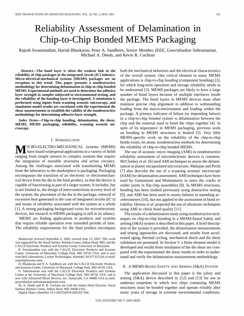
Fig. 1. MEMS S&A system showing details of various components.
This motivates the development of an experimental approachthat can accelerate relevant failure mechanisms and allow theevaluation of the system’s reliability. As previously mentioned,the reliability concern in this paper is the integrity of thechip-to-chip bonding layers. Non-destructive methods arepreferred to destructive testing in most IC applications, withdestructive testing serving as a verification of the nondestruc-tive testing techniques. This paper describes a nondestructiveapproach to measure delamination of the bond layers.
The requirements of the S&A system are to safely and reli-ably arm and detonate a weapon, but only after all safety cri-teria are met and the weapon has reached its intended target.The MEMS S&A system is shown in Fig. 1.
The MEMS components include the S&A chip, deflection de-limiter and the initiator chip. The operation and constructionof the S&A system has been discussed in [12]–[14], and pic-tures of the system can be found in [15]. The S&A chip pro-vides the explosive barrier, houses environmental sensors, andallows optical indication of device status. The silicon S&A chipis fabricated using a combination of surface and bulk microma-chining and requires no assembly. Parts are selectively releasedto achieve the desired combination of moving and fixed struc-tures.
In operation, as each environment is sensed, a lock is removedfrom a movable barrier (“slider”). Once all the locks have beenremoved and the fuze decides it is time to arm, the slider ismoved to expose a hole through the S&A chip so that the ex-plosive train may detonate.
The chip-level package includes the S&A, initiator chip,and delimiter. The initiator chip converts electrical energy tomechanical energy upon demand to start the explosive train.The initiator chip is also fabricated using MEMS technology.The S&A chip and the initiator chip must be reliably bondedtogether while maintaining precise in-plane and out-of-planealignment. Coefficients of thermal expansion mismatchbetween the S&A chip and the initiator chip increases the chal-
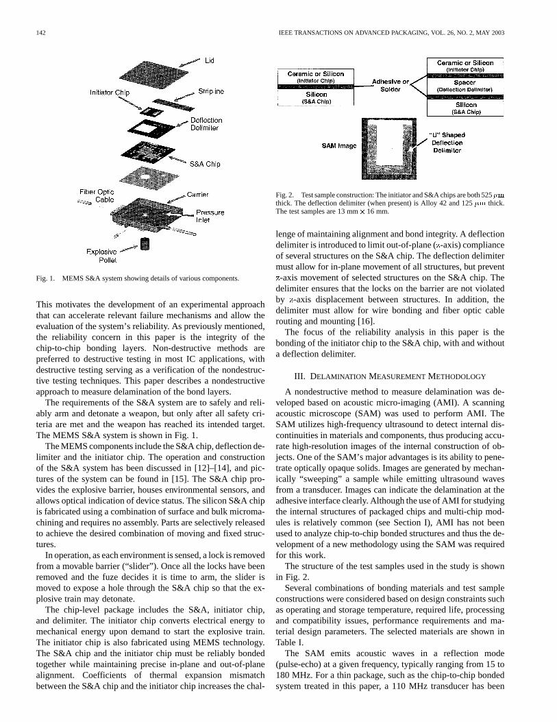
Fig. 2. Test sample construction: The initiator and S&A chips are both 525�m
thick. The deflection delimiter (when present) is Alloy 42 and 125�m thick.The test samples are 13 mm� 16 mm.
lenge of maintaining alignment and bond integrity. A deflectiondelimiter is introduced to limit out-of-plane (-axis) complianceof several structures on the S&A chip. The deflection delimitermust allow for in-plane movement of all structures, but prevent-axis movement of selected structures on the S&A chip. The
delimiter ensures that the locks on the barrier are not violatedby -axis displacement between structures. In addition, thedelimiter must allow for wire bonding and fiber optic cablerouting and mounting [16].
The focus of the reliability analysis in this paper is thebonding of the initiator chip to the S&A chip, with and withouta deflection delimiter.
III. D ELAMINATION MEASUREMENTMETHODOLOGY
A nondestructive method to measure delamination was de-veloped based on acoustic micro-imaging (AMI). A scanningacoustic microscope (SAM) was used to perform AMI. TheSAM utilizes high-frequency ultrasound to detect internal dis-continuities in materials and components, thus producing accu-rate high-resolution images of the internal construction of ob-jects. One of the SAM’s major advantages is its ability to pene-trate optically opaque solids. Images are generated by mechan-ically “sweeping” a sample while emitting ultrasound wavesfrom a transducer. Images can indicate the delamination at theadhesive interface clearly. Although the use of AMI for studyingthe internal structures of packaged chips and multi-chip mod-ules is relatively common (see Section I), AMI has not beenused to analyze chip-to-chip bonded structures and thus the de-velopment of a new methodology using the SAM was requiredfor this work.
The structure of the test samples used in the study is shownin Fig. 2.
Several combinations of bonding materials and test sampleconstructions were considered based on design constraints suchas operating and storage temperature, required life, processingand compatibility issues, performance requirements and ma-terial design parameters. The selected materials are shown inTable I.
The SAM emits acoustic waves in a reflection mode(pulse-echo) at a given frequency, typically ranging from 15 to180 MHz. For a thin package, such as the chip-to-chip bondedsystem treated in this paper, a 110 MHz transducer has been
SWAMINATHAN et al.: RELIABILITY ASSESSMENT OF DELAMINATION 143
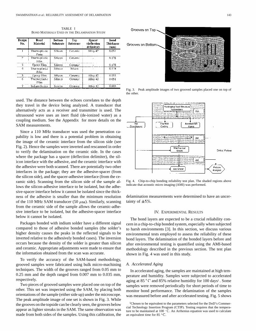
TABLE IBOND MATERIALS USED IN THE DELAMINATION STUDY
used. The distance between the echoes correlates to the depththey travel in the device being analyzed. A transducer thatalternatively acts as a receiver and transmitter is used. Theultrasound wave uses an inert fluid (de-ionized water) as acoupling medium. See the Appendix for more details on theSAM measurements.
Since a 110 MHz transducer was used the penetration ca-pability is low and there is a potential problem in obtainingthe image of the ceramic interface from the silicon side (seeFig. 2). Hence the samples were inverted and rescanned in orderto verify the delamination on the ceramic side. In the caseswhere the package has a spacer (deflection delimiter), the sil-icon interface with the adhesive, and the ceramic interface withthe adhesive were both scanned. There are potentially two otherinterfaces in the package; they are the adhesive-spacer (fromthe silicon side), and the spacer-adhesive interface (from the ce-ramic side). Scanning from the silicon side of the sample al-lows the silicon-adhesive interface to be isolated, but the adhe-sive-spacer interface below it cannot be isolated since the thick-ness of the adhesive is smaller than the minimum resolutionof the 110 MHz SAM transducer (50 ). Similarly, scanningfrom the ceramic side of the sample allows the ceramic-adhe-sive interface to be isolated, but the adhesive-spacer interfacebelow it cannot be isolated.
Packages bonded with indium solder have a different signalcompared to those of adhesive bonded samples (the solder’shigher density causes the peaks in the reflected signals to beinverted relative to the adhesively bonded cases). The inversionoccurs because the density of the solder is greater than siliconand ceramic. Appropriate adjustments were made to ensure thatthe information obtained from the scan was accurate.
To verify the accuracy of the SAM-based methodology,grooved samples were fabricated using bulk micro-machiningtechniques. The width of the grooves ranged from 0.05 mm to0.25 mm and the depth ranged from 0.007 mm to 0.035 mm,respectively.
Two pieces of grooved samples were placed one on top of theother. This set was inspected using the SAM, by placing bothorientations of the sample (either side up) under the microscope.The peak amplitude image of one set is shown in Fig. 3. Whilethe grooves on the topside can be clearly seen, the grooves belowappear as lighter streaks in the SAM. The same observation wasmade from both sides of the samples. Using this calibration, the
Fig. 3. Peak amplitude images of two grooved samples placed one on top ofthe other.
Fig. 4. Chip-to-chip bonding reliability test plan. The shaded regions aboveindicate that acoustic micro imaging (AMI) was performed.
delamination measurements were determined to have an uncer-tainty of .
IV. EXPERIMENTAL RESULTS
The bond layers are expected to be a crucial reliability con-cern in a chip-to-chip bonded system, especially when subjectedto harsh environments [3]. In this section, we discuss variousenvironmental tests employed to assess the reliability of thesebond layers. The delamination of the bonded layers before andafter environmental testing is quantified using the AMI-basedmethodology described in the previous section. The test planshown in Fig. 4 was used in this study.
A. Accelerated Aging
In accelerated aging, the samples are maintained at high tem-perature and humidity. Samples were subjected to acceleratedaging at 85 and 85% relative humidity for 100 days1 . Somesamples were removed periodically for short periods of time tomonitor bond performance. The delamination of the sampleswas measured before and after accelerated testing. Fig. 5 shows
1Chosen to be equivalent to the parameters selected for the DoD’s Commer-cial Technology Insertion Program (CTIP). Testing requires that the tempera-ture to be maintained at 100C. An Arrhenius equation was used to calculatean equivalent time for 85C.
144 IEEE TRANSACTIONS ON ADVANCED PACKAGING, VOL. 26, NO. 2, MAY 2003
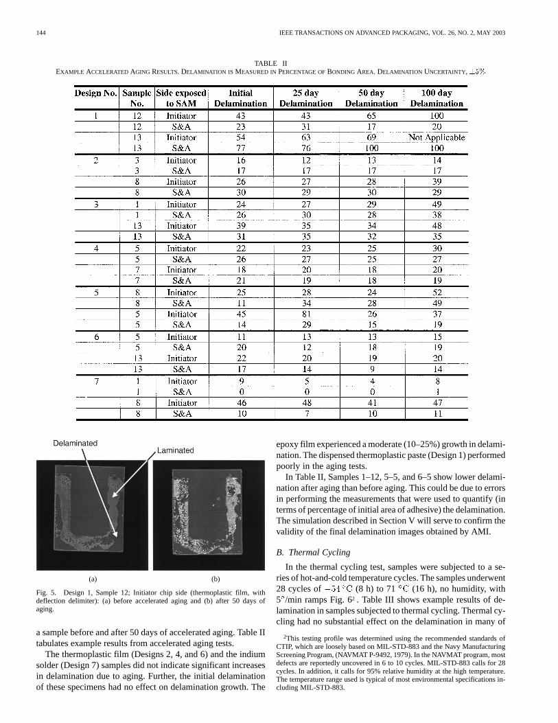
TABLE IIEXAMPLE ACCELERATEDAGING RESULTS. DELAMINATION IS MEASURED INPERCENTAGE OFBONDING AREA. DELAMINATION UNCERTAINTY,�5%
(a) (b)
Fig. 5. Design 1, Sample 12; Initiator chip side (thermoplastic film, withdeflection delimiter): (a) before accelerated aging and (b) after 50 days ofaging.
a sample before and after 50 days of accelerated aging. Table IItabulates example results from accelerated aging tests.
The thermoplastic film (Designs 2, 4, and 6) and the indiumsolder (Design 7) samples did not indicate significant increasesin delamination due to aging. Further, the initial delaminationof these specimens had no effect on delamination growth. The
epoxy film experienced a moderate (10–25%) growth in delami-nation. The dispensed thermoplastic paste (Design 1) performedpoorly in the aging tests.
In Table II, Samples 1–12, 5–5, and 6–5 show lower delami-nation after aging than before aging. This could be due to errorsin performing the measurements that were used to quantify (interms of percentage of initial area of adhesive) the delamination.The simulation described in Section V will serve to confirm thevalidity of the final delamination images obtained by AMI.
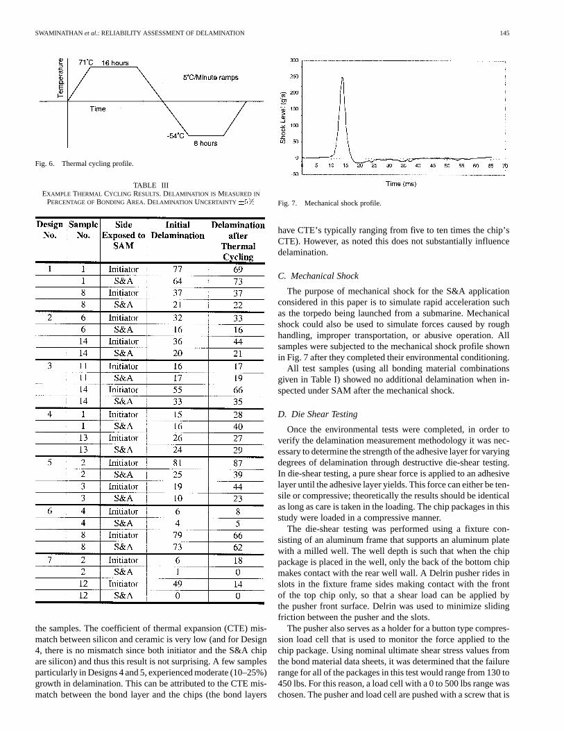
B. Thermal Cycling
In the thermal cycling test, samples were subjected to a se-ries of hot-and-cold temperature cycles. The samples underwent28 cycles of (8 h) to 71 (16 h), no humidity, with5 /min ramps Fig. 62 . Table III shows example results of de-lamination in samples subjected to thermal cycling. Thermal cy-cling had no substantial effect on the delamination in many of
2This testing profile was determined using the recommended standards ofCTIP, which are loosely based on MIL-STD-883 and the Navy ManufacturingScreening Program, (NAVMAT P-9492, 1979). In the NAVMAT program, mostdefects are reportedly uncovered in 6 to 10 cycles. MIL-STD-883 calls for 28cycles. In addition, it calls for 95% relative humidity at the high temperature.The temperature range used is typical of most environmental specifications in-cluding MIL-STD-883.
SWAMINATHAN et al.: RELIABILITY ASSESSMENT OF DELAMINATION 145
Fig. 6. Thermal cycling profile.
TABLE IIIEXAMPLE THERMAL CYCLING RESULTS. DELAMINATION IS MEASURED IN
PERCENTAGE OFBONDING AREA. DELAMINATION UNCERTAINTY �5%
the samples. The coefficient of thermal expansion (CTE) mis-match between silicon and ceramic is very low (and for Design4, there is no mismatch since both initiator and the S&A chipare silicon) and thus this result is not surprising. A few samplesparticularly in Designs 4 and 5, experienced moderate (10–25%)growth in delamination. This can be attributed to the CTE mis-match between the bond layer and the chips (the bond layers
Fig. 7. Mechanical shock profile.
have CTE’s typically ranging from five to ten times the chip’sCTE). However, as noted this does not substantially influencedelamination.
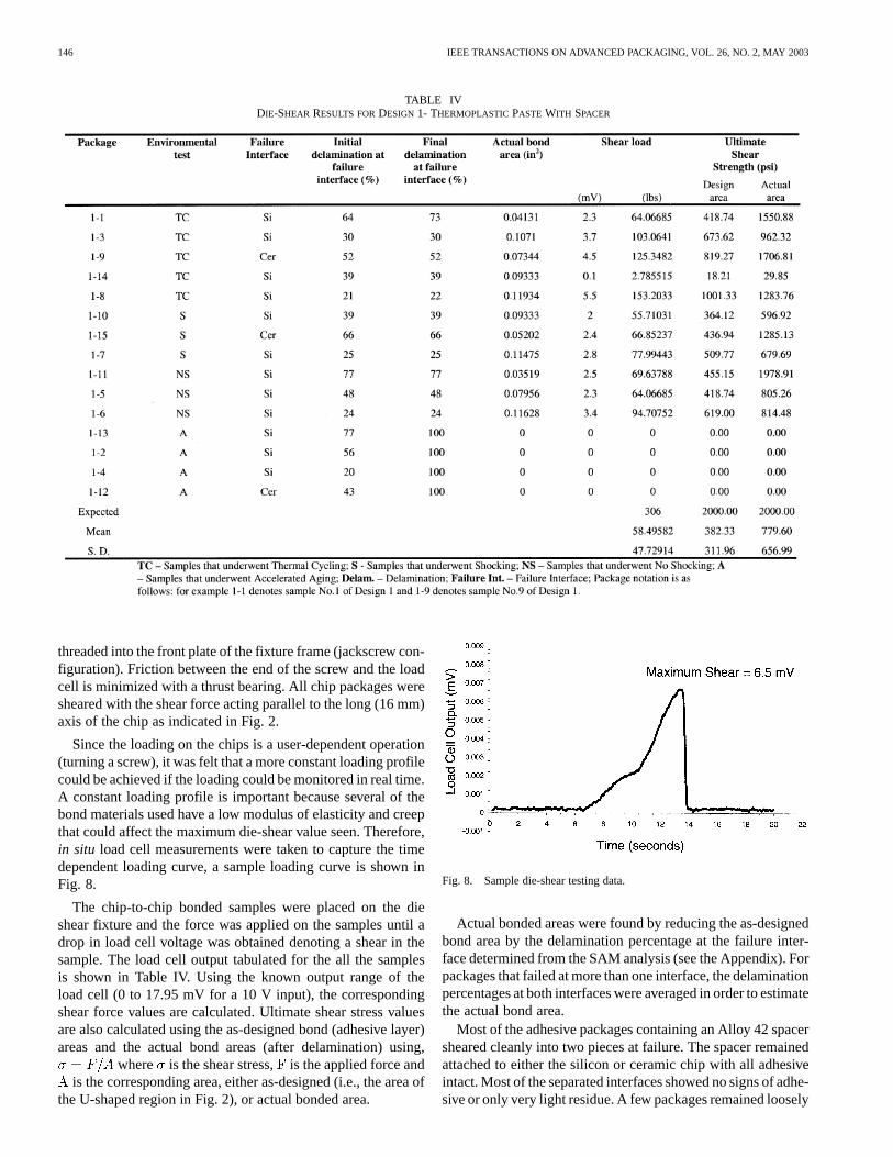
C. Mechanical Shock
The purpose of mechanical shock for the S&A applicationconsidered in this paper is to simulate rapid acceleration suchas the torpedo being launched from a submarine. Mechanicalshock could also be used to simulate forces caused by roughhandling, improper transportation, or abusive operation. Allsamples were subjected to the mechanical shock profile shownin Fig. 7 after they completed their environmental conditioning.
All test samples (using all bonding material combinationsgiven in Table I) showed no additional delamination when in-spected under SAM after the mechanical shock.
D. Die Shear Testing
Once the environmental tests were completed, in order toverify the delamination measurement methodology it was nec-essary to determine the strength of the adhesive layer for varyingdegrees of delamination through destructive die-shear testing.In die-shear testing, a pure shear force is applied to an adhesivelayer until the adhesive layer yields. This force can either be ten-sile or compressive; theoretically the results should be identicalas long as care is taken in the loading. The chip packages in thisstudy were loaded in a compressive manner.
The die-shear testing was performed using a fixture con-sisting of an aluminum frame that supports an aluminum platewith a milled well. The well depth is such that when the chippackage is placed in the well, only the back of the bottom chipmakes contact with the rear well wall. A Delrin pusher rides inslots in the fixture frame sides making contact with the frontof the top chip only, so that a shear load can be applied bythe pusher front surface. Delrin was used to minimize slidingfriction between the pusher and the slots.
The pusher also serves as a holder for a button type compres-sion load cell that is used to monitor the force applied to thechip package. Using nominal ultimate shear stress values fromthe bond material data sheets, it was determined that the failurerange for all of the packages in this test would range from 130 to450 lbs. For this reason, a load cell with a 0 to 500 lbs range waschosen. The pusher and load cell are pushed with a screw that is
146 IEEE TRANSACTIONS ON ADVANCED PACKAGING, VOL. 26, NO. 2, MAY 2003
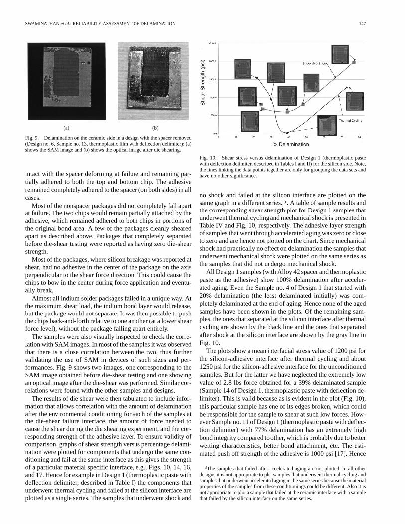
TABLE IVDIE-SHEAR RESULTS FORDESIGN 1- THERMOPLASTICPASTE WITH SPACER
threaded into the front plate of the fixture frame (jackscrew con-figuration). Friction between the end of the screw and the loadcell is minimized with a thrust bearing. All chip packages weresheared with the shear force acting parallel to the long (16 mm)axis of the chip as indicated in Fig. 2.
Since the loading on the chips is a user-dependent operation(turning a screw), it was felt that a more constant loading profilecould be achieved if the loading could be monitored in real time.A constant loading profile is important because several of thebond materials used have a low modulus of elasticity and creepthat could affect the maximum die-shear value seen. Therefore,in situ load cell measurements were taken to capture the timedependent loading curve, a sample loading curve is shown inFig. 8.
The chip-to-chip bonded samples were placed on the dieshear fixture and the force was applied on the samples until adrop in load cell voltage was obtained denoting a shear in thesample. The load cell output tabulated for the all the samplesis shown in Table IV. Using the known output range of theload cell (0 to 17.95 mV for a 10 V input), the correspondingshear force values are calculated. Ultimate shear stress valuesare also calculated using the as-designed bond (adhesive layer)areas and the actual bond areas (after delamination) using,
where is the shear stress,is the applied force andis the corresponding area, either as-designed (i.e., the area of
the U-shaped region in Fig. 2), or actual bonded area.
Fig. 8. Sample die-shear testing data.
Actual bonded areas were found by reducing the as-designedbond area by the delamination percentage at the failure inter-face determined from the SAM analysis (see the Appendix). Forpackages that failed at more than one interface, the delaminationpercentages at both interfaces were averaged in order to estimatethe actual bond area.
Most of the adhesive packages containing an Alloy 42 spacersheared cleanly into two pieces at failure. The spacer remainedattached to either the silicon or ceramic chip with all adhesiveintact. Most of the separated interfaces showed no signs of adhe-sive or only very light residue. A few packages remained loosely
SWAMINATHAN et al.: RELIABILITY ASSESSMENT OF DELAMINATION 147
(a) (b)
Fig. 9. Delamination on the ceramic side in a design with the spacer removed(Design no. 6, Sample no. 13, thermoplastic film with deflection delimiter): (a)shows the SAM image and (b) shows the optical image after die shearing.
intact with the spacer deforming at failure and remaining par-tially adhered to both the top and bottom chip. The adhesiveremained completely adhered to the spacer (on both sides) in allcases.
Most of the nonspacer packages did not completely fall apartat failure. The two chips would remain partially attached by theadhesive, which remained adhered to both chips in portions ofthe original bond area. A few of the packages cleanly shearedapart as described above. Packages that completely separatedbefore die-shear testing were reported as having zero die-shearstrength.
Most of the packages, where silicon breakage was reported atshear, had no adhesive in the center of the package on the axisperpendicular to the shear force direction. This could cause thechips to bow in the center during force application and eventu-ally break.
Almost all indium solder packages failed in a unique way. Atthe maximum shear load, the indium bond layer would release,but the package would not separate. It was then possible to pushthe chips back-and-forth relative to one another (at a lower shearforce level), without the package falling apart entirely.
The samples were also visually inspected to check the corre-lation with SAM images. In most of the samples it was observedthat there is a close correlation between the two, thus furthervalidating the use of SAM in devices of such sizes and per-formances. Fig. 9 shows two images, one corresponding to theSAM image obtained before die-shear testing and one showingan optical image after the die-shear was performed. Similar cor-relations were found with the other samples and designs.
The results of die shear were then tabulated to include infor-mation that allows correlation with the amount of delaminationafter the environmental conditioning for each of the samples atthe die-shear failure interface, the amount of force needed tocause the shear during the die shearing experiment, and the cor-responding strength of the adhesive layer. To ensure validity ofcomparison, graphs of shear strength versus percentage delami-nation were plotted for components that undergo the same con-ditioning and fail at the same interface as this gives the strengthof a particular material specific interface, e.g., Figs. 10, 14, 16,and 17. Hence for example in Design 1 (thermoplastic paste withdeflection delimiter, described in Table I) the components thatunderwent thermal cycling and failed at the silicon interface areplotted as a single series. The samples that underwent shock and
Fig. 10. Shear stress versus delamination of Design 1 (thermoplastic pastewith deflection delimiter, described in Tables I and II) for the silicon side. Note,the lines linking the data points together are only for grouping the data sets andhave no other significance.
no shock and failed at the silicon interface are plotted on thesame graph in a different series.3. A table of sample results andthe corresponding shear strength plot for Design 1 samples thatunderwent thermal cycling and mechanical shock is presented inTable IV and Fig. 10, respectively. The adhesive layer strengthof samples that went through accelerated aging was zero or closeto zero and are hence not plotted on the chart. Since mechanicalshock had practically no effect on delamination the samples thatunderwent mechanical shock were plotted on the same series asthe samples that did not undergo mechanical shock.
All Design 1 samples (with Alloy 42 spacer and thermoplasticpaste as the adhesive) show 100% delamination after acceler-ated aging. Even the Sample no. 4 of Design 1 that started with20% delamination (the least delaminated initially) was com-pletely delaminated at the end of aging. Hence none of the agedsamples have been shown in the plots. Of the remaining sam-ples, the ones that separated at the silicon interface after thermalcycling are shown by the black line and the ones that separatedafter shock at the silicon interface are shown by the gray line inFig. 10.
The plots show a mean interfacial stress value of 1200 psi forthe silicon-adhesive interface after thermal cycling and about1250 psi for the silicon-adhesive interface for the unconditionedsamples. But for the latter we have neglected the extremely lowvalue of 2.8 lbs force obtained for a 39% delaminated sample(Sample 14 of Design 1, thermoplastic paste with deflection de-limiter). This is valid because as is evident in the plot (Fig. 10),this particular sample has one of its edges broken, which couldbe responsible for the sample to shear at such low forces. How-ever Sample no. 11 of Design 1 (thermoplastic paste with deflec-tion delimiter) with 77% delamination has an extremely highbond integrity compared to other, which is probably due to betterwetting characteristics, better bond attachment, etc. The esti-mated push off strength of the adhesive is 1000 psi [17]. Hence
3The samples that failed after accelerated aging are not plotted. In all otherdesigns it is not appropriate to plot samples that underwent thermal cycling andsamples that underwent accelerated aging in the same series because the materialproperties of the samples from these conditionings could be different. Also it isnot appropriate to plot a sample that failed at the ceramic interface with a samplethat failed by the silicon interface on the same series.
148 IEEE TRANSACTIONS ON ADVANCED PACKAGING, VOL. 26, NO. 2, MAY 2003
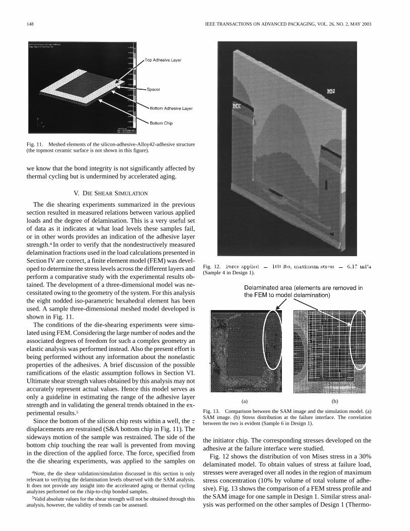
Fig. 11. Meshed elements of the silicon-adhesive-Alloy42-adhesive structure(the topmost ceramic surface is not shown in this figure).
we know that the bond integrity is not significantly affected bythermal cycling but is undermined by accelerated aging.
V. DIE SHEAR SIMULATION
The die shearing experiments summarized in the previoussection resulted in measured relations between various appliedloads and the degree of delamination. This is a very useful setof data as it indicates at what load levels these samples fail,or in other words provides an indication of the adhesive layerstrength.4 In order to verify that the nondestructively measureddelamination fractions used in the load calculations presented inSection IV are correct, a finite element model (FEM) was devel-oped to determine the stress levels across the different layers andperform a comparative study with the experimental results ob-tained. The development of a three-dimensional model was ne-cessitated owing to the geometry of the system. For this analysisthe eight nodded iso-parametric hexahedral element has beenused. A sample three-dimensional meshed model developed isshown in Fig. 11.
The conditions of the die-shearing experiments were simu-lated using FEM. Considering the large number of nodes and theassociated degrees of freedom for such a complex geometry anelastic analysis was performed instead. Also the present effort isbeing performed without any information about the nonelasticproperties of the adhesives. A brief discussion of the possibleramifications of the elastic assumption follows in Section VI.Ultimate shear strength values obtained by this analysis may notaccurately represent actual values. Hence this model serves asonly a guideline in estimating the range of the adhesive layerstrength and in validating the general trends obtained in the ex-perimental results.5
Since the bottom of the silicon chip rests within a well, thedisplacements are restrained (S&A bottom chip in Fig. 11). Thesideways motion of the sample was restrained. The side of thebottom chip touching the rear wall is prevented from movingin the direction of the applied force. The force, specified fromthe die shearing experiments, was applied to the samples on
4Note, the die shear validation/simulation discussed in this section is onlyrelevant to verifying the delamination levels observed with the SAM analysis.It does not provide any insight into the accelerated aging or thermal cyclinganalyzes performed on the chip-to-chip bonded samples.
5Valid absolute values for the shear strength will not be obtained through thisanalysis, however, the validity of trends can be assessed.
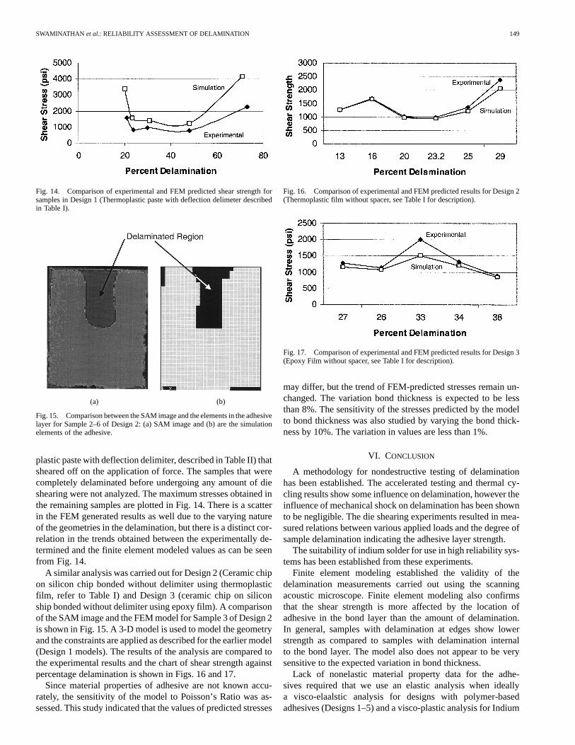
Fig. 12. Force applied = 100 lbs, maximum stress = 6:17 mPa
(Sample 4 in Design 1).
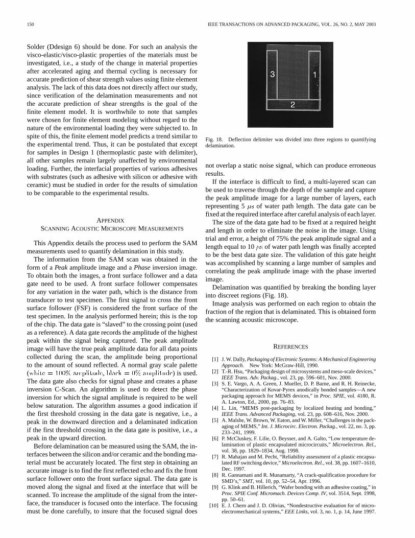
(a) (b)
Fig. 13. Comparison between the SAM image and the simulation model. (a)SAM image. (b) Stress distribution at the failure interface. The correlationbetween the two is evident (Sample 6 in Design 1).
the initiator chip. The corresponding stresses developed on theadhesive at the failure interface were studied.
Fig. 12 shows the distribution of von Mises stress in a 30%delaminated model. To obtain values of stress at failure load,stresses were averaged over all nodes in the region of maximumstress concentration (10% by volume of total volume of adhe-sive). Fig. 13 shows the comparison of a FEM stress profile andthe SAM image for one sample in Design 1. Similar stress anal-ysis was performed on the other samples of Design 1 (Thermo-
SWAMINATHAN et al.: RELIABILITY ASSESSMENT OF DELAMINATION 149
Fig. 14. Comparison of experimental and FEM predicted shear strength forsamples in Design 1 (Thermoplastic paste with deflection delimeter describedin Table I).
(a) (b)
Fig. 15. Comparison between the SAM image and the elements in the adhesivelayer for Sample 2–6 of Design 2: (a) SAM image and (b) are the simulationelements of the adhesive.
plastic paste with deflection delimiter, described in Table II) thatsheared off on the application of force. The samples that werecompletely delaminated before undergoing any amount of dieshearing were not analyzed. The maximum stresses obtained inthe remaining samples are plotted in Fig. 14. There is a scatterin the FEM generated results as well due to the varying natureof the geometries in the delamination, but there is a distinct cor-relation in the trends obtained between the experimentally de-termined and the finite element modeled values as can be seenfrom Fig. 14.
A similar analysis was carried out for Design 2 (Ceramic chipon silicon chip bonded without delimiter using thermoplasticfilm, refer to Table I) and Design 3 (ceramic chip on siliconship bonded without delimiter using epoxy film). A comparisonof the SAM image and the FEM model for Sample 3 of Design 2is shown in Fig. 15. A 3-D model is used to model the geometryand the constraints are applied as described for the earlier model(Design 1 models). The results of the analysis are compared tothe experimental results and the chart of shear strength againstpercentage delamination is shown in Figs. 16 and 17.
Since material properties of adhesive are not known accu-rately, the sensitivity of the model to Poisson’s Ratio was as-sessed. This study indicated that the values of predicted stresses
Fig. 16. Comparison of experimental and FEM predicted results for Design 2(Thermoplastic film without spacer, see Table I for description).
Fig. 17. Comparison of experimental and FEM predicted results for Design 3(Epoxy Film without spacer, see Table I for description).
may differ, but the trend of FEM-predicted stresses remain un-changed. The variation bond thickness is expected to be lessthan 8%. The sensitivity of the stresses predicted by the modelto bond thickness was also studied by varying the bond thick-ness by 10%. The variation in values are less than 1%.
VI. CONCLUSION
A methodology for nondestructive testing of delaminationhas been established. The accelerated testing and thermal cy-cling results show some influence on delamination, however theinfluence of mechanical shock on delamination has been shownto be negligible. The die shearing experiments resulted in mea-sured relations between various applied loads and the degree ofsample delamination indicating the adhesive layer strength.
The suitability of indium solder for use in high reliability sys-tems has been established from these experiments.
Finite element modeling established the validity of thedelamination measurements carried out using the scanningacoustic microscope. Finite element modeling also confirmsthat the shear strength is more affected by the location ofadhesive in the bond layer than the amount of delamination.In general, samples with delamination at edges show lowerstrength as compared to samples with delamination internalto the bond layer. The model also does not appear to be verysensitive to the expected variation in bond thickness.
Lack of nonelastic material property data for the adhe-sives required that we use an elastic analysis when ideallya visco-elaalstic analysis for designs with polymer-basedadhesives (Designs 1–5) and a visco-plastic analysis for Indium
150 IEEE TRANSACTIONS ON ADVANCED PACKAGING, VOL. 26, NO. 2, MAY 2003
Solder (Ddesign 6) should be done. For such an analysis thevisco-elastic/visco-plastic properties of the materials must beinvestigated, i.e., a study of the change in material propertiesafter accelerated aging and thermal cycling is necessary foraccurate prediction of shear strength values using finite elementanalysis. The lack of this data does not directly affect our study,since verification of the delamination measurements and notthe accurate prediction of shear strengths is the goal of thefinite element model. It is worthwhile to note that sampleswere chosen for finite element modeling without regard to thenature of the environmental loading they were subjected to. Inspite of this, the finite element model predicts a trend similar tothe experimental trend. Thus, it can be postulated that exceptfor samples in Design 1 (thermoplastic paste with delimiter),all other samples remain largely unaffected by environmentalloading. Further, the interfacial properties of various adhesiveswith substrates (such as adhesive with silicon or adhesive withceramic) must be studied in order for the results of simulationto be comparable to the experimental results.
APPENDIX
SCANNING ACOUSTICMICROSCOPEMEASUREMENTS
This Appendix details the process used to perform the SAMmeasurements used to quantify delamination in this study.
The information from the SAM scan was obtained in theform of aPeakamplitude image and aPhaseinversion image.To obtain both the images, a front surface follower and a datagate need to be used. A front surface follower compensatesfor any variation in the water path, which is the distance fromtransducer to test specimen. The first signal to cross the frontsurface follower (FSF) is considered the front surface of thetest specimen. In the analysis performed herein; this is the topof the chip. The data gate is “slaved” to the crossing point (usedas a reference). A data gate records the amplitude of the highestpeak within the signal being captured. The peak amplitudeimage will have the true peak amplitude data for all data pointscollected during the scan, the amplitude being proportionalto the amount of sound reflected. A normal gray scale palette( , ) is used.The data gate also checks for signal phase and creates a phaseinversion C-Scan. An algorithm is used to detect the phaseinversion for which the signal amplitude is required to be wellbelow saturation. The algorithm assumes a good indication ifthe first threshold crossing in the data gate is negative, i.e., apeak in the downward direction and a delaminated indicationif the first threshold crossing in the data gate is positive, i.e., apeak in the upward direction.
Before delamination can be measured using the SAM, the in-terfaces between the silicon and/or ceramic and the bonding ma-terial must be accurately located. The first step in obtaining anaccurate image is to find the first reflected echo and fix the frontsurface follower onto the front surface signal. The data gate ismoved along the signal and fixed at the interface that will bescanned. To increase the amplitude of the signal from the inter-face, the transducer is focused onto the interface. The focusingmust be done carefully, to insure that the focused signal does
Fig. 18. Deflection delimiter was divided into three regions to quantifyingdelamination.
not overlap a static noise signal, which can produce erroneousresults.
If the interface is difficult to find, a multi-layered scan canbe used to traverse through the depth of the sample and capturethe peak amplitude image for a large number of layers, eachrepresenting 5 of water path length. The data gate can befixed at the required interface after careful analysis of each layer.
The size of the data gate had to be fixed at a required heightand length in order to eliminate the noise in the image. Usingtrial and error, a height of 75% the peak amplitude signal and alength equal to 10 of water path length was finally acceptedto be the best data gate size. The validation of this gate heightwas accomplished by scanning a large number of samples andcorrelating the peak amplitude image with the phase invertedimage.
Delamination was quantified by breaking the bonding layerinto discreet regions (Fig. 18).
Image analysis was performed on each region to obtain thefraction of the region that is delaminated. This is obtained formthe scanning acoustic microscope.
REFERENCES
[1] J. W. Dally,Packaging of Electronic Systems: A Mechanical EngineeringApproach. New York: McGraw-Hill, 1990.
[2] T.-R. Hsu, “Packaging design of microsystems and meso-scale devices,”IEEE Trans. Adv. Packag., vol. 23, pp. 596–601, Nov. 2000.
[3] S. E. Vargo, A. A. Green, J. Mueller, D. P. Barne, and R. H. Reinecke,“Characterization of Kovar-Pyrex anodically bonded samples—A newpackaging approach for MEMS devices,” inProc. SPIE, vol. 4180, R.A. Lawton, Ed., 2000, pp. 76–83.
[4] L. Lin, “MEMS post-packaging by localized heating and bonding,”IEEE Trans. Advanced Packaging, vol. 23, pp. 608–616, Nov. 2000.
[5] A. Malshe, W. Brown, W. Eaton, and W. Miller, “Challenges in the pack-aging of MEMS,”Int. J. Microcirc. Electron. Packag., vol. 22, no. 3, pp.233–241, 1999.
[6] P. McCluskey, F. Lilie, O. Beysser, and A. Galto, “Low temperature de-lamination of plastic encapsulated microcircuits,”Microelectron. Rel.,vol. 38, pp. 1829–1834, Aug. 1998.
[7] R. Mahajan and M. Pecht, “Reliability assessment of a plastic encapsu-lated RF switching device,”Microelectron. Rel., vol. 38, pp. 1607–1610,Dec. 1997.
[8] R. Gannamani and R. Munamarty, “A crack-qualification procedure forSMD’s,” SMT, vol. 10, pp. 52–54, Apr. 1996.
[9] G. Klink and B. Hillerich, “Wafer bonding with an adhesive coating,” inProc. SPIE Conf. Micromach. Devices Comp. IV, vol. 3514, Sept. 1998,pp. 50–61.
[10] E. J. Chern and J. D. Olivias, “Nondestructive evaluation for of micro-electromechanical systems,”EEE Links, vol. 3, no. 1, p. 14, June 1997.
SWAMINATHAN et al.: RELIABILITY ASSESSMENT OF DELAMINATION 151
[11] A. Herenz, K.-J. Wolter, E. Meusel, B. Hirschfeld, H. Kraytz, and R.Ronniger, “C-SAM evaluation of large bonded areas in the field of mi-cromechanics and microelectronics,” inProc. Int. Acoustic Micro Imag.Symp., Sept. 1999.
[12] L. Fan, H. Last, R. Wood, B. Dudley, C. Khan, C. K. Malek, and Z.Ling, “SLIGA based underwater safety and arming system,”Microsyst.Technol., vol. 4, pp. 168–171, Sept. 1998.
[13] M. Deeds, K. Cochran, P. Sandborn, and R. Swaminathan, “Packagingof a MEMS based safety and arming device,” inProc. Intersoc. Conf.Thermal Phenom. (ITHERM), May 2000, pp. 107–112.
[14] H. Last, M. Deeds, D. Garvick, R. Kavetsky, P. Sandborn, E. B. Magrab,and S. K. Gupta, “Nano-to-millimeter scale integrated systems,”IEEETrans. Comp. Packag. Technol., vol. 22, pp. 338–343, June 1999.
[15] “Cover photographs,”IEEE Trans. Comp. Packag. Technologies, vol.22, pp. 338–343, June 1999.
[16] K. Cochran, L. Fan, and D. L. DeVoe, “High-power optical micro switchfabricated by deep reactive ion etching (DRIE),” inProc. SPIE 4983:MOEMS Min. Syst. III, San Jose, CA, Jan. 2003, pp. 75–86.
[17] Product Data Sheet for Thermoplastic Film (TP 7090), Rev B@03/15/99, Device Push-Off Strength, AI Technology, Princeton, NJ.
Rajesh Swaminathanreceived the B.Tech. degreein chemical engineering from the Indian Institute ofTechnology, Chennai, in 1999 and the M.S. degree inmechanical engineering from the University of Mary-land, College Park, in 2001.
He is currently a Senior Reliability Engineer atBell Labs, Lucent Technologies, Holmdel, NJ. Atthe University of Maryland, his research interestsincluded experimentation, failure mode analysisfor chip-to-chip bonding, carrier level packagingof MEMS systems, and finite element modeling
of packages. At Lucent Technologies, his interests include implementingphysics-of-failure approach to the reliability of fiber optic componentswith emphasis on emerging technologies including MEMS, liquid crystal;sub-micron technologies, RF devices, and thermal analysis of PWBs.
Harish Bhaskaran received the B.E. degree in civilengineering from the College of Engineering, Pune,India, in 2000 and the M.S.degree in mechanical en-gineering from the University of Maryland, CollegePark, in 2002, where he is currently pursuing thePh.D.
His research interests are in the fields of nanotech-nology, MEMS, and electronics packaging. His pre-vious work included experimental and theoretical as-sessment of dominant failure mechanisms in MEMSand optical interfaces to MEMS. His current research
in nanomechanics is focused on novel design and fabrication of ultra-sensitivemechanical resonators for single spin detection with applications on magneticresonance force microscopes.
Peter A. Sandborn(M’87–SM’01) received the B.S.degree in engineering physics from the University ofColorado, Boulder, in 1982, and the M.S. degree inelectrical science and Ph.D. degree in electrical engi-neering from the University of Michigan, Ann Arbor,in 1983 and 1987, respectively.
He is an Associate Professor and the ResearchDirector in the CALCE Electronic Products andSystems Center (EPSC), University of Maryland,College Park, where his interests include technologytradeoff analysis for electronic packaging, system
life cycle economics, and virtual qualification of electronic components andsystems. Prior to joining the University of Maryland, he was a Founder andChief Technical Officer of Savantage, Austin, TX, and a Senior Member ofTechnical Staff, Microelectronics and Computer Technology Corporation,Austin. He is the author of over 80 technical publications and books onmultichip module design and part obsolescence forecasting.
Dr. Sandborn is an Associate Editor of the IEEE TRANSACTIONS ON
ELECTRONICSPACKAGING MANUFACTURING.
Gowrishankar Subramanian received the B.S. de-gree in mechanical engineering from the Indian In-stitute of Technology, Madras, in 1998, and the M.S.degree in mechanical engineering from the Univer-sity of Maryland, College Park, in 2000.
He is a Package Design Engineer at AdvancedMicro Devices, Inc., Sunnyvale, CA, where hisinterests include design and qualification of CSPpackages, qualification of advanced substrate tech-nologies, and board level reliability studies. He isthe author/co-author of four technical publications.
Michael A. Deedsreceived the B.S. and M.S. de-grees in mechanical engineering from the Universityof Maryland, College Park, in 1991 and 1995, respec-tively, where he is currently pursuing the Ph.D. de-gree in mechanical engineering.
He is a Senior Mechanical Engineer in the War-heads Technology and Development Department, In-dian Head Division, Naval Surface Warfare Center,Indian Head, MD. From 1995 until present, he hasserved as a lead Designer on the MEMS Team forFlow Sensing Technology as well as the Lead Engi-
neer for MEMS Packaging. He holds one patent for a MEMS flow sensor thathas been licensed for several fields of use. In addition, he is co-inventor on twoother patent-pending MEMS sensors. He has authored several papers on MEMSpackaging.
Kevin R. Cochran received the B.S. and M.S. de-grees in mechanical engineering from the Universityof Maryland, College Park, in 1998 and 2003, respec-tively.
He is currently employed with the Indian Head Di-vision, Naval Surface Warfare Center, Indian Head,MD, where he is assisting in the development of aMEMS-based safety and arming system for use in un-derwater weapons. His work is focused in the areasof optical MEMS design and MEMS packaging.