Embed Size (px)
Citation preview

IEEE TRANSACTIONS ON ANTENNAS AND PROPAGATION, VOL. 53, NO. 12, DECEMBER 2005 3897
Dual Frequency and Dual Circular PolarizationMicrostrip Nonresonant Array Pin-Fed
From a Radial LineReuven Shavit, Senior Member, IEEE, Lev Pazin, Yaniv Israeli, Michael Sigalov, and Yehuda Leviatan, Fellow, IEEE
Abstract—A new type of a dual frequency and dual circularpolarization multilayer microstrip nonresonant antenna array forsatellite communication is presented. The microstrip radiatingelements in the array are arranged in concentric circles and fedthrough pins embedded in a radial line. The radial line is excitedthrough a probe at its center. The microstrip array exhibits adual frequency band of operation, low side-lobes in the radiationpattern, and high radiation efficiency (more than 65%) for bothpolarizations. The microstrip element has been designed usingcommercial software based on the method of finite integral timedomain algorithm, and the feed network has been designed bya theoretical analysis. A prototype of the array has been builtand tested. The agreement between the measured and numericalresults is satisfactory.
Index Terms—Circular polarization, dual frequency, nonreso-nant microstrip antenna, radial line.
I. INTRODUCTION
THE rapid growth of satellite communication has stimu-lated intensive research concerning medium and high gain
planar antennas. Microstrip nonresonant antennas are consid-ered as an obvious choice for such an application due to theirlow cost, low weight and low profile. However, large microstripantennas for mid and high gain applications encounter a majordeficiency in their performance, due to their high loss experi-enced in the feed network. These losses reduce the achievableradiation efficiency to less than 40%. A possible solution to thisproblem is to replace the standard microstrip feed network witha radial line (radial waveguide) feed network. A radial line feednetwork is subject to much lower losses. Hence, it is an attractivealternative. This type of network was first conceptualized andbuilt by Goebels and Kelly [1] to feed a flat antenna with annularslots as radiators, also called radial line slot antenna (RLSA). Aderivative from RLSA concept was studied by Carver [2] andNakano [3], in which the radiating elements in the array are he-lices fed from a radial line through small wire pins to obtaincircular polarization. The radial line was excited at its center bya probe and the helices were distributed circularly on the top sur-face of the radial line on concentric circles. In 1991, Haneishi
Manuscript received February 14, 2005; revised August 21, 2005. Thisproject was supported by ISIS consortium, Trade and Industry Ministry, Israel.
R. Shavit and M. Sigalov are with the Department of Electrical and ComputerEngineering, Ben-Gurion University of the Negev, Beer Sheva 84105, Israel.
Y. Israeli is with the Antenna Department, Elta Systems Group Ltd., Ashdod77102, Israel.
L. Pazin and Y. Leviatan are with the Department of Electrical Engineering,Technion – Israel Institute of Technology, Haifa 32000, Israel.
Digital Object Identifier 10.1109/TAP.2005.859911
et al. [4] replaced the helices with circular polarized microstripelements to obtain a high efficiency (90%) antenna in Ku band.These elements were used also by Yamamoto et al. [5] to designa circular array antenna with shaped beam. In the circular polar-ization antennas described in [2]–[5], the arrays are nonresonantand uniformly excited. Hence, the outer circle of radiating ele-ments in these arrays is strongly coupled to the waveguide andserves also as an effective termination (load of the waveguide).Other types of the radial line planar microstrip array antennasare described in [6], [7].
In this paper, a new type Ku band, dual frequency and dual cir-cular polarization multilayer microstrip array antenna with lowside-lobes fed from a radial line through wire pins is presented.The motivation is the design of a two-way terminal antenna forlow earth orbit (LEO) satellite communication from a mobileplatform. The radiating element is composed from two stackedcircular patches fed by a single feeding pin. The circular polar-ization is achieved for each circular patch by introducing twoindents as described in [8]. The uniqueness of the proposed el-ement is that it enables to control independently the radiatedphase of each of the patches by turning the two patches aroundtheir common feeding point. The computation of the radiationparameters of the radiating element was conducted using theMWS commercial software from CST, which is based on a fi-nite integral time domain (FITD) algorithm. The radiating ele-ments are distributed on concentric circles and the radial line isfed through a wire probe at its center. The lengths and couplingto the wire pins inserted in the radial line have been determinedthrough an analytical procedure outlined in [9], [10]. A proto-type of an array with 8 rings operating in two frequency ranges11.7–12.2 GHz (low frequency band) with right hand circularpolarization (RHCP) and 14–14.5 GHz (high frequency band)with left hand circular polarization (LHCP) has been built andtested. The agreement between the computed and the test resultsis satisfactory.
II. THE RADIATING ELEMENT
The basic structure of the proposed element operating in twoKu frequency bands and two orthogonal circular polarizationsis shown in Fig. 1. Two stacked circular patches are fed intandem by a single pin. Each patch is coupled eccentrically tothe feeding pin through an annular gap [11], [12]. This uniquetype of feeding is necessary in order to introduce a capacitiveeffect to counterbalance the inductive effect of the feeding pin.The feeding pin is top loaded with a little circular pad as an
0018-926X/$20.00 © 2005 IEEE

3898 IEEE TRANSACTIONS ON ANTENNAS AND PROPAGATION, VOL. 53, NO. 12, DECEMBER 2005
Fig. 1. Geometry of the dual frequency, dual circular polarization microstripantenna: (a) cross section and (b) top view.
additional matching element. The upper patch “ground plane”is the lower patch. To ensure a large enough “ground plane”for the upper patch in all of its turning angular positions [forexample, in positions A and B shown in Fig. 1(b)], the diameterof the upper patch (operating in the upper frequency band) mustbe considerably less than that of the lower patch (operating inthe lower frequency band). This may be achieved by choosingthe relative permittivity of the substrate between the lowerpatch and the ground plane to be close to unity, and, on contrary,by choice of considerably greater relative permittivity of thesubstrate between the two patches.
In the design of the proposed element the lowest layer is Ro-hacell foam with electrical properties 1.067,0.0041 and thickness 0.761 mm. The substrate between the twopatches is Rogers RO3006 with electrical properties 6.15,
0.002 and thickness 0.64 mm. To reduce mutual cou-pling among the elements in the array through surface wavescoupling, this layer was truncated to a square 12 mm 12 mm asshown in Fig. 1. The truncation has a minimal effect on the radi-ation characteristics of the element. The top pad is printed on theRogers substrate RO4350 with electrical properties 3.48,
0.001 and thickness 0.1 mm.A parametric study to optimize the element performance was
conducted. For the operating frequencies 11.95 GHz (RHCP,lower patch) and 14.25 GHz (LHCP, upper patch), the patch di-ameters found are 9.14 and 4.24 mm, respectively, and the diam-eters of the annular gaps are 0.9 mm (inner) and 1.3 mm (outer).The eccentricity of the feeding pin position is chosen by [11] as1.75 mm for the lower patch and 0.9 mm for the upper patch,to match the radiation element 50 Ohm input impedance of asimple, nonstacked circular patch. As a result, in the considered
Fig. 2. Effect of the upper patch turning on the electrical phase of the radiatedfield: (a) lower and upper patch layouts for turning angles ' = 0 (to the left)and ' = 120 (to the right) and (b) dependence of the electrical phase on theturning angle of the upper patch at 14.25 GHz.
stacked element, the values of the patch turning angles vary fromcircle to circle and correspondingly its dimensions, spacing be-tween adjacent elements, mutual coupling and input impedancesare changed. The corresponding optimum pad diameter is 1.3mm. The diameter of the feeding pin is equal to 0.3 mm and thediameter of the pin together with the soldered metalized layer inthe substrate package is equal to 0.7 mm. The entire multilayerstructure is bonded with adhesive films. The choice of the filmshas been made based on practical considerations and availableadhesive films with electrical properties as close as possible tothe corresponding substrate. The adhesive film used to bond theRO4350 substrate to the RO3006 substrate is of thickness 0.1mm and electrical properties 3.17, 0.005, whileon both sides of the foam the adhesive films used are of thick-ness 0.03 mm and electrical properties 5, 0.005.The indent dimensions in the circular patches to generate cir-cular polarization [8] are 0.84 mm 0.42 mm for the upperpatch and 1.6 mm 0.8 mm for the lower patch.
The dependence of the radiated electrical field phase on thephysical turning angle of the lower patch around the feedingpoint was tested and found to be linear as expected. To inves-tigate the dependence of the radiated electrical phase variationwith the upper patch turning, ten more element prototypes withthe upper patch turned around the feeding point (lower patchremaining fixed) in steps of 30 have been fabricated and mea-sured. Fig. 2 shows the effect of the upper patch turning. InFig. 2(a) one can observe lower and upper patch layouts forcounter-clockwise (CCW) turning angles 0 (to the left)and 120 (to the right). Here, O designates the location ofthe feeding pin, and and denote, respectively, the cen-ters of the lower and upper patches. Fig. 2(b) shows the depen-dence of the measured radiated electrical field phase at 14.25

SHAVIT et al.: DUAL FREQUENCY AND DUAL CIRCULAR POLARIZATION MICROSTRIP NONRESONANT ARRAY PIN-FED FROM A RADIAL LINE 3899
Fig. 3. Radiating element typical input impedance: (a) low frequency band and (b) high frequency band.
Fig. 4. Radiating element axial ratio versus frequency: (a) low frequency band and (b) high frequency band.
GHz on the turning angle of the upper patch around the feedingpoint with the lower patch fixed. In a perfect scenario, it is ex-pected that a linear dependence would exist between the phaseand the turning angle. As one can notice, the dependence of themeasured phase is not perfectly linear due to the inherent asym-metric nature of the structure (the upper patch vis-à-vis the lowerpatch). This phase variation has been taken in consideration inthe array design.
Fig. 3 shows the typical computed and measured inputimpedance of the stand-alone stacked radiating element. Onecan observe that the calculated and measured results are insatisfactory agreement. In the feed network design, we usedmeasured values for the input impedances of the radiatingelements in each circle. Fig. 4 shows the element axial ratiodependence on frequency. It can be noticed that the measuredradiating element axial ratio is 1.4 dB at 12.05 GHz and 2.3dB at 14.2 GHz. In the high frequency band the agreementbetween measured and computed values is good. A slight shiftcan be noticed in the minimum axial ratio location in the lowerfrequency band, with 12.05 GHz measured value and 11.9 GHz
computed value. This shift can be attributed to the multilayerelement fabrication process in which some particles of theadhesive film penetrates into the Rohacell foam and changesits electrical properties.
III. FEED NETWORK DESIGN
A picture of the antenna prototype fabricated and its feed net-work are shown in Fig. 5. The array elements are truncated to asquare shape 12 mm 12 mm. The truncated element structurecontains the two circular patches shown in Fig. 1. The heightof the radial line is 7.5 mm, close to quarter-wavelength.A traveling cylindrical TEM mode is generated by the centralfeeding probe and is propagating along the radial line as a trav-eling wave weakly coupled to the wire pins of the radiating ele-ments. To avoid reflection from the radial line rim, the residual,nonradiated power (22% at 11.95 GHz and 8% at 14.25 GHz) isabsorbed in a matched termination load. The termination loadis a one-wavelength wide strip of dielectric flexible absorbingmaterial ARC-LS-10 211 cut in a saw-tooth pattern [termination

3900 IEEE TRANSACTIONS ON ANTENNAS AND PROPAGATION, VOL. 53, NO. 12, DECEMBER 2005
Fig. 5. Microstrip antenna array: (a) top view picture of the prototype and (b) schematic cross section of the feed network.
load is shown schematically in Fig. 5(b)]. To avoid the gratinglobes in the radiation pattern, the feeding wire pins of the radi-ating elements are distributed on concentric circles with radialspacing 17.5 mm (0.7 at 12 GHz and 0.83 at 14.2GHz). To obtain a uniform element distribution on the aperture
, it can be shown by [4], the optimal number of ra-diating elements on each circle should satisfy the condition
6 1 2 . For practical reasons, the number ofcircles in this project was selected to be 8 (total number ofelements in the array is 216). The spacing between adjacent pinson each circle is 18.3 mm (0.73 at 12 GHz and 0.86at 14.2 GHz). To improve the antenna input matching over theentire frequency band, the central probe was wrapped with a di-electric sleeve as shown in Fig. 5(b).
Initial uniform phase distribution on the array aperture (ne-glecting external mutual coupling between radiating elements)can be achieved only for one frequency in each frequency range.This feature is accomplished by turning the upper and lower ra-diating patch elements independently to offset the variation inthe electrical phase delay between adjacent circles in the radialline. The turning angles have been calculated by [9] for the cen-tral frequencies of each frequency band.
The crucial part of the design scheme is the determinationof the pin lengths required to achieve the desired excitationcoefficients . To obtain a low side-lobe level in the radiationpatterns, an initial bell-shaped amplitude distribution (BSAD)with a taper parameter of 0.7 has been chosen [9]. Theexcitation coefficients in this case are given by
1 0.35 1 (1)
and presented for 8 in Table I. The required couplingcoefficient, which determines the power delivered by the feedsystem to the radiating elements, is given in decibels by
10 (2)
where is a termination parameter (a ratio between the powerabsorbed in the termination load and the total power radiatedby all elements of the outer circle [9]). Calculated results of
, for 3, are presented in Table I. As shown in [10],this coupling coefficient can also be written in terms of the feednetwork parameters as
101.5
(3)
where is the radiating element input resistance, and isthe input impedance of the loaded pin in the array [10]. Now,requiring that be equal to , we can derive the pin length
needed to attain the desired array amplitude distribution.This procedure takes in consideration the internal mutual cou-
pling among the pins, the loading of the all radiating elements,the waveguide termination, and the transforming properties ofthe coaxial channels in the radial waveguide cover. Based on thecomputed coupling coefficients, the required pin lengths for allcircles in the array were determined and averaged (see Table I).
One can observe that for the initial BSAD, the variation inthe calculated wire pin length is negligible for some circles ofthe array. This result triggered the idea to divide the radial line

SHAVIT et al.: DUAL FREQUENCY AND DUAL CIRCULAR POLARIZATION MICROSTRIP NONRESONANT ARRAY PIN-FED FROM A RADIAL LINE 3901
TABLE IINITIAL VALUES AND FINAL CALCULATED RESULTS OF THE PIN LENGTH AND AVERAGE AMPLITUDE DISTRIBUTIONS ON THE ANTENNA FEED NETWORK
in several sections, such that in each section the coupling pinlengths will be kept constant in spite of some distortion ofthe initial amplitude distribution. Furthermore, to improve theaccuracy of the fabrication process, it was realized that it wouldbe more beneficial if the tips of all pins will end at the same zposition. Finally, the radial line was manufactured from threesections with compensated jump discontinuities at the interfacebetween adjacent sections as shown in Fig. 5(b) (radial line crosssection), while the total pin lengths (each pin consists of the cou-pling pin length, the segment in the radiating elements, and thesegment in the coaxial channel in the radial waveguide cover)are kept constant and equal to 12 mm. The first section consistsof the first circle 3.3 mm , the second section consists ofsecond and third circles 3.8 mm and the third sec-tion consists of the rest of circles 4.3 mm .It should be noted that while the calculated values of the pinlengths of the elements on the fourth circle imply that this circleshould have been in the second section of the waveguide, itwas nevertheless placed in the third section of the waveguide.This arrangement was made to compensate the error made inthe other pin lengths and particularly render the aperture ampli-tude distribution at the higher operating frequency more close tothe desired bell-shaped one. Table I also presents the final calcu-lated average coupling coefficients and amplitude distribu-tion with the above pin lengths to obtain the reduced side-lobelevel radiation pattern in both frequency bands. Fig. 6 showsgraphically the dependence of the calculated pins coupling co-efficients on different circles in the array for the final calculatedamplitude distribution.
To assess the magnitude of the external mutual couplingbetween the array elements, an investigation has been launchedto determine its value. Fig. 7 shows the mutual coupling value
of a typical element on the second circle to its closestneighbors. One can observe, as expected that the highest mutualcoupling is obtained from the closest neighbors on the third andfirst circles. The maximum value of in the low frequencyband it is 20 dB, while in the upper frequency band themaximum value it is 18 dB, which corresponds to knownresults [13]. The external mutual coupling effect on the antenna
Fig. 6. Coupling coefficient dependence on different circles in the array.
amplitude and phase aperture distributions is random due to thefact that the centers of the radiating elements and their feedingpoints do not coincide. This introduces also randomness inthe distribution of the array elements centers, which reducesthe mutual coupling effect. To further reduce the effect ofthis mutual coupling, it was found experimentally that, forlarge spacing 0.8 , the pins of the first circle must beshifted by 15 in the azimuthal direction relative to the pinsof the second circle (see Fig. 5(a), where the pin positionsare shown as dots on the radiating element surfaces). Thisreduces the frequency-dependent periodic fluctuations of themutual coupling along the second circle. In the suggested shiftedposition, all elements of the second circle are equally allocatedrelative to the pins of the first circle and ensure that all theelements in each of the two circles are equally excited.
IV. EXPERIMENTAL RESULTS
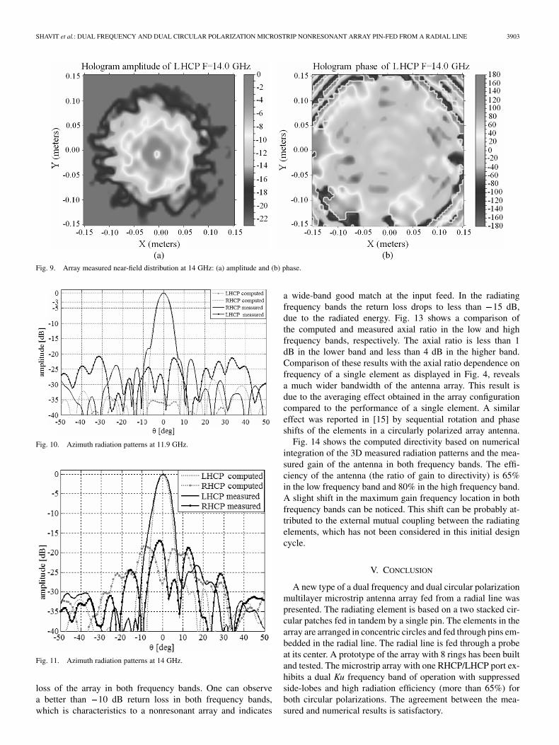
The antenna performance has been tested on a prototype 30cm in diameter with eight circles 17.5 mm spaced. Figs. 8 and 9show the measured near-field distribution (amplitude and phase)at the frequencies 11.9 and 14 GHz. One can observe that at 11.9

3902 IEEE TRANSACTIONS ON ANTENNAS AND PROPAGATION, VOL. 53, NO. 12, DECEMBER 2005
Fig. 7. Return loss and external mutual coupling coefficients for a typical element on the second circle in the array.
Fig. 8. Array measured near-field distribution at 11.9 GHz: (a) amplitude and (b) phase.
GHz both amplitude and phase distributions exhibit a spiral pat-tern instead of a ring pattern as expected. Such a distribution canbe explained by the nonuniform mutual coupling effect betweenradiating elements in the array. In the array, the phases of theradiating elements are obtained by locating the pins of the radi-ating elements on radially equispaced circles and by additionalturning of each element around its feeding pin. This elementrotation is eccentric and cause nonuniform spacing between el-ements edges on different circles. Accordingly, the mutual cou-pling effect between elements on different circles is unequal andperturbs the aperture distribution to a spiral shape instead of aconstant circle distribution as desired. At 14 GHz, one can ob-serve a “hexagonal” near-field aperture distribution. Compar-ison of the measured amplitude distributions in Figs. 8(a) and9(a) reveals higher tapering at 14 GHz. Results represented inFigs. 8(b) and 9(b) show that the maximum phase deviation inthe aperture is approximately 6. Based on [14], such
phase error can lead to some reduction in the gain, though notmore than 1.3 dB.
Figs. 10 and 11 show a comparison of computed and measuredcopol and cross-pol azimuth patterns at 11.9 and 14 GHz,respectively.Thecomputedradiationpatternshavebeenobtainedbased on the simulated complex fields of the radiating elementson different circles, the final relative amplitude excitationsdescribed in Table I taking in consideration the position of eachpin in the array, and the electrical phase delay between adjacentcircles in the radial line.Onecanobserveasatisfactoryagreementbetween the computed and measured radiation patterns. Thepatterns at both frequencies exhibit a reduced sidelobe level(less than 20 dB). The cross-pol sidelobe level at 11.9 GHzis lower than the sidelobe level at 14 GHz. The main reasonfor the difference can be attributed to the nonsymmetric natureof the radiating element at the low and high frequency bandsas discussed in Section II. Fig. 12 shows the measured return
SHAVIT et al.: DUAL FREQUENCY AND DUAL CIRCULAR POLARIZATION MICROSTRIP NONRESONANT ARRAY PIN-FED FROM A RADIAL LINE 3903
Fig. 9. Array measured near-field distribution at 14 GHz: (a) amplitude and (b) phase.
Fig. 10. Azimuth radiation patterns at 11.9 GHz.
Fig. 11. Azimuth radiation patterns at 14 GHz.
loss of the array in both frequency bands. One can observea better than 10 dB return loss in both frequency bands,which is characteristics to a nonresonant array and indicates
a wide-band good match at the input feed. In the radiatingfrequency bands the return loss drops to less than 15 dB,due to the radiated energy. Fig. 13 shows a comparison ofthe computed and measured axial ratio in the low and highfrequency bands, respectively. The axial ratio is less than 1dB in the lower band and less than 4 dB in the higher band.Comparison of these results with the axial ratio dependence onfrequency of a single element as displayed in Fig. 4, revealsa much wider bandwidth of the antenna array. This result isdue to the averaging effect obtained in the array configurationcompared to the performance of a single element. A similareffect was reported in [15] by sequential rotation and phaseshifts of the elements in a circularly polarized array antenna.
Fig. 14 shows the computed directivity based on numericalintegration of the 3D measured radiation patterns and the mea-sured gain of the antenna in both frequency bands. The effi-ciency of the antenna (the ratio of gain to directivity) is 65%in the low frequency band and 80% in the high frequency band.A slight shift in the maximum gain frequency location in bothfrequency bands can be noticed. This shift can be probably at-tributed to the external mutual coupling between the radiatingelements, which has not been considered in this initial designcycle.
V. CONCLUSION
A new type of a dual frequency and dual circular polarizationmultilayer microstrip antenna array fed from a radial line waspresented. The radiating element is based on a two stacked cir-cular patches fed in tandem by a single pin. The elements in thearray are arranged in concentric circles and fed through pins em-bedded in the radial line. The radial line is fed through a probeat its center. A prototype of the array with 8 rings has been builtand tested. The microstrip array with one RHCP/LHCP port ex-hibits a dual Ku frequency band of operation with suppressedside-lobes and high radiation efficiency (more than 65%) forboth circular polarizations. The agreement between the mea-sured and numerical results is satisfactory.

3904 IEEE TRANSACTIONS ON ANTENNAS AND PROPAGATION, VOL. 53, NO. 12, DECEMBER 2005
Fig. 12. Measured array return loss versus frequency: (a) low frequency band and (b) high frequency band.
Fig. 13. Axial ratio versus frequency: (a) low frequency band and (b) high frequency band.
Fig. 14. Gain and directivity versus frequency: (a) low frequency band and (b) high frequency band.
ACKNOWLEDGMENT
The authors would like to express their appreciation to PCB,M. Haemek, Israel and especially to Mr. I. Reef for fabricationof the antenna prototype.
REFERENCES
[1] F. J. Goebels and K. C. Kelly, “Arbitrary polarization from annular slotplanar antennas,” IRE Trans. Antennas Propag., vol. 4, pp. 342–349, Jul.1961.
[2] K. R. Carver, “A Cavity-fed concentric ring phased array of helices foruse in radio astronomy,” Ph.D dissertation, Ohio State Univ., 1967.
[3] H. Nakano, H. Takeda, Y. Kitamura, H. Mimaki, and J. Yamauchi, “Low-profile helical array antenna fed from a radial waveguide,” IEEE Trans.Antennas Propag., vol. 3, pp. 279–284, Mar. 1992.
[4] M. Haneishi and S. Saito, “Radiation properties of microstrip array an-tenna fed by radial line,” in IEEE AP Symp. Dig., 1991, pp. 588–591.
[5] N. Yamamoto, S. Saito, S. Morishita, and M. Haneishi, “Radiation prop-erties of shaped beam antenna using radial line microstrip array,” in IEEEAP Symp. Dig., 1996, pp. 1924–1927.
[6] H. Miyashita and T. Katagi, “Radial line planar monopulse antenna,”IEEE Trans. Antennas Propag., vol. 8, pp. 1158–1165, Aug. 1996.

SHAVIT et al.: DUAL FREQUENCY AND DUAL CIRCULAR POLARIZATION MICROSTRIP NONRESONANT ARRAY PIN-FED FROM A RADIAL LINE 3905
[7] K. M. Luk, L. K. Au Yeung, and K. F. Lee, “A broadband linearly polar-ized microstrip antenna array,” in Proc. Asia-Pacific Microwave Conf.,IEICE, 1998, pp. 1039–1041.
[8] M. Haneishi, T. Nambara, and S. Yoshida, “Study on ellipticity proper-ties of single-feed-type circularly polarized microstrip antennas,” Elec-tron. Lett., vol. 18, pp. 191–193, 1982.
[9] L. Pazin and Y. Leviatan, “Effect of amplitude tapering and frequency-dependent phase errors on radiating characteristics of radial waveguidefed nonresonant array antenna,” Proc. Inst. Elect. Eng. Microw. AntennasPropag., vol. 151, no. 4, pp. 363–369, Aug. 2004.
[10] , “Uniform amplitude excitation of radiating elements in array an-tenna pin-fed from radial waveguide,” IProc. Inst. Elect. Eng. Microw.Antennas Propag., vol. 148, no. 6, pp. 413–417, Dec. 2001.
[11] S. A. Long, L. C. Shen, M. D. Walton, and M. R. Allerding, “Impedanceof a circular-disc printed circuit antenna,” Elect. Lett., vol. 14, pp.684–686, 1978.
[12] P. S. Hall, “Probe compensation in thick microstrip patches,” Elect. Lett.,vol. 23, pp. 606–607, 1987.
[13] J. R. James and R. S. Hall, Handbook of Microstrip Antennas. Oxford,U.K.: Peter Peregrinus, 1989, vol. 1, p. 252.
[14] D. K. Cheng, “Effect of arbitrary phase errors on gain and beamwidthcharacteristics of radiation pattern,” IRE Trans. Antennas Propag., vol.AP-3, pp. 145–147, Jul. 1955.
[15] T. Teshirogi, M. Tanaka, and W. Chujo, “Wideband circularly polarizedarray antenna with sequential rotation and phase shifts of elements,”in Proc. Int. Symp. Antennas Propag., vol. 1, Japan, Aug. 1985, pp.117–120.
Reuven Shavit (M’82–SM’90) was born in Ro-mania on November 14, 1949. He received the B.S.and M.S. degrees in electrical engineering from theTechnion – Israel Institute of Technology, Haifa,Israel, in 1971 and 1977, respectively, and the Ph.D.degree in electrical engineering from the Universityof California, Los Angeles, in 1982.
From 1971 to 1993, he worked as a Staff Engi-neer and Antenna Group Leader in the ElectronicResearch Laboratories of the Israeli Ministry ofDefense, Tel Aviv, where he was involved in the
design of reflector, microstrip, and slot antenna arrays. He was also a part-timeLecturer at Tel Aviv University, teaching various antenna and electromagneticcourses. From 1988 to 1990, he was associated with ESSCO, Concord, MA,as a Principal Engineer involved in scattering analysis and tuning techniquesof high performance ground based radomes. Currently, he is with Ben-GurionUniversity of the Negev, Beer-Sheva, Israel, as an Associate Professor doingresearch in microwave components and antennas. His present research interestis in the areas of tuning techniques for radomes and numerical methods fordesign microstrip, slot and reflector antennas.
Lev Pazin was born in Belarus on May 28, 1932.He received the M.Sc. degree in radio mechanicsfrom the Institute of Fine Mechanics and Optics,Leningrad, U.S.S.R. (now St. Petersburg, Russia),in 1955, and the Ph.D. degree in radio location andradio navigation from the Scientific and ResearchInstitute Mars, Leningrad, U.S.S.R., in 1973.
From 1955 to 1957, he was an Engineer with theAssociation Ravenstvo. From 1957 to 1998, he waswith the Holding Company Leninets in Leningrad,serving as Senior Engineer, Leading Engineer, Senior
Scientist, and a Chief of the Laboratory. In 1994, he was awarded an academictitle of Senior Research Scientist. Since 2000, he has been with the Departmentof Electrical Engineering, Technion – Israel Institute of Technology, Haifa, Is-rael, working as a Research Scientist. He has authored and coauthored 17 in-ventions and more than 40 journal and conference papers and reports. His mainscientific and research interests include array antenna feed networks, near andradiated fields of aperture antennas, and controlled waveguide devices.
Yaniv Israeli was born in Tel-Aviv, Israel in 1974.He received the B.Sc. degree in electrical and com-puter engineering from Ben-Gurion University of theNegev, Beer-Sheva, Israel, in 2000.
In 2000, he joined the Antenna Department, EltaSystems Group Ltd., Ashdod, Israel, as a Staff Engi-neer.
Michael Sigalov was born in Erevan, Armenia, in1972. He received the B.Sc. and M.Sc. degrees inelectrical and computer engineering from the Ben-Gurion University of the Negev, Beer-Sheva, Israel,in 2001 and 2005, respectively. Since 2004, he hasbeen working toward the Ph.D. degree at the sameuniversity.
His research interests include quantum confine-ment magnetic-dipolar oscillation in ferrite disks,bianisotropic meta-materials, microwave microscopyand antennas.
Yehuda Leviatan (S’81–M’81–SM’88–F’98) wasborn in Jerusalem, Israel, on September 19, 1951.He received the B.Sc. and M.Sc. degrees in electricalengineering from the Technion—Israel Institute ofTechnology, Haifa, Israel, in 1977 and 1979, respec-tively, and the Ph.D. degree in electrical engineeringfrom Syracuse University, Syracuse, NY, in 1982.
He spent the 1982/1983 academic year as anAssistant Professor at Syracuse University andsubsequently joined the Department of ElectricalEngineering at the Technion – Israel Institute of
Technology, where at present he is a Professor and the incumbent of theJoseph and Sadie Riesman Chair in Electrical Engineering. During his tenureat the Technion he held short-term visiting positions at Cornell University, theSwiss Federal Institute of Technology (ETH), Zurich, the Catholic Universityof America, the University d’Aix-Marseilles III, the University of IllinoisUrbana-Champaign, the University of Washington, Bell Laboratories, andthe University of Michigan. During 1989 to 1991, while on sabbatical leavefrom the Technion, he was with the Department of Electrical Engineeringand Computer Science, The George Washington University, Washington, as aDistinguished Visiting Professor. He is a world-renowned authority in the fieldof computational electromagnetics. He has published more than 90 journalpapers and presented many others at international symposia.
Prof. Leviatan is a Member of Commission B of the International Union ofRadio Science (URSI). He was a recipient of the 2001 Henry Taub Prize forExcellence in Research.


![Elastic helices Comprehensive exam reportpub.bojand.org/ehelices.pdfStability Certain instabilities of helices have been well studied, including su-percoiling [11] and the perversion](https://img.pdfslide.net/doc/110x75/60bc33c276ebf805a23cb455/elastic-helices-comprehensive-exam-stability-certain-instabilities-of-helices-have.jpg)


![The packing of [alpha]-helices: simple coiled-coils](https://img.pdfslide.net/doc/110x75/61fb83342e268c58cd5f0cd4/the-packing-of-alpha-helices-simple-coiled-coils.jpg)