Embed Size (px)
Citation preview
©2018 IEEE. Personal use of this material is permitted. Permission from IEEE must be obtained for all other uses, including reprinting/republishingthis material for advertising or promotional purposes, collecting new collected works for resale or redistribution to servers or lists, or reuse of anycopyrighted component of this work in other works.This document is the paper as accepted for publication in TBioCAS, the fully-edited paper is available at https://ieeexplore.ieee.org/document/8528875.DOI: 10.1109/TBCAS.2018.2880425
IEEE TRANSACTIONS ON BIOMEDICAL CIRCUITS AND SYSTEMS, VOL. XX, NO. XX, XXXXX 2018 1
A 0.086-mm2 12.7-pJ/SOP 64k-Synapse256-Neuron Online-Learning Digital Spiking
Neuromorphic Processor in 28nm CMOSCharlotte Frenkel, Student Member, IEEE, Martin Lefebvre, Student Member, IEEE,
Jean-Didier Legat, Senior Member, IEEE, and David Bol, Senior Member, IEEE
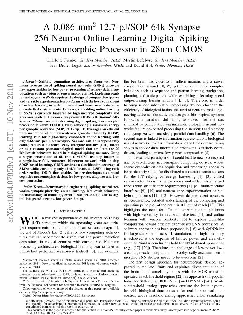
Abstract—Shifting computing architectures from von Neu-mann to event-based spiking neural networks (SNNs) uncoversnew opportunities for low-power processing of sensory data in ap-plications such as vision or sensorimotor control. Exploring roadstoward cognitive SNNs requires the design of compact, low-powerand versatile experimentation platforms with the key requirementof online learning in order to adapt and learn new features inuncontrolled environments. However, embedding online learningin SNNs is currently hindered by high incurred complexity andarea overheads. In this work, we present ODIN, a 0.086-mm2 64k-synapse 256-neuron online-learning digital spiking neuromorphicprocessor in 28nm FDSOI CMOS achieving a minimum energyper synaptic operation (SOP) of 12.7pJ. It leverages an efficientimplementation of the spike-driven synaptic plasticity (SDSP)learning rule for high-density embedded online learning withonly 0.68µm2 per 4-bit synapse. Neurons can be independentlyconfigured as a standard leaky integrate-and-fire (LIF) modelor as a custom phenomenological model that emulates the 20Izhikevich behaviors found in biological spiking neurons. Usinga single presentation of 6k 16×16 MNIST training images toa single-layer fully-connected 10-neuron network with on-chipSDSP-based learning, ODIN achieves a classification accuracy of84.5% while consuming only 15nJ/inference at 0.55V using rankorder coding. ODIN thus enables further developments towardcognitive neuromorphic devices for low-power, adaptive and low-cost processing.
Index Terms—Neuromorphic engineering, spiking neural net-works, synaptic plasticity, online learning, Izhikevich behaviors,phenomenological modeling, event-based processing, CMOS dig-ital integrated circuits, low-power design.
I. INTRODUCTION
WHILE a massive deployment of the Internet-of-Things(IoT) paradigm within the upcoming years sets strin-
gent requirements for autonomous smart sensors design [1],the end of Moore’s law [2] calls for new computing architec-tures that can accommodate severe cost and power reductionconstraints. In radical contrast with current von Neumannprocessing architectures, biological brains appear to have anunmatched performance-resource tradeoff [3]: for example,
Manuscript received xxxxx xx, 2018; revised xxxxx xx, 2018; acceptedxxxxx xx, 2018. Date of publication xxxxx xx, 2018; date of current versionxxxxx xx, 2018.
The authors are with the ICTEAM Institute, Universite catholique deLouvain, Louvain-la-Neuve BE-1348, Belgium (e-mail: {charlotte.frenkel,martin.lefebvre, jean-didier.legat, david.bol}@uclouvain.be).
C. Frenkel is with Universite catholique de Louvain as a Research Fellowfrom the National Foundation for Scientific Research (FNRS) of Belgium.
Color versions of one or more of the figures in this paper are availableonline at http://ieeexplore.ieee.org.
Digital Object Identifier xx.xxxx/TBCAS.2018.xxxxxxx
the bee brain has close to 1 million neurons and a powerconsumption around 10µW, yet it is capable of complexbehaviors such as sequence and pattern learning, navigation,planning and anticipation, while exhibiting a learning speedoutperforming human infants [4], [5]. Therefore, in orderto bring silicon information processing devices closer to theefficiency of biological brains, the field of neuromorphic engi-neering addresses the study and design of bio-inspired systemsfollowing a paradigm shift along two axes. The first axisis linked to computation organization: biological neural net-works feature co-located processing (i.e. neurons) and memory(i.e. synapses) with massively-parallel data handling [6]. Thesecond axis is linked to information representation: biologicalneural networks process information in the time domain, usingspikes to encode data. Information processing is entirely event-driven, leading to sparse low-power computation [5].
This two-fold paradigm shift could lead to new bio-inspiredand power-efficient neuromorphic computing devices, whosesparse event-driven data acquisition and processing appear tobe particularly suited for distributed autonomous smart sensorsfor the IoT relying on energy harvesting [1], [3], closedsensorimotor loops for autonomous embedded systems androbots with strict battery requirements [7], [8], brain-machineinterfaces [9], [10] and neuroscience experimentation or bio-hybrid platforms [11], [12]. However, despite recent advancesin neuroscience, detailed understanding of the computing andoperating principles of the brain is still out of reach [13]. Thishighlights the need for efficient experimentation platformswith high versatility in neuronal behaviors [14] and onlinelearning with synaptic plasticity [15] to explore brain-likecomputation toward efficient event-based SNN processors. Asoftware approach has been proposed in [16] with SpiNNakerfor large-scale neural network simulation, but high flexibilityis achieved at the expense of limited power and area effi-ciencies. Similar conclusions hold for FPGA-based approaches(e.g., [17]–[20]). Therefore, the challenge of low-power low-area large-scale integration of biophysically-accurate neuro-morphic SNN devices needs to be overcome [21].
The first design approach for neuromorphic devices ap-peared in the late 1980s and exploited direct emulation ofthe brain ion channels dynamics with the MOS transistoroperated in subthreshold regime [22], an approach still populartoday for SNNs (e.g., ROLLS [23] and DYNAPs [24]). Whilesubthreshold analog approaches emulate the brain dynam-ics with biological time constant for real-time sensorimotorcontrol, above-threshold analog approaches allow simulating
arX
iv:1
804.
0785
8v3
[cs
.ET
] 1
0 N
ov 2
018
2 IEEE TRANSACTIONS ON BIOMEDICAL CIRCUITS AND SYSTEMS, VOL. XX, NO. XX, XXXXX 2018
neurons with acceleration factors of up to 100,000 for fast pro-cessing (e.g., BrainScaleS [25]). A switched-capacitor analogimplementation has also been proposed to ease robust analogdesign in deep submicron technologies [26], [27]. However,in order to fully leverage technology scaling, several researchgroups recently started designing digital SNNs (e.g., Seo et al.in [28], Kim et al. in [29], IBM with TrueNorth [30] and Intelwith Loihi [31]). Digital designs have a shorter design cycle,low sensitivity to noise, process-voltage-temperature (PVT)variations and mismatch, and suppress the need to generatebias currents and voltages. Depending on their implementa-tion, digital SNNs can span biological to accelerated timeconstants and exhibit one-to-one correspondence between thefabricated hardware and the software model.
The implementation of resource-efficient biophysically-accurate and versatile digital SNNs is still an open challenge asemulation of the brain dynamics requires the implementationof high-complexity neuron and synapse models. Indeed, twokey ingredients are required. First, event-driven embedded on-line learning allows low-power autonomous agents to adapt inreal time to new features in uncontrolled environments, wherelimited training data is presented on-the-fly to the network.These requirements cannot be met by conventional offlinelearning techniques in backpropagation-based artificial neuralnetworks (ANNs) as they rely on repeated presentations ofextensive training data. As the biological fan-in is on the orderof 100 to 10,000 synapses per neuron, embedding locally anonline learning rule such as spike-timing-dependent plasticity(STDP) [32] or spike-driven synaptic plasticity (SDSP) [33] ineach single synapse is challenging [34]. Memristors promisenew records, but high-yield co-integration with CMOS is stillto be demonstrated [35], [36]. Second, the widespread leakyintegrate-and-fire (LIF) neuron model has been shown to lackthe essential behavior repertoire necessary to explore the com-putational properties of large neural networks [37]. In contrast,implementing biophysically-accurate models (e.g., Hodgkin-Huxley [38], Izhikevich [39] or adaptive-exponential [40])requires digital SNNs to solve coupled non-linear differentialequations and to update all neuron states at each integra-tion timestep. Therefore, in this work, we propose ODIN,an online-learning digital spiking neuromorphic processor in28nm FDSOI CMOS. It comprises 256 neurons and 64ksynapses and embeds SDSP online learning at a high densitywith only 0.68µm2 per synapse. Neurons can be programmedto emulate all the 20 Izhikevich behaviors found in biologicalspiking neurons [14] using a custom phenomenological modelthat is entirely event-driven and does not require a neuronupdate at each timestep. ODIN occupies only 0.086mm2 andconsumes a minimum energy per synaptic operation (SOP) of12.7pJ at 0.55V. Using a single presentation of 6k 16×16-pixel training images from the MNIST dataset of handwrittendigits [41], a single-layer fully-connected 10-neuron networkwith on-chip SDSP-based learning achieves a classificationaccuracy of 84.5% with only 15nJ per inference using rankorder coding.
The remainder of the paper is structured as follows. First,the design of ODIN is described in Section II, with architectureand implementation details on the event-based addressing
…
…
…
…
…
…
… … … … … …
AER
OU
TPU
T(e
ven
ts +
mo
nit
ori
ng)
log2N
REQ
ACK
ADDR
AER INPUT
1+2log2N
ADDR
…
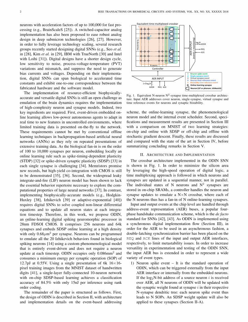
Equivalent time-multiplexed crossbar5
2
1
4
3
Controller
5 Bistability time reference event
3 Virtual synapse event
1 Neuron spike event
4 Neuron time reference event
2 Single-synapse event
REQ ACKOnline-learning synapse
Neuron (LIF or phenom. Izhikevich)
N axons
N d
end
rites
Fig. 1. Equivalent N-neuron N2-synapse time-multiplexed crossbar architec-ture. Input AER addresses cover neuron, single-synapse, virtual synapse andtime reference events for neurons and synaptic bistability.
scheme, the online-learning synapse, the phenomenologicalneuron model and the internal event scheduler. Second, speci-fications and measurement results are presented in Section IIIwith a comparison on MNIST of two learning strategies:on-chip and online with SDSP or off-chip and offline withstochastic gradient descent. Finally, these results are discussedand compared with the state of the art in Section IV, beforesummarizing concluding remarks in Section V.
II. ARCHITECTURE AND IMPLEMENTATION
The crossbar architecture implemented in the ODIN SNNis shown in Fig. 1. In order to minimize the silicon areaby leveraging the high-speed operation of digital logic, atime multiplexing approach is followed in which neurons andsynapses are updated in a sequential manner, not in parallel.The individual states of N neurons and N2 synapses arestored in on-chip SRAMs, a controller handles the neuron andsynapse updates to emulate a N×N crossbar, where each ofthe N neurons thus has a fan-in of N online-learning synapses.
Input and output events at the chip level are handled throughaddress-event representation (AER) buses, a popular four-phase handshake communication scheme, which is the de factostandard for SNNs [42], [43]. As ODIN is implemented usinga synchronous digital implementation flow (Section III), inorder for the AER to be used in an asynchronous fashion, adouble-latching synchronization barrier has been placed on theREQ and ACK lines of the input and output AER interfaces,respectively, to limit metastability issues. In order to increaseversatility in experimentation and testing of the ODIN SNN,the input AER bus is extended in order to represent a widevariety of event types.
1) Neuron spike event – It is the standard operation ofODIN, which can be triggered externally from the inputAER interface or internally from the embedded neurons.If the log2N-bit address of a source neuron i is receivedover AER, all N neurons of ODIN will be updated withthe synaptic weight found at synapse i in their respectiveN-synapse dendritic tree: each neuron spike event thusleads to N SOPs. An SDSP weight update will also beapplied to these synapses (Section II-A).
FRENKEL et al.: A 0.086-mm2 12.7-pJ/SOP 64k-SYNAPSE 256-NEURON ONLINE-LEARNING DIGITAL SPIKING NEUROMORPHIC PROCESSOR 3
1
ODINSNN
0.086mm²
320µm
27
0µ
m
Unrelated blocks
ODIN 28nm SNN
256²-synapsememory
(32kB SRAM)
256-neuron memory
(4kB SRAM)
AER
INP
UT
AER
OU
TPU
T(e
ven
ts +
mo
nit
ori
ng)
Controller and global parameters bank
SPI slave
8
REQ
ACK
ADDR
MISOMOSI
SCK
17
REQ
ACK
ADDR
CLK_EXT RST
Event scheduler(rotating FIFOs)
LIFupdate logic
Phenom. Izhikevich
update logic
SDSP
u
pd
ate
logi
c
SDSP
up
/do
wn
re
gist
ers
spk_pre
up
bistability
downDirection of change
(from SDSP registers)
Update enable (from controller)
-1 / 0 / +1generation
with overflowdetection
wCurr. synaptic weight(from syn. memory)
3 +wnext
3
3
TechnologyImplementationArea# neurons# synapses# Izhikevich behav.Online learningTime constantSupply voltageLeakage powerBaseline powerIncr. energy/SOPTot. energy/SOP
28nm FDSOIDigital
0.086mm²25664k20
SDSP, (3+1)-bit weightBiological to accelerated
0.55V – 1.0V27µW @0.55V
1.76µW/MHz @0.55V5.5pJ @0.55V9.8pJ @0.55V
Multi-
spike
(burst)
packet
decoder
Burst processing
Spike processing
Burst ISIcounter
Single-spike
packet decoder
Input 14-bitevent packets
config
32-stage FIFO
4-stage rotating FIFOs
Output events
…
clk
clk
clk
Clockgenerator
Inte
r-spike
in
terval (ISI)
Nu
mb
er o
f sp
ikes -
1Sp
iking n
eu
ron
ad
dre
ss
8 b
its3
bits
3b
its
0 0
0 0
0 0
0Sp
iking n
eu
ron
ad
dre
ss
Single-spike packet
Multi-spike (burst) packet
Synapse SRAM
Neuron SRAM
Scheduler, update logic and controller
Unrelatedblocks
b)a)
t+0t+1
t+2
t+3
t+4
t+55
t+56
Fig. 2. Block diagram of the ODIN online-learning digital spiking neuromor-phic processor, which implements the architecture shown in Fig. 1 for N=256neurons.
2) Single-synapse event – Two log2N-bit addresses areprovided in the ADDR field of the input AER interface:the address of a source neuron i and the address of adestination neuron j. This event is handled similarlyto an AER neuron spike event, but only the neuron jof ODIN will be updated, together with a single SDSPweight update to synapse i of neuron j.
3) Virtual synapse event – The log2N-bit address of a targetneuron j of ODIN and a fixed weight value are providedin the ADDR field, no synapse of ODIN is read norupdated.
4) Neuron time reference event – A specific address isused to provide an external time reference event toall neurons, which defines the time constant of theIzhikevich behaviors of the phenomenological neuronmodel (Section II-B).
5) Bistability time reference event – A specific addressis used to trigger the bistability mechanism of allsynapses (Section II-A).
Therefore, in order to represent these five event typeswith all neuron, synapse and specific time reference controladdresses, the input AER bus needs an ADDR field width of1+2log2N bits (Fig. 1).
Two operation modes can be chosen for the log2N-bit outputAER bus. The first one is the standard operation mode inwhich, as soon as one of the N neurons emits an outputspike event, the source neuron address is transmitted on thelog2N-bit ADDR field of the AER output. The second one isa non-standard operation mode for monitoring purposes of aspecific neuron or synapse, AER events containing state dataare generated. The target neuron and synapse addresses to bemonitored are configurable.
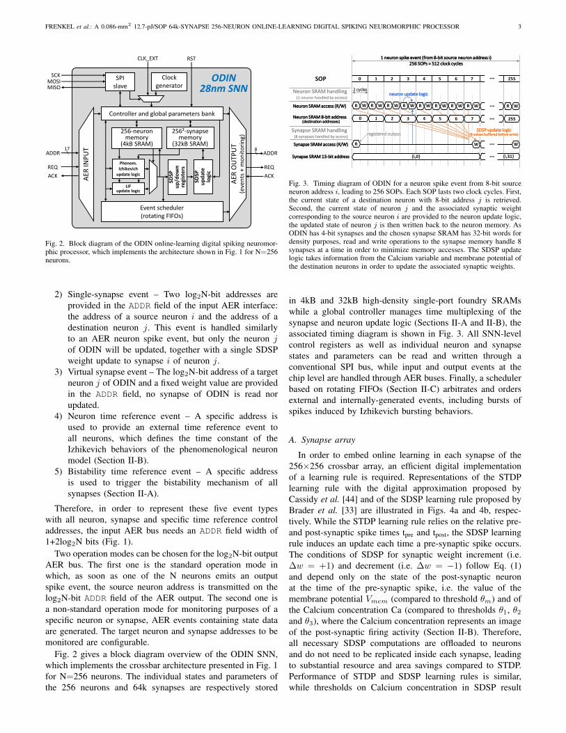
Fig. 2 gives a block diagram overview of the ODIN SNN,which implements the crossbar architecture presented in Fig. 1for N=256 neurons. The individual states and parameters ofthe 256 neurons and 64k synapses are respectively stored
1 neuron spike event (from 8-bit source neuron address i)256 SOPs = 512 clock cycles
2 cycles
R W
0SOP
Neuron SRAM access (R/W) R W R W R W R W R W R W R W
7
R
{i,0}
Synapse SRAM access (R/W)
Synapse SRAM 13-bit address
W
Neuron SRAM handling(1 neuron handled by access)
Synapse SRAM handling(8 synapses handled by access)
W
8
R W R W R W R W R W R W R W
9 10 11 12 13 14 15
{i,1}
W
Neuron SRAM 8-bit address(destination addresses)
neuron update logic
registered output
0 1 62 4
151 2 3 4 5 6 7 8 9 10 11 12 13 14…
R W
255
W
{i,31}
…
…
…
…
255
SDSP update logic(8 values buffered before write)
53
Fig. 3. Timing diagram of ODIN for a neuron spike event from 8-bit sourceneuron address i, leading to 256 SOPs. Each SOP lasts two clock cycles. First,the current state of a destination neuron with 8-bit address j is retrieved.Second, the current state of neuron j and the associated synaptic weightcorresponding to the source neuron i are provided to the neuron update logic,the updated state of neuron j is then written back to the neuron memory. AsODIN has 4-bit synapses and the chosen synapse SRAM has 32-bit words fordensity purposes, read and write operations to the synapse memory handle 8synapses at a time in order to minimize memory accesses. The SDSP updatelogic takes information from the Calcium variable and membrane potential ofthe destination neurons in order to update the associated synaptic weights.
in 4kB and 32kB high-density single-port foundry SRAMswhile a global controller manages time multiplexing of thesynapse and neuron update logic (Sections II-A and II-B), theassociated timing diagram is shown in Fig. 3. All SNN-levelcontrol registers as well as individual neuron and synapsestates and parameters can be read and written through aconventional SPI bus, while input and output events at thechip level are handled through AER buses. Finally, a schedulerbased on rotating FIFOs (Section II-C) arbitrates and ordersexternal and internally-generated events, including bursts ofspikes induced by Izhikevich bursting behaviors.
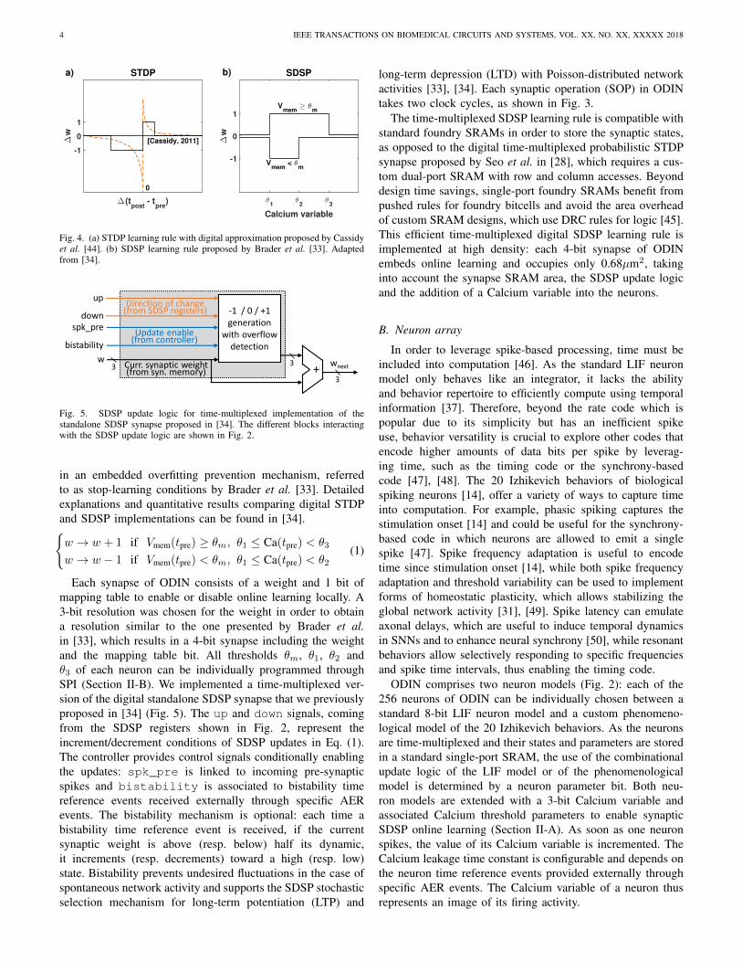
A. Synapse array
In order to embed online learning in each synapse of the256×256 crossbar array, an efficient digital implementationof a learning rule is required. Representations of the STDPlearning rule with the digital approximation proposed byCassidy et al. [44] and of the SDSP learning rule proposed byBrader et al. [33] are illustrated in Figs. 4a and 4b, respec-tively. While the STDP learning rule relies on the relative pre-and post-synaptic spike times tpre and tpost, the SDSP learningrule induces an update each time a pre-synaptic spike occurs.The conditions of SDSP for synaptic weight increment (i.e.∆w = +1) and decrement (i.e. ∆w = −1) follow Eq. (1)and depend only on the state of the post-synaptic neuronat the time of the pre-synaptic spike, i.e. the value of themembrane potential Vmem (compared to threshold θm) and ofthe Calcium concentration Ca (compared to thresholds θ1, θ2and θ3), where the Calcium concentration represents an imageof the post-synaptic firing activity (Section II-B). Therefore,all necessary SDSP computations are offloaded to neuronsand do not need to be replicated inside each synapse, leadingto substantial resource and area savings compared to STDP.Performance of STDP and SDSP learning rules is similar,while thresholds on Calcium concentration in SDSP result
4 IEEE TRANSACTIONS ON BIOMEDICAL CIRCUITS AND SYSTEMS, VOL. XX, NO. XX, XXXXX 2018
∆(tpost
- tpre
)
∆w
-1
0
1
STDP
Calcium variable
θ1
θ2
θ3
∆w
-1
0
1
SDSPa) b)
Vmem
< θm
Vmem
≥ θm
[Cassidy, 2011]
0
Fig. 4. (a) STDP learning rule with digital approximation proposed by Cassidyet al. [44]. (b) SDSP learning rule proposed by Brader et al. [33]. Adaptedfrom [34].
ODINSNN
0.093mm²
320µm
290µ
m
Unrelated blocks
ODIN 28nm SNN
256²-synapsememory
(32kB SRAM)
256-neuron memory
(4kB SRAM)
AER
INP
UT
AER
OU
TPU
T(e
ven
ts +
mo
nit
ori
ng)
Controller and parameter bank
SPI slave
8
REQ
ACK
ADDR
MISOMOSI
SCK
17
REQ
ACK
ADDR
CLK_EXT RST
Event scheduler(rotating FIFOs)
LIFupdate logic
Phenom. Izhikevich
update logic
SDSP
u
pd
ate
logi
c
SDSP
up
/do
wn
re
gist
ers
spk_pre
up
bistability
downDirection of change
(from SDSP registers)
Update enable (from controller)
-1 / 0 / +1generation
with overflowdetection
wCurr. synaptic weight(from syn. memory)
3 +wnext
3
3
TechnologyImplementationArea#Neurons#Synapses#Izhikevich behav.Online learningTime constantSupply voltageLeakage powerEnergy per syn. event
28nm FDSOIDigital
0.093mm²25664k20
SDSP, (3+1)-bit weightBiological to accelerated
0.55V – 1.0V16.5µW – 160µW
9.8pJ @0.55V
Multi-
spike
(burst)
packet
decoder
Burst processing
Spike processing
ISIcounter
Single-spike
packet decoder
Input 15-bitevent packets
config
32-stage FIFO
4-stage rotating FIFOs
Output events
…
clk
clk
clk
clock gen(max. 100MHz)
Inte
r-spike
interval (ISI)
Nu
mb
er of
spike
s -1
Spikin
g ne
uro
n
add
ress
8 bits
3 bits
4b
its
0 0
0 0
0 0
0Sp
iking n
eu
ron
ad
dre
ss
Single-spike packet
Multi-spike (burst) packet
Synapse SRAM
Neuron SRAM
Control and update logic
Unrelatedblocks
b)a)
Fig. 5. SDSP update logic for time-multiplexed implementation of thestandalone SDSP synapse proposed in [34]. The different blocks interactingwith the SDSP update logic are shown in Fig. 2.
in an embedded overfitting prevention mechanism, referredto as stop-learning conditions by Brader et al. [33]. Detailedexplanations and quantitative results comparing digital STDPand SDSP implementations can be found in [34].{w → w + 1 if Vmem(tpre) ≥ θm, θ1 ≤ Ca(tpre) < θ3
w → w − 1 if Vmem(tpre) < θm, θ1 ≤ Ca(tpre) < θ2(1)
Each synapse of ODIN consists of a weight and 1 bit ofmapping table to enable or disable online learning locally. A3-bit resolution was chosen for the weight in order to obtaina resolution similar to the one presented by Brader et al.in [33], which results in a 4-bit synapse including the weightand the mapping table bit. All thresholds θm, θ1, θ2 andθ3 of each neuron can be individually programmed throughSPI (Section II-B). We implemented a time-multiplexed ver-sion of the digital standalone SDSP synapse that we previouslyproposed in [34] (Fig. 5). The up and down signals, comingfrom the SDSP registers shown in Fig. 2, represent theincrement/decrement conditions of SDSP updates in Eq. (1).The controller provides control signals conditionally enablingthe updates: spk_pre is linked to incoming pre-synapticspikes and bistability is associated to bistability timereference events received externally through specific AERevents. The bistability mechanism is optional: each time abistability time reference event is received, if the currentsynaptic weight is above (resp. below) half its dynamic,it increments (resp. decrements) toward a high (resp. low)state. Bistability prevents undesired fluctuations in the case ofspontaneous network activity and supports the SDSP stochasticselection mechanism for long-term potentiation (LTP) and
long-term depression (LTD) with Poisson-distributed networkactivities [33], [34]. Each synaptic operation (SOP) in ODINtakes two clock cycles, as shown in Fig. 3.
The time-multiplexed SDSP learning rule is compatible withstandard foundry SRAMs in order to store the synaptic states,as opposed to the digital time-multiplexed probabilistic STDPsynapse proposed by Seo et al. in [28], which requires a cus-tom dual-port SRAM with row and column accesses. Beyonddesign time savings, single-port foundry SRAMs benefit frompushed rules for foundry bitcells and avoid the area overheadof custom SRAM designs, which use DRC rules for logic [45].This efficient time-multiplexed digital SDSP learning rule isimplemented at high density: each 4-bit synapse of ODINembeds online learning and occupies only 0.68µm2, takinginto account the synapse SRAM area, the SDSP update logicand the addition of a Calcium variable into the neurons.
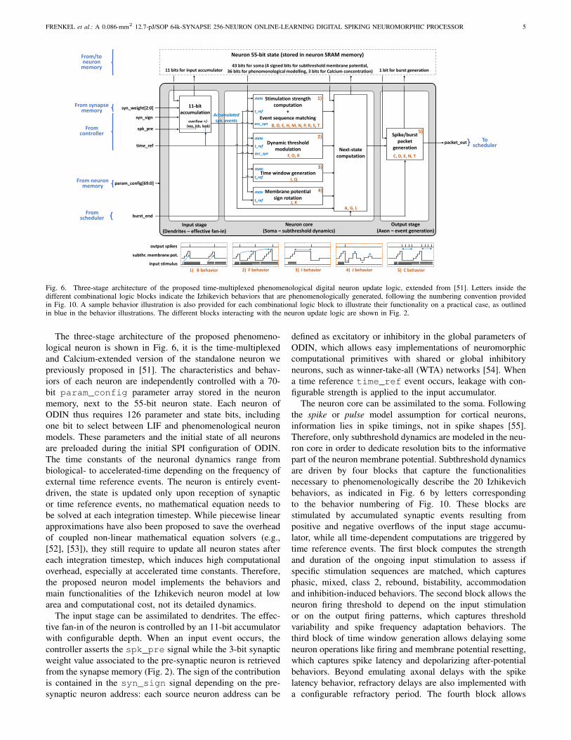
B. Neuron array
In order to leverage spike-based processing, time must beincluded into computation [46]. As the standard LIF neuronmodel only behaves like an integrator, it lacks the abilityand behavior repertoire to efficiently compute using temporalinformation [37]. Therefore, beyond the rate code which ispopular due to its simplicity but has an inefficient spikeuse, behavior versatility is crucial to explore other codes thatencode higher amounts of data bits per spike by leverag-ing time, such as the timing code or the synchrony-basedcode [47], [48]. The 20 Izhikevich behaviors of biologicalspiking neurons [14], offer a variety of ways to capture timeinto computation. For example, phasic spiking captures thestimulation onset [14] and could be useful for the synchrony-based code in which neurons are allowed to emit a singlespike [47]. Spike frequency adaptation is useful to encodetime since stimulation onset [14], while both spike frequencyadaptation and threshold variability can be used to implementforms of homeostatic plasticity, which allows stabilizing theglobal network activity [31], [49]. Spike latency can emulateaxonal delays, which are useful to induce temporal dynamicsin SNNs and to enhance neural synchrony [50], while resonantbehaviors allow selectively responding to specific frequenciesand spike time intervals, thus enabling the timing code.
ODIN comprises two neuron models (Fig. 2): each of the256 neurons of ODIN can be individually chosen between astandard 8-bit LIF neuron model and a custom phenomeno-logical model of the 20 Izhikevich behaviors. As the neuronsare time-multiplexed and their states and parameters are storedin a standard single-port SRAM, the use of the combinationalupdate logic of the LIF model or of the phenomenologicalmodel is determined by a neuron parameter bit. Both neu-ron models are extended with a 3-bit Calcium variable andassociated Calcium threshold parameters to enable synapticSDSP online learning (Section II-A). As soon as one neuronspikes, the value of its Calcium variable is incremented. TheCalcium leakage time constant is configurable and depends onthe neuron time reference events provided externally throughspecific AER events. The Calcium variable of a neuron thusrepresents an image of its firing activity.
FRENKEL et al.: A 0.086-mm2 12.7-pJ/SOP 64k-SYNAPSE 256-NEURON ONLINE-LEARNING DIGITAL SPIKING NEUROMORPHIC PROCESSOR 5
overflow +/-(exc, inh, leak)
Input stage(Dendrites – effective fan-in)
Neuron core(Soma – subthreshold dynamics)
Spike/burstpacket
generationpacket_out
Output stage(Axon – event generation)
Neuron 55-bit state (stored in neuron SRAM memory)
1 bit for burst generation43 bits for soma (4 signed bits for subthreshold membrane potential,
36 bits for phenomenological modelling, 3 bits for Calcium concentration)
Stimulation strength computation
+Event sequence matching
Dynamic threshold modulation
Time window generation
Membrane potentialsign rotationt_ref
t_ref
t_ref
t_ref
acc_syn
state
state
state
state
Next-statecomputation
11-bitaccumulation
C, D, E, N, T
A, G, L
B, D, E, H, M, N, P, R, S, T
F, O, R
I, Q
J, K
acc_syn
syn_sign
time_ref
spk_pre
syn_weight[2:0]
param_config[69:0]
11 bits for input accumulator
burst_end
From controller
From synapse memory
From neuron memory
From/to neuron
memory
From scheduler
To scheduler
Accumulatedsyn. events
1) B behavior 2) F behavior 3) I behavior 4) J behavior 5) C behavior
1)
2)
3)
4)
5)
+
-+
-
output spikes
input stimulus
subthr. membrane pot.
Fig. 6. Three-stage architecture of the proposed time-multiplexed phenomenological digital neuron update logic, extended from [51]. Letters inside thedifferent combinational logic blocks indicate the Izhikevich behaviors that are phenomenologically generated, following the numbering convention providedin Fig. 10. A sample behavior illustration is also provided for each combinational logic block to illustrate their functionality on a practical case, as outlinedin blue in the behavior illustrations. The different blocks interacting with the neuron update logic are shown in Fig. 2.
The three-stage architecture of the proposed phenomeno-logical neuron is shown in Fig. 6, it is the time-multiplexedand Calcium-extended version of the standalone neuron wepreviously proposed in [51]. The characteristics and behav-iors of each neuron are independently controlled with a 70-bit param_config parameter array stored in the neuronmemory, next to the 55-bit neuron state. Each neuron ofODIN thus requires 126 parameter and state bits, includingone bit to select between LIF and phenomenological neuronmodels. These parameters and the initial state of all neuronsare preloaded during the initial SPI configuration of ODIN.The time constants of the neuronal dynamics range frombiological- to accelerated-time depending on the frequency ofexternal time reference events. The neuron is entirely event-driven, the state is updated only upon reception of synapticor time reference events, no mathematical equation needs tobe solved at each integration timestep. While piecewise linearapproximations have also been proposed to save the overheadof coupled non-linear mathematical equation solvers (e.g.,[52], [53]), they still require to update all neuron states aftereach integration timestep, which induces high computationaloverhead, especially at accelerated time constants. Therefore,the proposed neuron model implements the behaviors andmain functionalities of the Izhikevich neuron model at lowarea and computational cost, not its detailed dynamics.
The input stage can be assimilated to dendrites. The effec-tive fan-in of the neuron is controlled by an 11-bit accumulatorwith configurable depth. When an input event occurs, thecontroller asserts the spk_pre signal while the 3-bit synapticweight value associated to the pre-synaptic neuron is retrievedfrom the synapse memory (Fig. 2). The sign of the contributionis contained in the syn_sign signal depending on the pre-synaptic neuron address: each source neuron address can be
defined as excitatory or inhibitory in the global parameters ofODIN, which allows easy implementations of neuromorphiccomputational primitives with shared or global inhibitoryneurons, such as winner-take-all (WTA) networks [54]. Whena time reference time_ref event occurs, leakage with con-figurable strength is applied to the input accumulator.
The neuron core can be assimilated to the soma. Followingthe spike or pulse model assumption for cortical neurons,information lies in spike timings, not in spike shapes [55].Therefore, only subthreshold dynamics are modeled in the neu-ron core in order to dedicate resolution bits to the informativepart of the neuron membrane potential. Subthreshold dynamicsare driven by four blocks that capture the functionalitiesnecessary to phenomenologically describe the 20 Izhikevichbehaviors, as indicated in Fig. 6 by letters correspondingto the behavior numbering of Fig. 10. These blocks arestimulated by accumulated synaptic events resulting frompositive and negative overflows of the input stage accumu-lator, while all time-dependent computations are triggered bytime reference events. The first block computes the strengthand duration of the ongoing input stimulation to assess ifspecific stimulation sequences are matched, which capturesphasic, mixed, class 2, rebound, bistability, accommodationand inhibition-induced behaviors. The second block allows theneuron firing threshold to depend on the input stimulationor on the output firing patterns, which captures thresholdvariability and spike frequency adaptation behaviors. Thethird block of time window generation allows delaying someneuron operations like firing and membrane potential resetting,which captures spike latency and depolarizing after-potentialbehaviors. Beyond emulating axonal delays with the spikelatency behavior, refractory delays are also implemented witha configurable refractory period. The fourth block allows
6 IEEE TRANSACTIONS ON BIOMEDICAL CIRCUITS AND SYSTEMS, VOL. XX, NO. XX, XXXXX 2018
1
ODINSNN
0.086mm²
320µm
27
0µ
m
Unrelated blocks
ODIN 28nm SNN
256²-synapsememory
(32kB SRAM)
256-neuron memory
(4kB SRAM)
AER
INP
UT
AER
OU
TPU
T(e
ven
ts +
mo
nit
ori
ng)
Controller and global parameters bank
SPI slave
8
REQ
ACK
ADDR
MISOMOSI
SCK
17
REQ
ACK
ADDR
CLK_EXT RST
Event scheduler(rotating FIFOs)
LIFupdate logic
Phenom. Izhikevich
update logic
SDSP
u
pd
ate
logi
c
SDSP
up
/do
wn
re
gist
ers
spk_pre
up
bistability
downDirection of change
(from SDSP registers)
Update enable (from controller)
-1 / 0 / +1generation
with overflowdetection
wCurr. synaptic weight(from syn. memory)
3 +wnext
3
3
TechnologyImplementationArea# neurons# synapses# Izhikevich behav.Online learningTime constantSupply voltageLeakage powerEnergy per SOP
28nm FDSOIDigital
0.086mm²25664k20
SDSP, (3+1)-bit weightBiological to accelerated
0.55V – 1.0V16.5µW – 160µW
9.8pJ @0.55V
Multi-
spike
(burst)
packet
decoder
Burst processing
Spike processing
Burst ISIcounter
Single-spike
packet decoder
Input 14-bitevent packets
config
32-stage FIFO
4-stage rotating FIFOs
Output events
…
clk
clk
clk
clock gen(max. 100MHz)
Inte
r-spike
in
terval (ISI)
Nu
mb
er o
f sp
ikes -
1Sp
iking n
eu
ron
ad
dre
ss
8 b
its3
bits
3b
its
0 0
0 0
0 0
0Sp
iking n
eu
ron
ad
dre
ss
Single-spike packet
Multi-spike (burst) packet
Synapse SRAM
Neuron SRAM
Scheduler, update logic and controller
Unrelatedblocks
b)a)
t+0t+1
t+2
t+3
t+4
t+55
t+56
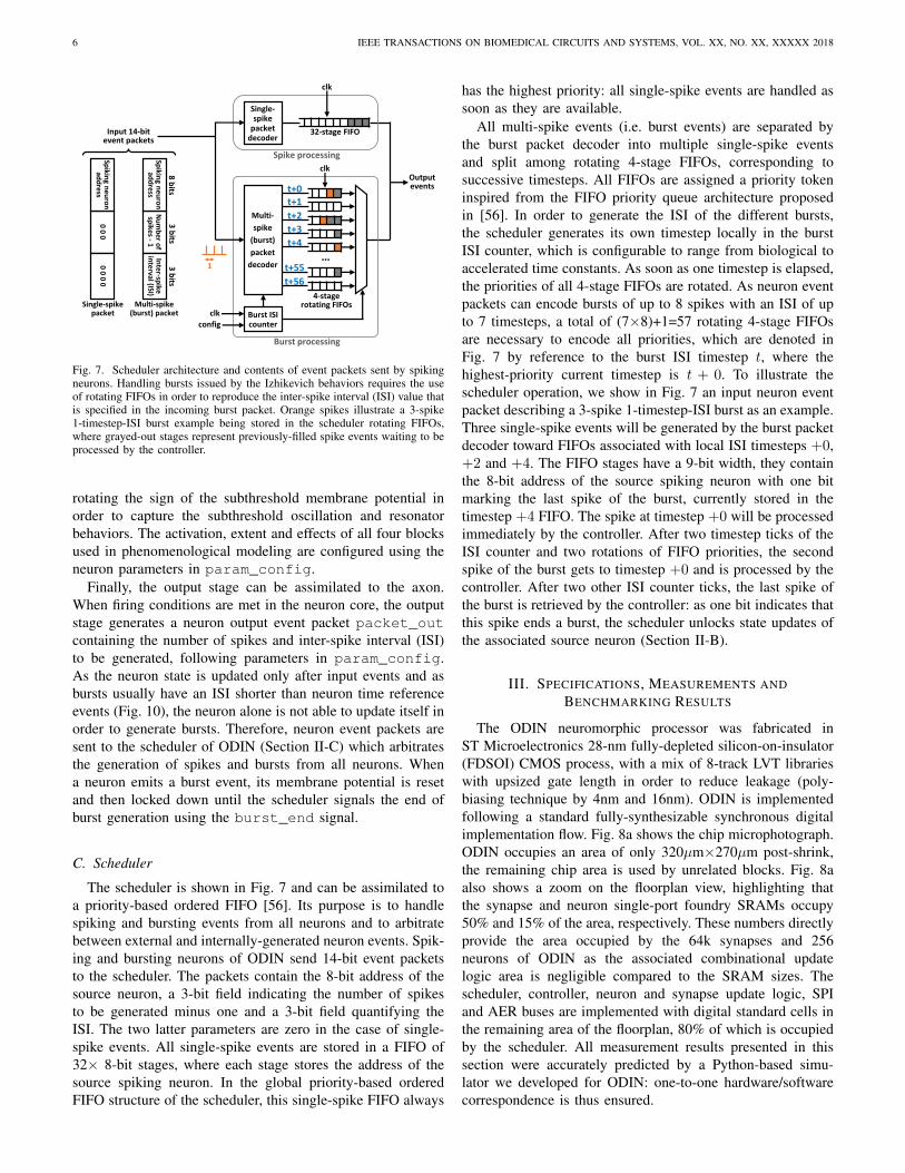
Fig. 7. Scheduler architecture and contents of event packets sent by spikingneurons. Handling bursts issued by the Izhikevich behaviors requires the useof rotating FIFOs in order to reproduce the inter-spike interval (ISI) value thatis specified in the incoming burst packet. Orange spikes illustrate a 3-spike1-timestep-ISI burst example being stored in the scheduler rotating FIFOs,where grayed-out stages represent previously-filled spike events waiting to beprocessed by the controller.
rotating the sign of the subthreshold membrane potential inorder to capture the subthreshold oscillation and resonatorbehaviors. The activation, extent and effects of all four blocksused in phenomenological modeling are configured using theneuron parameters in param_config.
Finally, the output stage can be assimilated to the axon.When firing conditions are met in the neuron core, the outputstage generates a neuron output event packet packet_outcontaining the number of spikes and inter-spike interval (ISI)to be generated, following parameters in param_config.As the neuron state is updated only after input events and asbursts usually have an ISI shorter than neuron time referenceevents (Fig. 10), the neuron alone is not able to update itself inorder to generate bursts. Therefore, neuron event packets aresent to the scheduler of ODIN (Section II-C) which arbitratesthe generation of spikes and bursts from all neurons. Whena neuron emits a burst event, its membrane potential is resetand then locked down until the scheduler signals the end ofburst generation using the burst_end signal.
C. Scheduler
The scheduler is shown in Fig. 7 and can be assimilated toa priority-based ordered FIFO [56]. Its purpose is to handlespiking and bursting events from all neurons and to arbitratebetween external and internally-generated neuron events. Spik-ing and bursting neurons of ODIN send 14-bit event packetsto the scheduler. The packets contain the 8-bit address of thesource neuron, a 3-bit field indicating the number of spikesto be generated minus one and a 3-bit field quantifying theISI. The two latter parameters are zero in the case of single-spike events. All single-spike events are stored in a FIFO of32× 8-bit stages, where each stage stores the address of thesource spiking neuron. In the global priority-based orderedFIFO structure of the scheduler, this single-spike FIFO always
has the highest priority: all single-spike events are handled assoon as they are available.
All multi-spike events (i.e. burst events) are separated bythe burst packet decoder into multiple single-spike eventsand split among rotating 4-stage FIFOs, corresponding tosuccessive timesteps. All FIFOs are assigned a priority tokeninspired from the FIFO priority queue architecture proposedin [56]. In order to generate the ISI of the different bursts,the scheduler generates its own timestep locally in the burstISI counter, which is configurable to range from biological toaccelerated time constants. As soon as one timestep is elapsed,the priorities of all 4-stage FIFOs are rotated. As neuron eventpackets can encode bursts of up to 8 spikes with an ISI of upto 7 timesteps, a total of (7×8)+1=57 rotating 4-stage FIFOsare necessary to encode all priorities, which are denoted inFig. 7 by reference to the burst ISI timestep t, where thehighest-priority current timestep is t + 0. To illustrate thescheduler operation, we show in Fig. 7 an input neuron eventpacket describing a 3-spike 1-timestep-ISI burst as an example.Three single-spike events will be generated by the burst packetdecoder toward FIFOs associated with local ISI timesteps +0,+2 and +4. The FIFO stages have a 9-bit width, they containthe 8-bit address of the source spiking neuron with one bitmarking the last spike of the burst, currently stored in thetimestep +4 FIFO. The spike at timestep +0 will be processedimmediately by the controller. After two timestep ticks of theISI counter and two rotations of FIFO priorities, the secondspike of the burst gets to timestep +0 and is processed by thecontroller. After two other ISI counter ticks, the last spike ofthe burst is retrieved by the controller: as one bit indicates thatthis spike ends a burst, the scheduler unlocks state updates ofthe associated source neuron (Section II-B).
III. SPECIFICATIONS, MEASUREMENTS ANDBENCHMARKING RESULTS
The ODIN neuromorphic processor was fabricated inST Microelectronics 28-nm fully-depleted silicon-on-insulator(FDSOI) CMOS process, with a mix of 8-track LVT librarieswith upsized gate length in order to reduce leakage (poly-biasing technique by 4nm and 16nm). ODIN is implementedfollowing a standard fully-synthesizable synchronous digitalimplementation flow. Fig. 8a shows the chip microphotograph.ODIN occupies an area of only 320µm×270µm post-shrink,the remaining chip area is used by unrelated blocks. Fig. 8aalso shows a zoom on the floorplan view, highlighting thatthe synapse and neuron single-port foundry SRAMs occupy50% and 15% of the area, respectively. These numbers directlyprovide the area occupied by the 64k synapses and 256neurons of ODIN as the associated combinational updatelogic area is negligible compared to the SRAM sizes. Thescheduler, controller, neuron and synapse update logic, SPIand AER buses are implemented with digital standard cells inthe remaining area of the floorplan, 80% of which is occupiedby the scheduler. All measurement results presented in thissection were accurately predicted by a Python-based simu-lator we developed for ODIN: one-to-one hardware/softwarecorrespondence is thus ensured.
FRENKEL et al.: A 0.086-mm2 12.7-pJ/SOP 64k-SYNAPSE 256-NEURON ONLINE-LEARNING DIGITAL SPIKING NEUROMORPHIC PROCESSOR 7
1
ODIN 28nm SNN
256²-synapsememory
(32kB SRAM)
256-neuron memory
(4kB SRAM)
AER
INP
UT
AER
OU
TPU
T(e
ven
ts +
mo
nit
ori
ng)
Controller and global parameters bank
SPI slave
8
REQ
ACK
ADDR
MISOMOSI
SCK
17
REQ
ACK
ADDR
CLK_EXT RST
Event scheduler(rotating FIFOs)
LIFupdate logic
Phenom. Izhikevich
update logic
SDSP
u
pd
ate
logi
c
SDSP
up
/do
wn
re
gist
ers
spk_pre
up
bistability
downDirection of change
(from SDSP registers)
Update enable (from controller)
-1 / 0 / +1generation
with overflowdetection
wCurr. synaptic weight(from syn. memory)
3 +wnext
3
3
TechnologyImplementationArea# neurons# synapses# Izhikevich behav.Online learningTime constantSupply voltageLeakage power (Pleak)Idle power (Pidle)Incr. energy/SOP (ESOP)Global energy/SOP (Etot,SOP)
28nm FDSOIDigital
0.086mm²25664k20
SDSP, (3+1)-bit weightBiological to accelerated
0.55V – 1.0V27.3µW @0.55V
1.78µW/MHz @0.55V8.43pJ @0.55V
>12.7pJ @0.55V
Multi-
spike
(burst)
packet
decoder
Burst processing
Spike processing
Burst ISIcounter
Single-spike
packet decoder
Input 14-bitevent packets
config
32-stage FIFO
4-stage rotating FIFOs
Output events
…
clk
clk
clk
Clockgenerator
Inte
r-spike
interval (ISI)
Nu
mb
er o
f sp
ikes -1
Spikin
g ne
uro
n
add
ress
8 bits
3 b
its3
bits
0 0 0
00
0 0Sp
iking n
eu
ron
ad
dre
ss
Single-spike packet
Multi-spike (burst) packet
ODINSNN
0.086mm²
320µm
270µ
m
Unrelated blocks
SynapseSRAM
Neuron SRAM
Scheduler, update logic and controller
Unrelatedblocks
b)a)
t+0t+1
t+2
t+3
t+4
t+55
t+56
Fig. 8. (a) Chip microphotograph with zoom on floorplan view. Chip areaoutside the 320µm×270µm of the ODIN neuromorphic processor is occupiedby unrelated blocks. (b) Specifications and measurements. Pleak, Pidle andESOP are parameters of the ODIN power consumption model in Eq. (2).
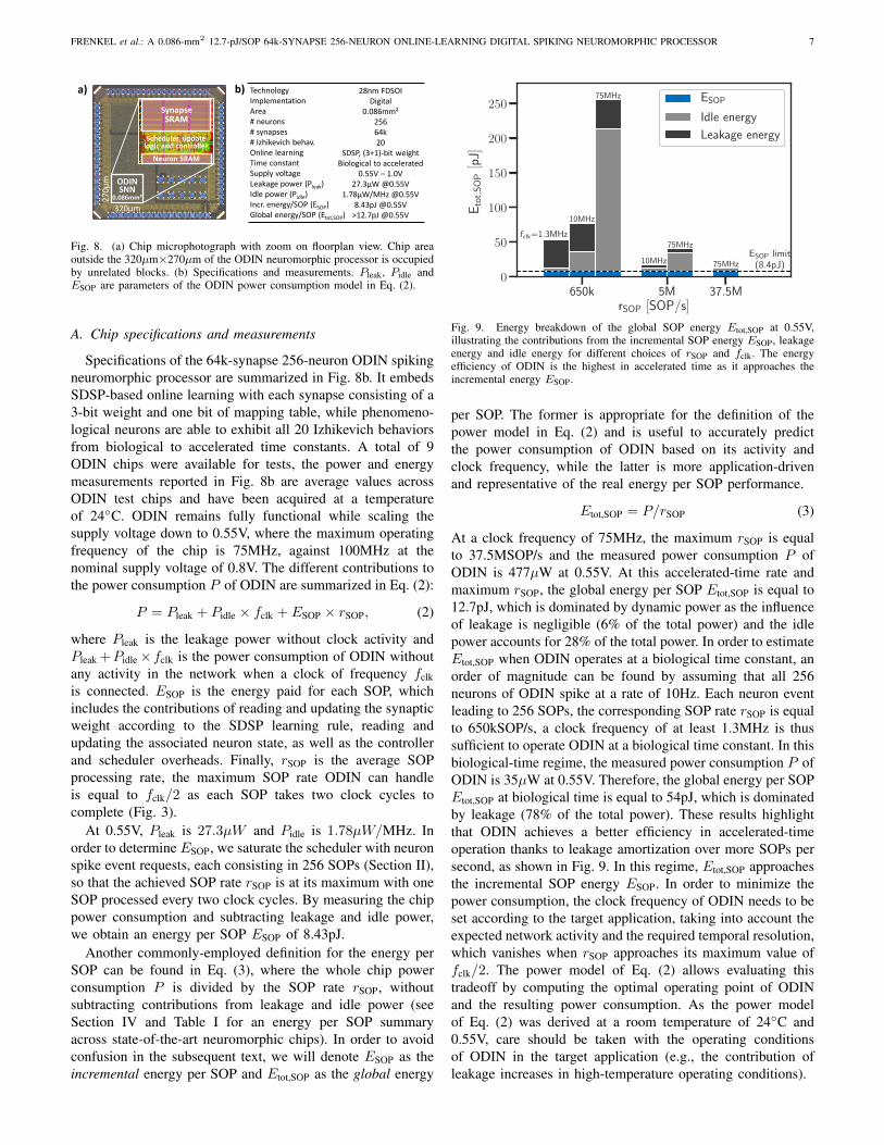
A. Chip specifications and measurements
Specifications of the 64k-synapse 256-neuron ODIN spikingneuromorphic processor are summarized in Fig. 8b. It embedsSDSP-based online learning with each synapse consisting of a3-bit weight and one bit of mapping table, while phenomeno-logical neurons are able to exhibit all 20 Izhikevich behaviorsfrom biological to accelerated time constants. A total of 9ODIN chips were available for tests, the power and energymeasurements reported in Fig. 8b are average values acrossODIN test chips and have been acquired at a temperatureof 24◦C. ODIN remains fully functional while scaling thesupply voltage down to 0.55V, where the maximum operatingfrequency of the chip is 75MHz, against 100MHz at thenominal supply voltage of 0.8V. The different contributions tothe power consumption P of ODIN are summarized in Eq. (2):
P = Pleak + Pidle × fclk + ESOP × rSOP, (2)
where Pleak is the leakage power without clock activity andPleak +Pidle×fclk is the power consumption of ODIN withoutany activity in the network when a clock of frequency fclkis connected. ESOP is the energy paid for each SOP, whichincludes the contributions of reading and updating the synapticweight according to the SDSP learning rule, reading andupdating the associated neuron state, as well as the controllerand scheduler overheads. Finally, rSOP is the average SOPprocessing rate, the maximum SOP rate ODIN can handleis equal to fclk/2 as each SOP takes two clock cycles tocomplete (Fig. 3).
At 0.55V, Pleak is 27.3µW and Pidle is 1.78µW/MHz. Inorder to determine ESOP, we saturate the scheduler with neuronspike event requests, each consisting in 256 SOPs (Section II),so that the achieved SOP rate rSOP is at its maximum with oneSOP processed every two clock cycles. By measuring the chippower consumption and subtracting leakage and idle power,we obtain an energy per SOP ESOP of 8.43pJ.
Another commonly-employed definition for the energy perSOP can be found in Eq. (3), where the whole chip powerconsumption P is divided by the SOP rate rSOP, withoutsubtracting contributions from leakage and idle power (seeSection IV and Table I for an energy per SOP summaryacross state-of-the-art neuromorphic chips). In order to avoidconfusion in the subsequent text, we will denote ESOP as theincremental energy per SOP and Etot,SOP as the global energy
650k 5M 37.5MrSOP [SOP/s]
0
50
100
150
200
250
Etot,SOP[pJ]
fclk=1.3MHz
10MHz
75MHz
10MHz
75MHz
75MHzESOP limit(8.4pJ)
ESOP
Idle energy
Leakage energy
Fig. 9. Energy breakdown of the global SOP energy Etot,SOP at 0.55V,illustrating the contributions from the incremental SOP energy ESOP, leakageenergy and idle energy for different choices of rSOP and fclk. The energyefficiency of ODIN is the highest in accelerated time as it approaches theincremental energy ESOP.
per SOP. The former is appropriate for the definition of thepower model in Eq. (2) and is useful to accurately predictthe power consumption of ODIN based on its activity andclock frequency, while the latter is more application-drivenand representative of the real energy per SOP performance.
Etot,SOP = P/rSOP (3)
At a clock frequency of 75MHz, the maximum rSOP is equalto 37.5MSOP/s and the measured power consumption P ofODIN is 477µW at 0.55V. At this accelerated-time rate andmaximum rSOP, the global energy per SOP Etot,SOP is equal to12.7pJ, which is dominated by dynamic power as the influenceof leakage is negligible (6% of the total power) and the idlepower accounts for 28% of the total power. In order to estimateEtot,SOP when ODIN operates at a biological time constant, anorder of magnitude can be found by assuming that all 256neurons of ODIN spike at a rate of 10Hz. Each neuron eventleading to 256 SOPs, the corresponding SOP rate rSOP is equalto 650kSOP/s, a clock frequency of at least 1.3MHz is thussufficient to operate ODIN at a biological time constant. In thisbiological-time regime, the measured power consumption P ofODIN is 35µW at 0.55V. Therefore, the global energy per SOPEtot,SOP at biological time is equal to 54pJ, which is dominatedby leakage (78% of the total power). These results highlightthat ODIN achieves a better efficiency in accelerated-timeoperation thanks to leakage amortization over more SOPs persecond, as shown in Fig. 9. In this regime, Etot,SOP approachesthe incremental SOP energy ESOP. In order to minimize thepower consumption, the clock frequency of ODIN needs to beset according to the target application, taking into account theexpected network activity and the required temporal resolution,which vanishes when rSOP approaches its maximum value offclk/2. The power model of Eq. (2) allows evaluating thistradeoff by computing the optimal operating point of ODINand the resulting power consumption. As the power modelof Eq. (2) was derived at a room temperature of 24◦C and0.55V, care should be taken with the operating conditionsof ODIN in the target application (e.g., the contribution ofleakage increases in high-temperature operating conditions).
8 IEEE TRANSACTIONS ON BIOMEDICAL CIRCUITS AND SYSTEMS, VOL. XX, NO. XX, XXXXX 2018
20ms
output spikes
subthr. membrane pot.
input spikes and time ref.
(A) Tonic spiking
20ms
(B) Phasic spiking
20ms
(C) Tonic bursting
20ms
(D) Phasic bursting
20ms
(E) Mixed mode
20ms
(F) Spike freq. adapt
20ms
(G) Class 1 excitable
20ms
(H) Class 2 excitable
20ms
(I) Spike latency
20ms
(J) Subthreshold oscillations
20ms
(K) Resonator
20ms
(L) Integrator
20ms
(M) Rebound spike
20ms
(N) Rebound burst
20ms
(O) Threshold variability
20ms
(P) Bistability
20ms
(Q) Depolarizing after-potential
20ms
(R) Accommodation
20ms
(S) Inhibition-induced spiking
20ms
(T) Inhibition-induced bursting
Fig. 10. Silicon validation of the 20 Izhikevich behaviors with biological time constant in ODIN. Scale references of 20ms are provided next to each of the20 behaviors and closely match those of the original Izhikevich behaviors figure in [14].
Pre-synaptic spikes and bistability time reference events
0
4
7Synaptic weight ( )
0m
Post-synaptic neuron subthreshold membrane potential ( ) and output spike events
Time [ms]0 50 100 150 200 250 300 350 400 450
0123
Calcium variable ( )
Firing threshold
Bistability threshold
Learning realization without LTP transitionPre-synaptic spikes and bistability time reference events
0
4
7Synaptic weight ( )
0m
Post-synaptic neuron subthreshold membrane potential ( ) and output spike events
Time [ms]0 50 100 150 200 250 300 350 400 450
0123
Calcium variable ( )
Learning realization with LTP transition
Fig. 11. Silicon validation of stochastic synaptic selection mechanism of the SDSP learning rule. Left: no realization of a long-term potentiation (LTP). Right:realization of an LTP after 200ms. All stimuli have been applied to a neuron in LIF configuration and generated with identical Poisson-distributed statistics:the pre-synaptic neuron fires at a rate of 70Hz, while the post-synaptic neuron fires at a rate of 40Hz. Bistability time reference events are shown in dottedorange lines at a frequency of 20Hz next to the pre-synaptic spikes. The bistability threshold at half the synaptic weight dynamic represents the value above(resp. below) which the synaptic weight increments (resp. decrements) to a high (resp. low) state upon bistability events. The SDSP conditions for weightincrement and decrement from the post-synaptic neuron (up and down signals in Fig. 5) are shown next to the Calcium variable with red and blue areas,respectively. Non-colored areas of the Calcium variable are associated with stop-learning conditions.
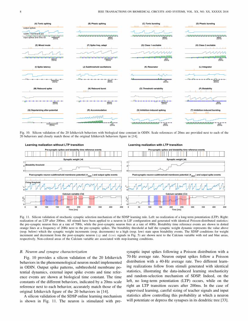
B. Neuron and synapse characterizationFig. 10 provides a silicon validation of the 20 Izhikevich
behaviors in the phenomenological neuron model implementedin ODIN. Output spike patterns, subthreshold membrane po-tential dynamics, external input spike events and time refer-ence events are shown at biological time constant. The timeconstants of the different behaviors, indicated by a 20ms scalereference next to each behavior, accurately match those of theoriginal Izhikevich figure of the 20 behaviors in [14].
A silicon validation of the SDSP online learning mechanismis shown in Fig. 11. The neuron is stimulated with pre-
synaptic input spikes following a Poisson distribution with a70-Hz average rate. Neuron output spikes follow a Poissondistribution with a 40-Hz average rate. Two different learn-ing realizations follow from stimuli generated with identicalstatistics, illustrating the data-induced learning stochasticityand random-selection mechanism of SDSP. Indeed, on theleft, no long-term potentiation (LTP) occurs, while on theright an LTP transition occurs after 200ms. In the case ofsupervised learning, careful sizing of teacher signals and inputstatistics allow controlling this probability at which a neuronwill potentiate or depress the synapses in its dendritic tree [33].
FRENKEL et al.: A 0.086-mm2 12.7-pJ/SOP 64k-SYNAPSE 256-NEURON ONLINE-LEARNING DIGITAL SPIKING NEUROMORPHIC PROCESSOR 9
Compression from 28x28 to 16x16 pixels
Deskewing Soft thresholding
10-neuron SNN (ODIN)
……
16x16=256input synapses
with 3-bit weight per neuron
MNIST pre-processing steps
Conversion of pixels to rate-based Poisson-
distributed spike trains during the SDSP learning
phase or other coding schemes during inference
Teacher signal(for training only)
…
On-chip online learning setupOff-chip offline learning setup
…
……
16x16=256input 3-bit
weights per neuron
Labels
…
…
10-neuron ANN (Keras/TensorFlow)
b)a)
10-neuron SNN (ODIN)
……
…
…
Training Inference
Weight upload
Training + inference
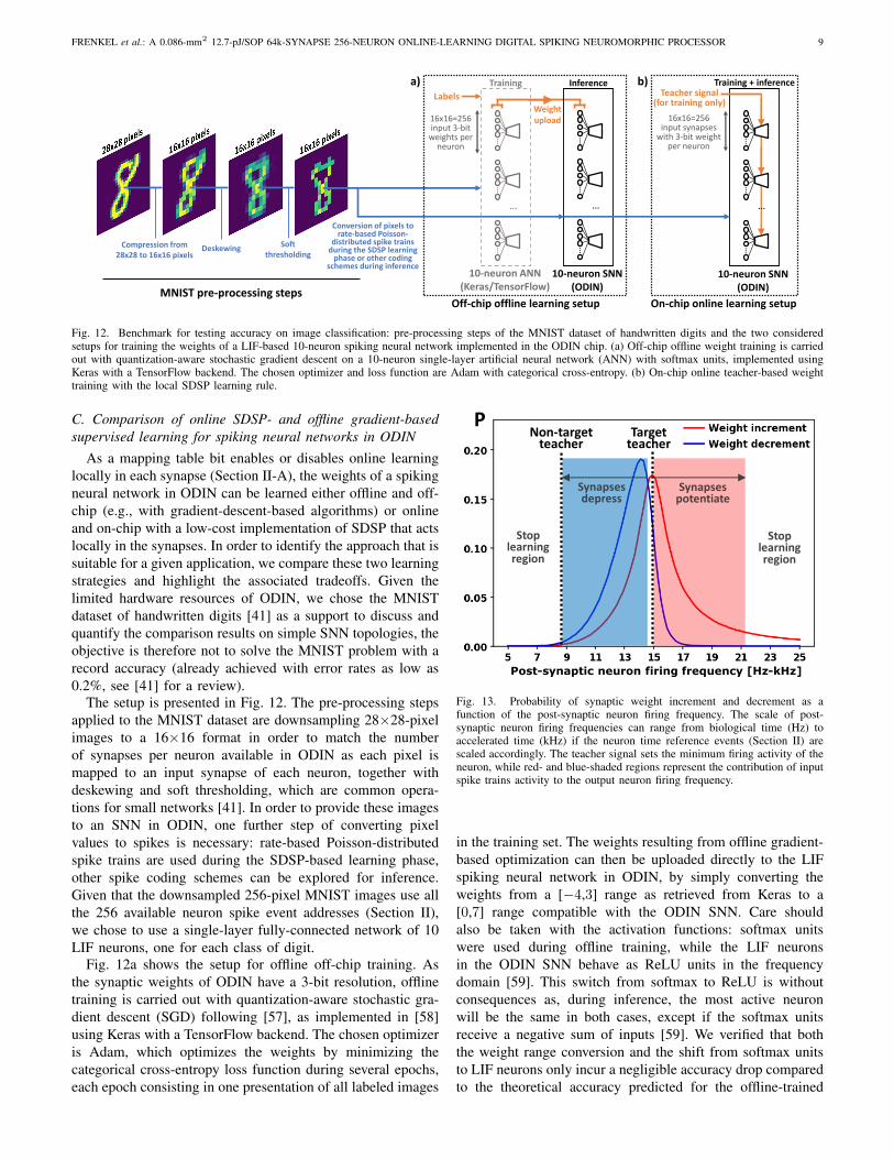
Fig. 12. Benchmark for testing accuracy on image classification: pre-processing steps of the MNIST dataset of handwritten digits and the two consideredsetups for training the weights of a LIF-based 10-neuron spiking neural network implemented in the ODIN chip. (a) Off-chip offline weight training is carriedout with quantization-aware stochastic gradient descent on a 10-neuron single-layer artificial neural network (ANN) with softmax units, implemented usingKeras with a TensorFlow backend. The chosen optimizer and loss function are Adam with categorical cross-entropy. (b) On-chip online teacher-based weighttraining with the local SDSP learning rule.
C. Comparison of online SDSP- and offline gradient-basedsupervised learning for spiking neural networks in ODIN
As a mapping table bit enables or disables online learninglocally in each synapse (Section II-A), the weights of a spikingneural network in ODIN can be learned either offline and off-chip (e.g., with gradient-descent-based algorithms) or onlineand on-chip with a low-cost implementation of SDSP that actslocally in the synapses. In order to identify the approach that issuitable for a given application, we compare these two learningstrategies and highlight the associated tradeoffs. Given thelimited hardware resources of ODIN, we chose the MNISTdataset of handwritten digits [41] as a support to discuss andquantify the comparison results on simple SNN topologies, theobjective is therefore not to solve the MNIST problem with arecord accuracy (already achieved with error rates as low as0.2%, see [41] for a review).
The setup is presented in Fig. 12. The pre-processing stepsapplied to the MNIST dataset are downsampling 28×28-pixelimages to a 16×16 format in order to match the numberof synapses per neuron available in ODIN as each pixel ismapped to an input synapse of each neuron, together withdeskewing and soft thresholding, which are common opera-tions for small networks [41]. In order to provide these imagesto an SNN in ODIN, one further step of converting pixelvalues to spikes is necessary: rate-based Poisson-distributedspike trains are used during the SDSP-based learning phase,other spike coding schemes can be explored for inference.Given that the downsampled 256-pixel MNIST images use allthe 256 available neuron spike event addresses (Section II),we chose to use a single-layer fully-connected network of 10LIF neurons, one for each class of digit.
Fig. 12a shows the setup for offline off-chip training. Asthe synaptic weights of ODIN have a 3-bit resolution, offlinetraining is carried out with quantization-aware stochastic gra-dient descent (SGD) following [57], as implemented in [58]using Keras with a TensorFlow backend. The chosen optimizeris Adam, which optimizes the weights by minimizing thecategorical cross-entropy loss function during several epochs,each epoch consisting in one presentation of all labeled images
Non-target teacher
Target teacher
Stop learning region
Stop learning region
Synapses potentiate
Synapses depress
Post-synaptic neuron firing frequency [Hz-kHz]
P
Fig. 13. Probability of synaptic weight increment and decrement as afunction of the post-synaptic neuron firing frequency. The scale of post-synaptic neuron firing frequencies can range from biological time (Hz) toaccelerated time (kHz) if the neuron time reference events (Section II) arescaled accordingly. The teacher signal sets the minimum firing activity of theneuron, while red- and blue-shaded regions represent the contribution of inputspike trains activity to the output neuron firing frequency.
in the training set. The weights resulting from offline gradient-based optimization can then be uploaded directly to the LIFspiking neural network in ODIN, by simply converting theweights from a [−4,3] range as retrieved from Keras to a[0,7] range compatible with the ODIN SNN. Care shouldalso be taken with the activation functions: softmax unitswere used during offline training, while the LIF neuronsin the ODIN SNN behave as ReLU units in the frequencydomain [59]. This switch from softmax to ReLU is withoutconsequences as, during inference, the most active neuronwill be the same in both cases, except if the softmax unitsreceive a negative sum of inputs [59]. We verified that boththe weight range conversion and the shift from softmax unitsto LIF neurons only incur a negligible accuracy drop comparedto the theoretical accuracy predicted for the offline-trained
10 IEEE TRANSACTIONS ON BIOMEDICAL CIRCUITS AND SYSTEMS, VOL. XX, NO. XX, XXXXX 2018
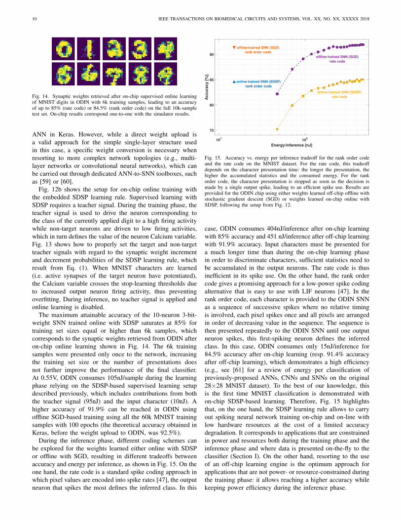
Fig. 14. Synaptic weights retrieved after on-chip supervised online learningof MNIST digits in ODIN with 6k training samples, leading to an accuracyof up to 85% (rate code) or 84.5% (rank order code) on the full 10k-sampletest set. On-chip results correspond one-to-one with the simulator results.
ANN in Keras. However, while a direct weight upload isa valid approach for the simple single-layer structure usedin this case, a specific weight conversion is necessary whenresorting to more complex network topologies (e.g., multi-layer networks or convolutional neural networks), which canbe carried out through dedicated ANN-to-SNN toolboxes, suchas [59] or [60].
Fig. 12b shows the setup for on-chip online training withthe embedded SDSP learning rule. Supervised learning withSDSP requires a teacher signal. During the training phase, theteacher signal is used to drive the neuron corresponding tothe class of the currently applied digit to a high firing activitywhile non-target neurons are driven to low firing activities,which in turn defines the value of the neuron Calcium variable.Fig. 13 shows how to properly set the target and non-targetteacher signals with regard to the synaptic weight incrementand decrement probabilities of the SDSP learning rule, whichresult from Eq. (1). When MNIST characters are learned(i.e. active synapses of the target neuron have potentiated),the Calcium variable crosses the stop-learning thresholds dueto increased output neuron firing activity, thus preventingoverfitting. During inference, no teacher signal is applied andonline learning is disabled.
The maximum attainable accuracy of the 10-neuron 3-bit-weight SNN trained online with SDSP saturates at 85% fortraining set sizes equal or higher than 6k samples, whichcorresponds to the synaptic weights retrieved from ODIN afteron-chip online learning shown in Fig. 14. The 6k trainingsamples were presented only once to the network, increasingthe training set size or the number of presentations doesnot further improve the performance of the final classifier.At 0.55V, ODIN consumes 105nJ/sample during the learningphase relying on the SDSP-based supervised learning setupdescribed previously, which includes contributions from boththe teacher signal (95nJ) and the input character (10nJ). Ahigher accuracy of 91.9% can be reached in ODIN usingoffline SGD-based training using all the 60k MNIST trainingsamples with 100 epochs (the theoretical accuracy obtained inKeras, before the weight upload to ODIN, was 92.5%).
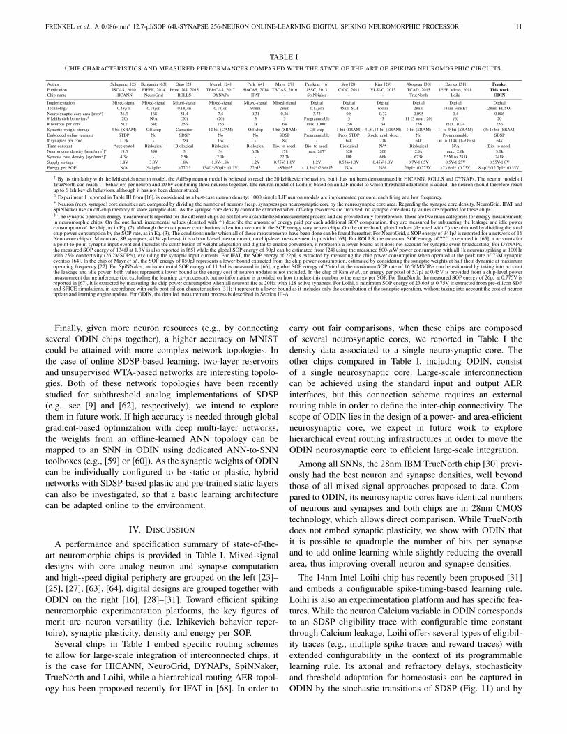
During the inference phase, different coding schemes canbe explored for the weights learned either online with SDSPor offline with SGD, resulting in different tradeoffs betweenaccuracy and energy per inference, as shown in Fig. 15. On theone hand, the rate code is a standard spike coding approach inwhich pixel values are encoded into spike rates [47], the outputneuron that spikes the most defines the inferred class. In this
Energy/inference [nJ]
101 102
Ac
cu
rac
y [
%]
75
80
85
90
online-trained SNN (SDSP)
rank order code
offline-trained SNN (SGD)
rank order code
online-trained SNN (SDSP)
rate code
offline-trained SNN (SGD)
rate code
Fig. 15. Accuracy vs. energy per inference tradeoff for the rank order codeand the rate code on the MNIST dataset. For the rate code, this tradeoffdepends on the character presentation time: the longer the presentation, thehigher the accumulated statistics and the consumed energy. For the rankorder code, the character presentation is stopped as soon as the decision ismade by a single output spike, leading to an efficient spike use. Results areprovided for the ODIN chip using either weights learned off-chip offline withstochastic gradient descent (SGD) or weights learned on-chip online withSDSP, following the setup from Fig. 12.
case, ODIN consumes 404nJ/inference after on-chip learningwith 85% accuracy and 451 nJ/inference after off-chip learningwith 91.9% accuracy. Input characters must be presented fora much longer time than during the on-chip learning phasein order to discriminate characters, sufficient statistics need tobe accumulated in the output neurons. The rate code is thusinefficient in its spike use. On the other hand, the rank ordercode gives a promising approach for a low-power spike codingalternative that is easy to use with LIF neurons [47]. In therank order code, each character is provided to the ODIN SNNas a sequence of successive spikes where no relative timingis involved, each pixel spikes once and all pixels are arrangedin order of decreasing value in the sequence. The sequence isthen presented repeatedly to the ODIN SNN until one outputneuron spikes, this first-spiking neuron defines the inferredclass. In this case, ODIN consumes only 15nJ/inference for84.5% accuracy after on-chip learning (resp. 91.4% accuracyafter off-chip learning), which demonstrates a high efficiency(e.g., see [61] for a review of energy per classification ofpreviously-proposed ANNs, CNNs and SNNs on the original28×28 MNIST dataset). To the best of our knowledge, thisis the first time MNIST classification is demonstrated withon-chip SDSP-based learning. Therefore, Fig. 15 highlightsthat, on the one hand, the SDSP learning rule allows to carryout spiking neural network training on-chip and on-line withlow hardware resources at the cost of a limited accuracydegradation. It corresponds to applications that are constrainedin power and resources both during the training phase and theinference phase and where data is presented on-the-fly to theclassifier (Section I). On the other hand, resorting to the useof an off-chip learning engine is the optimum approach forapplications that are not power- or resource-constrained duringthe training phase: it allows reaching a higher accuracy whilekeeping power efficiency during the inference phase.
FRENKEL et al.: A 0.086-mm2 12.7-pJ/SOP 64k-SYNAPSE 256-NEURON ONLINE-LEARNING DIGITAL SPIKING NEUROMORPHIC PROCESSOR 11
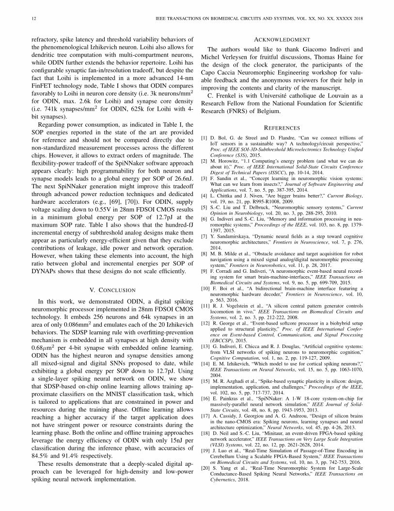
TABLE ICHIP CHARACTERISTICS AND MEASURED PERFORMANCES COMPARED WITH THE STATE OF THE ART OF SPIKING NEUROMORPHIC CIRCUITS.
Author Schemmel [25] Benjamin [63] Qiao [23] Moradi [24] Park [64] Mayr [27] Painkras [16] Seo [28] Kim [29] Akopyan [30] Davies [31] FrenkelPublication ISCAS, 2010 PIEEE, 2014 Front. NS, 2015 TBioCAS, 2017 BioCAS, 2014 TBCAS, 2016 JSSC, 2013 CICC, 2011 VLSI-C, 2015 TCAD, 2015 IEEE Micro, 2018 This workChip name HICANN NeuroGrid ROLLS DYNAPs IFAT - SpiNNaker - - TrueNorth Loihi ODIN
Implementation Mixed-signal Mixed-signal Mixed-signal Mixed-signal Mixed-signal Mixed-signal Digital Digital Digital Digital Digital DigitalTechnology 0.18µm 0.18µm 0.18µm 0.18µm 90nm 28nm 0.13µm 45nm SOI 65nm 28nm 14nm FinFET 28nm FDSOINeurosynaptic core area [mm2] 26.3 168 51.4 7.5 0.31 0.36 3.75 0.8 0.32 0.095 0.4 0.086# Izhikevich behaviors† (20) N/A (20) (20) 3 3 Programmable 3 3 11 (3 neur: 20) (6) 20# neurons per core 512 64k 256 256 2k 64 max. 1000◦ 256 64 256 max. 1024 256Synaptic weight storage 4-bit (SRAM) Off-chip Capacitor 12-bit (CAM) Off-chip 4-bit (SRAM) Off-chip 1-bit (SRAM) 4-,5-,14-bit (SRAM) 1-bit (SRAM) 1- to 9-bit (SRAM) (3+1)-bit (SRAM)Embedded online learning STDP No SDSP No No SDSP Programmable Prob. STDP Stoch. grad. desc. No Programmable SDSP# synapses per core 112k - 128k 16k - 8k - 64k 21k 64k 1M to 114k (1-9 bits) 64kTime constant Accelerated Biological Biological Biological Biological Bio. to accel. Bio. to accel. Biological N/A Biological N/A Bio. to accel.Neuron core density [neur/mm2]∗ 19.5 390 5 34 6.5k 178 max. 267◦ 320 200 2.6k max. 2.6k 3.0kSynapse core density [syn/mm2]∗ 4.3k - 2.5k 2.1k - 22.2k - 80k 66k 673k 2.5M to 285k 741kSupply voltage 1.8V 3.0V 1.8V 1.3V-1.8V 1.2V 0.75V, 1.0V 1.2V 0.53V-1.0V 0.45V-1.0V 0.7V-1.05V 0.5V-1.25V 0.55V-1.0VEnergy per SOP‡ N/A (941pJ)N >77fJM 134fJM/30pJN (1.3V) 22pJN >850pJN >11.3nJM/26.6nJN N/A N/A 26pJN (0.775V) >23.6pJM (0.75V) 8.4pJM/12.7pJN (0.55V)
† By its similarity with the Izhikevich neuron model, the AdExp neuron model is believed to reach the 20 Izhikevich behaviors, but it has not been demonstrated in HICANN, ROLLS and DYNAPs. The neuron model ofTrueNorth can reach 11 behaviors per neuron and 20 by combining three neurons together. The neuron model of Loihi is based on an LIF model to which threshold adaptation is added: the neuron should therefore reachup to 6 Izhikevich behaviors, although it has not been demonstrated.◦ Experiment 1 reported in Table III from [16], is considered as a best-case neuron density: 1000 simple LIF neuron models are implemented per core, each firing at a low frequency.∗ Neuron (resp. synapse) core densities are computed by dividing the number of neurons (resp. synapses) per neurosynaptic core by the neurosynaptic core area. Regarding the synapse core density, NeuroGrid, IFAT andSpiNNaker use an off-chip memory to store synaptic data. As the synapse core density cannot be extracted when off-chip resources are involved, no synapse core density values are reported for these chips.‡ The synaptic operation energy measurements reported for the different chips do not follow a standardized measurement process and are provided only for reference. There are two main categories for energy measurementsin neuromorphic chips. On the one hand, incremental values (denoted with M) describe the amount of energy paid per each additional SOP computation, they are measured by subtracting the leakage and idle powerconsumption of the chip, as in Eq. (2), although the exact power contributions taken into account in the SOP energy vary across chips. On the other hand, global values (denoted with N) are obtained by dividing the totalchip power consumption by the SOP rate, as in Eq. (3). The conditions under which all of these measurements have been done can be found hereafter. For NeuroGrid, a SOP energy of 941pJ is reported for a network of 16Neurocore chips (1M neurons, 8B synapses, 413k spikes/s): it is a board-level measurement, no chip-level measurement is provided [63]. For ROLLS, the measured SOP energy of 77fJ is reported in [65], it accounts fora point-to-point synaptic input event and includes the contribution of weight adaptation and digital-to-analog conversion, it represents a lower bound as it does not account for synaptic event broadcasting. For DYNAPs,the measured SOP energy of 134fJ at 1.3V is also reported in [65] while the global SOP energy of 30pJ can be estimated from [24] using the measured 800-µW power consumption with all 1k neurons spiking at 100Hzwith 25% connectivity (26.2MSOP/s), excluding the synaptic input currents. For IFAT, the SOP energy of 22pJ is extracted by measuring the chip power consumption when operated at the peak rate of 73M synapticevents/s [64]. In the chip of Mayr et al., the SOP energy of 850pJ represents a lower bound extracted from the chip power consumption, estimated by considering the synaptic weights at half their dynamic at maximumoperating frequency [27]. For SpiNNaker, an incremental SOP energy of 11.3nJ is measured in [66], a global SOP energy of 26.6nJ at the maximum SOP rate of 16.56MSOP/s can be estimated by taking into accountthe leakage and idle power; both values represent a lower bound as the energy cost of neuron updates is not included. In the chip of Kim et al., an energy per pixel of 5.7pJ at 0.45V is provided from a chip-level powermeasurement during inference (i.e. excluding the learning co-processor), but no information is provided on how to relate this number to the energy per SOP. For TrueNorth, the measured SOP energy of 26pJ at 0.775V isreported in [67], it is extracted by measuring the chip power consumption when all neurons fire at 20Hz with 128 active synapses. For Loihi, a minimum SOP energy of 23.6pJ at 0.75V is extracted from pre-silicon SDFand SPICE simulations, in accordance with early post-silicon characterization [31]; it represents a lower bound as it includes only the contribution of the synaptic operation, without taking into account the cost of neuronupdate and learning engine update. For ODIN, the detailed measurement process is described in Section III-A.
Finally, given more neuron resources (e.g., by connectingseveral ODIN chips together), a higher accuracy on MNISTcould be attained with more complex network topologies. Inthe case of online SDSP-based learning, two-layer reservoirsand unsupervised WTA-based networks are interesting topolo-gies. Both of these network topologies have been recentlystudied for subthreshold analog implementations of SDSP(e.g., see [9] and [62], respectively), we intend to explorethem in future work. If high accuracy is needed through globalgradient-based optimization with deep multi-layer networks,the weights from an offline-learned ANN topology can bemapped to an SNN in ODIN using dedicated ANN-to-SNNtoolboxes (e.g., [59] or [60]). As the synaptic weights of ODINcan be individually configured to be static or plastic, hybridnetworks with SDSP-based plastic and pre-trained static layerscan also be investigated, so that a basic learning architecturecan be adapted online to the environment.
IV. DISCUSSION
A performance and specification summary of state-of-the-art neuromorphic chips is provided in Table I. Mixed-signaldesigns with core analog neuron and synapse computationand high-speed digital periphery are grouped on the left [23]–[25], [27], [63], [64], digital designs are grouped together withODIN on the right [16], [28]–[31]. Toward efficient spikingneuromorphic experimentation platforms, the key figures ofmerit are neuron versatility (i.e. Izhikevich behavior reper-toire), synaptic plasticity, density and energy per SOP.
Several chips in Table I embed specific routing schemesto allow for large-scale integration of interconnected chips, itis the case for HICANN, NeuroGrid, DYNAPs, SpiNNaker,TrueNorth and Loihi, while a hierarchical routing AER topol-ogy has been proposed recently for IFAT in [68]. In order to
carry out fair comparisons, when these chips are composedof several neurosynaptic cores, we reported in Table I thedensity data associated to a single neurosynaptic core. Theother chips compared in Table I, including ODIN, consistof a single neurosynaptic core. Large-scale interconnectioncan be achieved using the standard input and output AERinterfaces, but this connection scheme requires an externalrouting table in order to define the inter-chip connectivity. Thescope of ODIN lies in the design of a power- and area-efficientneurosynaptic core, we expect in future work to explorehierarchical event routing infrastructures in order to move theODIN neurosynaptic core to efficient large-scale integration.
Among all SNNs, the 28nm IBM TrueNorth chip [30] previ-ously had the best neuron and synapse densities, well beyondthose of all mixed-signal approaches proposed to date. Com-pared to ODIN, its neurosynaptic cores have identical numbersof neurons and synapses and both chips are in 28nm CMOStechnology, which allows direct comparison. While TrueNorthdoes not embed synaptic plasticity, we show with ODIN thatit is possible to quadruple the number of bits per synapseand to add online learning while slightly reducing the overallarea, thus improving overall neuron and synapse densities.
The 14nm Intel Loihi chip has recently been proposed [31]and embeds a configurable spike-timing-based learning rule.Loihi is also an experimentation platform and has specific fea-tures. While the neuron Calcium variable in ODIN correspondsto an SDSP eligibility trace with configurable time constantthrough Calcium leakage, Loihi offers several types of eligibil-ity traces (e.g., multiple spike traces and reward traces) withextended configurability in the context of its programmablelearning rule. Its axonal and refractory delays, stochasticityand threshold adaptation for homeostasis can be captured inODIN by the stochastic transitions of SDSP (Fig. 11) and by
12 IEEE TRANSACTIONS ON BIOMEDICAL CIRCUITS AND SYSTEMS, VOL. XX, NO. XX, XXXXX 2018
refractory, spike latency and threshold variability behaviors ofthe phenomenological Izhikevich neuron. Loihi also allows fordendritic tree computation with multi-compartment neurons,while ODIN further extends the behavior repertoire. Loihi hasconfigurable synaptic fan-in/resolution tradeoff, but despite thefact that Loihi is implemented in a more advanced 14-nmFinFET technology node, Table I shows that ODIN comparesfavorably to Loihi in neuron core density (i.e. 3k neurons/mm2
for ODIN, max. 2.6k for Loihi) and synapse core density(i.e. 741k synapses/mm2 for ODIN, 625k for Loihi with 4-bit synapses).
Regarding power consumption, as indicated in Table I, theSOP energies reported in the state of the art are providedfor reference and should not be compared directly due tonon-standardized measurement processes across the differentchips. However, it allows to extract orders of magnitude. Theflexibility-power tradeoff of the SpiNNaker software approachappears clearly: high programmability for both neuron andsynapse models leads to a global energy per SOP of 26.6nJ.The next SpiNNaker generation might improve this tradeoffthrough advanced power reduction techniques and dedicatedhardware accelerators (e.g., [69], [70]). For ODIN, supplyvoltage scaling down to 0.55V in 28nm FDSOI CMOS resultsin a minimum global energy per SOP of 12.7pJ at themaximum SOP rate. Table I also shows that the hundred-fJincremental energy of subthreshold analog designs make themappear as particularly energy-efficient given that they excludecontributions of leakage, idle power and network operation.However, when taking these elements into account, the highratio between global and incremental energies per SOP ofDYNAPs shows that these designs do not scale efficiently.
V. CONCLUSION
In this work, we demonstrated ODIN, a digital spikingneuromorphic processor implemented in 28nm FDSOI CMOStechnology. It embeds 256 neurons and 64k synapses in anarea of only 0.086mm2 and emulates each of the 20 Izhikevichbehaviors. The SDSP learning rule with overfitting-preventionmechanism is embedded in all synapses at high density with0.68µm2 per 4-bit synapse with embedded online learning.ODIN has the highest neuron and synapse densities amongall mixed-signal and digital SNNs proposed to date, whileexhibiting a global energy per SOP down to 12.7pJ. Usinga single-layer spiking neural network on ODIN, we showthat SDSP-based on-chip online learning allows training ap-proximate classifiers on the MNIST classification task, whichis tailored to applications that are constrained in power andresources during the training phase. Offline learning allowsreaching a higher accuracy if the target application doesnot have stringent power or resource constraints during thelearning phase. Both the online and offline training approachesleverage the energy efficiency of ODIN with only 15nJ perclassification during the inference phase, with accuracies of84.5% and 91.4% respectively.
These results demonstrate that a deeply-scaled digital ap-proach can be leveraged for high-density and low-powerspiking neural network implementation.
ACKNOWLEDGMENT
The authors would like to thank Giacomo Indiveri andMichel Verleysen for fruitful discussions, Thomas Haine forthe design of the clock generator, the participants of theCapo Caccia Neuromorphic Engineering workshop for valu-able feedback and the anonymous reviewers for their help inimproving the contents and clarity of the manuscript.
C. Frenkel is with Universite catholique de Louvain as aResearch Fellow from the National Foundation for ScientificResearch (FNRS) of Belgium.
REFERENCES
[1] D. Bol, G. de Streel and D. Flandre, “Can we connect trillions ofIoT sensors in a sustainable way? A technology/circuit perspective,”Proc. of IEEE SOI-3D-Subthreshold Microelectronics Technology UnifiedConference (S3S), 2015.
[2] M. Horowitz, “1.1 Computing’s energy problem (and what we can doabout it),” Proc. of IEEE International Solid-State Circuits ConferenceDigest of Technical Papers (ISSCC), pp. 10-14, 2014.
[3] F. Sandin et al., “Concept learning in neuromorphic vision systems:What can we learn from insects?,” Journal of Software Engineering andApplications, vol. 7, no. 5, pp. 387-395, 2014.
[4] L. Chittka and J. Niven, “Are bigger brains better?,” Current Biology,vol. 19, no. 21, pp. R995-R1008, 2009.
[5] S.-C. Liu and T. Delbruck, “Neuromorphic sensory systems,” CurrentOpinion in Neurobiology, vol. 20, no. 3, pp. 288-295, 2010.
[6] G. Indiveri and S.-C. Liu, “Memory and information processing in neu-romorphic systems,” Proceedings of the IEEE, vol. 103, no. 8, pp. 1379-1397, 2015.
[7] Y. Sandamirskaya, “Dynamic neural fields as a step toward cognitiveneuromorphic architectures,” Frontiers in Neuroscience, vol. 7, p. 276,2014.
[8] M. B. Milde et al., “Obstacle avoidance and target acquisition for robotnavigation using a mixed signal analog/digital neuromorphic processingsystem,” Frontiers in Neurorobotics, vol. 11, p. 28, 2017.
[9] F. Corradi and G. Indiveri, “A neuromorphic event-based neural record-ing system for smart brain-machine-interfaces,” IEEE Transactions onBiomedical Circuits and Systems, vol. 9, no. 5, pp. 699-709, 2015.
[10] F. Boi et al., “A bidirectional brain-machine interface featuring aneuromorphic hardware decoder,” Frontiers in Neuroscience, vol. 10,p. 563, 2016.
[11] R. J. Vogelstein et al., “A silicon central pattern generator controlslocomotion in vivo,” IEEE Transactions on Biomedical Circuits andSystems, vol. 2, no. 3, pp. 212-222, 2008.
[12] R. George et al., “Event-based softcore processor in a biohybrid setupapplied to structural plasticity,” Proc. of IEEE International Confer-ence on Event-based Control, Communication, and Signal Processing(EBCCSP), 2015.
[13] G. Indiveri, E. Chicca and R. J. Douglas, “Artificial cognitive systems:from VLSI networks of spiking neurons to neuromorphic cognition,”Cognitive Computation, vol. 1, no. 2, pp. 119-127, 2009.
[14] E. M. Izhikevich, “Which model to use for cortical spiking neurons?,”IEEE Transactions on Neural Networks, vol. 15, no. 5, pp. 1063-1070,2004.
[15] M. R. Azghadi et al., “Spike-based synaptic plasticity in silicon: design,implementation, application, and challenges,” Proceedings of the IEEE,vol. 102, no. 5, pp. 717-737, 2014.
[16] E. Painkras et al., “SpiNNaker: A 1-W 18-core system-on-chip formassively-parallel neural network simulation,” IEEE Journal of Solid-State Circuits, vol. 48, no. 8, pp. 1943-1953, 2013.
[17] A. Cassidy, J. Georgiou and A. G. Andreou, “Design of silicon brainsin the nano-CMOS era: Spiking neurons, learning synapses and neuralarchitecture optimization,” Neural Networks, vol. 45, pp. 4-26, 2013.
[18] D. Neil and S.-C. Liu, “Minitaur, an event-driven FPGA-based spikingnetwork accelerator,” IEEE Transactions on Very Large Scale Integration(VLSI) Systems, vol. 22, no. 12, pp. 2621-2628, 2014.
[19] J. Luo et al., “Real-Time Simulation of Passage-of-Time Encoding inCerebellum Using a Scalable FPGA-Based System,” IEEE Transactionson Biomedical Circuits and Systems, vol. 10, no. 3, pp. 742-753, 2016.
[20] S. Yang et al., “Real-Time Neuromorphic System for Large-ScaleConductance-Based Spiking Neural Networks,” IEEE Transactions onCybernetics, 2018.
FRENKEL et al.: A 0.086-mm2 12.7-pJ/SOP 64k-SYNAPSE 256-NEURON ONLINE-LEARNING DIGITAL SPIKING NEUROMORPHIC PROCESSOR 13
[21] C. S. Poon and K. Zhou, “Neuromorphic silicon neurons and large-scaleneural networks: challenges and opportunities,” Frontiers in Neuroscience,vol. 5, p. 108, 2011.
[22] C. Mead, Analog VLSI and Neural Systems. Reading, MA: Addison-Wesley, 1989.
[23] N. Qiao et al., “A reconfigurable on-line learning spiking neuromorphicprocessor comprising 256 neurons and 128K synapses,” Frontiers inNeuroscience, vol. 9, no. 141, 2015.
[24] S. Moradi et al., “A scalable multicore architecture with heterogeneousmemory structures for Dynamic Neuromorphic Asynchronous Processors(DYNAPs),” IEEE Transactions on Biomedical Circuits and Systems,vol. 12, no. 1, pp. 106-122, 2017.
[25] J. Schemmel et al., “A wafer-scale neuromorphic hardware system forlarge-scale neural modeling,” Proc. of IEEE International Symposium onCircuits and Systems (ISCAS), pp. 1947-1950, 2010.
[26] M. Noack et al., “Switched-capacitor realization of presynaptic short-term-plasticity and stop-learning synapses in 28 nm CMOS,” Frontiers inneuroscience, vol. 9, p. 10, 2015.
[27] C. Mayr et al., “A biological-realtime neuromorphic system in 28 nmCMOS using low-leakage switched capacitor circuits,” IEEE Transactionson Biomedical Circuits and Systems, vol. 10, no. 1, pp. 243-254, 2016.
[28] J.-S. Seo et al., “A 45nm CMOS neuromorphic chip with a scalablearchitecture for learning in networks of spiking neurons,” Proc. of IEEECustom Integrated Circuits Conference (CICC), 2011.
[29] J. K. Kim et al., “A 640M pixel/s 3.65 mW sparse event-drivenneuromorphic object recognition processor with on-chip learning,” IEEESymposium on VLSI Circuits (VLSI-C), pp. C50-C51, 2015.
[30] F. Akopyan et al., “TrueNorth: Design and tool flow of a 65 mW 1million neuron programmable neurosynaptic chip,” IEEE Transactionson Computer-Aided Design of Integrated Circuits and Systems, vol. 34,no. 10, pp. 1537-1557, 2015.
[31] M. Davies et al., “Loihi: A neuromorphic manycore processor with on-chip learning,” IEEE Micro, vol. 38, no. 1, pp. 82-99, 2018.
[32] H. Markram, W. Gerstner and P. J. Sjostrom, “Spike-timing-dependentplasticity: a comprehensive overview,” Frontiers in Synaptic Neuro-science, vol. 4, no. 2, 2012.
[33] J. M. Brader, W. Senn and S. Fusi, “Learning real-world stimuli in aneural network with spike-driven synaptic dynamics,” Neural Computa-tion, vol. 19, no. 11, pp. 2881-2912, 2007.
[34] C. Frenkel et al., “A fully-synthesized 20-gate digital spike-basedsynapse with embedded online learning,” Proc. of IEEE InternationalSymposium on Circuits and Systems (ISCAS), pp. 17-20, 2017.
[35] P. Lin, S. Pi and Q. Xia, “3D integration of planar crossbar memris-tive devices with CMOS substrate,” Nanotechnology, vol. 25, no. 40,ID 405202, 2014.
[36] J. Rofeh et al., “Vertical integration of memristors onto foundry CMOSdies using wafer-scale integration,” Proc. of IEEE Electronic Componentsand Technology Conference (ECTC), pp. 957-962, 2015.
[37] G. Indiveri, F. Stefanini and E. Chicca, “Spike-based learning with ageneralized integrate and fire silicon neuron,” Proc. of IEEE InternationalSymposium on Circuits and Systems (ISCAS), pp. 1951-1954, 2010.
[38] A. L. Hodgkin and A. F. Huxley, “A quantitative description of mem-brane current and its application to conduction and excitation in nerve,”Journal of Physiology, vol. 117, no. 4, pp. 500-544, 1952.
[39] E. M. Izhikevich, “Simple model of spiking neurons,” IEEE Transactionson Neural Networks, vol. 14, no. 6, pp. 1569-1572, 2003.
[40] R. Brette and W. Gerstner, “Adaptive exponential integrate-and-firemodel as an effective description of neuronal activity,” Journal of Neu-rophysiology, vol. 94, no. 5, pp. 3637-3642, 2005.
[41] Y. LeCun and C. Cortes, “The MNIST database of handwritten digits,”1998 [Online]. Available: http://yann.lecun.com/exdb/mnist/.
[42] A. Mortara and E. A. Vittoz, “A communication architecture tailoredfor analog VLSI artificial neural networks: intrinsic performance andlimitations,” IEEE Transactions on Neural Networks, vol. 5, no. 3,pp. 459-466, 1994.
[43] K. A. Boahen, “Point-to-point connectivity between neuromorphic chipsusing address events,” IEEE Transactions on Circuits and Systems II,vol. 47, no. 5, pp. 416-434, 2000.
[44] A. Cassidy, A. G. Andreou and J. Georgiou, “A combinational digitallogic approach to STDP,” Proc. of IEEE International Symposium ofCircuits and Systems (ISCAS), pp. 673-676, 2011.
[45] G. Chen et al., “A dense 45nm half-differential SRAM with lowerminimum operating voltage,” IEEE International Symposium on Circuitsand Systems (ISCAS), pp. 57-60, 2011.
[46] J. V. Arthur and K. Boahen, “Learning in silicon: Timing is everything,”Proc. of Advances in Neural Information Processing Systems (NIPS),pp. 75-82, 2006.
[47] S. Thorpe, A. Delorme and R. Van Rullen, “Spike-based strategies forrapid processing,” Neural Networks, vol. 14, no. 6-7, pp. 715-725, 2001.
[48] Q. Yu, et al., “Rapid feedforward computation by temporal encoding andlearning with spiking neurons,” IEEE Transactions on Neural Networksand Learning Systems, vol. 24, no. 10, pp. 1539-1552, 2013.
[49] N. Qiao, C. Bartolozzi and G. Indiveri, “An ultralow leakage synapticscaling homeostatic plasticity circuit with configurable time scales up to100 ks,” IEEE Transactions on Biomedical Circuits and Systems, vol. 11,no. 6, pp. 1271-1277, 2017.
[50] S. Sheik, E. Chicca and G. Indiveri, “Exploiting device mismatch inneuromorphic VLSI systems to implement axonal delays,” Proc. of IEEEInternational Joint Conference on Neural Networks (IJCNN), 2012.
[51] C. Frenkel, J.-D. Legat and D. Bol, “A compact phenomenologicaldigital neuron implementing the 20 Izhikevich behaviors,” Proc. of IEEEBiomedical Circuits and Systems Conference (BioCAS), pp. 677-680,2017.
[52] H. Soleimani, A. Ahmadi and M. Bavandpour, “Biologically inspiredspiking neurons: Piecewise linear models and digital implementation,”IEEE Transactions on Circuits and Systems I: Regular Papers, vol. 59,no. 12, pp. 2991-3004, 2012.
[53] S. Yang et al., “Cost-efficient FPGA implementation of basal gangliaand their Parkinsonian analysis,” Neural Networks, vol. 71, pp. 62-75,2015.
[54] E. Neftci et al., “Synthesizing cognition in neuromorphic electronicsystems,” Proceedings of the National Academy of Sciences, vol. 110,no. 37, pp. E3468-E3476, 2013.
[55] C. Koch, Biophysics of computation: information processing in singleneurons, Oxford university press, 1999.
[56] S.-W. Moon, J. Rexford and K. G. Shin, “Scalable hardware priorityqueue architectures for high-speed packet switches,” IEEE Transactionson Computers, vol. 49, no. 11, pp. 1215-1227, 2000.
[57] M. Courbariaux et al., “Binarized neural networks: Training deep neuralnetworks with weights and activations constrained to +1 or -1,” arXivpreprint arXiv:1602.02830, 2016.
[58] B. Moons et al., “Minimum energy quantized neural networks,” arXivpreprint arXiv:1711.00215, 2017.
[59] B. Rueckauer et al., “Conversion of continuous-valued deep networksto efficient event-driven networks for image classification,” Frontiers inNeuroscience, vol. 11, p. 682, 2017.
[60] P. U. Diehl et al., “Fast-classifying, high-accuracy spiking deep networksthrough weight and threshold balancing,” Proc. of International JointConference on Neural Networks (IJCNN), 2015.
[61] P. N. Whatmough et al., “A 28nm SoC with a 1.2 GHz 568nJ/predictionsparse deep-neural-network engine with >0.1 timing error rate tolerancefor IoT applications,” Proc. of IEEE International Solid-State CircuitsConference (ISSCC), 2017.
[62] R. Kreiser et al., “On-chip unsupervised learning in winner-take-allnetworks of spiking neurons,” Proc. of IEEE Biomedical Circuits andSystems Conference (BioCAS), pp. 424-427, 2017.
[63] B. V. Benjamin et al., “Neurogrid: A mixed-analog-digital multichipsystem for large-scale neural simulations,” Proceedings of the IEEE,vol. 102, no. 5, pp. 699-716, 2014.
[64] J. Park et al., “A 65k-neuron 73-Mevents/s 22-pJ/event asynchronousmicro-pipelined integrate-and-fire array transceiver,” Proc. of IEEEBiomedical Circuits and Systems Conference (BioCAS), 2014.
[65] G. Indiveri, F. Corradi and N. Qiao, “Neuromorphic architectures forspiking deep neural networks,” Proc. of IEEE Electron Devices Meeting(IEDM), 2015.
[66] E. Stromatias et al., “Scalable energy-efficient, low-latency implemen-tations of trained spiking deep belief networks on SpiNNaker,” Proc. ofIEEE International Joint Conference on Neural Networks (IJCNN), 2015.
[67] P. A. Merolla et al., “A million spiking-neuron integrated circuit witha scalable communication network and interface,” Science, vol. 345,no. 6197, pp. 668-673, 2014.
[68] J. Park et al., “Hierarchical address event routing for reconfigurablelarge-scale neuromorphic systems,” IEEE Transactions on Neural Net-works and Learning Systems, vol. 28, no. 10, pp. 2408-2422, 2017.
[69] S. Hoppner et al., “Dynamic voltage and frequency scaling for neuro-morphic many-core systems,” IEEE International Symposium on Circuitsand Systems (ISCAS), 2017.
[70] J. Partzsch et al., “A fixed point exponential function accelerator for aneuromorphic many-core system,” Proc. of IEEE International Sympo-sium on Circuits and Systems (ISCAS), 2017.
14 IEEE TRANSACTIONS ON BIOMEDICAL CIRCUITS AND SYSTEMS, VOL. XX, NO. XX, XXXXX 2018
Charlotte Frenkel (S’15) received the M.Sc. de-gree (summa cum laude) in Electromechanical En-gineering from Universite catholique de Louvain(UCL), Louvain-la-Neuve, Belgium, in 2015. Sheis currently working toward the Ph.D. degree asa Research Fellow of the National Foundation forScientific Research (FNRS) of Belgium, under thesupervision of Prof. D. Bol and Prof. J.-D. Legat.
Her current research focuses on the design oflow-power and high-density neuromorphic circuitsas efficient non-von Neumann architectures for real-
time recognition and online learning.Ms. Frenkel serves as a reviewer for the IEEE Transactions on Neural
Networks and Learning Systems journal and for IEEE S3S, ISCAS andBioCAS conferences.
Martin Lefebvre (S’17) received the M.Sc. de-gree (summa cum laude) in electromechanical engi-neering from the Universite catholique de Louvain(UCL), Louvain-la-Neuve, Belgium, in 2017, wherehe is currently pursuing the Ph.D. degree, under thesupervision of Prof. D. Bol and Prof. L. Jacques.
His current research interests include the designof low-power mixed-signal circuits as efficient hard-ware implementations for machine learning and im-age processing algorithms.
Jean-Didier Legat (S’79-M’85-SM’17) received hisengineering and PhD degrees in microelectronicsfrom the Universite catholique de Louvain, Louvain-la-Neuve, Belgium in 1981 and 1987, respectively.
From 1987 to 1990, he was with Image Recog-nition Integrated Systems (I.R.I.S.), a new companyspecialised in optical character recognition and auto-matic document processing. Jean-Didier Legat wasco-founder and Vice-President of I.R.I.S. In October1990, he came back to the UCL MicroelectronicsLaboratory. He is presently full Professor. From
2003 to 2008, he was the Dean of the Louvain School of Engineering.Currently, he is Senior Advisor to the President for Technology Transfer andHead of the ICTEAM Research Institute. His current interests are processorarchitecture, low-power digital integrated circuit, real-time embedded systems,mixed-signal design and hardware-software codesign for reconfigurable sys-tems. He has been an author or co-author of more than 200 publications inthe field of microelectronics, low-power digital circuits, computer architecture,digital signal processing, computer vision and pattern recognition.
David Bol (S’07-M’09-SM’18) received the M.Sc.degree in Electromechanical Engineering and thePh.D degree in Engineering Science from Universitecatholique de Louvain (UCL), Louvain-la-Neuve,Belgium in 2004 and 2008, respectively. In 2005,he was a visiting Ph.D student at the CNM Na-tional Centre for Microelectronics, Sevilla, Spain,in advanced logic design. In 2009, he was a post-doctoral researcher at intoPIX, Louvain-la-Neuve,Belgium, in low-power design for JPEG2000 imageprocessing. In 2010, he was a visiting postdoctoral
researcher at the UC Berkeley Laboratory for Manufacturing and Sustainabil-ity, Berkeley, CA, in life-cycle assessment of the semiconductor environmentalimpact. He is now an assistant professor at UCL. In 2015, he participated tothe creation of e-peas semiconductors, Louvain-la-Neuve, Belgium.
Prof. Bol leads with Prof. Denis Flandre the Electronic Circuits andSystems (ECS) research group focused on ultra-low-power design of inte-grated circuits for the IoT including computing, power management, sensingand RF communications with focuses on technology/circuit interaction innanometer CMOS nodes, variability mitigation, mixed-signal SoC architectureand implementation. He gives four M.Sc. courses in Electrical Engineering atUCL on digital, analog and mixed-signal integrated circuits and systems aswell as sensors.
Prof. Bol has authored or co-authored more than 100 technical papers andconference contributions and holds three delivered patents. He (co-)receivedthree Best Paper/Poster/Design Awards in IEEE conferences (ICCD 2008,SOI Conf. 2008, FTFC 2014). He also serves as an editor for MDPI J. Low-Power Electronics and Applications, as a TPC member of IEEE SubVt/S3Sconference and as a reviewer for various journals and conferences such asIEEE J. of Solid-State Circuits, IEEE Trans. on VLSI Syst., IEEE Trans. onCircuits and Syst. I/II. Since 2008, he presented several invited papers andkeynote tutorials in international conferences including a forum presentationat IEEE ISSCC 2018.