Embed Size (px)
Citation preview
This article has been accepted for inclusion in a future issue of this journal. Content is final as presented, with the exception of pagination.
IEEE TRANSACTIONS ON ELECTRON DEVICES 1
Impact of Ground Plane Doping and Bottom-Gate Biasing on Electrical Properties inIn0.53Ga0.47As-OI MOSFETs and DonorWafer Reusability Toward Monolithic 3-DIntegration With In0.53Ga0.47As Channel
Seong Kwang Kim, Jae-Phil Shim , Dae-Myeong Geum, Jaewon Kim, Chang Zoo Kim, Han-Sung Kim,Jin Dong Song, Sung-Jin Choi , Dae Hwan Kim , Senior Member, IEEE, Won Jun Choi,
Hyung-Jun Kim, Dong Myong Kim , and Sanghyeon Kim , Member, IEEE
Abstract— In this paper, we fabricated In0.53Ga0.47As-oninsulator (OI) MOSFETs on Si substrates with different dop-ing types to mimic ground plane doping using direct waferbonding and epitaxial lift-off (ELO) techniques. We investi-gated the impact of doping types on the ground plane andthe backgate biasing, which are important and preferablecomponents in monolithic 3-D (M3D) integration, on theelectrical properties of MOSFETs, such as the threshold
Manuscript received January 21, 2018; accepted February 22, 2018.This work was supported in part by the National Research Foundation ofKorea (NRF) grant through the Korean Government (MSIP) under Grant2016R1A5A1012966 and Grant 2017R1A2B4007820, in part by NRFunder Grant 2015004870 and Grant 2016910562, in part by the KISTInstitutional Program under Grant 2E27160, KIST, South Korea, andin part by the Future Semiconductor Device Technology DevelopmentProgram through the Ministry of Trade, Industry and Energy under Grant10052962. The review of this paper was arranged by Editor M. S. Bakir.(Corresponding authors: Dong Myong Kim; Sanghyeon Kim.)
S. K. Kim, J. D. Song, and W. J. Choi are with the Center forOpto-Electronic Materials and Devices, Korea Institute of Science andTechnology, Seoul 02792, South Korea.
J.-P. Shim is with the Center for Spintronics, Korea Institute of Scienceand Technology, Seoul 02792, South Korea.
D.-M. Geum is with the Center for Opto-Electronic Materials andDevices, Korea Institute of Science and Technology, Seoul 02792,South Korea, and also with the Department of Materials Science andEngineering, Seoul National University, Seoul 151-742, South Korea.
J. Kim, S.-J. Choi, D. H. Kim, and D. M. Kim are with Kookmin University,Seoul 02707, South Korea (e-mail: [email protected]).
C. Z. Kim is with the Korea Advanced Nano Fab Center, Suwon 443-766, South Korea.
H.-S. Kim is with the Center for Spintronics, Korea Institute of Scienceand Technology, Seoul 02792, South Korea, and also with the KU-KISTGraduate School of Converging Science and Technology, Seoul 136-791,South Korea.
H.-J. Kim is with the Center for Spintronics, Korea Institute of Scienceand Technology, Seoul 02792, South Korea, and also with the Divisionof Nano and Information Technology, Korea Institute of Science andTechnology School, Korea University of Science and Technology, Seoul02792, South Korea.
S. Kim is with the Center for Opto-Electronic Materials and Devices,Korea Institute of Science and Technology, Seoul 02792, South Korea,and also with the Division of Nano and Information Technology, KoreaInstitute of Science and Technology School, Korea University of Scienceand Technology, Seoul 02792, South Korea (e-mail: [email protected])
Color versions of one or more of the figures in this paper are availableonline at http://ieeexplore.ieee.org.
Digital Object Identifier 10.1109/TED.2018.2810304
voltage (V T) and the effective mobility (µeff). It was foundthat V T and µeff were significantly modulated by the back-substrate doping and the backbiasing. These observationswere explained by the change of carrier distributions, whichwere confirmed by technology computer-aided design sim-ulation. Furthermore, we investigated the reusability of InPdonor substrates for sequential epitaxial growth after ELOprocess toward a cost-effective M3D integration with theIn0.53Ga0.47As channel.
Index Terms— III–V, compound semiconductor, epitaxiallift-off (ELO), InGaAs, InGaAs-OI, monolithic 3-D (M3D),MOSFETs, wafer bonding, wafer reuse.
I. INTRODUCTION
MONOLITHIC 3-D (M3D) integration has receivedmuch attention from the industry as well as academia
due to their benefits in high integration density of devicesand the reduction of power consumption via vertical devicestacking [1]–[3]. Moreover, an interconnection delay canbe reduced by minimizing the resistance of interconnectionwires [4]. On the other hand, in terms of the fabricationprocess for the M3D integration, a low-temperature processingis necessary to fabricate devices to protect bottom devicesduring the fabrication of top devices. From this aspect, highmobility channels, such as III–V compound semiconductorsand Ge, have a strong advantage, because processing tem-perature for them is typically lower than 400 °C [4]–[10].Among III–V compound semiconductors, InGaAs has beenactively studied as a channel material for n-FETs of the nextnode logic applications, because InGaAs has quite attractivecharacteristics of high effective mobility and injection velocitythan those of silicon [8]–[18]. There are several methods forstacking the InGaAs channel toward the M3D integration,such as the direct epitaxial growth, the aspect ratio trapping,the confined epitaxial lateral overgrowth, and the direct waferbonding (DWB) [6]–[12], [14], [16]–[18]. Among these meth-ods, the DWB using an oxide bonding material is the moststraightforward and the best way to stack high-quality films atlow process temperature for M3D, because the epitaxy-based
0018-9383 © 2018 IEEE. Personal use is permitted, but republication/redistribution requires IEEE permission.See http://www.ieee.org/publications_standards/publications/rights/index.html for more information.
This article has been accepted for inclusion in a future issue of this journal. Content is final as presented, with the exception of pagination.2 IEEE TRANSACTIONS ON ELECTRON DEVICES
Fig. 1. Schematic of M3D integration with the InGaAs channel andits stacking flow. The proposed integration concept includes the groundplane and the metal plate in ILD for VT control and the use of DWB/ELO)for donor wafer reuse.
method needs high process temperature, typically over 500 °C,during the growth of the channel layer. Fig. 1 shows theschematic of M3D integration with the InGaAs channel andits stacking flow of the DWB and the epitaxial lift-off (ELO)with a donor-wafer recycling.
A stacked structure by oxide bonding naturally has abackgate structure of the metal plate and the doped groundplane in top-level device (>2nd tier) and bottom-level device,respectively. As observed in SOI devices, a ground planeplays an important role in the control of the short-channeleffect, the mobility, and the threshold voltage (VT ) inMOSFETs [19]–[21]. However, there are quite limited studieson these issues in InGaAs-OI MOSFETs [22]. Here, the metalplates patterned in the interlayer dielectric (ILD) seem toaffect the wafer bonding, but the wafer with an additionaloxide can be used for sequential wafer bonding after surfaceplanarization. Moreover, hybrid bonding with a mixed patternof metal and also oxide can be the viable solution to fabricatestacked structure even for higher tier device layers (second tierand above).
On the other hand, to explore M3D with the InGaAschannel, cost issues are quite problematic, because III–Vsubstrate is typically more expensive than Si. Therefore,the M3D process design with the InGaAs channel must takeaccount of the integration route for the process cost reduction.
In this paper, we demonstrated InGaAs-OI MOSFETs onSi substrates with different doping types to mimic the groundplane doping using the DWB and the ELO process [7]–[10].We systematically investigated the impact of the ground planedoping and the backgate bias on the electrical characteristics.Furthermore, we investigated the wafer reusability of theInP donor wafer after the ELO process for a cost-effectiveM3D integration.
II. FABRICATION OF In0.53Ga0.47As-OI MOSFETS
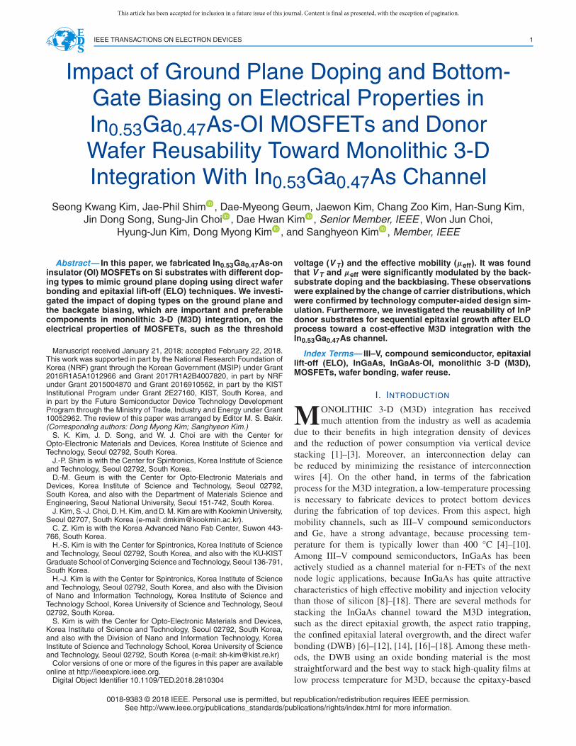
Fig. 2(a) shows a schematic of the device structureand the fabrication process flow. To fabricate In0.53Ga0.47As-OI MOSFETs, first, we fabricated In0.53Ga0.47As-OI wafervia the DWB and the ELO processes [7]. Device layerswere composed of a 20-nm-thick In0.53Ga0.47As chan-nel [unintentionally doped (UID)], a 5-nm-thick InP etchstop (UID), and a 50-nm-thick n+ In0.53Ga0.47As contact
Fig. 2. (a) Schematic of the device structure and fabricationprocess of In0.53Ga0.47As-OI MOSFETs. (b) Cross-sectional TEMimage of In0.53Ga0.47As-OI MOSFETs. (c) High-resolution cross-sectional TEM image of In0.53Ga0.47As region. (d) EDX mapping profileof In0.53Ga0.47As-OI MOSFETs.
layer (ND ∼ 1 × 1019 cm−3) from the bottom side. In thispaper, we used a channel thickness of 20 nm, but a thinnerchannel thickness less than 10 nm will be needed to achieve agood short-channel effect control. In that channel thicknessregime, a channel thickness fluctuation scattering will alsoimpact on the mobility characteristics. Therefore, forming uni-form InGaAs layer and/or introducing quantum well structurewill be helpful to further explore these kinds of InGaAs-OIdevices [14], [23]–[25]. Furthermore, introducing Fin structureeven in III–V-OI will provide a better electrostatics [26]. Next,n+ In0.53Ga0.47As was recessed in gate regions by a citricacid. Subsequently, InP was recessed by digital etching usingO2 plasma and the HF solution. Then, Ni/Au was deposited forthe source and drain contacts [27], [28]. Before the gate-stackformation, the wafer was cleaned by acetone, NH4OH, and(NH4)x S solutions to remove the native oxide and to passivatethe surface by sulfur (S) atoms. As a gate dielectric, 10-nm-thick Y2O3 and 5-nm-thick Al2O3 were deposited. Here,the equivalent oxide thickness of the gate-stack was 4.6 nm,which can be further scaled by thickness thinning and/orusing higher k second layer materials instead of Al2O3.In this process, we first formed S/D contacts and then carriedout gate-stack formation, but this sequence can be changedwith slight process modification. The gate metal (Pt/Au) wasformed by the electron-beam evaporation, followed by thethermal annealing at 300 °C for 30 min in H2 ambient [29].A cross-sectional transmission electron microscope (TEM)image of fabricated In0.53Ga0.47As-OI MOSFETs is shown inFig. 2(b). It clearly shows the gate-stack and In0.53Ga0.47As-OIon Si with a sharp MOS interface. High-resolution imageof In0.53Ga0.47As regions confirmed a high quality of thebonded In0.53Ga0.47As film and clean MOS interface, as shown
This article has been accepted for inclusion in a future issue of this journal. Content is final as presented, with the exception of pagination.KIM et al.: IMPACT OF GROUND PLANE DOPING AND BOTTOM-GATE BIASING 3
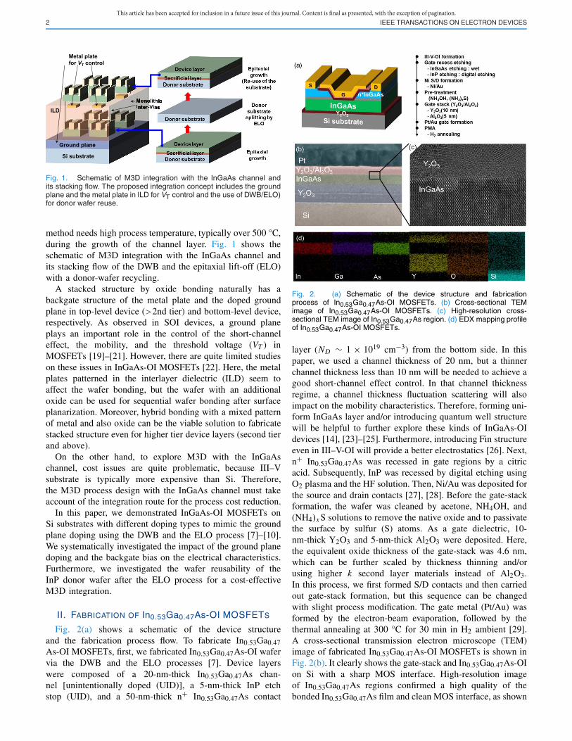
Fig. 3. (a) XRD spectra of In0.53Ga0.47As/Y2O3/Si substrates. (b) Idealand measured FWHM of XRD peak as a function of layer thickness.
in Fig. 2(c). An energy-dispersive X-ray spectroscopy (EDX)mapping image of the device in Fig. 2(d) highlights the atomicdistributions of devices, showing sharp MOS interfaces of thetop and bottom of the In0.53Ga0.47As channel.
To examine the crystal quality of bonded In0.53Ga0.47As-OI,we measured X-ray diffraction (XRD) spectra of the sam-ple. Fig. 3(a) showed the XRD spectra of transferredIn0.53Ga0.47As/InP/ In0.53Ga0.47As layer (50/5/20 nm) onSi layer. Clear two peaks were found at 63.4° and 69.2°, corre-sponding to the peaks from In0.53Ga0.47As and Si, confirmingthe high quality of In0.53Ga0.47As-OI on the Si structure. Fur-thermore, we extracted the full-width half-maximum (FWHM)of the In0.53Ga0.47As peak and plotted it in an ideal FWHMvalue calculated by Scherrer’s equation as a function of thefilm thickness in Fig. 3(b). The peak from the thin film witha thickness of 20 nm is also shown. Measured FWHM pointsclearly ride on the ideal line, showing that the DWB and theELO process allow almost perfect crystal.
III. ELECTRICAL CHARACTERISTICS OF
In0.53Ga0.47As-OI MOSFETS
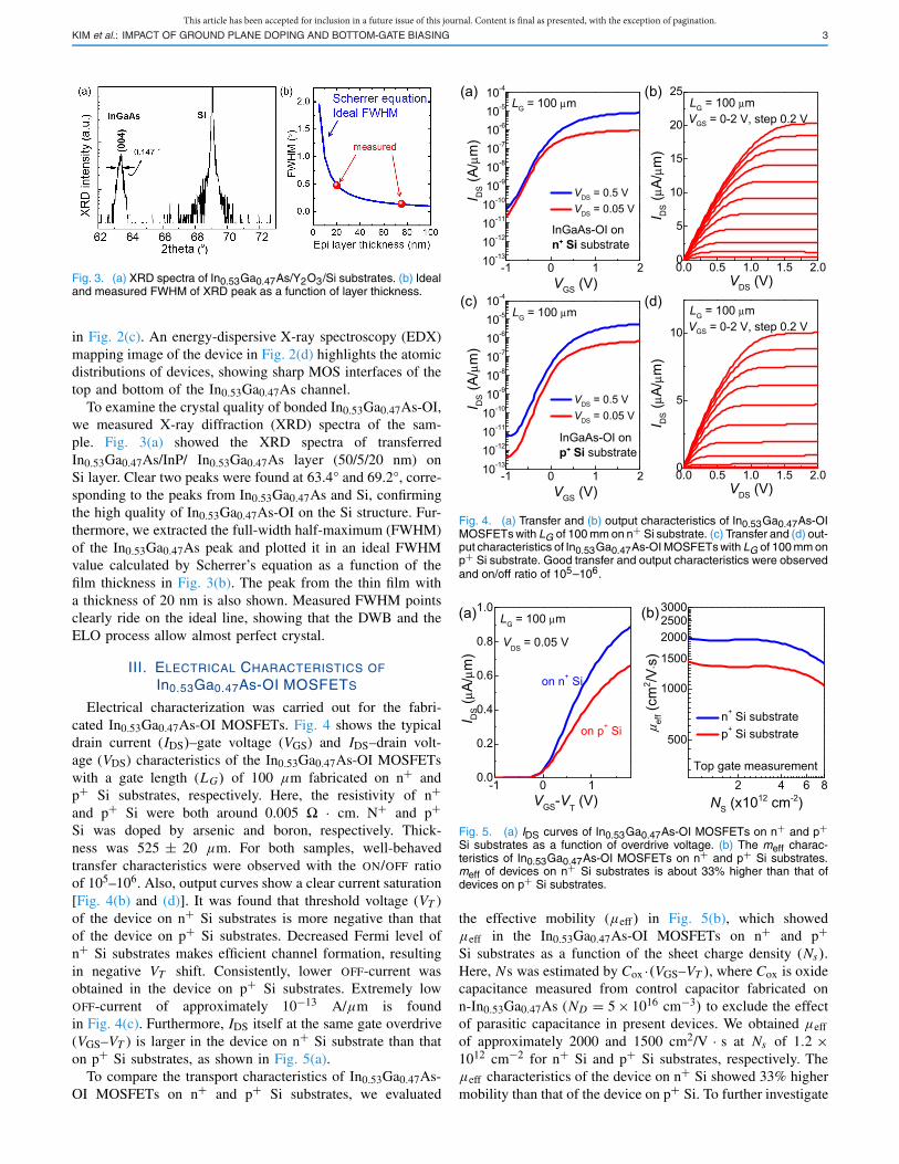
Electrical characterization was carried out for the fabri-cated In0.53Ga0.47As-OI MOSFETs. Fig. 4 shows the typicaldrain current (IDS)–gate voltage (VGS) and IDS–drain volt-age (VDS) characteristics of the In0.53Ga0.47As-OI MOSFETswith a gate length (LG) of 100 μm fabricated on n+ andp+ Si substrates, respectively. Here, the resistivity of n+and p+ Si were both around 0.005 � · cm. N+ and p+Si was doped by arsenic and boron, respectively. Thick-ness was 525 ± 20 μm. For both samples, well-behavedtransfer characteristics were observed with the ON/OFF ratioof 105–106. Also, output curves show a clear current saturation[Fig. 4(b) and (d)]. It was found that threshold voltage (VT )of the device on n+ Si substrates is more negative than thatof the device on p+ Si substrates. Decreased Fermi level ofn+ Si substrates makes efficient channel formation, resultingin negative VT shift. Consistently, lower OFF-current wasobtained in the device on p+ Si substrates. Extremely lowOFF-current of approximately 10−13 A/μm is foundin Fig. 4(c). Furthermore, IDS itself at the same gate overdrive(VGS–VT ) is larger in the device on n+ Si substrate than thaton p+ Si substrates, as shown in Fig. 5(a).
To compare the transport characteristics of In0.53Ga0.47As-OI MOSFETs on n+ and p+ Si substrates, we evaluated
Fig. 4. (a) Transfer and (b) output characteristics of In0.53Ga0.47As-OIMOSFETs with LG of 100 mm on n+ Si substrate. (c) Transfer and (d) out-put characteristics of In0.53Ga0.47As-OI MOSFETs with LG of 100 mm onp+ Si substrate. Good transfer and output characteristics were observedand on/off ratio of 105–106.
Fig. 5. (a) IDS curves of In0.53Ga0.47As-OI MOSFETs on n+ and p+Si substrates as a function of overdrive voltage. (b) The meff charac-teristics of In0.53Ga0.47As-OI MOSFETs on n+ and p+ Si substrates.meff of devices on n+ Si substrates is about 33% higher than that ofdevices on p+ Si substrates.
the effective mobility (μeff) in Fig. 5(b), which showedμeff in the In0.53Ga0.47As-OI MOSFETs on n+ and p+Si substrates as a function of the sheet charge density (Ns).Here, Ns was estimated by Cox ·(VGS–VT ), where Cox is oxidecapacitance measured from control capacitor fabricated onn-In0.53Ga0.47As (ND = 5 × 1016 cm−3) to exclude the effectof parasitic capacitance in present devices. We obtained μeffof approximately 2000 and 1500 cm2/V · s at Ns of 1.2 ×1012 cm−2 for n+ Si and p+ Si substrates, respectively. Theμeff characteristics of the device on n+ Si showed 33% highermobility than that of the device on p+ Si. To further investigate
This article has been accepted for inclusion in a future issue of this journal. Content is final as presented, with the exception of pagination.4 IEEE TRANSACTIONS ON ELECTRON DEVICES
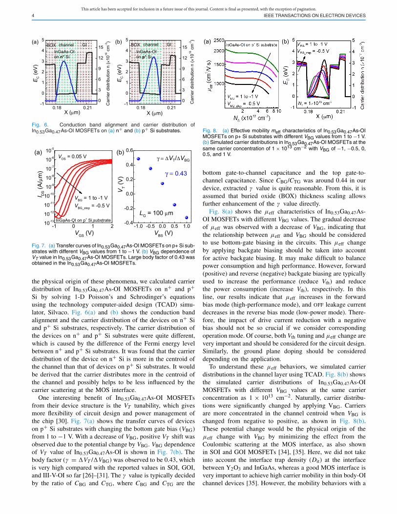
Fig. 6. Conduction band alignment and carrier distribution ofIn0.53Ga0.47As-OI MOSFETs on (a) n+ and (b) p+ Si substrates.
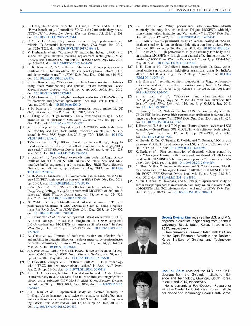
Fig. 7. (a) Transfer curves of In0.53Ga0.47As-OI MOSFETs on p+ Si sub-strates with different VBG values from 1 to −1 V. (b) VBG dependence ofVT value in In0.53Ga0.47As-OI MOSFETs. Large body factor of 0.43 wasobtained in the In0.53Ga0.47As-OI MOSFETs.
the physical origin of these phenomena, we calculated carrierdistribution of In0.53Ga0.47As-OI MOSFETs on n+ and p+Si by solving 1-D Poisson’s and Schrodinger’s equationsusing the technology computer-aided design (TCAD) simu-lator, Silvaco. Fig. 6(a) and (b) shows the conduction bandalignment and the carrier distribution of the devices on n+ Siand p+ Si substrates, respectively. The carrier distribution ofthe devices on n+ and p+ Si substrates were quite different,which is caused by the difference of the Fermi energy levelbetween n+ and p+ Si substrates. It was found that the carrierdistribution of the device on n+ Si is more in the centroid ofthe channel than that of devices on p+ Si substrates. It wouldbe derived that the carrier distributes more in the centroid ofthe channel and possibly helps to be less influenced by thecarrier scattering at the MOS interface.
One interesting benefit of In0.53Ga0.47As-OI MOSFETsfrom their device structure is the VT tunability, which givesmore flexibility of circuit design and power management ofthe chip [30]. Fig. 7(a) shows the transfer curves of deviceson p+ Si substrates with changing the bottom gate bias (VBG)from 1 to −1 V. With a decrease of VBG, positive VT shift wasobserved due to the potential change by VBG. VBG dependenceof VT value of In0.53Ga0.47As-OI is shown in Fig. 7(b). Thebody factor (γ = �VT /�VBG) was observed to be 0.43, whichis very high compared with the reported values in SOI, GOI,and III-V-OI so far [26]–[31]. The γ value is typically decidedby the ratio of CBG and CTG, where CBG and CTG are the
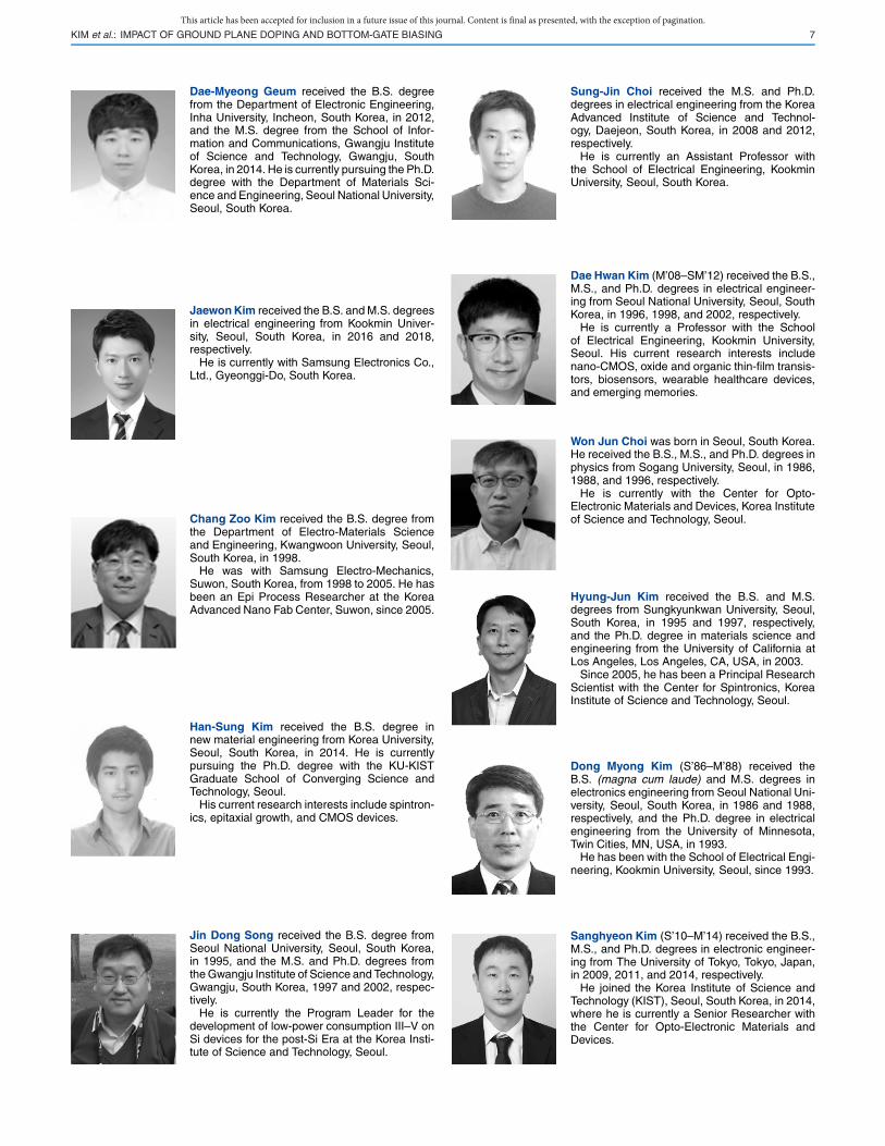
Fig. 8. (a) Effective mobility meff characteristics of In0.53Ga0.47As-OIMOSFETs on p+ Si substrates with different VBG values from 1 to −1 V.(b) Simulated carrier distributions in In0.53Ga0.47As-OI MOSFETs at thesame carrier concentration of 1 × 1013 cm−2 with VBG of −1, −0.5, 0,0.5, and 1 V.
bottom gate-to-channel capacitance and the top gate-to-channel capacitance. Since CBG/CTG was around 0.44 in ourdevice, extracted γ value is quite reasonable. From this, it isassumed that buried oxide (BOX) thickness scaling allowsfurther enhancement of the γ value directly.
Fig. 8(a) shows the μeff characteristics of In0.53Ga0.47As-OI MOSFETs with different VBG values. The gradual decreaseof μeff was observed with a decrease of VBG, indicating thatthe relationship between μeff and VBG should be consideredto use bottom-gate biasing in the circuits. This μeff changeby applying backgate biasing should be taken into accountfor active backgate biasing. It may make difficult to balancepower consumption and high performance. However, forward(positive) and reverse (negative) backgate biasing are typicallyused to increase the performance (reduce Vth) and reducethe power consumption (increase Vth), respectively. In thisline, our results indicate that μeff increases in the forwardbias mode (high-performance mode), and OFF leakage currentdecreases in the reverse bias mode (low-power mode). There-fore, the impact of drive current reduction with a negativebias should not be so crucial if we consider correspondingoperation mode. Of course, both Vth tuning and μeff change arevery important and should be considered for the circuit design.Similarly, the ground plane doping should be considereddepending on the application.
To understand these μeff behaviors, we simulated carrierdistributions in the channel layer using TCAD. Fig. 8(b) showsthe simulated carrier distributions of In0.53Ga0.47As-OIMOSFETs with different VBG values at the same carrierconcentration as 1 × 1013 cm−2. Naturally, carrier distribu-tions were significantly changed by applying VBG. Carriersare more concentrated in the channel centroid when VBG ischanged from negative to positive, as shown in Fig. 8(b).These potential change would be the physical origin of theμeff change with VBG by minimizing the effect from theCoulombic scattering at the MOS interface, as also shownin SOI and GOI MOSFETs [34], [35]. Here, we did not takeinto account the interface trap density (Dit) at the interfacebetween Y2O3 and InGaAs, whereas a good MOS interface isvery important to achieve high carrier mobility in thin body-OIchannel devices [35]. However, the mobility behaviors with a

This article has been accepted for inclusion in a future issue of this journal. Content is final as presented, with the exception of pagination.KIM et al.: IMPACT OF GROUND PLANE DOPING AND BOTTOM-GATE BIASING 5
Fig. 9. AFM images of the In0.53Ga0.47As surface grown on (a) freshand regrown In0.53Ga0.47As surface on reused InP substrates with(b) H3PO4- and (c) citric acid-based treatments before the epitaxialgrowth. (d) Raman spectra of the In0.53Ga0.47As surface of the samesample for AFM measurement.
different backgate biasing can still be explained by the relativecarrier distribution across the channel layer, because the back-MOS interface and front MOS interface are the same as that ofY2O3/InGaAs and should have similar interfacial properties.
Considering physical dimension of the devices, thinnerY2O3 BOX will provide more sensitive change of the potentialdistribution, which leads to the change of μeff , as thinnerBOX provides a larger body factor (γ ∝ CBG/CTG).
Also, to address the cost issue of the III–V layer stack-ing, we investigated the wafer reusability of the InP donorwafer by treating the surface after ELO process. After grow-ing the In0.53Ga0.47As/AlAs layer on InP, we mimicked theELO process and removed all of the layers on InP withtwo different treatments of H3PO4-based and citric acid-basedsolutions. Sequentially, we repeated the epitaxial growth ofthe In0.53Ga0.47As layers and the fabrication of MOSFETs onthese treated wafers.
The quality of the epitaxial layers on the fresh andreused InP substrates was comparatively evaluated through theAFM image and the Raman spectra. Fig. 9(a)–(c) shows theAFM images of the fresh and reused wafers with two differenttreatments before the growth. They showed very smoothsurface with Rrms of 0.16, 0.17, and 0.17 nm, indicating thata smooth epitaxial layer surface can be obtained even onthe reused InP wafer. Fig. 9(d) shows the Raman shift ofthe reused wafer from the fresh wafer. The Raman shift ofthe In0.53Ga0.47As layer grown on the reused wafers withboth pretreatments before the epitaxial growth was comparableto that from the In0.53Ga0.47As layer grown on the freshInP wafer.
Finally, to investigate the electrical properties of the epi-taxial layer grown on reused wafer, we fabricated typicalIn0.53Ga0.47As on InP MOSFETs [28]. Fig. 10 showed transferand mobility characteristics of devices from fresh and reusedwafer, respectively. Transfer and mobility characteristics ofdevice from reused wafer with H3PO4-based solution treat-ment showed almost comparable characteristics with that ofthe device from fresh wafer. These results indicate that waferseparated from the device layer during the ELO can be reusedfor a next epitaxial growth, which lead to dramatic costreduction for the device layer stacking toward M3D integration
Fig. 10. (a) Transfer curves and (b) comparative effective mobilityµeff characteristics of the In0.53Ga0.47As grown on fresh and reusedInP substrates.
with In0.53Ga0.47As channel materials. However, that citricacid-based solution-treated sample shows slightly a smallermobility than H3PO4-based solution-treated sample and thecontrol sample on a fresh substrate, whereas surface mor-phology was almost the same. These results strongly indicatethat surface roughness is not only impacting a factor for theepitaxial growth, and chemical termination or surface prepa-ration before the growth is also an important factor for thereusability of the wafer after chemical treatment. We believethat dedicated surface preparation before the growth should befurther explored, since this will also impact on the variabilityand reliability in short-channel devices.
IV. CONCLUSION
In this paper, we fabricated In0.53Ga0.47As-OI MOSFETs onn+ and p+ Si substrates using the DWB and the ELO processesand systematically investigated the effect of the ground planedoping (n+ and p+ Si) and the backgate biasing on electricalproperties of devices. The ground plane doping, represented bythe doping of the bottom Si substrate, and the backgate biasinggreatly influence on VT and effective mobility characteristicsof devices as shown before. Furthermore, for cost reductionof In0.53Ga0.47As stacking processes, we investigated thereusability of InP substrates for the sequential epitaxial growth.We obtained very smooth and sharp Raman spectra of theIn0.53Ga0.47As layer grown on a reused wafer. FabricatedIn0.53Ga0.47As MOSFETs grown on a reused InP wafer alsoshowed almost identical transfer and mobility characteristicswith those from the fresh InP wafer. We expect that theproposed scheme provides a possible tuning of mobility andVT and cost-effective In0.53Ga0.47As-OI fabrication for M3Dintegration.
REFERENCES
[1] S. K. Samal, D. Nayak, M. Ichihashi, S. Banna, and S. K. Lim, “Mono-lithic 3D IC vs. TSV-based 3D IC in 14 nm FinFET technology,” in Proc.IEEE S3S Conf., Oct. 2016, pp. 1–2, doi: 10.1109/S3S.2016.7804405.
[2] M. Vinet et al., “Monolithic 3D integration: A powerful alternative toclassical 2D scaling,” in Proc. IEEE S3S Conf., Oct. 2014, pp. 1–3,doi: 10.1109/S3S.2014.7028194.
[3] C.-C. Yang et al., “Footprint-efficient and power-saving monolithic IoT3D+ IC constructed by BEOL-compatible sub-10nm high aspect ratio(AR>7) single-grained Si FinFETs with record high Ion of 0.38 mA/μmand steep-swing of 65 mV/dec. and Ion/Ioff ratio of 8,” in IEDM Tech.Dig., Dec. 2016, pp. 224–227, doi: 10.1109/IEDM.2016.7838379.
This article has been accepted for inclusion in a future issue of this journal. Content is final as presented, with the exception of pagination.6 IEEE TRANSACTIONS ON ELECTRON DEVICES
[4] K. Chang, K. Acharya, S. Sinha, B. Cline, G. Yeric, and S. K. Lim,“Power benefit study of monolithic 3D IC at the 7 nm technology node,”IEEE/ACM Int. Symp. Low Power Electron. Design, Jul. 2015, p. 201,doi: 10.1109/ISLPED.2015.7273514.
[5] C.-M. V. Lu et al., “Key process steps for high performance andreliable 3D Sequential Integration,” in Proc. VLSI Symp., Jun. 2017,pp. T226–T227, doi: 10.23919/VLSIT.2017.7998181.
[6] V. Deshpande et al., “Advanced 3D monolithic hybrid CMOS withsub-50 nm gate inverters featuring replacement metal gate (RMG)-InGaAs nFETs on SiGe-OI Fin pFETs,” in IEDM Tech. Dig., Dec. 2015,pp. 209–212, doi: 10.1109/IEDM.2015.7409658.
[7] S. K. Kim et al., “Cost-effective fabrication of In0.53Ga0.47As-on-insulator on Si for monolithic 3D via novel epitaxial lift-off (ELO)and donor wafer re-use,” in IEDM Tech. Dig., Dec. 2016, pp. 616–619,doi: 10.1109/IEDM.2016.7838479.
[8] S. K. Kim et al., “Fabrication of InGaAs-on-insulator substratesusing direct wafer-bonding and epitaxial lift-off techniques,” IEEETrans. Electron Devices, vol. 64, no. 9, pp. 3601–3608, Sep. 2017,doi: 10.1109/TED.2017.2722482.
[9] D.-M. Geum et al., “Ultra-high-throughput production of III–V/Si waferfor electronic and photonic applications,” Sci. Rep., vol. 6, Feb. 2016,Art. no. 20610, doi: 10.1038/srep20610.
[10] S.-H. Kim et al., “Heterogeneous integration toward monolithic 3Dchip,” in Proc. IEEE S3S Conf., Oct. 2017, paper 7.2.
[11] S. Takagi et al., “High mobility CMOS technologies using III–V/Gechannels on Si platform,” Solid-State Electron., vol. 88, pp. 2–8,Oct. 2013, doi: 10.1016/j.sse.2013.04.020.
[12] M. L. Huang et al., “In0.53Ga0.47As MOSFETs with high chan-nel mobility and gate stack quality fabricated on 300 mm Si sub-strate,” in Proc. VLSI Symp., Jun. 2015, pp. T204–T205, doi: 10.1109/VLSIT.2015.7223675.
[13] T.-W. Kim et al., “Lg=80 -nm trigate quantum-well In0.53Ga0.47Asmetal–oxide–semiconductor field-effect transistors with Al2O3/HfO2gate-stack,” IEEE Electron Device Lett., vol. 36, no. 3, pp. 223–225,Mar. 2015, doi: 10.1109/LED.2015.2393554.
[14] S. Kim et al., “Sub-60-nm extremely thin body Inx Ga1−x As-on-insulator MOSFETs on Si with Ni-InGaAs metal S/D and MOSinterface buffer engineering and its scalability,” IEEE Trans. ElectronDevices, vol. 60, no. 8, pp. 2512–2517, Aug. 2013, doi: 10.1109/TED.2013.2270558.
[15] C. B. Zota, F. Lindelow, L.-E. Wernersson, and E. Lind, “InGaAs tri-gate MOSFETs with record on-current,” in IEDM Tech. Dig., Dec. 2016,pp. 55–58, doi: 10.1109/IEDM.2016.7838336.
[16] S.-W. Son et al., “Record effective mobility obtained fromIn0.53Ga0.47As/In0.52Al0.48As quantum-well MOSFETs on 300-mm Sisubstrate,” IEEE Electron Device Lett., vol. 38, no. 6, pp. 724–727,Jun. 2017, doi: 10.1109/LED.2017.2695652.
[17] N. Waldron et al., “Gate-all-around InGaAs nanowire FETS withpeak transconductance of 2200 μS/μm at 50nm Lg using a replace-ment Fin RMG flow,” in IEDM Tech. Dig., Dec. 2015, pp. 799–802,doi: 10.1109/IEDM.2015. 7409805.
[18] L. Czornomaz et al., “Confined epitaxial lateral overgrowth (CELO):A novel concept for scalable integration of CMOS-compatibleInGaAs-on-insulator MOSFETs on large-area Si substrates,” in Proc.VLSI Symp., Jun. 2015, pp. T172–T173, doi: 10.1109/VLSIT.2015.7223666.
[19] A. Ohata et al., “Impact of back-gate biasing on effective fieldand mobility in ultrathin silicon-on-insulator metal-oxide-semiconductorfield-effect-transistors,” J. Appl. Phys., vol. 113, no. 14, p. 144514,Mar. 2013, doi: 10.1063/1.4799612.
[20] J.-P. Noel et al., “Multi-VT UTBB FDSOI device architectures for low-power CMOS circuit,” IEEE Trans. Electron Devices, vol. 58, no. 8,pp. 2473–2482, May 2010, doi: 10.1109/TED.2011.2155658.
[21] C. Fenouillet-Beranger et al., “Efficient multi-VT FDSOI technologywith UTBOX for low power circuit design,” in Proc. VLSI Symp.,Jun. 2010, pp. 65–66, doi: 10.1109/VLSIT.2010. 5556118.
[22] J. Lin, L. Czornomaz, N. Daix, D. A. Antoniadis, and J. A. del Alamo,“Ultrathin body InGaAs MOSFETs on III–V-on-insulator integrated withsilicon active substrate (III-V-OIAS),” IEEE Trans. Electron Devices,vol. 63, no. 89, pp. 3088–3095, Aug. 2016, doi: 10.1109/TED.2016.2579642.
[23] S.-H. Kim et al., “Experimental study on electron mobility inInx Ga1−x As-on-insulator metal-oxide-semiconductor field-effect tran-sistors with in content modulation and MOS interface buffer engineer-ing,” IEEE Trans. Nanotechnol., vol. 12, no. 4, pp. 621–628, Jul. 2013,doi: 10.1109/TNANO.2013.2265435.
[24] S.-H. Kim et al., “High performance sub-20-nm-channel-lengthextremely-thin body InAs-on-insulator Tri-gate MOSFETs with highshort channel effect immunity and Vth tunability,” in IEDM Tech. Dig.,Dec. 2013, pp. 429–432, doi: 10.1109/IEDM.2013.6724642.
[25] S.-H. Kim et al., “Experimental study on vertical scaling of InAs-on-insulator metal-oxide-semiconductor field-effect transistors,” Appl. Phys.Lett., vol. 104, no. 26, p. 263507, Jun. 2014, doi: 10.1063/1.4885765.
[26] S.-H. Kim et al., “High performance tri-gate extremely thin-body InAs-on-insulator MOSFETs with high short channel effect immunity and Vthtunability,” IEEE Trans. Electron Devices, vol. 61, no. 5, pp. 1354–1360,May 2014, doi: 10.1109/TED.2014.2312546.
[27] S. H. Kim et al., “Self-aligned metal source/drain Inx Ga1−x As n-metal–oxide–semiconductor field-effect transistors using Ni–InGaAsalloy,” in IEDM Tech. Dig., Dec. 2010, pp. 596–599, doi: 10.1109/IEDM.2010.5703429.
[28] S. H. Kim et al., “Self-aligned metal source/drain Inx Ga1−x As n-metal–oxide–semiconductor field-effect transistors using Ni–InGaAs alloy,”Appl. Phy. Exp., vol. 4, no. 2, pp. 024201-1–024201-3, Jan. 2011, doi:10.1143/APEX.4.024201.
[29] S. K. Kim et al., “Fabrication and characterization ofPt/Al2O3/Y2O3/In0.53Ga0.47As MOSFETs with low interface trapdensity,” Appl. Phys. Lett., vol. 110, no. 4, p. 043501, Jan. 2017,doi: 10.1063/1.4974893.
[30] R. Tsuchiya et al., “Silicon on thin BOX: A new paradigm of theCMOSFET for low-power high-performance application featuring wide-range back-bias control,” in IEDM Tech. Dig., Dec. 2004, pp. 631–634,doi: 10.1109/IEDM.2004.1419245.
[31] T. Hiramoto, T. Saito, and T. Nagumo, “Future electron devices and SOItechnology—Semi-Planar SOI MOSFETs with sufficient body effect,”Jpn. J. Appl. Phys., vol. 42, no. 4B, pp. 1975–1978, Apr. 2003,doi: 10.1143/JJAP.42.1975.
[32] M. Saitoh, K. Ota, C. Tanaka, K. Uchida, and T. Numata, “SOI tri-gatenanowire MOSFETs for ultra-low power LSI,” in Proc. IEEE SOI Conf.,Oct. 2012, pp. 1–2, doi: 10.1109/SOI.2012.6404396.
[33] K. Ikeda et al., “First demonstration of threshold voltage control bysub-1V back-gate biasing for thin body and buried-oxide (TBB) Ge-on-insulator (GOI) MOSFETs for low-power operation,” in Proc. IEEE SOIConf., Oct. 2012, pp. 1–2, doi: 10.1109/SOI.2012.6404354.
[34] A. Ohata, Y. Bae, C. Fenouillet-Beranger, and S. Cristoloveanu, “Mobil-ity enhancement by back-gate biasing in ultrathin SOI MOSFETs withthin BOX,” IEEE Electron Device Lett., vol. 33, no. 3, pp. 348–350,Mar. 2012, doi: 10.1109/LED.2011.2181816.
[35] X. Yu, J. Kang, M. Takenaka, and S. Takagi, “Experimental study oncarrier transport properties in extremely-thin body Ge-on-insulator (GOI)p-MOSFETs with GOI thickness down to 2 nm,” in IEDM Tech. Dig.,Dec. 2015, pp. 20–23, doi: 10.1109/IEDM.2015.7409611.
Seong Kwang Kim received the B.S. and M.S.degrees in electrical engineering from KookminUniversity, Seoul, South Korea, in 2015 and2017, respectively.
He is currently a Research Intern with the Cen-ter for Opto-Electronic Materials and Devices,Korea Institute of Science and Technology,Seoul.
Jae-Phil Shim received the M.S. and Ph.D.degrees from the Gwangju Institute of Sci-ence and Technology, Gwangju, South Korea,in 2011 and 2015, respectively.
He is currently a Post-Doctoral Researcherwith the Center for Spintronics, Korea Instituteof Science and Technology, Seoul, South Korea.
This article has been accepted for inclusion in a future issue of this journal. Content is final as presented, with the exception of pagination.KIM et al.: IMPACT OF GROUND PLANE DOPING AND BOTTOM-GATE BIASING 7
Dae-Myeong Geum received the B.S. degreefrom the Department of Electronic Engineering,Inha University, Incheon, South Korea, in 2012,and the M.S. degree from the School of Infor-mation and Communications, Gwangju Instituteof Science and Technology, Gwangju, SouthKorea, in 2014. He is currently pursuing the Ph.D.degree with the Department of Materials Sci-ence and Engineering, Seoul National University,Seoul, South Korea.
Jaewon Kim received the B.S. and M.S. degreesin electrical engineering from Kookmin Univer-sity, Seoul, South Korea, in 2016 and 2018,respectively.
He is currently with Samsung Electronics Co.,Ltd., Gyeonggi-Do, South Korea.
Chang Zoo Kim received the B.S. degree fromthe Department of Electro-Materials Scienceand Engineering, Kwangwoon University, Seoul,South Korea, in 1998.
He was with Samsung Electro-Mechanics,Suwon, South Korea, from 1998 to 2005. He hasbeen an Epi Process Researcher at the KoreaAdvanced Nano Fab Center, Suwon, since 2005.
Han-Sung Kim received the B.S. degree innew material engineering from Korea University,Seoul, South Korea, in 2014. He is currentlypursuing the Ph.D. degree with the KU-KISTGraduate School of Converging Science andTechnology, Seoul.
His current research interests include spintron-ics, epitaxial growth, and CMOS devices.
Jin Dong Song received the B.S. degree fromSeoul National University, Seoul, South Korea,in 1995, and the M.S. and Ph.D. degrees fromthe Gwangju Institute of Science and Technology,Gwangju, South Korea, 1997 and 2002, respec-tively.
He is currently the Program Leader for thedevelopment of low-power consumption III–V onSi devices for the post-Si Era at the Korea Insti-tute of Science and Technology, Seoul.
Sung-Jin Choi received the M.S. and Ph.D.degrees in electrical engineering from the KoreaAdvanced Institute of Science and Technol-ogy, Daejeon, South Korea, in 2008 and 2012,respectively.
He is currently an Assistant Professor withthe School of Electrical Engineering, KookminUniversity, Seoul, South Korea.
Dae Hwan Kim (M’08–SM’12) received the B.S.,M.S., and Ph.D. degrees in electrical engineer-ing from Seoul National University, Seoul, SouthKorea, in 1996, 1998, and 2002, respectively.
He is currently a Professor with the Schoolof Electrical Engineering, Kookmin University,Seoul. His current research interests includenano-CMOS, oxide and organic thin-film transis-tors, biosensors, wearable healthcare devices,and emerging memories.
Won Jun Choi was born in Seoul, South Korea.He received the B.S., M.S., and Ph.D. degrees inphysics from Sogang University, Seoul, in 1986,1988, and 1996, respectively.
He is currently with the Center for Opto-Electronic Materials and Devices, Korea Instituteof Science and Technology, Seoul.
Hyung-Jun Kim received the B.S. and M.S.degrees from Sungkyunkwan University, Seoul,South Korea, in 1995 and 1997, respectively,and the Ph.D. degree in materials science andengineering from the University of California atLos Angeles, Los Angeles, CA, USA, in 2003.
Since 2005, he has been a Principal ResearchScientist with the Center for Spintronics, KoreaInstitute of Science and Technology, Seoul.
Dong Myong Kim (S’86–M’88) received theB.S. (magna cum laude) and M.S. degrees inelectronics engineering from Seoul National Uni-versity, Seoul, South Korea, in 1986 and 1988,respectively, and the Ph.D. degree in electricalengineering from the University of Minnesota,Twin Cities, MN, USA, in 1993.
He has been with the School of Electrical Engi-neering, Kookmin University, Seoul, since 1993.
Sanghyeon Kim (S’10–M’14) received the B.S.,M.S., and Ph.D. degrees in electronic engineer-ing from The University of Tokyo, Tokyo, Japan,in 2009, 2011, and 2014, respectively.
He joined the Korea Institute of Science andTechnology (KIST), Seoul, South Korea, in 2014,where he is currently a Senior Researcher withthe Center for Opto-Electronic Materials andDevices.


![S!LKsilk.kookmin.ac.kr/img_up/shop_pds/kmusilk/contents/my... · 2013-07-15 · 5 ijI (äNM 6 K3 q l ¤ Å=R X. Y [ " u4 " v+-X. wx. a\ #4 6]WX. wx. yX. Y. Zz ýé](https://img.pdfslide.net/doc/110x75/5f1645e87526bf13c9727c7a/s-2013-07-15-5-iji-nm-6-k3-q-l-r-x-y-u4-v-x-wx-a.jpg)