Embed Size (px)
Citation preview
IEEE TRANSACTIONS ON ELECTRONICS PACKAGING MANUFACTURING, VOL. 30, NO. 2, APRIL 2007 115
Surface Resistivity Characterization of NewPrinted Circuit Board Materials for Use
in Spacecraft ElectronicsAndrea Bulletti, Lorenzo Capineri, Senior Member, IEEE, Maurizio Materassi, and Barrie D. Dunn
Abstract—New dielectric materials have been introduced forprinted circuit board applications, such as Thermount and poly-imide with the aim to match the requirements for high speed andhigh density of electronic devices that are planned for new space-craft electronic boards. Before these newer substrate can fullyreplace the well-known space-approved material epoxy FR-4, it isnecessary to investigate more deeply their electrical and mechan-ical properties. The scope of this study is to report quantitativecharacterization of the surface resistivity for the different materialsamples under various testing conditions that include relativehumidity, temperature, solder flux contamination, and coronadischarge. The surface resistivity results are reported for sets ofsamples measured under a combination of testing conditions.
Index Terms—Corona discharge, electrical insulation testing,flux contamination, printed circuit boards (PCBs), surface resis-tivity.
I. INTRODUCTION
THE DESIGN of electronic printed circuit boards (PCBs),with high-density/high-speed components, requires the
design and fabrication of multilayered printed circuits on di-electric substrates with high-quality materials. Over the years,electronic components manufacturers have decreased packagepin pitch from 1.27 mm less than 0.5 mm. It is also necessaryto find materials for PCBs with a high glass temperature ( )and low thermal expansion coefficient (CTE) in order to usehigh-temperature soldering processes and multilayered PCBs.Meanwhile the operating frequency of digital and telecom-munications electronic components are rapidly reaching the1-GHz frequency. This trend will also be followed by spacetechnology, and there is a need to develop electronic packagingapplications which are lighter, faster, and smaller. There arenow commercially available high-quality materials like Ther-mount and polyimide that are good candidates to replace thewell-known glass epoxy composite laminate, FR-4, that hasbeen the workhorse for European PCB assemblers. Thermount
Manuscript received December 14, 2005; revised September 28, 2006.A. Bulletti and L. Capineri are with the Department of Electronics and
Telecommunications, University of Florence, 50139 Florence, Italy (e-mail:[email protected]).
M. Materassi is with the Alcatel Alenia Space Italia, 50013 Campi Bisenzio(Florence), Italy.
B. D. Dunn is with the Materials and Processes Division, ESA-Estec, 2200AGNoordwijk, The Netherlands.
Color versions of one or more of the figures in this paper are available onlineat http://ieeexplore.ieee.org.
Digital Object Identifier 10.1109/TEPM.2007.899075
is a laminate of epoxy and nonwoven aramid (100%) rein-forcement manufactured by Dupont. Thermount offers severalperformance benefits over standard materials: low in-plane CTE(7–9 ppm C) depending on resin content; high (240 C);low dielectric constant (4.0); provides excellent dimensionalstability ( 0.03 ); improves fine feature formation due toits smooth surface; and enables high-speed laser microviaformation [1]. However, Thermount absorbs more moisturein respect to standard glass epoxy materials when exposedto high-humidity and high-temperature conditions [2], andmoisture level in a dielectric substrate could significantly af-fect the electrical properties. Also, polyimide material offersseveral performance benefits Thermount material: low -axisCTE (45 ppm C); high ( 250 C), but it absorbs moremoisture with respect to standard glass epoxy materials whenexposed to high-humidity and high temperature conditions.
Electrical characteristics of these materials are often guaran-teed in standard operating conditions, but the influence of thecombined action of several environmental factors is not yet fullyinvestigated. According to a previous work [3], the surface in-sulation resistance (SIR) test has been adopted in the present in-vestigation to show the different behavior of dielectric substratesfor PCBs, and results are reported for SIR measurements car-ried out according to IPC-TM-650 [4]. The influence of thermalexcursion, voltage bias, and solder flux influence was also ad-dressed as being relevant for the electromigration process thatlead to the formation of conductive anodic filaments underneathcopper pads or between vias.
The aim of this paper is to experimentally characterize thesurface resistivity ( ) of base laminates (i.e., epoxy, Ther-mount, and polyimide) when subjected of the following con-ditioning factors relevant for use of electronic boards in spaceenvironment:
• relative humidity (RH);• temperature;• solder flux contaminations;• corona discharge (CD) and outgassing phenomena in
vacuum (at 10 mbar).Preliminary data related to surface and volume resistivity valueswere searched in the technical notes and data sheets availablefrom the laminate manufacturers of epoxy, polyimide, and Ther-mount materials. These values were difficult to compare becauseeach referred to different test conditions of the materials: tem-perature, relative humidity, testing time (duration). For example,some values were referred to test condition C-96/35/90 (that
1521-334X/$25.00 © 2007 IEEE
116 IEEE TRANSACTIONS ON ELECTRONICS PACKAGING MANUFACTURING, VOL. 30, NO. 2, APRIL 2007
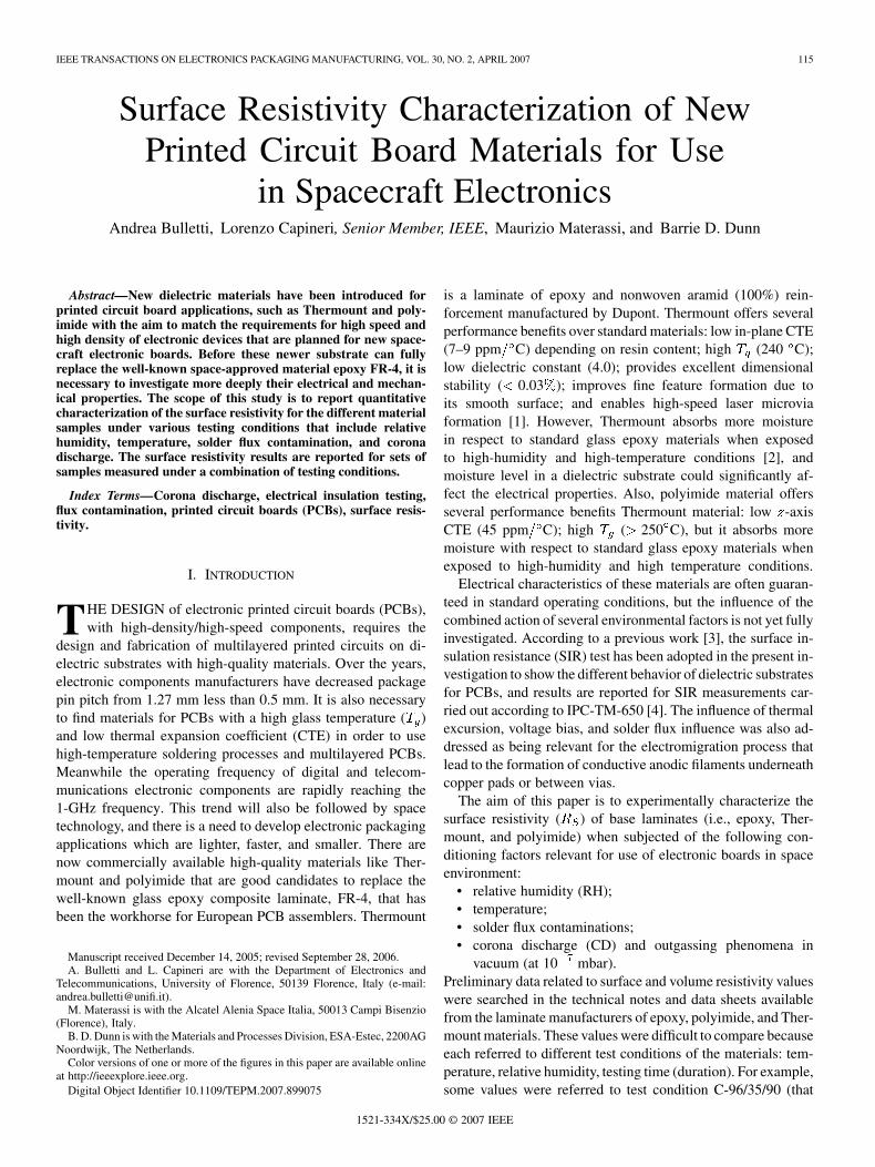
Fig. 1. Experimental setup for humidity and temperature conditioning tests (; =300 mm, h =400 mm, ; =180 mm, h =300 mm).
means a treatment for 96 h at 35 C and at 90% RH) or testcondition E-24/125 (that means a treatment for 24 h at 125 C)[5].
Previous work [6], [7] report test results on the humidity/tem-perature conditioning of epoxy PCBs for 48 h; it was demon-strated that humidity absorption by this material caused a varia-tion of surface resistivity and that the water absorption changedwith an increase in temperature. The effect of water (high hu-midity) on these various laminates is extremely important forhigh-reliability circuits. In the space industry, the cleaning offlux residues is achieved by using alcohol mixed with water, toremove organic and ionic contaminants, respectively. Absorp-tion of water into the laminate occurs during each soldering andcomponent rework or repair operation and post-baking of theassembly does not always remove all moisture [8]. This mois-ture absorption (measured after baking samples when there is amass loss) of epoxy and polyimide materials were described in arecent ESA study performed by the Insitut de Soudure (France)[8].
Moreover, from the data obtained in the literature, it is diffi-cult to compare the influence of different testing environmentsbecause the samples preparation and measurement setup for sur-face resistivity are not fully described by the authors.
For our experimentation, we decided to perform measure-ments on 120 samples per substrate material. Such a largenumber of samples have not been utilized before, and it isexpected to provide a statistically significant results.
The analysis of variation in surface resistivity after differenttest procedures is reported in the conclusions and a correlationwith physical properties of tested materials is attempted.
II. TEST PROCEDURES
In general, surface resistivity of dielectric composites isinfluenced by several environmental factors, so it was necessaryto establish the sequence of treatments for the batch ofsamples.
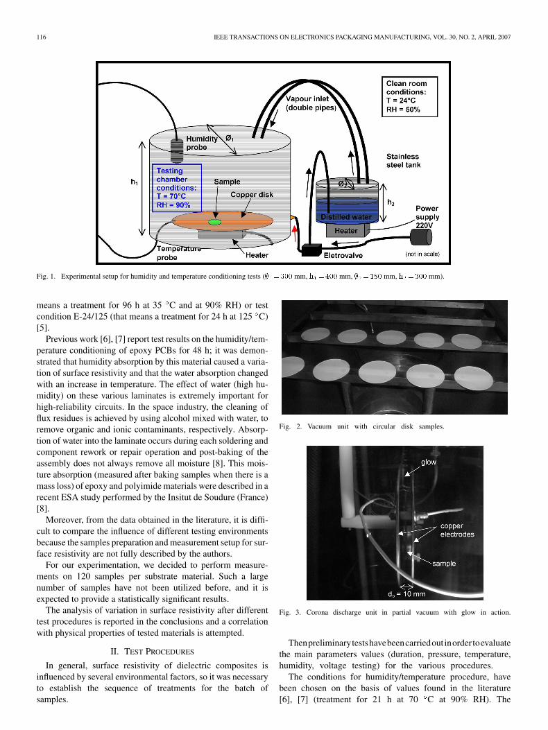
Fig. 2. Vacuum unit with circular disk samples.
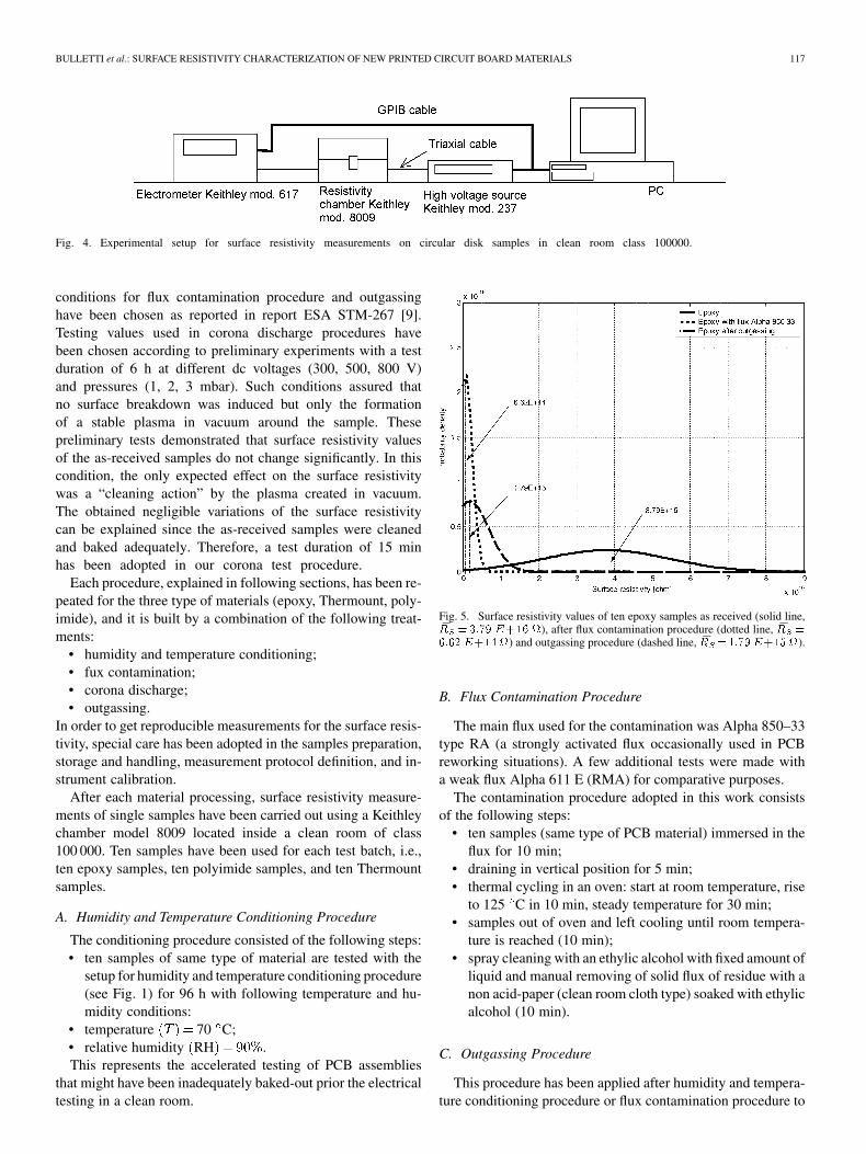
Fig. 3. Corona discharge unit in partial vacuum with glow in action.
Thenpreliminarytestshavebeencarriedoutinordertoevaluatethe main parameters values (duration, pressure, temperature,humidity, voltage testing) for the various procedures.
The conditions for humidity/temperature procedure, havebeen chosen on the basis of values found in the literature[6], [7] (treatment for 21 h at 70 C at 90% RH). The
BULLETTI et al.: SURFACE RESISTIVITY CHARACTERIZATION OF NEW PRINTED CIRCUIT BOARD MATERIALS 117
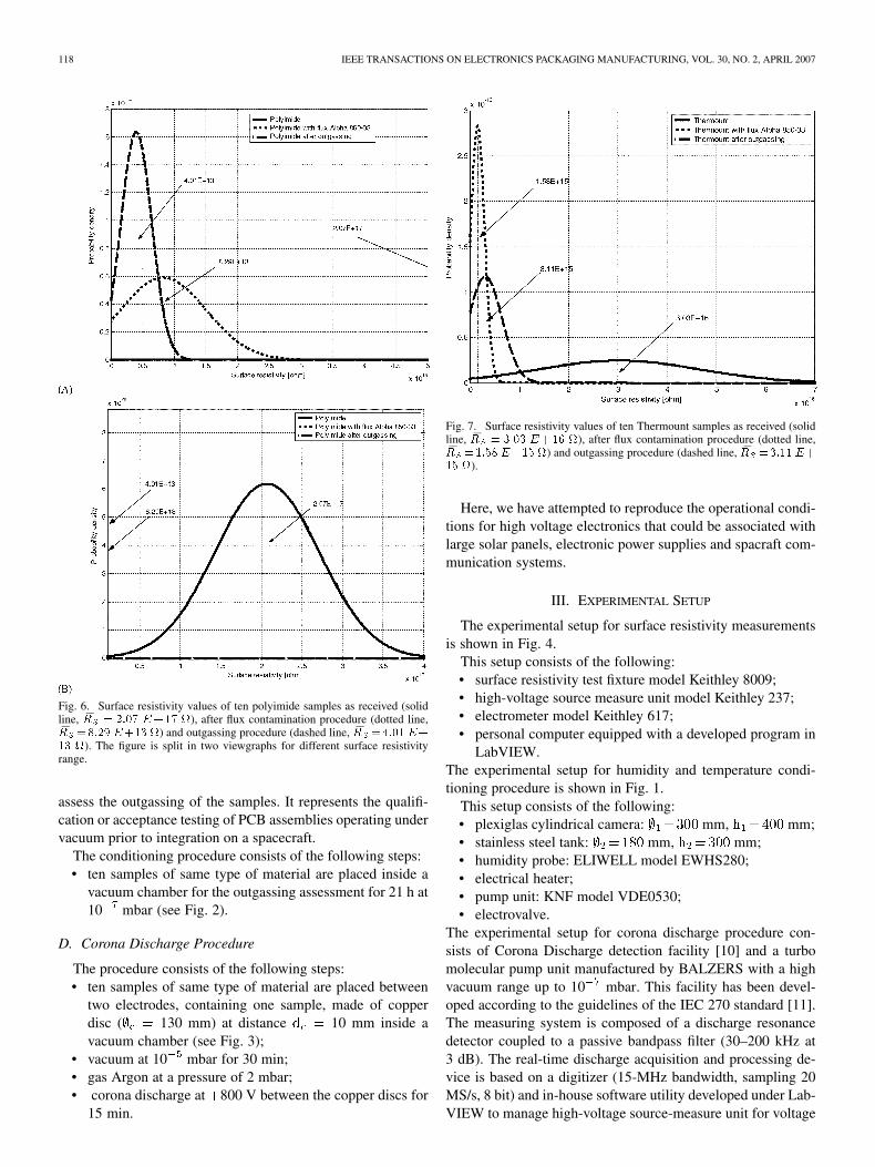
Fig. 4. Experimental setup for surface resistivity measurements on circular disk samples in clean room class 100000.
conditions for flux contamination procedure and outgassinghave been chosen as reported in report ESA STM-267 [9].Testing values used in corona discharge procedures havebeen chosen according to preliminary experiments with a testduration of 6 h at different dc voltages (300, 500, 800 V)and pressures (1, 2, 3 mbar). Such conditions assured thatno surface breakdown was induced but only the formationof a stable plasma in vacuum around the sample. Thesepreliminary tests demonstrated that surface resistivity valuesof the as-received samples do not change significantly. In thiscondition, the only expected effect on the surface resistivitywas a “cleaning action” by the plasma created in vacuum.The obtained negligible variations of the surface resistivitycan be explained since the as-received samples were cleanedand baked adequately. Therefore, a test duration of 15 minhas been adopted in our corona test procedure.
Each procedure, explained in following sections, has been re-peated for the three type of materials (epoxy, Thermount, poly-imide), and it is built by a combination of the following treat-ments:
• humidity and temperature conditioning;• fux contamination;• corona discharge;• outgassing.
In order to get reproducible measurements for the surface resis-tivity, special care has been adopted in the samples preparation,storage and handling, measurement protocol definition, and in-strument calibration.
After each material processing, surface resistivity measure-ments of single samples have been carried out using a Keithleychamber model 8009 located inside a clean room of class100 000. Ten samples have been used for each test batch, i.e.,ten epoxy samples, ten polyimide samples, and ten Thermountsamples.
A. Humidity and Temperature Conditioning Procedure
The conditioning procedure consisted of the following steps:• ten samples of same type of material are tested with the
setup for humidity and temperature conditioning procedure(see Fig. 1) for 96 h with following temperature and hu-midity conditions:
• temperature 70 C;• relative humidity RH .This represents the accelerated testing of PCB assemblies
that might have been inadequately baked-out prior the electricaltesting in a clean room.
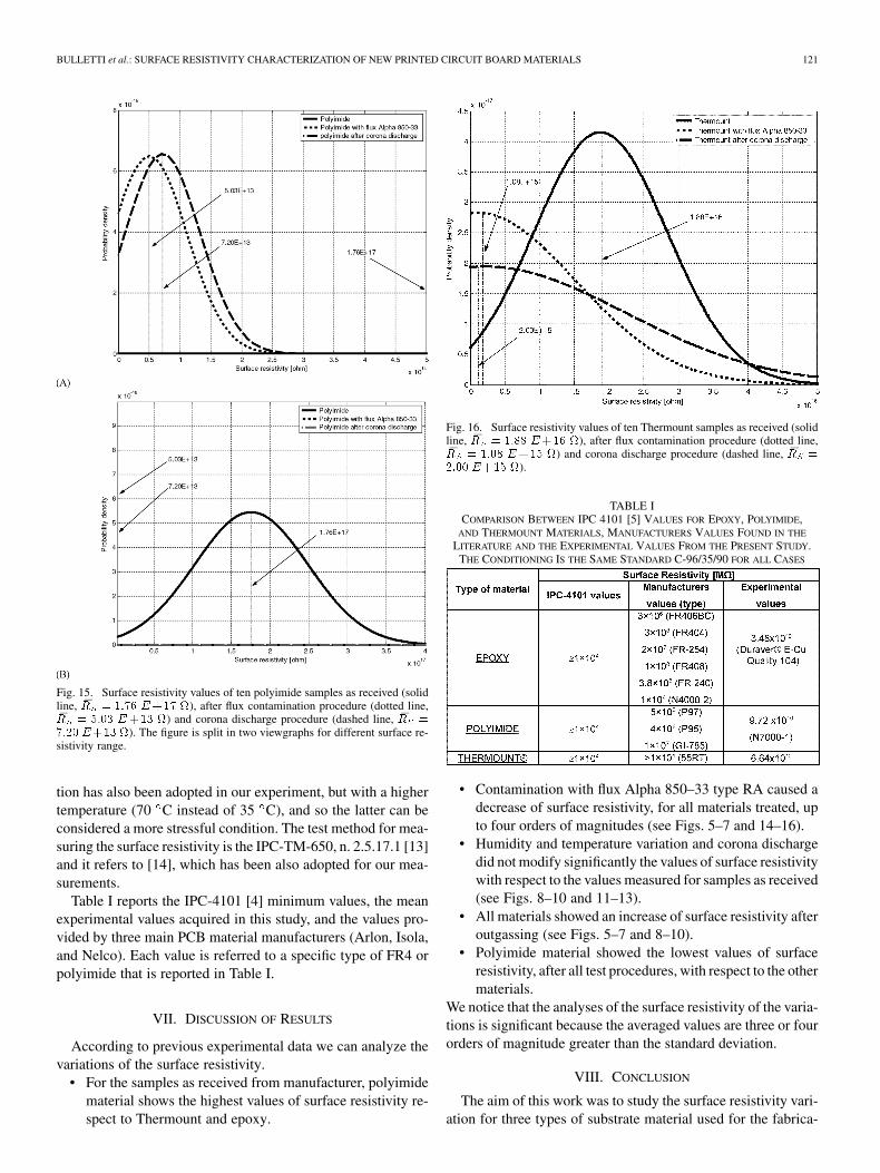
Fig. 5. Surface resistivity values of ten epoxy samples as received (solid line,�R =3:79 E+16 ), after flux contamination procedure (dotted line, �R =
6:62 E+14 ) and outgassing procedure (dashed line, �R =1:79E+15 ).
B. Flux Contamination Procedure
The main flux used for the contamination was Alpha 850–33type RA (a strongly activated flux occasionally used in PCBreworking situations). A few additional tests were made witha weak flux Alpha 611 E (RMA) for comparative purposes.
The contamination procedure adopted in this work consistsof the following steps:
• ten samples (same type of PCB material) immersed in theflux for 10 min;
• draining in vertical position for 5 min;• thermal cycling in an oven: start at room temperature, rise
to 125 C in 10 min, steady temperature for 30 min;• samples out of oven and left cooling until room tempera-
ture is reached (10 min);• spray cleaning with an ethylic alcohol with fixed amount of
liquid and manual removing of solid flux of residue with anon acid-paper (clean room cloth type) soaked with ethylicalcohol (10 min).
C. Outgassing Procedure
This procedure has been applied after humidity and tempera-ture conditioning procedure or flux contamination procedure to
118 IEEE TRANSACTIONS ON ELECTRONICS PACKAGING MANUFACTURING, VOL. 30, NO. 2, APRIL 2007
Fig. 6. Surface resistivity values of ten polyimide samples as received (solidline, �R = 2:07 E+17 ), after flux contamination procedure (dotted line,�R =8:29 E+13 ) and outgassing procedure (dashed line, �R =4:01E+
13 ). The figure is split in two viewgraphs for different surface resistivityrange.
assess the outgassing of the samples. It represents the qualifi-cation or acceptance testing of PCB assemblies operating undervacuum prior to integration on a spacecraft.
The conditioning procedure consists of the following steps:• ten samples of same type of material are placed inside a
vacuum chamber for the outgassing assessment for 21 h at10 mbar (see Fig. 2).
D. Corona Discharge Procedure
The procedure consists of the following steps:• ten samples of same type of material are placed between
two electrodes, containing one sample, made of copperdisc ( 130 mm) at distance 10 mm inside avacuum chamber (see Fig. 3);
• vacuum at 10 mbar for 30 min;• gas Argon at a pressure of 2 mbar;• corona discharge at 800 V between the copper discs for
15 min.
Fig. 7. Surface resistivity values of ten Thermount samples as received (solidline, �R = 3:03 E+16 ), after flux contamination procedure (dotted line,�R =1:58E+15 ) and outgassing procedure (dashed line, �R =3:11E+
15 ).
Here, we have attempted to reproduce the operational condi-tions for high voltage electronics that could be associated withlarge solar panels, electronic power supplies and spacraft com-munication systems.
III. EXPERIMENTAL SETUP
The experimental setup for surface resistivity measurementsis shown in Fig. 4.
This setup consists of the following:• surface resistivity test fixture model Keithley 8009;• high-voltage source measure unit model Keithley 237;• electrometer model Keithley 617;• personal computer equipped with a developed program in
LabVIEW.The experimental setup for humidity and temperature condi-tioning procedure is shown in Fig. 1.
This setup consists of the following:• plexiglas cylindrical camera: mm, mm;• stainless steel tank: mm, mm;• humidity probe: ELIWELL model EWHS280;• electrical heater;• pump unit: KNF model VDE0530;• electrovalve.
The experimental setup for corona discharge procedure con-sists of Corona Discharge detection facility [10] and a turbomolecular pump unit manufactured by BALZERS with a highvacuum range up to 10 mbar. This facility has been devel-oped according to the guidelines of the IEC 270 standard [11].The measuring system is composed of a discharge resonancedetector coupled to a passive bandpass filter (30–200 kHz at3 dB). The real-time discharge acquisition and processing de-vice is based on a digitizer (15-MHz bandwidth, sampling 20MS/s, 8 bit) and in-house software utility developed under Lab-VIEW to manage high-voltage source-measure unit for voltage
BULLETTI et al.: SURFACE RESISTIVITY CHARACTERIZATION OF NEW PRINTED CIRCUIT BOARD MATERIALS 119
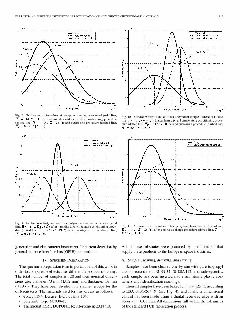
Fig. 8. Surface resistivity values of ten epoxy samples as received (solid line,�R =5:62 E+16 ), after humidity and temperature conditioning procedure(dotted line, �R = 3:48 E+16 ) and outgassing procedure (dashed line,�R = 8:95 E+16 ).
Fig. 9. Surface resistivity values of ten polyimide samples as received (solidline, �R =1:72E+17), after humidity and temperature conditioning proce-dure (dotted line, �R =9:72E+16) and outgassing procedure (dashed line,�R = 2:74 E+17 ).
generation and electrometer instrument for current detection bygeneral purpose interface bus (GPIB) connection.
IV. SPECIMEN PREPARATION
The specimen preparation is an important part of this work inorder to compare the effects after different type of conditioning.The total number of samples is 120 and their nominal dimen-sions are: diameter 70 mm ( 0.2 mm) and thickness 1.6 mm( 10 ). They have been divided into smaller groups for thedifferent tests. The materials used for this test are as follows:
• epoxy FR-4, Duraver E-Cu quality 104;• polymide, Type N7000–1;• Thermount 55RT, DUPONT, Reinforcement 2.0N710.
Fig. 10. Surface resistivity values of ten Thermount samples as received (solidline, �R =3:32E+16), after humidity and temperature conditioning proce-dure (dotted line, �R =6:64E+16) and outgassing procedure (dashed line,�R = 5:55 E+16 ).
Fig. 11. Surface resistivity values of ten epoxy samples as received (solid line,�R = 7:27 E+16 ), after corona discharge procedure (dotted line, �R =
7:22 E+16 ).
All of these substrates were procured by manufacturers thatsupply these products to the European space industries.
A. Sample Cleaning, Marking, and Baking
Samples have been cleaned one by one with pure isopropylalcohol according to ECSS–Q–70–08A [12] and, subsequently,each sample has been inserted into small sterile plastic con-tainers with identification markings.
Then all samples have been baked for 4 h at 125 C accordingto ESA STM-267 [9] (see Fig. 4), and finally a dimensionalcontrol has been made using a digital receiving gage with anaccuracy 0.01 mm. All dimensions fall within the tolerancesof the standard PCB fabrication process.
120 IEEE TRANSACTIONS ON ELECTRONICS PACKAGING MANUFACTURING, VOL. 30, NO. 2, APRIL 2007
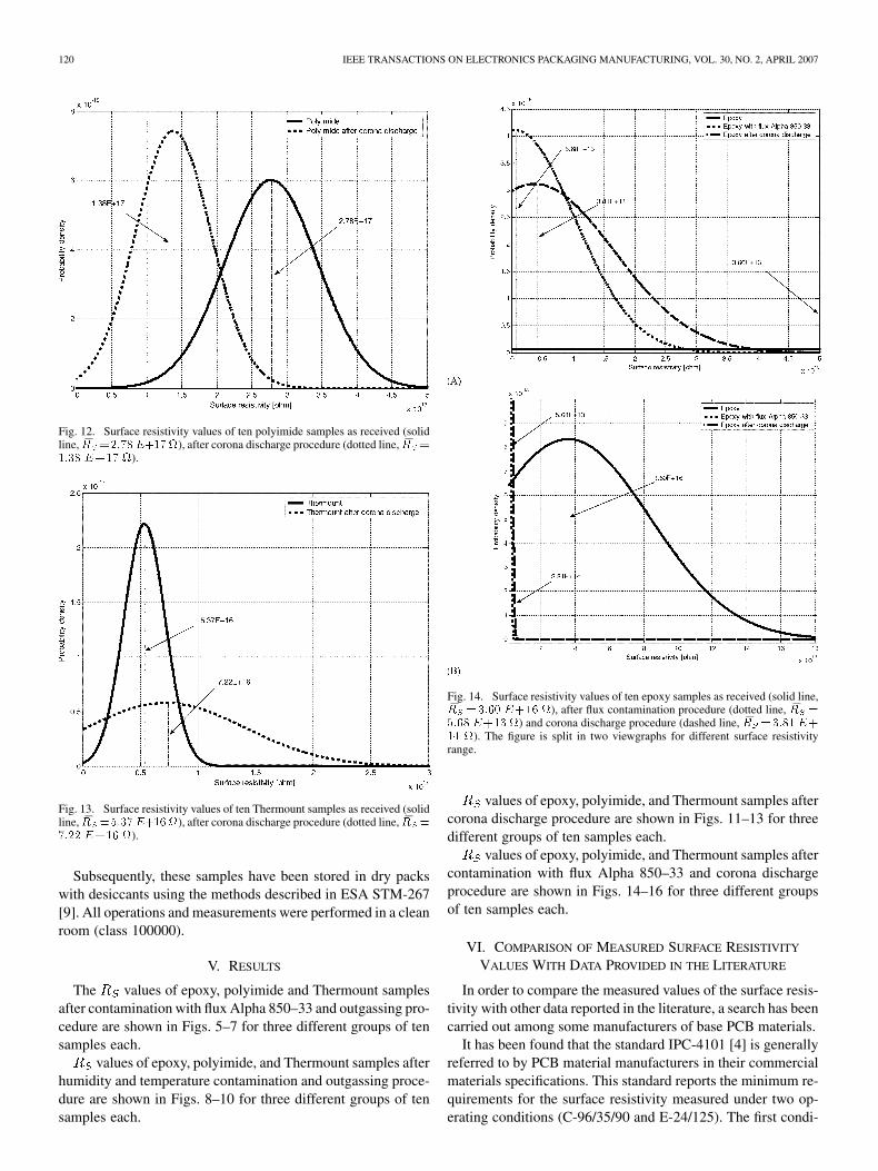
Fig. 12. Surface resistivity values of ten polyimide samples as received (solidline, �R =2:78E+17), after corona discharge procedure (dotted line, �R =
1:38 E+17 ).
Fig. 13. Surface resistivity values of ten Thermount samples as received (solidline, �R =5:37E+16), after corona discharge procedure (dotted line, �R =
7:22 E+16 ).
Subsequently, these samples have been stored in dry packswith desiccants using the methods described in ESA STM-267[9]. All operations and measurements were performed in a cleanroom (class 100000).
V. RESULTS
The values of epoxy, polyimide and Thermount samplesafter contamination with flux Alpha 850–33 and outgassing pro-cedure are shown in Figs. 5–7 for three different groups of tensamples each.
values of epoxy, polyimide, and Thermount samples afterhumidity and temperature contamination and outgassing proce-dure are shown in Figs. 8–10 for three different groups of tensamples each.
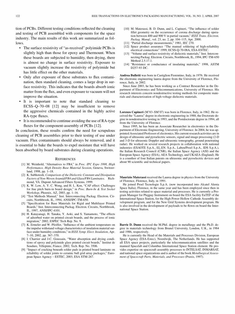
Fig. 14. Surface resistivity values of ten epoxy samples as received (solid line,�R =3:60 E+16 ), after flux contamination procedure (dotted line, �R =
5:68E+13 ) and corona discharge procedure (dashed line, �R =3:81E+
14 ). The figure is split in two viewgraphs for different surface resistivityrange.
values of epoxy, polyimide, and Thermount samples aftercorona discharge procedure are shown in Figs. 11–13 for threedifferent groups of ten samples each.
values of epoxy, polyimide, and Thermount samples aftercontamination with flux Alpha 850–33 and corona dischargeprocedure are shown in Figs. 14–16 for three different groupsof ten samples each.
VI. COMPARISON OF MEASURED SURFACE RESISTIVITY
VALUES WITH DATA PROVIDED IN THE LITERATURE
In order to compare the measured values of the surface resis-tivity with other data reported in the literature, a search has beencarried out among some manufacturers of base PCB materials.
It has been found that the standard IPC-4101 [4] is generallyreferred to by PCB material manufacturers in their commercialmaterials specifications. This standard reports the minimum re-quirements for the surface resistivity measured under two op-erating conditions (C-96/35/90 and E-24/125). The first condi-
BULLETTI et al.: SURFACE RESISTIVITY CHARACTERIZATION OF NEW PRINTED CIRCUIT BOARD MATERIALS 121
Fig. 15. Surface resistivity values of ten polyimide samples as received (solidline, �R = 1:76 E+17 ), after flux contamination procedure (dotted line,�R = 5:03 E+13 ) and corona discharge procedure (dashed line, �R =
7:20 E+13 ). The figure is split in two viewgraphs for different surface re-sistivity range.
tion has also been adopted in our experiment, but with a highertemperature (70 C instead of 35 C), and so the latter can beconsidered a more stressful condition. The test method for mea-suring the surface resistivity is the IPC-TM-650, n. 2.5.17.1 [13]and it refers to [14], which has been also adopted for our mea-surements.
Table I reports the IPC-4101 [4] minimum values, the meanexperimental values acquired in this study, and the values pro-vided by three main PCB material manufacturers (Arlon, Isola,and Nelco). Each value is referred to a specific type of FR4 orpolyimide that is reported in Table I.
VII. DISCUSSION OF RESULTS
According to previous experimental data we can analyze thevariations of the surface resistivity.
• For the samples as received from manufacturer, polyimidematerial shows the highest values of surface resistivity re-spect to Thermount and epoxy.
Fig. 16. Surface resistivity values of ten Thermount samples as received (solidline, �R = 1:88 E+16 ), after flux contamination procedure (dotted line,�R = 1:08 E+15 ) and corona discharge procedure (dashed line, �R =
2:00 E+15 ).
TABLE ICOMPARISON BETWEEN IPC 4101 [5] VALUES FOR EPOXY, POLYIMIDE,
AND THERMOUNT MATERIALS, MANUFACTURERS VALUES FOUND IN THE
LITERATURE AND THE EXPERIMENTAL VALUES FROM THE PRESENT STUDY.THE CONDITIONING IS THE SAME STANDARD C-96/35/90 FOR ALL CASES
• Contamination with flux Alpha 850–33 type RA caused adecrease of surface resistivity, for all materials treated, upto four orders of magnitudes (see Figs. 5–7 and 14–16).
• Humidity and temperature variation and corona dischargedid not modify significantly the values of surface resistivitywith respect to the values measured for samples as received(see Figs. 8–10 and 11–13).
• All materials showed an increase of surface resistivity afteroutgassing (see Figs. 5–7 and 8–10).
• Polyimide material showed the lowest values of surfaceresistivity, after all test procedures, with respect to the othermaterials.
We notice that the analyses of the surface resistivity of the varia-tions is significant because the averaged values are three or fourorders of magnitude greater than the standard deviation.
VIII. CONCLUSION
The aim of this work was to study the surface resistivity vari-ation for three types of substrate material used for the fabrica-
122 IEEE TRANSACTIONS ON ELECTRONICS PACKAGING MANUFACTURING, VOL. 30, NO. 2, APRIL 2007
tion of PCBs. Different testing conditions reflected the cleaningand testing of PCB assembled with components for the spaceindustry. The main results of this work are summarized as fol-lows.
• The surface resistivity of “as-received” polyimide PCBs isslightly high than those for epoxy and Thermount. Whenthese boards are subjected to humidity, then drying, thereis almost no change in surface resistivity. Exposure tovacuum slightly increase the resistivity of polyimide buthas little effect on the other materials.
• Only after exposure of these substrates to flux contami-nation, then standard cleaning, comes a large drop in sur-face resistivity. This indicates that the boards absorb ionicmatter from the flux, and even exposure to vacuum will notimprove the situation.
• It is important to note that standard cleaning toECSS–Q–70–08 [12] may be insufficient to removethe aggressive chemicals contained in the highly activeRA-type fluxes.
• It is recommended to continue avoiding the use of RA-typefluxes for the component-assembly of PCBs [12].
In conclusion, these results confirm the need for scrupulouscleaning of PCB assemblies prior to their testing of use undervacuum. Flux contaminants should always be removed, and itis essential to bake the boards to expel moisture that will havebeen absorbed by board substrates during cleaning operations.
REFERENCES
[1] M. Weinhold, “Alternatives to FR4,” in Proc. IPC Expo 1998, HighPerformance, High Density Base Material Session, Geneva, Switzer-land, 1998, pp. 1–18.
[2] K. Subhotosh, Comparison of the Dielectric Constant and DissipationFactors of Non-Woven Aramid/FR4 and Glass/FR4 Laminates. Rich-mond, VA: Dupont Advanced Fibers Systems, 1999.
[3] K. W. Low, A. Y. C. Wong, and H. L. Kon, “CAF effect: Challengesfor fine pitch burn-in board design,” in Proc. Burn-In & Test SocketWorkshop, Phoenix, AZ, 2003, pp. 1–16.
[4] “Test Methods Manual,” Inst. Interconnecting Packag. Electron. Cir-cuits, Northbrook, IL, 1994, ANSI/IPC-TM-650.
[5] “Specification for Base Materials for Rigid and Multilayer PrintedBoards,” Inst. Interconnecting Packag. Electron. Circuits, Northbrook,IL, 1997, ANSI/IPC-4101.
[6] H. Katayanagi, H. Tanaka, Y. Aoki, and S. Yamamoto, “The effectsof adsorbed water on printed circuit boards, and the process of ionicmigration,” 2002, ESPEC Tech Rep. No. 9.
[7] K. Ermeler and W. Pfeiffer, “Influence of the ambient temperature onthe impulse withstand voltage characteristics of insulation material sur-face under humidity conditions,” in IEEE Symp. Elect. Insulation, Apr.7–10, 2002, pp. 367–370.
[8] I. Charrier and J-C. Goussain, “Water absorption and drying condi-tions of epoxy and polyimide glass printed circuit boards,” Institut deSoudure, Villepinte, France, 2002, Tech. Rep. No. 3506.
[9] “Impact of cracking beneath solder pads in printed board laminate onreliability of solder joints to ceramic ball grid array packages,” Euro-pean Space Agency – ESTEC, 2003, ESA STM-267.
[10] M. Materassi, B. D. Dunn, and L. Capineri, “The influence of solderfillet geometry on the occurrence of corona discharge during opera-tion between 400 and 900 V in partial vacuum,” IEEE Trans. Electron.Packag. Manuf., vol. 23, no. 2, pp. 104–115, Apr. 2000.
[11] “Partial discharge measurements,” 1981, IEC 270.[12] Space product assurance “The manual soldering of high-reliability
electrical connections” 1999, ECSS-Q-70-08A, ESA-ESTEC.[13] “Volume and surface resistivity of dielectric materials,” Inst. Intercon-
necting Packag. Electron. Circuits, Northbrook, IL, 1994, IPC-TM-650Method 2.5.17.1.
[14] “Resistance or conductance of insulating materials,” 1998, ASTMD257-93 DC.
Andrea Bulletti was born in Castiglion Fiorentino, Italy, in 1976. He receivedthe electronic engineering laurea degree from the University of Florence, Flo-rence, Italy, in 2002.
Since June 2003, he has been working as a Contract Researcher in the De-partment of Electronics and Telecommunications, University of Florence. Hisresearch interests concern nondestructive testing methods for composite mate-rials and characterization of high-voltage dielectric materials.
Lorenzo Capineri (M’83–SM’07) was born in Florence, Italy, in 1962. He re-ceived the “Laurea” degree in electronic engineering in 1988, the Doctorate de-gree in nondestructive testing in 1993, and the Postdoctorate degree in 1994, allfrom the University of Florence.
Since 1995, he has been an Associate Researcher in electronics in the De-partment of Electronic Engineering, University of Florence. In 2004, he was ap-pointed Associated Professor of electronics. His current research activities are indesign of ultrasonic and pyroelectric sensors, signal and image processing (2-Dand 3-D for ultrasonic Doppler and ultrasonic tomography, ground penetratingradar). He worked on several research projects in collaboration with nationalindustries (ESAOTE S.p.A., EL.EN. S.p.A., Laben/Proel S.p.A., IDS S.p.A.),the Italian Research Council (CNR), the Italian Space Agency (ASI) and theEuropean Space Agency (ESA), AEA Technology, and UKAEA (England). Heis a coauthor of four Italian patents on ultrasonic and pyroelectric devices andabout 90 scientific and technical papers.
Maurizio Materassi received the Laurea degree in physics from the Universityof Florence, Florence, Italy, in 1991.
He joined Proel Tecnologie S.p.A. (now incorporated into Alcatel AleniaSpace Italia), Florence, in the same year and has been employed since then intesting activities related to space material and processes. He is currently a Pro-gram Manager for Plegpay Instrument on board the ESA facility EuTEF of theInternational Space Station, for the High Power Hollow Cathode Assembly de-velopment program, and for the New Grid Systems development program. Heis also involved in the development of payloads to be flown on board the Inter-national Space Station.
Barrie D. Dunn received the M.Phil. degree in metallurgy and the Ph.D. de-gree in materials technology from Brunel University, London, U.K., in 1984and 1986, respectively.
He is currently the Head of the Materials and Processes Division, EuropeanSpace Agency (ESA-Estec), Noordwijk, The Netherlands. He has supportedall ESA space projects, particularly the telecommunication satellites and themanned Spacelab and Columbus International Space Station element. He pro-vides expertise on spacecraft assembly processes to INTELSAT, INMARSAT,and national space organizations and is author of the book Metallurgical Assess-ment of Spacecraft Parts, Materials, and Processes (Praxis, 1997).