Embed Size (px)
Citation preview
IEEE TRANSACTIONS ON NUCLEAR SCIENCE, VOL. 55, NO. 4, AUGUST 2008 1833
Radiation Effects in MOS OxidesJames R. Schwank, Fellow, IEEE, Marty R. Shaneyfelt, Fellow, IEEE, Daniel M. Fleetwood, Fellow, IEEE,James A. Felix, Member, IEEE, Paul E. Dodd, Senior Member, IEEE, Philippe Paillet, Senior Member, IEEE,
and Véronique Ferlet-Cavrois, Senior Member, IEEE
Abstract—Electronic devices in space environments can containnumerous types of oxides and insulators. Ionizing radiation caninduce significant charge buildup in these oxides and insulatorsleading to device degradation and failure. Electrons and protons inspace can lead to radiation-induced total-dose effects. The two pri-mary types of radiation-induced charge are oxide-trapped chargeand interface-trap charge. These charges can cause large radia-tion-induced threshold voltage shifts and increases in leakage cur-rents. Two alternate dielectrics that have been investigated for re-placing silicon dioxide are hafnium oxides and reoxidized nitridedoxides (RNO). For advanced technologies, which may employ al-ternate dielectrics, radiation-induced voltage shifts in these insula-tors may be negligible. Radiation-induced charge buildup in par-asitic field oxides and in SOI buried oxides can also lead to devicedegradation and failure. Indeed, for advanced commercial tech-nologies, the total-dose hardness of ICs is normally dominated byradiation-induced charge buildup in either parasitic field oxidesand/or SOI buried oxides. Heavy ions in space can also degrade theoxides in electronic devices through several different mechanismsincluding single-event gate rupture, reduction in device lifetime,and large voltage shifts in power MOSFETs.
Index Terms—Aging, MOS devices, oxide breakdown, powerMOSFETs, radiation effects, silicon-on-insulator, total doseeffects.
I. INTRODUCTION
F ROM MOSFETs to bipolar ICs, oxides and insulators arekey components of many electronic devices. Ionizing radi-
ation can induce significant charge buildup in these oxides andinsulators leading to device degradation and failure. In spacesystems (and other harsh radiation environments, e.g., high-en-ergy particle accelerators), exposure to high fluxes of electronsand protons can significantly reduce system lifetime due to totalionizing dose. Over the last thirty years, the effects of total ion-izing dose on radiation-induced charge buildup in oxides havebeen investigated in detail. In addition to total ionizing dose ef-fects, the energetic particles of space can also induce degrada-tion by other mechanisms. For example, the heavy ions in space
Manuscript received November 6, 2007; revised May 16, 2008. Current ver-sion published September 19, 2008. This work was supported by the DefenseThreat Reduction Agency under DTRA IACRO 07-4196I and the U. S. Depart-ment of Energy. Sandia is a multiprogram laboratory operated by Sandia Corpo-ration, a Lockheed Martin Company, for the U.S. Department of Energy’s Na-tional Nuclear Security Administration under Contract DE-AC04-94AL85000.
J. R. Schwank, M. R. Shaneyfelt, J. A. Felix, and P. E. Dodd are withSandia National Laboratories, Albuquerque, NM 87185 USA (e-mail:[email protected]).
D. M. Fleetwood is with Vanderbilt University, Nashville, TN 37235 USA.P. Paillet and V. Ferlet-Cavrois are with CEA-DIF, 91680 Bruyères-le-Châtel,
France.Color versions of one or more of the figures in this paper are available online
at http://ieeexplore.ieee.org.Digital Object Identifier 10.1109/TNS.2008.2001040
environments can reduce long-term reliability and lead to cata-strophic device failure.
In this paper, we review the effects of radiation on oxide-in-duced device degradation and failure. The effects of total ion-izing dose radiation-induced charge buildup in and alter-native high-k gate dielectrics, field isolation, and silicon-on-in-sulator (SOI) buried oxides, and oxide hardening techniques arefirst reviewed. The effects of aging and pre-irradiation elevatedtemperature stress on MOS and bipolar radiation response arealso discussed. After that, the mechanisms and properties ofheavy ion-induced single-event gate rupture (SEGR) will be dis-cussed, followed by a brief discussion of the effects of heavy-ionexposure on long-term reliability.
II. TOTAL-DOSE EFFECTS
A. Overview
High-energy electrons (secondary electrons generated byphoton interactions or electrons present in the environment)and protons can ionize atoms, generating electron-hole pairs.As long as the energies of the electrons and holes generatedare higher than the minimum energy required to create an elec-tron-hole pair, they can in turn generate additional electron-holepairs. In this manner, a single, high-energy incident photon,electron, or proton can create thousands of electron-hole pairs.
When an MOS transistor is exposed to high-energy ion-izing irradiation, electron-hole pairs are created in the oxide.Electron-hole pair generation in the oxide leads to almost alltotal dose effects. The generated carriers induce the buildup ofcharge, which can lead to device degradation. The mechanismsby which device degradation occurs are depicted in Fig. 1.Fig. 1 is a plot of an MOS band diagram for a p-substratecapacitor with a positive applied gate bias. Immediately afterelectron-hole pairs are created, most of the electrons willrapidly drift (within picoseconds) toward the gate and holeswill drift toward the Si/ interface. However, even beforethe electrons leave the oxide, some of the electrons will recom-bine with holes. The fraction of electron-hole pairs that escaperecombination is called the electron-hole yield or charge yield.Those holes which escape “initial” recombination will transportthrough the oxide toward the Si/ interface by hoppingthrough localized states in the oxide. As the holes approachthe interface, some fraction will be trapped, forming a positiveoxide-trap charge. It is believed that hydrogen ions (protons)are likely released as holes “hop” through the oxide or as theyare trapped near the Si/ interface. The hydrogen ions canalso drift to the Si/ where they may react to form interfacetraps. At threshold, interface traps are predominantly positively
0018-9499/$25.00 © 2008 IEEE
Authorized licensed use limited to: ELETTRONICA E INFORMATICA PADOVA. Downloaded on July 30, 2009 at 21:03 from IEEE Xplore. Restrictions apply.
1834 IEEE TRANSACTIONS ON NUCLEAR SCIENCE, VOL. 55, NO. 4, AUGUST 2008
Fig. 1. Band diagram of an MOS capacitor with a positive gate bias. Illustratedare the main processes for radiation-induced charge generation.
charged for p-channel transistors and negatively charged forn-channel transistors.
In addition to oxide-trapped charge and interface-trap chargebuildup in gate oxides, charge buildup will also occur in otheroxides including field oxides, silicon-on-insulator (SOI) buriedoxides, and alternate dielectrics. The radiation-induced chargebuildup in these insulators can cause device degradation and cir-cuit failure. Positive charge trapping in the gate oxide can invertthe channel interface causing leakage current to flow in the OFFstate condition ( ). This will result in an increase inthe static power supply current of an IC and may also cause ICfailure. In a similar fashion, positive charge buildup in field andSOI buried oxides can cause large increases in IC static powersupply leakage current (caused by parasitic leakage paths in thetransistor). In fact, for advanced ICs with very thin gate oxides,radiation-induced charge buildup in field oxides and SOI buriedoxides normally dominates the radiation-induced degradation ofICs. Large concentrations of interface-trap charge can decreasethe mobility of carriers and increase the threshold voltage ofn-channel MOS transistors. These effects will tend to decreasethe drive of transistors, degrading timing parameters of an IC.In the rest of this section, we present the details of oxide-trapand interface-trap charge buildup in MOS transistors.
B. Charge Yield
If an electric field exists across the oxide of an MOS tran-sistor, once generated, electrons in the conduction band andholes in the valence band will immediately begin to transportin opposite directions. Electrons are extremely mobile in sil-icon dioxide and are normally swept out of silicon dioxide inpicoseconds [1], [2]. However, even before the electrons canleave the oxide, some fraction of the electrons will recombinewith holes in the oxide valence band. This is referred to as initialrecombination. The amount of initial recombination is highlydependent on the electric field in the oxide and the energy andtype of incident particle [3]. In general, strongly ionizing parti-cles form dense columns of charge where the recombination rateis relatively high. On the other hand, weakly ionizing particlesgenerate relatively isolated charge pairs, and the recombinationrate is lower [3]. The dependence of initial recombination onthe electric field strength in the oxide for low-energy protons,
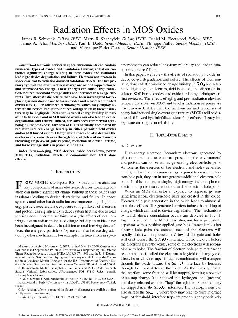
Fig. 2. The fraction of holes that escape initial recombination (charge yield)for x rays, low-energy protons, gamma rays, and alpha particles. (After [4] and[5].)
alpha particles, gamma rays (Co-60) , and x rays is illustratedin Fig. 2 [4], [5]. Plotted in Fig. 2 is the fraction of unrecom-bined holes (charge yield) versus electric field in the oxide. Thedata for the Co-60 and 10-keV x-ray curves were taken from [5].The other two curves were taken from [4]. For all particles, asthe electric field strength increases, the probability that a holewill recombine with an electron decreases, and the fraction ofunrecombined holes increases. Taking into account the effectsof hole yield and electron-hole pair generation, the total numberof holes generated in the oxide (not including dose enhancementeffects [3], [4] that escape initial recombination, , is given by[4]
(1)
where is the hole yield as a function of oxide electricfield, is the dose, and is the oxide thickness (in unitsof cm). is a material-dependent parameter giving the initialcharge pair density per rad of dose (per rad for [4]).
C. Oxide Traps
Holes generated in the oxide transport much slower throughthe lattice than electrons [1]. In the presence of an electric field,holes can transport to either the gate/ (negatively appliedgate bias) or the Si/ interface (positively applied gate bias).Due to its charge, as a hole moves through the it causes adistortion of the local potential field of the lattice. Thislocal distortion increases the trap depth at the localized site,which tends to confine the hole to its immediate vicinity. Thus,in effect, the hole tends to trap itself at the localized site. Thecombination of the charged carrier (hole) and its strain field isknown as a polaron [6]. As a hole transports through the lattice,the distortion follows the hole. Hence, holes transport through
by “polaron hopping” [4], [7], [8]. Polarons increase theeffective mass of the holes and decrease their mobility. Polaron
Authorized licensed use limited to: ELETTRONICA E INFORMATICA PADOVA. Downloaded on July 30, 2009 at 21:03 from IEEE Xplore. Restrictions apply.
SCHWANK et al.: RADIATION EFFECTS IN MOS OXIDES 1835
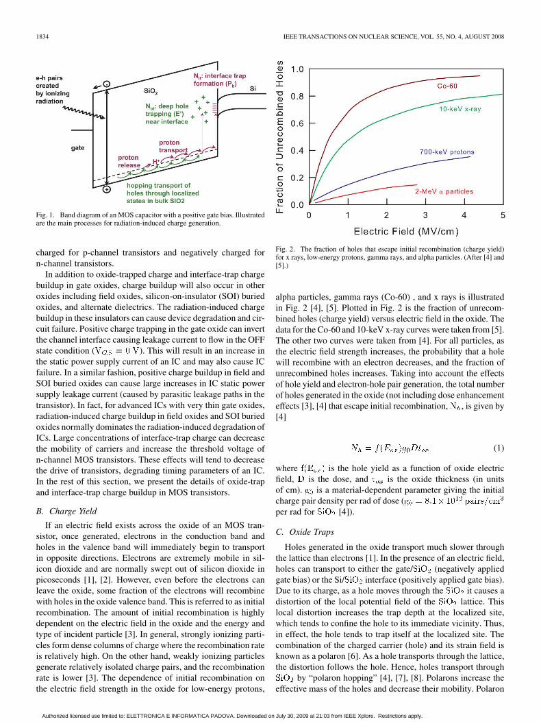
Fig. 3. Electric field dependence of �V versus electric field. Shown arethe measured data (circles) and the measured data corrected for charge yield(squares). (After [10].)
hopping makes hole transport dispersive (i.e., hole transport oc-curs over many decades in time after a radiation pulse) and verytemperature and oxide thickness dependent [4], [7], [8].
With the application of a positive gate bias, holes transportto the Si/ interface. Close to the interface there are alarge number of oxygen vacancies due to the out-diffusionof oxygen in the oxide [9] and lattice mismatch at the sur-face. These oxygen vacancies can act as trapping centers.As holes approach the interface, some fraction of the holeswill become trapped. The number of holes that are trapped isgiven by the capture cross-section near the interface, which isdependent on the applied field and is very device fabricationdependent, with only a few percent of the holes being trappedin hardened oxides to as much as 50 to 100% for soft oxides.The positive charge associated with trapped holes causes anegative threshold-voltage shift in both n- and p-channel MOStransistors.
The effect of the capture cross-section on trapped-holebuildup can be observed in the electric field dependence of thebuildup of oxide traps shortly after irradiation. Fig. 3 is a plotof the threshold-voltage shift due to oxide-trap charge, ,versus oxide electric field [10]. The circles are the measureddata, the squares are the measured data adjusted for chargeyield, and the solid line is a plot of . For electric fieldsgreater than 0.5 V/cm, adjusted for charge yield de-creases with approximately an electric field dependence.This is the same electric field dependence as is observed forthe hole capture cross-section near the Si/ interface [3],[11]–[15]. This indicates that the field dependence of oxide-trapcharge buildup is determined primarily by the hole capturecross-section.
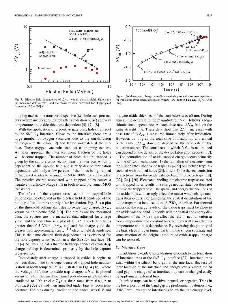
Immediately after charge is trapped in oxides it begins tobe neutralized. The time dependence of trapped-hole neutral-ization at room temperature is illustrated in Fig. 4 [16], wherethe voltage shift due to oxide-trap charge, , is plottedversus time for hardened n-channel polysilicon gate transistorsirradiated to 100 at dose rates from 6 to0.05 and then annealed under bias at room tem-perature. The bias during irradiation and anneal was 6 V and
Fig. 4. Oxide-trapped charge neutralization during anneal at room temperaturefor transistors irradiated at dose rates from 6�10 to 0.05 rad(SiO )=s. (After[16].)
the gate oxide thickness of the transistors was 60 nm. Duringanneal, the decrease in the magnitude of follows a loga-rithmic time dependence. At each dose rate, falls on thesame straight line. These data show that increases withdose rate if is measured immediately after irradiation.However, as long as the total time of irradiation and annealis the same, dose not depend on the dose rate of theradiation source. The actual rate at which is neutralizedcan depend on the details of the device fabrication process [17].
The neutralization of oxide-trapped charge occurs primarilyby one of two mechanisms: 1) the tunneling of electrons fromthe silicon into either oxide traps [17]–[22] or electron traps as-sociated with trapped holes [23], and/or 2) the thermal emissionof electrons from the oxide valence band into oxide traps [18],[22], [24]–[26]. Electron tunneling into electron traps associatedwith trapped holes results in a charge neutral state, but does notremove the trapped hole. The spatial and energy distributions ofthe oxide traps will strongly affect the rate at which charge neu-tralization occurs. For tunneling, the spatial distribution of theoxide traps must be close to the Si/ interface. For thermalemission, the energy levels of the oxide traps must be close tothe oxide valence band. Not only will the spatial and energy dis-tributions of the oxide traps affect the rate of neutralization atroom temperature and constant bias, but they will also affect itstemperature and bias dependence. By reversing the polarity ofthe bias, electrons can tunnel back into the silicon substrate andsome fraction of the original amount of oxide-trapped chargecan be restored.
D. Interface Traps
In addition to oxide traps, radiation also leads to the formationof interface traps at the Si/ interface [27]. Interface trapsexist within the silicon band gap at the interface. Because oftheir location at the interface and energy levels within the Siband gap, the charge of an interface trap can be changed easilyby applying an external bias.
Interface traps can be positive, neutral, or negative. Traps inthe lower portion of the band gap are predominantly donors; i.e.,if the Fermi level at the interface is below the trap energy level,
Authorized licensed use limited to: ELETTRONICA E INFORMATICA PADOVA. Downloaded on July 30, 2009 at 21:03 from IEEE Xplore. Restrictions apply.
1836 IEEE TRANSACTIONS ON NUCLEAR SCIENCE, VOL. 55, NO. 4, AUGUST 2008
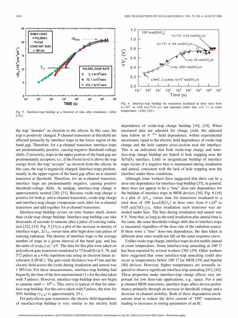
Fig. 5. Interface-trap buildup as a function of time after irradiation. (After[33].)
the trap “donates” an electron to the silicon. In this case, thetrap is positively charged. P-channel transistors at threshold areaffected primarily by interface traps in the lower region of theband gap. Therefore, for a p-channel transistor, interface trapsare predominantly positive, causing negative threshold-voltageshifts. Conversely, traps in the upper portion of the band gap arepredominantly acceptors; i.e., if the Fermi level is above the trapenergy level, the trap “accepts” an electron from the silicon. Inthis case, the trap is negatively charged. Interface traps predom-inantly in the upper region of the band gap affect an n-channeltransistor at threshold. Therefore, for an n-channel transistor,interface traps are predominantly negative, causing positivethreshold-voltage shifts. At midgap, interface-trap charge isapproximately neutral [28]–[31]. Because oxide-trap charge ispositive for both p- and n-channel transistors, oxide-trap chargeand interface-trap charge compensate each other for n-channeltransistors and add together for p-channel transistors.
Interface-trap buildup occurs on time frames much slowerthan oxide-trap charge buildup. Interface-trap buildup can takethousands of seconds to saturate after a pulse of ionizing radia-tion [32], [33]. Fig. 5 [33] is a plot of the increase in density ofinterface-traps, , versus time after high-dose-rate pulses ofionizing radiation. The density of interface traps is the averagenumber of traps in a given interval of the band gap, and hasthe units of -eV. The data for this plot were taken onpolysilicon gate transistors irradiated to 75 krad(Si) in 5, 70, and572 pulses at a 4-Hz repetition rate using an electron linear ac-celerator (LINAC). The gate oxide thickness was 47 nm and theelectric field across the oxide during irradiation and anneal was1 MV/cm. For these measurements, interface-trap buildup hadbegun by the time of the first measurement (1 s for the data takenwith 5 pulses). However, interface-trap buildup does not beginto saturate until . This curve is typical of that for inter-face-trap buildup. For the curve taken with 5 pulses, the time for50% buildup ( ) is approximately 35 s.
For polysilicon-gate transistors, the electric field dependenceof interface-trap buildup is very similar to the electric field
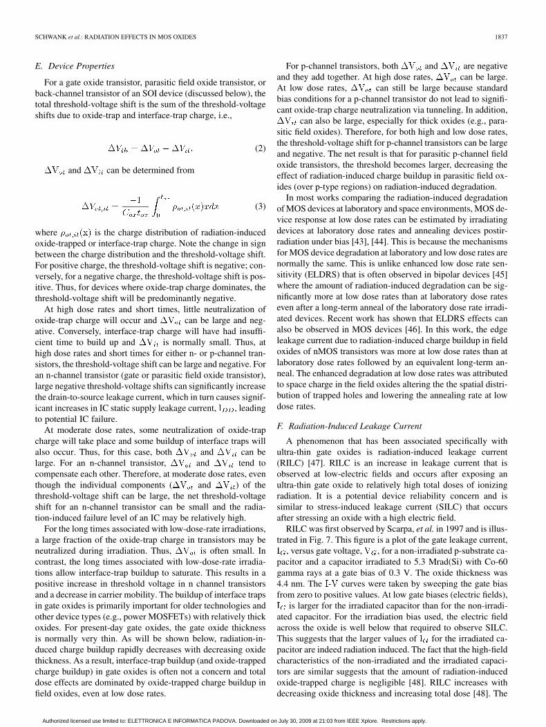
Fig. 6. Interface-trap buildup for transistors irradiated at dose rates from6�10 to 0.05 rad(SiO )=s and annealed under bias (+6 V) at roomtemperature. (After [16].)
dependence of oxide-trap charge buildup [10], [34]. Whenmeasured data are adjusted for charge yield, the adjusteddata follow an field dependence, within experimentaluncertainty equal to the electric field dependence of oxide-trapcharge and the hole capture cross-section near the interface.This is an indication that both oxide-trap charge and inter-face-trap charge buildup are linked to hole trapping near theSi/ interface. Little or insignificant buildup of interfacetraps occurs if a negative bias is maintained during irradiationand anneal, consistent with the lack of hole trapping near theinterface under these conditions.
Although some workers have suggested that there can be adose rate dependence for interface-trap buildup [35], in general,there does not appear to be a “true” dose-rate dependence forthe buildup of interface traps in MOS devices [16]. Fig. 6 [16]is a plot of versus time for transistors irradiated to atotal dose of 100 at dose rates from 6 to0.05 . After irradiation each transistor was an-nealed under bias. The bias during irradiation and anneal was6 V. Note that, as long as the total irradiation plus anneal time isthe same, the same threshold-voltage shift due to interface trapsis measured, regardless of the dose rate of the radiation source.If there were a “true” dose-rate dependence, the data taken atdifferent dose rates would not fall on the same response curve.
Unlike oxide-trap charge, interface traps do not readily annealat room temperature. Some interface-trap annealing at 100has been reported by several workers [36]–[39]. Other workershave suggested that some interface-trap annealing could alsooccur at temperatures below 100 for MOS [39] and bipolar[40] devices. However, higher temperatures are normally re-quired to observe significant interface-trap annealing [41], [42].These properties make interface-trap charge effects very im-portant for low dose-rate applications, e.g., space. For n andp-channel MOS transistors, interface traps affect device perfor-mance primarily through an increase in threshold voltage and adecrease in channel mobility. Both of these degradation mech-anisms tend to reduce the drive current of “ON” transistors,leading to increases in timing parameters of an IC.
Authorized licensed use limited to: ELETTRONICA E INFORMATICA PADOVA. Downloaded on July 30, 2009 at 21:03 from IEEE Xplore. Restrictions apply.
SCHWANK et al.: RADIATION EFFECTS IN MOS OXIDES 1837
E. Device Properties
For a gate oxide transistor, parasitic field oxide transistor, orback-channel transistor of an SOI device (discussed below), thetotal threshold-voltage shift is the sum of the threshold-voltageshifts due to oxide-trap and interface-trap charge, i.e.,
(2)
and can be determined from
(3)
where is the charge distribution of radiation-inducedoxide-trapped or interface-trap charge. Note the change in signbetween the charge distribution and the threshold-voltage shift.For positive charge, the threshold-voltage shift is negative; con-versely, for a negative charge, the threshold-voltage shift is pos-itive. Thus, for devices where oxide-trap charge dominates, thethreshold-voltage shift will be predominantly negative.
At high dose rates and short times, little neutralization ofoxide-trap charge will occur and can be large and neg-ative. Conversely, interface-trap charge will have had insuffi-cient time to build up and is normally small. Thus, athigh dose rates and short times for either n- or p-channel tran-sistors, the threshold-voltage shift can be large and negative. Foran n-channel transistor (gate or parasitic field oxide transistor),large negative threshold-voltage shifts can significantly increasethe drain-to-source leakage current, which in turn causes signif-icant increases in IC static supply leakage current, , leadingto potential IC failure.
At moderate dose rates, some neutralization of oxide-trapcharge will take place and some buildup of interface traps willalso occur. Thus, for this case, both and can belarge. For an n-channel transistor, and tend tocompensate each other. Therefore, at moderate dose rates, eventhough the individual components ( and ) of thethreshold-voltage shift can be large, the net threshold-voltageshift for an n-channel transistor can be small and the radia-tion-induced failure level of an IC may be relatively high.
For the long times associated with low-dose-rate irradiations,a large fraction of the oxide-trap charge in transistors may beneutralized during irradiation. Thus, is often small. Incontrast, the long times associated with low-dose-rate irradia-tions allow interface-trap buildup to saturate. This results in apositive increase in threshold voltage in n channel transistorsand a decrease in carrier mobility. The buildup of interface trapsin gate oxides is primarily important for older technologies andother device types (e.g., power MOSFETs) with relatively thickoxides. For present-day gate oxides, the gate oxide thicknessis normally very thin. As will be shown below, radiation-in-duced charge buildup rapidly decreases with decreasing oxidethickness. As a result, interface-trap buildup (and oxide-trappedcharge buildup) in gate oxides is often not a concern and totaldose effects are dominated by oxide-trapped charge buildup infield oxides, even at low dose rates.
For p-channel transistors, both and are negativeand they add together. At high dose rates, can be large.At low dose rates, can still be large because standardbias conditions for a p-channel transistor do not lead to signifi-cant oxide-trap charge neutralization via tunneling. In addition,
can also be large, especially for thick oxides (e.g., para-sitic field oxides). Therefore, for both high and low dose rates,the threshold-voltage shift for p-channel transistors can be largeand negative. The net result is that for parasitic p-channel fieldoxide transistors, the threshold becomes larger, decreasing theeffect of radiation-induced charge buildup in parasitic field ox-ides (over p-type regions) on radiation-induced degradation.
In most works comparing the radiation-induced degradationof MOS devices at laboratory and space environments, MOS de-vice response at low dose rates can be estimated by irradiatingdevices at laboratory dose rates and annealing devices postir-radiation under bias [43], [44]. This is because the mechanismsfor MOS device degradation at laboratory and low dose rates arenormally the same. This is unlike enhanced low dose rate sen-sitivity (ELDRS) that is often observed in bipolar devices [45]where the amount of radiation-induced degradation can be sig-nificantly more at low dose rates than at laboratory dose rateseven after a long-term anneal of the laboratory dose rate irradi-ated devices. Recent work has shown that ELDRS effects canalso be observed in MOS devices [46]. In this work, the edgeleakage current due to radiation-induced charge buildup in fieldoxides of nMOS transistors was more at low dose rates than atlaboratory dose rates followed by an equivalent long-term an-neal. The enhanced degradation at low dose rates was attributedto space charge in the field oxides altering the the spatial distri-bution of trapped holes and lowering the annealing rate at lowdose rates.
F. Radiation-Induced Leakage Current
A phenomenon that has been associated specifically withultra-thin gate oxides is radiation-induced leakage current(RILC) [47]. RILC is an increase in leakage current that isobserved at low-electric fields and occurs after exposing anultra-thin gate oxide to relatively high total doses of ionizingradiation. It is a potential device reliability concern and issimilar to stress-induced leakage current (SILC) that occursafter stressing an oxide with a high electric field.
RILC was first observed by Scarpa, et al. in 1997 and is illus-trated in Fig. 7. This figure is a plot of the gate leakage current,
, versus gate voltage, , for a non-irradiated p-substrate ca-pacitor and a capacitor irradiated to 5.3 Mrad(Si) with Co-60gamma rays at a gate bias of 0.3 V. The oxide thickness was4.4 nm. The - curves were taken by sweeping the gate biasfrom zero to positive values. At low gate biases (electric fields),
is larger for the irradiated capacitor than for the non-irradi-ated capacitor. For the irradiation bias used, the electric fieldacross the oxide is well below that required to observe SILC.This suggests that the larger values of for the irradiated ca-pacitor are indeed radiation induced. The fact that the high-fieldcharacteristics of the non-irradiated and the irradiated capaci-tors are similar suggests that the amount of radiation-inducedoxide-trapped charge is negligible [48]. RILC increases withdecreasing oxide thickness and increasing total dose [48]. The
Authorized licensed use limited to: ELETTRONICA E INFORMATICA PADOVA. Downloaded on July 30, 2009 at 21:03 from IEEE Xplore. Restrictions apply.
1838 IEEE TRANSACTIONS ON NUCLEAR SCIENCE, VOL. 55, NO. 4, AUGUST 2008
Fig. 7. Gate-oxide leakage current versus gate voltage for a non-irradiated ca-pacitor and a capacitor irradiated to 5.3 Mrad(Si) with Co-60 gamma rays witha gate bias of �0:3 V. The larger leakage current values at low electric fieldsfor the irradiated capacitor illustrates radiation-induced leakage current (RILC).(After [47].)
increase in RILC with total dose is approximately linear. Thisimplies that the neutral oxide defect density increases approxi-mately linearly with dose.
RILC has been observed for a wide range of radiation sourcesand particles including Co-60 gamma rays [47], 8-MeV elec-trons [48], [49] from a linear accelerator, 10-keV x rays, andheavy ions [49]. The mechanism for RILC has been attributedto be an inelastic tunneling process assisted by neutral traps inthe oxide [47], [48]. During exposure to ionizing irradiation,neutral electron traps are created in the bulk of the oxide. Witha positively applied bias to the gate, electrons in the siliconconduction band can tunnel first into the neutral electron trapand then into the gate. Because electron tunneling causesRILC, RILC will have a strong oxide thickness dependence,with RILC increasing with decreasing oxide thickness. Thismodel is supported by solutions of the quantum-mechanicalSchrödinger equation for the probability of an electron tun-neling through the oxide [50]. Experimental agreement betweenmodel simulations and experimental data has been obtainedusing a double gaussian distribution in space and in energy forthe neutral electron trap. It is likely that the neutral electron traporiginates as radiation-induced holes are trapped at E’ centersin the oxide [48], [51]. (Most E’ centers are characterized byan unpaired electron highly localized on a silicon atom bondedto three oxygen atoms.) Electron paramagnetic resonancemeasurements have shown a link between E’ centers and RILC[51]. The neutral trap distribution is influenced by the electricfield during irradiation, making RILC bias dependent. Fornitrided ultra-thin oxides, the peak in RILC was found to occurnear zero oxide electric field.
III. OXIDE HARDENING
In this section, we examine process conditions that affectoxide hardness. Although we will focus on process conditionsthat affect gate oxide hardness, the process conditions discussedhave similar effects on radiation-induced charge buildup in fieldisolation insulators and silicon-on-insulator buried oxides. A
Fig. 8. The dependence of the threshold-voltage shift due to a) oxide-trap andb) interface-trap charge on oxide thickness.
key process condition that has a very large effect on gate-oxidehardness is oxide thickness. As the thickness of the gate oxidedecreases, radiation hardness improves. Fig. 8 is a plot of thethreshold-voltage shifts due to interface-trap and oxide-trappedcharge for dry and steam grown (wet) oxides. The threshold-voltage shifts due to both types of charge decrease with slightlyless than a thickness dependence ( to ). For very thinoxides ( ), there is evidence that the amount of radia-tion-induced oxide-trap charge decreases with an even faster de-pendence on oxide thickness [52]. Because of the improvementin hardness with decreasing thickness, gate oxides in advancedcommercial technologies can be extremely radiation hard.
In addition to oxide thickness, other process conditions canaffect hardness. For example, high-temperature anneals can sig-nificantly degrade device hardness due to the creation of oxygenvacancies in the oxide. Fig. 9 is a plot of for capacitors an-nealed in nitrogen at temperatures from 800 to 950 and irradi-ated to 1 [53]. Anneal temperatures above 875lead to significant increases in . The trend in advancedcommercial IC technologies is to minimize the time and tem-perature of anneals and oxidations to minimize the amount ofdopant redistribution. Thus, minimizing anneal temperatures toimprove radiation hardness is consistent with the present trendfor manufacturing commercial ICs. Nitrogen anneals over thesame temperature range have a much smaller effect on .
However, annealing in ambients containing hydrogen afterdepositing the gate material (e.g., polysilicon or metal) can sig-nificantly increase the amount of radiation-induced interface-trap charge. Fig. 10 is a plot of for capacitors annealed
Authorized licensed use limited to: ELETTRONICA E INFORMATICA PADOVA. Downloaded on July 30, 2009 at 21:03 from IEEE Xplore. Restrictions apply.
SCHWANK et al.: RADIATION EFFECTS IN MOS OXIDES 1839
Fig. 9. The effect of anneal temperature on radiation-induced oxide-trappedcharge. (After [53].)
Fig. 10. Effect of hydrogen on radiation-induced interface-trap buildup. Ca-pacitor A was exposed to the least amount of hydrogen during processing andCapacitor C was exposed to the most amount of hydrogen. (After [54].)
in varying amounts of hydrogen after deposition of the polysil-icon gate and irradiated to 100 [54]. Capacitor Awas exposed to the least amount of hydrogen and capacitor Cwas exposed to the greatest amount of hydrogen. Increasing theamount of hydrogen used in processing resulted in increasingconcentrations of interface-trap charge. Thus, to optimize hard-ness, process temperatures after gate oxidation should be kept ator below 850 (except perhaps for a few brief rapid thermal an-neals) and ambients containing hydrogen should be minimized.
IV. ALTERNATE DIELECTRICS
Silicon dioxide has been the primary gate insulator sinceMOS ICs were first developed. To achieve the drive currentsrequired by advances in IC technology, the thicknesses of
gates are becoming extremely thin. They are reaching apoint where electron tunneling can cause prohibitively largeincreases in power consumption. To circumvent this problem,alternate gate dielectrics with high dielectric constants (alsoreferred to as “high- ” dielectrics) are being explored. By usinga high-dielectric-constant gate material, a much thicker dielec-tric can be used to obtain the equivalent capacitance of muchthinner gates. For these thicker high dielectric constantinsulators, electron tunneling is reduced and oxide-trap chargemay be more significant.
At the present time, there is relatively little information onthe radiation hardness of the dielectrics under consideration forreplacing . Because the dielectric gates will be physicallythicker and deposited or grown using different techniques, itis possible that these dielectrics could trap significantly more
Fig. 11. Midgap voltage shift versus total dose for hafnium silicate capacitorsirradiated with 10-keV x-rays with applied biases from�1 to 2 V. The equiva-lent oxide thickness (EOT) is 4.5 nm and the physical thickness is 29 nm. (After[55].)
charge than thinner thermally-grown gates. As a result,the radiation-induced charge trapping in the gate insulator mayonce again affect IC radiation hardness. The radiation hardnessof hafnium oxide, , has been explored [55]–[59]. Hafniumoxide has a relatively high dielectric constant (25) comparedto (3.9), is less reactive with polysilicon than many ofthe other dielectrics being pursued, and has shown encouragingresults in measurements of reliability such as stress-inducedleakage current, time-dependent dielectric breakdown, andmean time to failure [60]–[63].
Fig. 11 is a plot of the midgap voltage shift for hafniumsilicate capacitors irradiated with 10-keV x rays with an ap-plied bias ( to 2 V) during irradiation [55]. The physicaloxide thickness of the hafnium silicate gates is 29 nm. Thiscorresponds to an equivalent oxide thickness (EOT) of 4.5 nm.Assuming interface-trap charge is neutral at midgap, the midgapvoltage shift is equal to the oxide-trap charge voltage shift.The midgap voltage shift is relatively large. After irradiating to1 , the voltage shift is for capacitorsirradiated with either a positive or negative bias and is approx-imately for capacitors irradiated with a 0 V bias [55].For a more practical hafnium oxide thickness ( EOT),as will be required by advanced technologies, the voltage shiftmay be considerably less.
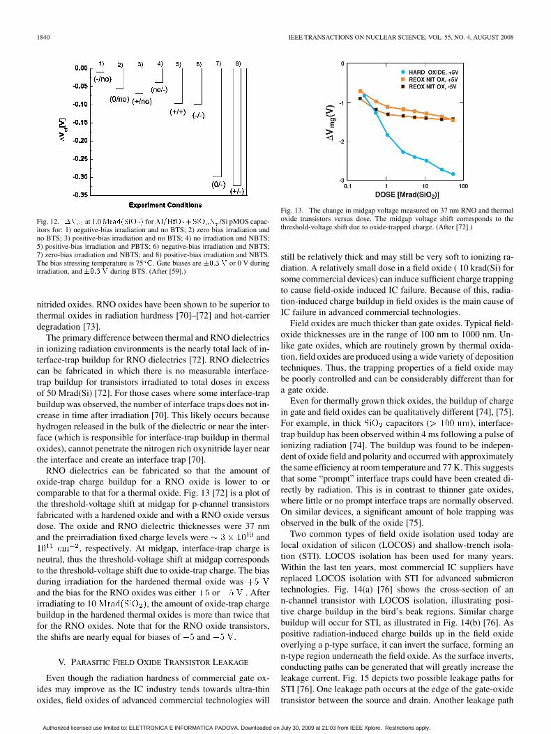
Although the radiation hardness of thin EOT gate ox-ides appears to relatively good, recent results have shown thatthe combined effects of irradiation and bias temperature stress(BTS) can lead to enhanced degradation, as illustrated in Fig. 12[59]. The amount of enhanced degradation was found to dependon the irradiation and anneal bias conditions. Worst-case biaswas for pMOS transistors irradiated in their “OFF” states, andannealed in their “ON” states (the zero/minus state in Fig. 12).
Another alternative dielectric that has been explored in muchmore detail is reoxidized nitrided oxides (RNO) [64]–[69].Nitrided oxides have a lower pin-hole density than , canbe grown at high temperatures permitting better uniformityand less compressive stress and fixed charge, and can retardthe diffusion of dopants through the insulator which can affectthe channel resistivity [65]. These properties make nitridedand RNO dielectrics attractive for ultra-thin gate-oxide com-mercial and hardened devices [65]. Indeed, most advancedcommercial CMOS technologies in production today employ
Authorized licensed use limited to: ELETTRONICA E INFORMATICA PADOVA. Downloaded on July 30, 2009 at 21:03 from IEEE Xplore. Restrictions apply.
1840 IEEE TRANSACTIONS ON NUCLEAR SCIENCE, VOL. 55, NO. 4, AUGUST 2008
Fig. 12. �V at 1.0Mrad(SiO ) forAl=HfO +SiO N /Si pMOS capac-itors for: 1) negative-bias irradiation and no BTS; 2) zero bias irradiation andno BTS; 3) positive-bias irradiation and no BTS; 4) no irradiation and NBTS;5) positive-bias irradiation and PBTS; 6) negative-bias irradiation and NBTS;7) zero-bias irradiation and NBTS; and 8) positive-bias irradiation and NBTS.The bias stressing temperature is 75 C. Gate biases are �0:3 V or 0 V duringirradiation, and �0:3 V during BTS. (After [59].)
nitrided oxides. RNO oxides have been shown to be superior tothermal oxides in radiation hardness [70]–[72] and hot-carrierdegradation [73].
The primary difference between thermal and RNO dielectricsin ionizing radiation environments is the nearly total lack of in-terface-trap buildup for RNO dielectrics [72]. RNO dielectricscan be fabricated in which there is no measurable interface-trap buildup for transistors irradiated to total doses in excessof 50 Mrad(Si) [72]. For those cases where some interface-trapbuildup was observed, the number of interface traps does not in-crease in time after irradiation [70]. This likely occurs becausehydrogen released in the bulk of the dielectric or near the inter-face (which is responsible for interface-trap buildup in thermaloxides), cannot penetrate the nitrogen rich oxynitride layer nearthe interface and create an interface trap [70].
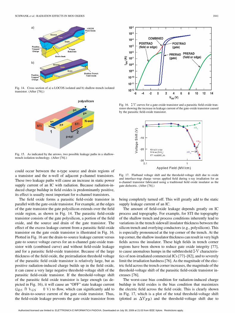
RNO dielectrics can be fabricated so that the amount ofoxide-trap charge buildup for a RNO oxide is lower to orcomparable to that for a thermal oxide. Fig. 13 [72] is a plot ofthe threshold-voltage shift at midgap for p-channel transistorsfabricated with a hardened oxide and with a RNO oxide versusdose. The oxide and RNO dielectric thicknesses were 37 nmand the preirradiation fixed charge levels were and
, respectively. At midgap, interface-trap charge isneutral, thus the threshold-voltage shift at midgap correspondsto the threshold-voltage shift due to oxide-trap charge. The biasduring irradiation for the hardened thermal oxide wasand the bias for the RNO oxides was either or . Afterirradiating to 10 , the amount of oxide-trap chargebuildup in the hardened thermal oxides is more than twice thatfor the RNO oxides. Note that for the RNO oxide transistors,the shifts are nearly equal for biases of and .
V. PARASITIC FIELD OXIDE TRANSISTOR LEAKAGE
Even though the radiation hardness of commercial gate ox-ides may improve as the IC industry tends towards ultra-thinoxides, field oxides of advanced commercial technologies will
Fig. 13. The change in midgap voltage measured on 37 nm RNO and thermaloxide transistors versus dose. The midgap voltage shift corresponds to thethreshold-voltage shift due to oxide-trapped charge. (After [72].)
still be relatively thick and may still be very soft to ionizing ra-diation. A relatively small dose in a field oxide ( 10 krad(Si) forsome commercial devices) can induce sufficient charge trappingto cause field-oxide induced IC failure. Because of this, radia-tion-induced charge buildup in field oxides is the main cause ofIC failure in advanced commercial technologies.
Field oxides are much thicker than gate oxides. Typical field-oxide thicknesses are in the range of 100 nm to 1000 nm. Un-like gate oxides, which are routinely grown by thermal oxida-tion, field oxides are produced using a wide variety of depositiontechniques. Thus, the trapping properties of a field oxide maybe poorly controlled and can be considerably different than fora gate oxide.
Even for thermally grown thick oxides, the buildup of chargein gate and field oxides can be qualitatively different [74], [75].For example, in thick capacitors ( ), interface-trap buildup has been observed within 4 ms following a pulse ofionizing radiation [74]. The buildup was found to be indepen-dent of oxide field and polarity and occurred with approximatelythe same efficiency at room temperature and 77 K. This suggeststhat some “prompt” interface traps could have been created di-rectly by radiation. This is in contrast to thinner gate oxides,where little or no prompt interface traps are normally observed.On similar devices, a significant amount of hole trapping wasobserved in the bulk of the oxide [75].
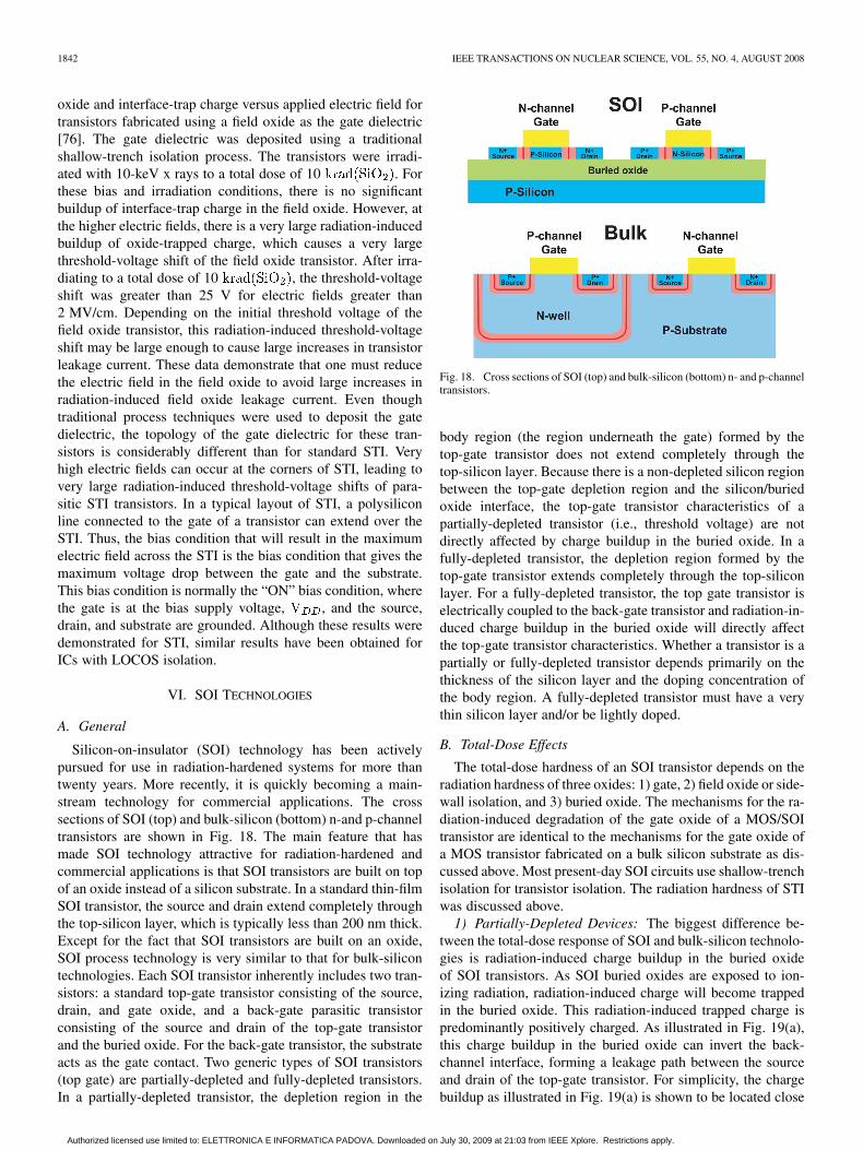
Two common types of field oxide isolation used today arelocal oxidation of silicon (LOCOS) and shallow-trench isola-tion (STI). LOCOS isolation has been used for many years.Within the last ten years, most commercial IC suppliers havereplaced LOCOS isolation with STI for advanced submicrontechnologies. Fig. 14(a) [76] shows the cross-section of ann-channel transistor with LOCOS isolation, illustrating posi-tive charge buildup in the bird’s beak regions. Similar chargebuildup will occur for STI, as illustrated in Fig. 14(b) [76]. Aspositive radiation-induced charge builds up in the field oxideoverlying a p-type surface, it can invert the surface, forming ann-type region underneath the field oxide. As the surface inverts,conducting paths can be generated that will greatly increase theleakage current. Fig. 15 depicts two possible leakage paths forSTI [76]. One leakage path occurs at the edge of the gate-oxidetransistor between the source and drain. Another leakage path
Authorized licensed use limited to: ELETTRONICA E INFORMATICA PADOVA. Downloaded on July 30, 2009 at 21:03 from IEEE Xplore. Restrictions apply.
SCHWANK et al.: RADIATION EFFECTS IN MOS OXIDES 1841
Fig. 14. Cross section of a) a LOCOS isolated and b) shallow-trench isolatedtransistor. (After [76].)
Fig. 15. As indicated by the arrows, two possible leakage paths in a shallow-trench isolation technology. (After [76].)
could occur between the n-type source and drain regions ofa transistor and the n-well of adjacent p-channel transistors.These two leakage paths will cause an increase in static powersupply current of an IC with radiation. Because radiation-in-duced charge buildup in field oxides is predominantly positive,its effect is usually most important for n-channel transistors.
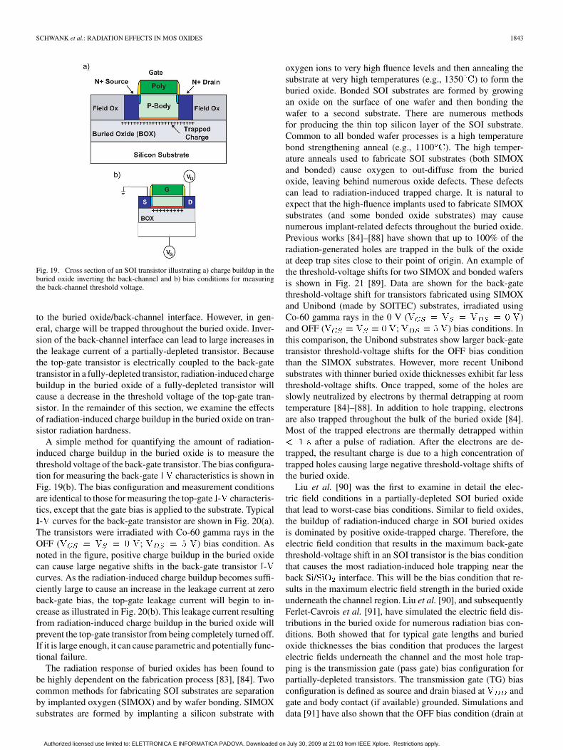
The field oxide forms a parasitic field-oxide transistor inparallel with the gate-oxide transistor. For example, at the edgesof the gate transistor the gate polysilicon extends over the fieldoxide region, as shown in Fig. 14. The parasitic field-oxidetransistor consists of the gate polysilicon, a portion of the fieldoxide, and the source and drain of the gate transistor. Theeffect of the excess leakage current from a parasitic field oxidetransistor on the gate oxide transistor is illustrated in Fig. 16.Plotted in Fig. 16 are the drain-to-source leakage current versusgate-to source voltage curves for an n-channel gate-oxide tran-sistor with (combined curve) and without field-oxide leakageand for a parasitic field-oxide transistor. Because of the largethickness of the field oxide, the preirradiation threshold voltageof the parasitic field oxide transistor is relatively large, but aspositive radiation-induced charge builds up in the field oxide,it can cause a very large negative threshold-voltage shift of theparasitic field-oxide transistor. If the threshold-voltage shiftof the parasitic field oxide transistor is large enough (as de-picted in Fig. 16), it will cause an “OFF” state leakage current( ) to flow, which can significantly add tothe drain-to-source current of the gate oxide transistor. Thus,the field-oxide leakage prevents the gate oxide transistor from
Fig. 16. I-V curves for a gate-oxide transistor and a parasitic field-oxide tran-sistor showing the increase in leakage current of the gate-oxide transistor causedby the parasitic field-oxide transistor.
Fig. 17. Flatband voltage shift and the threshold-voltage shift due to oxideand interface-trap charge versus applied field during x-ray irradiation for ann-channel transistor fabricated using a traditional field oxide insulator as thegate dielectric. (After [76].)
being completely turned off. This will greatly add to the staticsupply leakage current of an IC.
The amount of field-oxide leakage depends greatly on ICprocess and topography. For example, for STI the topographyof the shallow trench and process conditions inherently lead tovariations in the trench sidewall insulator thickness between thesilicon trench and overlying conductors (e.g., polysilicon). Thisis especially pronounced at the top corner of the trench. At thetop corner, the shallow insulator thickness can result in very highfields across the insulator. These high fields in trench cornerregions have been shown to reduce gate oxide integrity [77],to cause anomalous humps in the subthreshold - characteris-tics of non-irradiated commercial ICs [77]–[82], and to severelylimit the irradiation hardness [76]. As the magnitude of the elec-tric field across the trench corner increases, the magnitude of thethreshold-voltage shift of the parasitic field-oxide transistor in-creases [76].
The worst-case bias condition for radiation-induced chargebuildup in field oxides is the bias condition that maximizesthe electric field across the field oxide. This is clearly shownin Fig. 17, which is a plot of the total threshold-voltage shift(plotted as ) and the threshold-voltage shift due to
Authorized licensed use limited to: ELETTRONICA E INFORMATICA PADOVA. Downloaded on July 30, 2009 at 21:03 from IEEE Xplore. Restrictions apply.
1842 IEEE TRANSACTIONS ON NUCLEAR SCIENCE, VOL. 55, NO. 4, AUGUST 2008
oxide and interface-trap charge versus applied electric field fortransistors fabricated using a field oxide as the gate dielectric[76]. The gate dielectric was deposited using a traditionalshallow-trench isolation process. The transistors were irradi-ated with 10-keV x rays to a total dose of 10 . Forthese bias and irradiation conditions, there is no significantbuildup of interface-trap charge in the field oxide. However, atthe higher electric fields, there is a very large radiation-inducedbuildup of oxide-trapped charge, which causes a very largethreshold-voltage shift of the field oxide transistor. After irra-diating to a total dose of 10 , the threshold-voltageshift was greater than 25 V for electric fields greater than2 MV/cm. Depending on the initial threshold voltage of thefield oxide transistor, this radiation-induced threshold-voltageshift may be large enough to cause large increases in transistorleakage current. These data demonstrate that one must reducethe electric field in the field oxide to avoid large increases inradiation-induced field oxide leakage current. Even thoughtraditional process techniques were used to deposit the gatedielectric, the topology of the gate dielectric for these tran-sistors is considerably different than for standard STI. Veryhigh electric fields can occur at the corners of STI, leading tovery large radiation-induced threshold-voltage shifts of para-sitic STI transistors. In a typical layout of STI, a polysiliconline connected to the gate of a transistor can extend over theSTI. Thus, the bias condition that will result in the maximumelectric field across the STI is the bias condition that gives themaximum voltage drop between the gate and the substrate.This bias condition is normally the “ON” bias condition, wherethe gate is at the bias supply voltage, , and the source,drain, and substrate are grounded. Although these results weredemonstrated for STI, similar results have been obtained forICs with LOCOS isolation.
VI. SOI TECHNOLOGIES
A. General
Silicon-on-insulator (SOI) technology has been activelypursued for use in radiation-hardened systems for more thantwenty years. More recently, it is quickly becoming a main-stream technology for commercial applications. The crosssections of SOI (top) and bulk-silicon (bottom) n-and p-channeltransistors are shown in Fig. 18. The main feature that hasmade SOI technology attractive for radiation-hardened andcommercial applications is that SOI transistors are built on topof an oxide instead of a silicon substrate. In a standard thin-filmSOI transistor, the source and drain extend completely throughthe top-silicon layer, which is typically less than 200 nm thick.Except for the fact that SOI transistors are built on an oxide,SOI process technology is very similar to that for bulk-silicontechnologies. Each SOI transistor inherently includes two tran-sistors: a standard top-gate transistor consisting of the source,drain, and gate oxide, and a back-gate parasitic transistorconsisting of the source and drain of the top-gate transistorand the buried oxide. For the back-gate transistor, the substrateacts as the gate contact. Two generic types of SOI transistors(top gate) are partially-depleted and fully-depleted transistors.In a partially-depleted transistor, the depletion region in the
Fig. 18. Cross sections of SOI (top) and bulk-silicon (bottom) n- and p-channeltransistors.
body region (the region underneath the gate) formed by thetop-gate transistor does not extend completely through thetop-silicon layer. Because there is a non-depleted silicon regionbetween the top-gate depletion region and the silicon/buriedoxide interface, the top-gate transistor characteristics of apartially-depleted transistor (i.e., threshold voltage) are notdirectly affected by charge buildup in the buried oxide. In afully-depleted transistor, the depletion region formed by thetop-gate transistor extends completely through the top-siliconlayer. For a fully-depleted transistor, the top gate transistor iselectrically coupled to the back-gate transistor and radiation-in-duced charge buildup in the buried oxide will directly affectthe top-gate transistor characteristics. Whether a transistor is apartially or fully-depleted transistor depends primarily on thethickness of the silicon layer and the doping concentration ofthe body region. A fully-depleted transistor must have a verythin silicon layer and/or be lightly doped.
B. Total-Dose Effects
The total-dose hardness of an SOI transistor depends on theradiation hardness of three oxides: 1) gate, 2) field oxide or side-wall isolation, and 3) buried oxide. The mechanisms for the ra-diation-induced degradation of the gate oxide of a MOS/SOItransistor are identical to the mechanisms for the gate oxide ofa MOS transistor fabricated on a bulk silicon substrate as dis-cussed above. Most present-day SOI circuits use shallow-trenchisolation for transistor isolation. The radiation hardness of STIwas discussed above.
1) Partially-Depleted Devices: The biggest difference be-tween the total-dose response of SOI and bulk-silicon technolo-gies is radiation-induced charge buildup in the buried oxideof SOI transistors. As SOI buried oxides are exposed to ion-izing radiation, radiation-induced charge will become trappedin the buried oxide. This radiation-induced trapped charge ispredominantly positively charged. As illustrated in Fig. 19(a),this charge buildup in the buried oxide can invert the back-channel interface, forming a leakage path between the sourceand drain of the top-gate transistor. For simplicity, the chargebuildup as illustrated in Fig. 19(a) is shown to be located close
Authorized licensed use limited to: ELETTRONICA E INFORMATICA PADOVA. Downloaded on July 30, 2009 at 21:03 from IEEE Xplore. Restrictions apply.
SCHWANK et al.: RADIATION EFFECTS IN MOS OXIDES 1843
Fig. 19. Cross section of an SOI transistor illustrating a) charge buildup in theburied oxide inverting the back-channel and b) bias conditions for measuringthe back-channel threshold voltage.
to the buried oxide/back-channel interface. However, in gen-eral, charge will be trapped throughout the buried oxide. Inver-sion of the back-channel interface can lead to large increases inthe leakage current of a partially-depleted transistor. Becausethe top-gate transistor is electrically coupled to the back-gatetransistor in a fully-depleted transistor, radiation-induced chargebuildup in the buried oxide of a fully-depleted transistor willcause a decrease in the threshold voltage of the top-gate tran-sistor. In the remainder of this section, we examine the effectsof radiation-induced charge buildup in the buried oxide on tran-sistor radiation hardness.
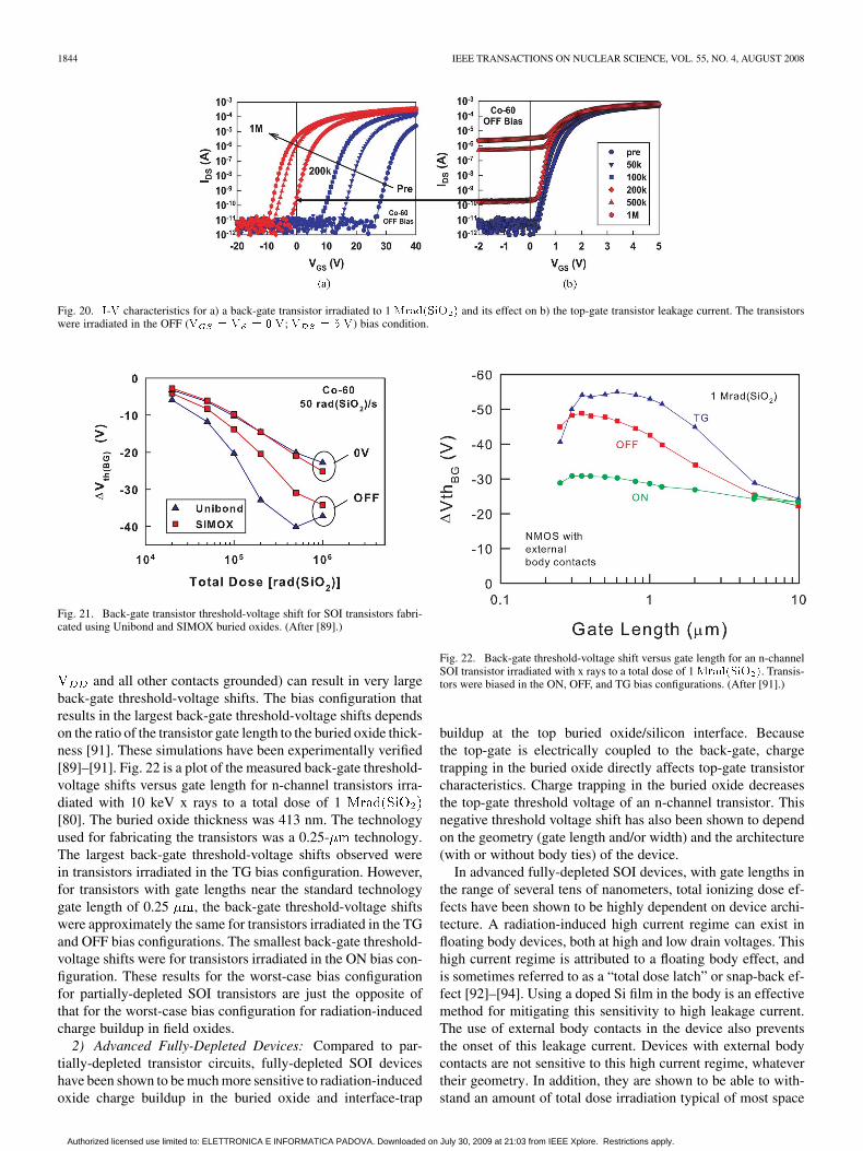
A simple method for quantifying the amount of radiation-induced charge buildup in the buried oxide is to measure thethreshold voltage of the back-gate transistor. The bias configura-tion for measuring the back-gate characteristics is shown inFig. 19(b). The bias configuration and measurement conditionsare identical to those for measuring the top-gate - characteris-tics, except that the gate bias is applied to the substrate. Typical- curves for the back-gate transistor are shown in Fig. 20(a).
The transistors were irradiated with Co-60 gamma rays in theOFF ( ; ) bias condition. Asnoted in the figure, positive charge buildup in the buried oxidecan cause large negative shifts in the back-gate transistor -curves. As the radiation-induced charge buildup becomes suffi-ciently large to cause an increase in the leakage current at zeroback-gate bias, the top-gate leakage current will begin to in-crease as illustrated in Fig. 20(b). This leakage current resultingfrom radiation-induced charge buildup in the buried oxide willprevent the top-gate transistor from being completely turned off.If it is large enough, it can cause parametric and potentially func-tional failure.
The radiation response of buried oxides has been found tobe highly dependent on the fabrication process [83], [84]. Twocommon methods for fabricating SOI substrates are separationby implanted oxygen (SIMOX) and by wafer bonding. SIMOXsubstrates are formed by implanting a silicon substrate with
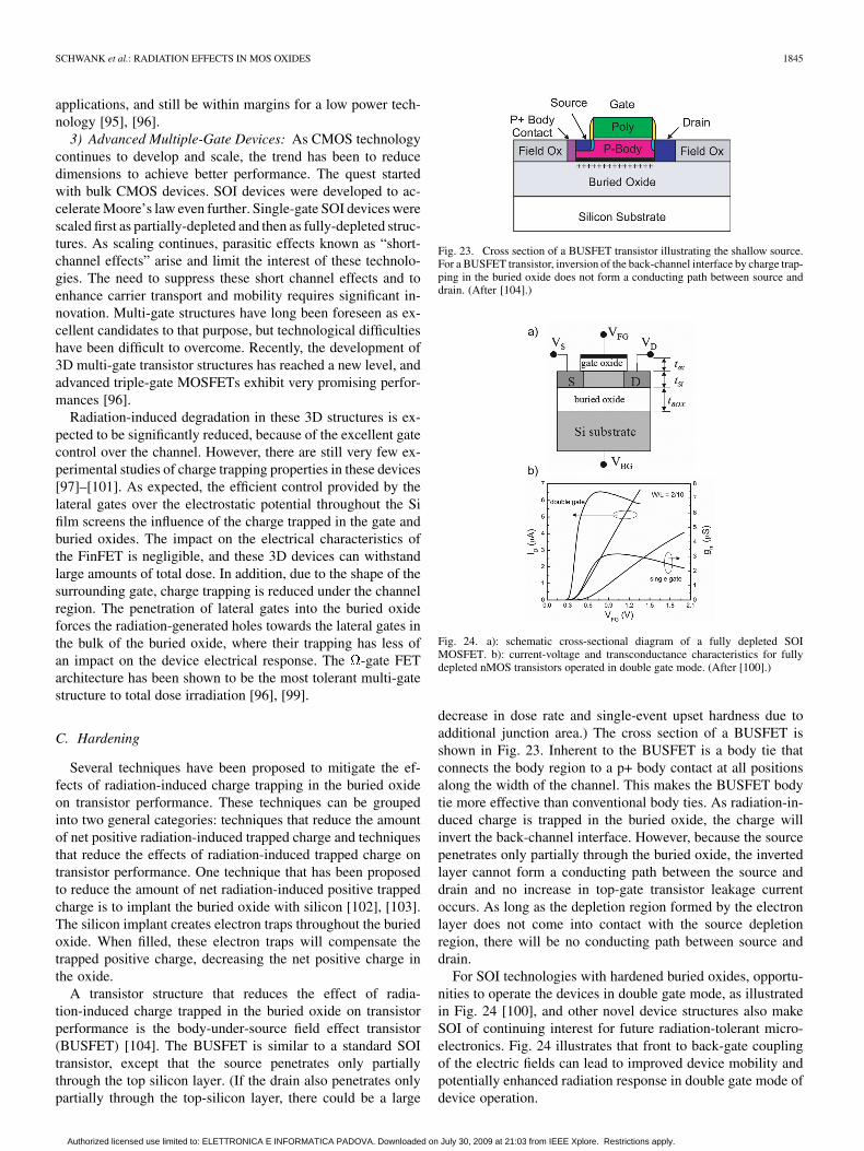
oxygen ions to very high fluence levels and then annealing thesubstrate at very high temperatures (e.g., 1350 ) to form theburied oxide. Bonded SOI substrates are formed by growingan oxide on the surface of one wafer and then bonding thewafer to a second substrate. There are numerous methodsfor producing the thin top silicon layer of the SOI substrate.Common to all bonded wafer processes is a high temperaturebond strengthening anneal (e.g., 1100 ). The high temper-ature anneals used to fabricate SOI substrates (both SIMOXand bonded) cause oxygen to out-diffuse from the buriedoxide, leaving behind numerous oxide defects. These defectscan lead to radiation-induced trapped charge. It is natural toexpect that the high-fluence implants used to fabricate SIMOXsubstrates (and some bonded oxide substrates) may causenumerous implant-related defects throughout the buried oxide.Previous works [84]–[88] have shown that up to 100% of theradiation-generated holes are trapped in the bulk of the oxideat deep trap sites close to their point of origin. An example ofthe threshold-voltage shifts for two SIMOX and bonded wafersis shown in Fig. 21 [89]. Data are shown for the back-gatethreshold-voltage shift for transistors fabricated using SIMOXand Unibond (made by SOITEC) substrates, irradiated usingCo-60 gamma rays in the 0 V ( )and OFF ( ; ) bias conditions. Inthis comparison, the Unibond substrates show larger back-gatetransistor threshold-voltage shifts for the OFF bias conditionthan the SIMOX substrates. However, more recent Unibondsubstrates with thinner buried oxide thicknesses exhibit far lessthreshold-voltage shifts. Once trapped, some of the holes areslowly neutralized by electrons by thermal detrapping at roomtemperature [84]–[88]. In addition to hole trapping, electronsare also trapped throughout the bulk of the buried oxide [84].Most of the trapped electrons are thermally detrapped within
after a pulse of radiation. After the electrons are de-trapped, the resultant charge is due to a high concentration oftrapped holes causing large negative threshold-voltage shifts ofthe buried oxide.
Liu et al. [90] was the first to examine in detail the elec-tric field conditions in a partially-depleted SOI buried oxidethat lead to worst-case bias conditions. Similar to field oxides,the buildup of radiation-induced charge in SOI buried oxidesis dominated by positive oxide-trapped charge. Therefore, theelectric field condition that results in the maximum back-gatethreshold-voltage shift in an SOI transistor is the bias conditionthat causes the most radiation-induced hole trapping near theback Si/ interface. This will be the bias condition that re-sults in the maximum electric field strength in the buried oxideunderneath the channel region. Liu et al. [90], and subsequentlyFerlet-Cavrois et al. [91], have simulated the electric field dis-tributions in the buried oxide for numerous radiation bias con-ditions. Both showed that for typical gate lengths and buriedoxide thicknesses the bias condition that produces the largestelectric fields underneath the channel and the most hole trap-ping is the transmission gate (pass gate) bias configuration forpartially-depleted transistors. The transmission gate (TG) biasconfiguration is defined as source and drain biased at andgate and body contact (if available) grounded. Simulations anddata [91] have also shown that the OFF bias condition (drain at
Authorized licensed use limited to: ELETTRONICA E INFORMATICA PADOVA. Downloaded on July 30, 2009 at 21:03 from IEEE Xplore. Restrictions apply.
1844 IEEE TRANSACTIONS ON NUCLEAR SCIENCE, VOL. 55, NO. 4, AUGUST 2008
Fig. 20. I-V characteristics for a) a back-gate transistor irradiated to 1 Mrad(SiO ) and its effect on b) the top-gate transistor leakage current. The transistorswere irradiated in the OFF (V = V = 0 V; V = 5 V) bias condition.
Fig. 21. Back-gate transistor threshold-voltage shift for SOI transistors fabri-cated using Unibond and SIMOX buried oxides. (After [89].)
and all other contacts grounded) can result in very largeback-gate threshold-voltage shifts. The bias configuration thatresults in the largest back-gate threshold-voltage shifts dependson the ratio of the transistor gate length to the buried oxide thick-ness [91]. These simulations have been experimentally verified[89]–[91]. Fig. 22 is a plot of the measured back-gate threshold-voltage shifts versus gate length for n-channel transistors irra-diated with 10 keV x rays to a total dose of 1[80]. The buried oxide thickness was 413 nm. The technologyused for fabricating the transistors was a 0.25- technology.The largest back-gate threshold-voltage shifts observed werein transistors irradiated in the TG bias configuration. However,for transistors with gate lengths near the standard technologygate length of 0.25 , the back-gate threshold-voltage shiftswere approximately the same for transistors irradiated in the TGand OFF bias configurations. The smallest back-gate threshold-voltage shifts were for transistors irradiated in the ON bias con-figuration. These results for the worst-case bias configurationfor partially-depleted SOI transistors are just the opposite ofthat for the worst-case bias configuration for radiation-inducedcharge buildup in field oxides.
2) Advanced Fully-Depleted Devices: Compared to par-tially-depleted transistor circuits, fully-depleted SOI deviceshave been shown to be much more sensitive to radiation-inducedoxide charge buildup in the buried oxide and interface-trap
Fig. 22. Back-gate threshold-voltage shift versus gate length for an n-channelSOI transistor irradiated with x rays to a total dose of 1 Mrad(SiO ). Transis-tors were biased in the ON, OFF, and TG bias configurations. (After [91].)
buildup at the top buried oxide/silicon interface. Becausethe top-gate is electrically coupled to the back-gate, chargetrapping in the buried oxide directly affects top-gate transistorcharacteristics. Charge trapping in the buried oxide decreasesthe top-gate threshold voltage of an n-channel transistor. Thisnegative threshold voltage shift has also been shown to dependon the geometry (gate length and/or width) and the architecture(with or without body ties) of the device.
In advanced fully-depleted SOI devices, with gate lengths inthe range of several tens of nanometers, total ionizing dose ef-fects have been shown to be highly dependent on device archi-tecture. A radiation-induced high current regime can exist infloating body devices, both at high and low drain voltages. Thishigh current regime is attributed to a floating body effect, andis sometimes referred to as a “total dose latch” or snap-back ef-fect [92]–[94]. Using a doped Si film in the body is an effectivemethod for mitigating this sensitivity to high leakage current.The use of external body contacts in the device also preventsthe onset of this leakage current. Devices with external bodycontacts are not sensitive to this high current regime, whatevertheir geometry. In addition, they are shown to be able to with-stand an amount of total dose irradiation typical of most space
Authorized licensed use limited to: ELETTRONICA E INFORMATICA PADOVA. Downloaded on July 30, 2009 at 21:03 from IEEE Xplore. Restrictions apply.
SCHWANK et al.: RADIATION EFFECTS IN MOS OXIDES 1845
applications, and still be within margins for a low power tech-nology [95], [96].
3) Advanced Multiple-Gate Devices: As CMOS technologycontinues to develop and scale, the trend has been to reducedimensions to achieve better performance. The quest startedwith bulk CMOS devices. SOI devices were developed to ac-celerate Moore’s law even further. Single-gate SOI devices werescaled first as partially-depleted and then as fully-depleted struc-tures. As scaling continues, parasitic effects known as “short-channel effects” arise and limit the interest of these technolo-gies. The need to suppress these short channel effects and toenhance carrier transport and mobility requires significant in-novation. Multi-gate structures have long been foreseen as ex-cellent candidates to that purpose, but technological difficultieshave been difficult to overcome. Recently, the development of3D multi-gate transistor structures has reached a new level, andadvanced triple-gate MOSFETs exhibit very promising perfor-mances [96].
Radiation-induced degradation in these 3D structures is ex-pected to be significantly reduced, because of the excellent gatecontrol over the channel. However, there are still very few ex-perimental studies of charge trapping properties in these devices[97]–[101]. As expected, the efficient control provided by thelateral gates over the electrostatic potential throughout the Sifilm screens the influence of the charge trapped in the gate andburied oxides. The impact on the electrical characteristics ofthe FinFET is negligible, and these 3D devices can withstandlarge amounts of total dose. In addition, due to the shape of thesurrounding gate, charge trapping is reduced under the channelregion. The penetration of lateral gates into the buried oxideforces the radiation-generated holes towards the lateral gates inthe bulk of the buried oxide, where their trapping has less ofan impact on the device electrical response. The -gate FETarchitecture has been shown to be the most tolerant multi-gatestructure to total dose irradiation [96], [99].
C. Hardening
Several techniques have been proposed to mitigate the ef-fects of radiation-induced charge trapping in the buried oxideon transistor performance. These techniques can be groupedinto two general categories: techniques that reduce the amountof net positive radiation-induced trapped charge and techniquesthat reduce the effects of radiation-induced trapped charge ontransistor performance. One technique that has been proposedto reduce the amount of net radiation-induced positive trappedcharge is to implant the buried oxide with silicon [102], [103].The silicon implant creates electron traps throughout the buriedoxide. When filled, these electron traps will compensate thetrapped positive charge, decreasing the net positive charge inthe oxide.
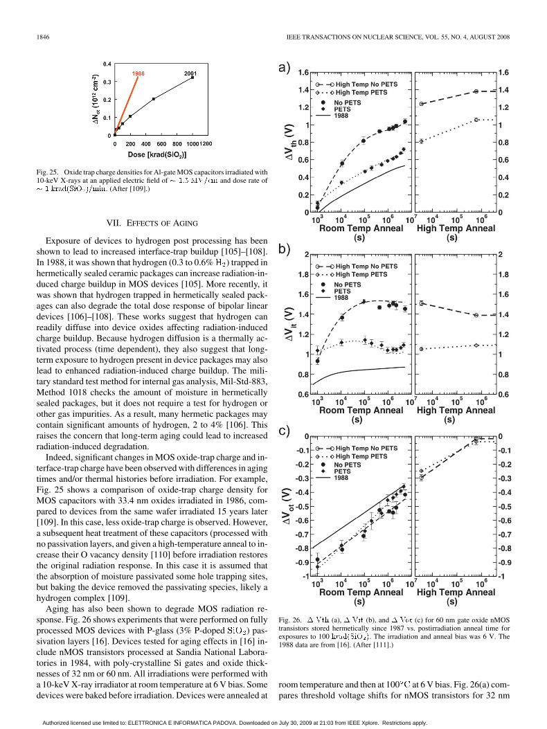
A transistor structure that reduces the effect of radia-tion-induced charge trapped in the buried oxide on transistorperformance is the body-under-source field effect transistor(BUSFET) [104]. The BUSFET is similar to a standard SOItransistor, except that the source penetrates only partiallythrough the top silicon layer. (If the drain also penetrates onlypartially through the top-silicon layer, there could be a large
Fig. 23. Cross section of a BUSFET transistor illustrating the shallow source.For a BUSFET transistor, inversion of the back-channel interface by charge trap-ping in the buried oxide does not form a conducting path between source anddrain. (After [104].)
Fig. 24. a): schematic cross-sectional diagram of a fully depleted SOIMOSFET. b): current-voltage and transconductance characteristics for fullydepleted nMOS transistors operated in double gate mode. (After [100].)
decrease in dose rate and single-event upset hardness due toadditional junction area.) The cross section of a BUSFET isshown in Fig. 23. Inherent to the BUSFET is a body tie thatconnects the body region to a p+ body contact at all positionsalong the width of the channel. This makes the BUSFET bodytie more effective than conventional body ties. As radiation-in-duced charge is trapped in the buried oxide, the charge willinvert the back-channel interface. However, because the sourcepenetrates only partially through the buried oxide, the invertedlayer cannot form a conducting path between the source anddrain and no increase in top-gate transistor leakage currentoccurs. As long as the depletion region formed by the electronlayer does not come into contact with the source depletionregion, there will be no conducting path between source anddrain.
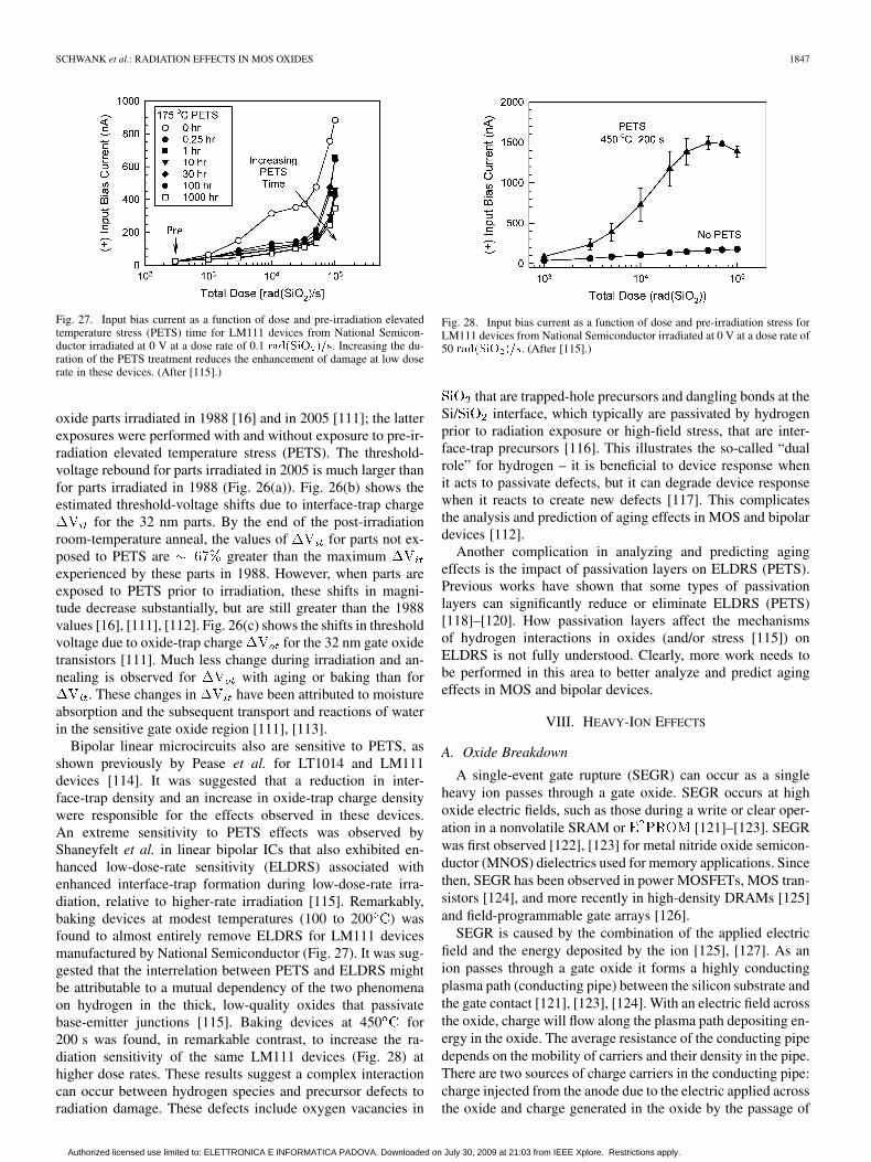
For SOI technologies with hardened buried oxides, opportu-nities to operate the devices in double gate mode, as illustratedin Fig. 24 [100], and other novel device structures also makeSOI of continuing interest for future radiation-tolerant micro-electronics. Fig. 24 illustrates that front to back-gate couplingof the electric fields can lead to improved device mobility andpotentially enhanced radiation response in double gate mode ofdevice operation.
Authorized licensed use limited to: ELETTRONICA E INFORMATICA PADOVA. Downloaded on July 30, 2009 at 21:03 from IEEE Xplore. Restrictions apply.
1846 IEEE TRANSACTIONS ON NUCLEAR SCIENCE, VOL. 55, NO. 4, AUGUST 2008
Fig. 25. Oxide trap charge densities for Al-gate MOS capacitors irradiated with10-keV X-rays at an applied electric field of � 1:5 MV=cm and dose rate of� 1 krad(SiO )=min. (After [109].)
VII. EFFECTS OF AGING
Exposure of devices to hydrogen post processing has beenshown to lead to increased interface-trap buildup [105]–[108].In 1988, it was shown that hydrogen (0.3 to 0.6% ) trapped inhermetically sealed ceramic packages can increase radiation-in-duced charge buildup in MOS devices [105]. More recently, itwas shown that hydrogen trapped in hermetically sealed pack-ages can also degrade the total dose response of bipolar lineardevices [106]–[108]. These works suggest that hydrogen canreadily diffuse into device oxides affecting radiation-inducedcharge buildup. Because hydrogen diffusion is a thermally ac-tivated process (time dependent), they also suggest that long-term exposure to hydrogen present in device packages may alsolead to enhanced radiation-induced charge buildup. The mili-tary standard test method for internal gas analysis, Mil-Std-883,Method 1018 checks the amount of moisture in hermeticallysealed packages, but it does not require a test for hydrogen orother gas impurities. As a result, many hermetic packages maycontain significant amounts of hydrogen, 2 to 4% [106]. Thisraises the concern that long-term aging could lead to increasedradiation-induced degradation.
Indeed, significant changes in MOS oxide-trap charge and in-terface-trap charge have been observed with differences in agingtimes and/or thermal histories before irradiation. For example,Fig. 25 shows a comparison of oxide-trap charge density forMOS capacitors with 33.4 nm oxides irradiated in 1986, com-pared to devices from the same wafer irradiated 15 years later[109]. In this case, less oxide-trap charge is observed. However,a subsequent heat treatment of these capacitors (processed withno passivation layers, and given a high-temperature anneal to in-crease their O vacancy density [110] before irradiation restoresthe original radiation response. In this case it is assumed thatthe absorption of moisture passivated some hole trapping sites,but baking the device removed the passivating species, likely ahydrogen complex [109].
Aging has also been shown to degrade MOS radiation re-sponse. Fig. 26 shows experiments that were performed on fullyprocessed MOS devices with P-glass (3% P-doped ) pas-sivation layers [16]. Devices tested for aging effects in [16] in-clude nMOS transistors processed at Sandia National Labora-tories in 1984, with poly-crystalline Si gates and oxide thick-nesses of 32 nm or 60 nm. All irradiations were performed witha 10-keV X-ray irradiator at room temperature at 6 V bias. Somedevices were baked before irradiation. Devices were annealed at
Fig. 26. � Vth (a), � Vit (b), and � Vot (c) for 60 nm gate oxide nMOStransistors stored hermetically since 1987 vs. postirradiation anneal time forexposures to 100 krad(SiO ). The irradiation and anneal bias was 6 V. The1988 data are from [16]. (After [111].)
room temperature and then at 100 at 6 V bias. Fig. 26(a) com-pares threshold voltage shifts for nMOS transistors for 32 nm
Authorized licensed use limited to: ELETTRONICA E INFORMATICA PADOVA. Downloaded on July 30, 2009 at 21:03 from IEEE Xplore. Restrictions apply.
SCHWANK et al.: RADIATION EFFECTS IN MOS OXIDES 1847
Fig. 27. Input bias current as a function of dose and pre-irradiation elevatedtemperature stress (PETS) time for LM111 devices from National Semicon-ductor irradiated at 0 V at a dose rate of 0.1 rad(SiO )=s. Increasing the du-ration of the PETS treatment reduces the enhancement of damage at low doserate in these devices. (After [115].)
oxide parts irradiated in 1988 [16] and in 2005 [111]; the latterexposures were performed with and without exposure to pre-ir-radiation elevated temperature stress (PETS). The threshold-voltage rebound for parts irradiated in 2005 is much larger thanfor parts irradiated in 1988 (Fig. 26(a)). Fig. 26(b) shows theestimated threshold-voltage shifts due to interface-trap charge
for the 32 nm parts. By the end of the post-irradiationroom-temperature anneal, the values of for parts not ex-posed to PETS are greater than the maximumexperienced by these parts in 1988. However, when parts areexposed to PETS prior to irradiation, these shifts in magni-tude decrease substantially, but are still greater than the 1988values [16], [111], [112]. Fig. 26(c) shows the shifts in thresholdvoltage due to oxide-trap charge for the 32 nm gate oxidetransistors [111]. Much less change during irradiation and an-nealing is observed for with aging or baking than for
. These changes in have been attributed to moistureabsorption and the subsequent transport and reactions of waterin the sensitive gate oxide region [111], [113].
Bipolar linear microcircuits also are sensitive to PETS, asshown previously by Pease et al. for LT1014 and LM111devices [114]. It was suggested that a reduction in inter-face-trap density and an increase in oxide-trap charge densitywere responsible for the effects observed in these devices.An extreme sensitivity to PETS effects was observed byShaneyfelt et al. in linear bipolar ICs that also exhibited en-hanced low-dose-rate sensitivity (ELDRS) associated withenhanced interface-trap formation during low-dose-rate irra-diation, relative to higher-rate irradiation [115]. Remarkably,baking devices at modest temperatures (100 to 200 ) wasfound to almost entirely remove ELDRS for LM111 devicesmanufactured by National Semiconductor (Fig. 27). It was sug-gested that the interrelation between PETS and ELDRS mightbe attributable to a mutual dependency of the two phenomenaon hydrogen in the thick, low-quality oxides that passivatebase-emitter junctions [115]. Baking devices at 450 for200 s was found, in remarkable contrast, to increase the ra-diation sensitivity of the same LM111 devices (Fig. 28) athigher dose rates. These results suggest a complex interactioncan occur between hydrogen species and precursor defects toradiation damage. These defects include oxygen vacancies in
Fig. 28. Input bias current as a function of dose and pre-irradiation stress forLM111 devices from National Semiconductor irradiated at 0 V at a dose rate of50 rad(SiO )=s. (After [115].)
that are trapped-hole precursors and dangling bonds at theSi/ interface, which typically are passivated by hydrogenprior to radiation exposure or high-field stress, that are inter-face-trap precursors [116]. This illustrates the so-called “dualrole” for hydrogen – it is beneficial to device response whenit acts to passivate defects, but it can degrade device responsewhen it reacts to create new defects [117]. This complicatesthe analysis and prediction of aging effects in MOS and bipolardevices [112].
Another complication in analyzing and predicting agingeffects is the impact of passivation layers on ELDRS (PETS).Previous works have shown that some types of passivationlayers can significantly reduce or eliminate ELDRS (PETS)[118]–[120]. How passivation layers affect the mechanismsof hydrogen interactions in oxides (and/or stress [115]) onELDRS is not fully understood. Clearly, more work needs tobe performed in this area to better analyze and predict agingeffects in MOS and bipolar devices.
VIII. HEAVY-ION EFFECTS
A. Oxide Breakdown
A single-event gate rupture (SEGR) can occur as a singleheavy ion passes through a gate oxide. SEGR occurs at highoxide electric fields, such as those during a write or clear oper-ation in a nonvolatile SRAM or [121]–[123]. SEGRwas first observed [122], [123] for metal nitride oxide semicon-ductor (MNOS) dielectrics used for memory applications. Sincethen, SEGR has been observed in power MOSFETs, MOS tran-sistors [124], and more recently in high-density DRAMs [125]and field-programmable gate arrays [126].
SEGR is caused by the combination of the applied electricfield and the energy deposited by the ion [125], [127]. As anion passes through a gate oxide it forms a highly conductingplasma path (conducting pipe) between the silicon substrate andthe gate contact [121], [123], [124]. With an electric field acrossthe oxide, charge will flow along the plasma path depositing en-ergy in the oxide. The average resistance of the conducting pipedepends on the mobility of carriers and their density in the pipe.There are two sources of charge carriers in the conducting pipe:charge injected from the anode due to the electric applied acrossthe oxide and charge generated in the oxide by the passage of
Authorized licensed use limited to: ELETTRONICA E INFORMATICA PADOVA. Downloaded on July 30, 2009 at 21:03 from IEEE Xplore. Restrictions apply.
1848 IEEE TRANSACTIONS ON NUCLEAR SCIENCE, VOL. 55, NO. 4, AUGUST 2008
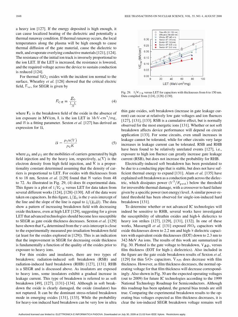
a heavy ion [127]. If the energy deposited is high enough, itcan cause localized heating of the dielectric and potentially athermal runaway condition. If thermal runaway occurs, the localtemperatures along the plasma will be high enough to causethermal diffusion of the gate material, cause the dielectric tomelt, and evaporate overlying conductive materials [121], [124].The resistance of the initial ion track is inversely proportional tothe ion LET. If the LET is increased, the resistance is lowered,and the required voltage across the device to sustain conductionis reduced [124].
For thermal oxides with the incident ion normal to thesurface, Wheatley et al. [128] showed that the critical electricfield, , for SEGR is given by
(4)
where is the breakdown field of the oxide in the absence ofion exposure in MV/cm, is the ion LET in ,and is a fitting parameter. Sexton et al. [127] has derived anexpression for ,
(5)
where and are the mobilities of carriers generated by highfield injection and by the heavy ion, respectively, is theelectron density from high field injection, and is a propor-tionality constant determined assuming that the density of car-riers is proportional to LET. For oxides with thicknesses from6 to 18 nm, Sexton et al. [129] found that varies from 48to 72. As illustrated in Fig. 29, (4) does fit experimental data.This figure is a plot of versus LET for data taken fromseveral different works [124], [128]–[130]. All of the data weretaken on capacitors. In this figure, is the -axis intercept ofthe line and the slope of the line is equal to . The datashow a pattern of increasing breakdown field with decreasingoxide thickness, even at high LET [129], suggesting for a givenLET that advanced technologies should become less susceptibleto SEGR as gate oxide thickness decreases. Sexton et al. [129]have shown that determined from the -axis intercept is closeto the experimentally measured pre-irradiation breakdown field(at least for the oxides explored in [129]). This is an indicationthat the improvement in SEGR for decreasing oxide thicknessis fundamentally a function of the quality of the oxides prior toexposure to heavy ions.
For thin oxides and insulators, there are two types ofbreakdown; radiation-induced soft breakdown (RSB) andradiation-induced hard breakdown (RHB) [127], [131]. RHBis a SEGR and is discussed above. As insulators are exposedto heavy ions, some insulators exhibit a gradual increase inleakage current. This type of breakdown is referred to as softbreakdown [49], [127], [131]–[134]. Although in soft break-down the oxide is clearly damaged, the oxide (insulator) hasnot ruptured. It can be the dominant stress-related breakdownmode in emerging oxides [131], [133]. While the probabilityfor heavy-ion induced hard breakdown can be very low in ultra
Fig. 29. 1=E versus LET for capacitors with thicknesses from 6 to 150 nm.Data compiled from [124], [128]–[130].
thin gate oxides, soft breakdown (increase in gate leakage cur-rent) can occur at relatively low gate voltages and ion fluences[127], [131], [133]. RSB is a cumulative effect, but is normallyobserved for the most energetic ions [131]. Whether or not softbreakdown affects device performance will depend on circuitapplication [133]. For some circuits, even small increases inleakage cannot be tolerated, while for other circuits very largeincreases in leakage current can be tolerated. RSB and RHBhave been found to be relatively unrelated events [127], i.e.,exposure to high ion fluence can greatly increase gate leakagecurrent (RSB), but does not increase the probability for RHB.
Electrically-induced soft breakdown has been postulated tobe due to a conducting pipe that is stable, but does not have suf-ficient thermal energy to expand [131]. Alam et al. [135] haveexplained soft breakdown as a conduction path across the dielec-tric, which dissipates power ( ) below the thresholdfor irreversible thermal damage, with a crossover to hard failuregiven by a specific power (not energy) level. A similar power-re-lated threshold has been observed for single-ion-induced hardbreakdown [131].
To determine whether or not advanced IC technologies willindeed be sensitive to RHB, several works have investigatedthe susceptibility of ultrathin oxides and high- dielecrics toheavy ion strikes [127], [129], [131], [132]. In one of theseworks, Massengill et al. [131] exposed capacitors withoxide thicknesses down to 2.2 nm and high- dielectric capaci-tors with equivalent oxide thicknesses (EOT) down to 2.3 nm to342-MeV Au ions. The results of this work are summarized inFig. 30. Plotted is the gate voltage to breakdown, , versusfilm thickness (EOT for high- dielectrics). Also included inthe figure are the gate oxide breakdown results of Sexton et al.[129] for thin capacitors. does decrease with filmthickness. However, as film thickness decreases, the normal op-erating voltage for that film thickness will decrease correspond-ingly. Also shown in Fig. 30 are the expected operating voltages(out to 2009) for future IC technologies according to the 1999National Technology Roadmap for Semiconductors. Althoughthis roadmap has been updated, the general bias trends are stilltrue. Comparing the experimental breakdown results to the op-erating bias voltages expected as film thickness decreases, it isclear the ion-induced SEGR breakdown voltage remains well
Authorized licensed use limited to: ELETTRONICA E INFORMATICA PADOVA. Downloaded on July 30, 2009 at 21:03 from IEEE Xplore. Restrictions apply.
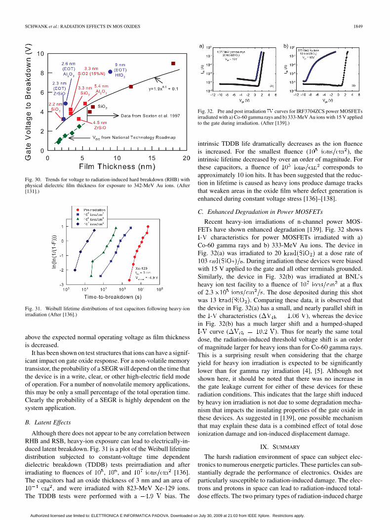
SCHWANK et al.: RADIATION EFFECTS IN MOS OXIDES 1849
Fig. 30. Trends for voltage to radiation-induced hard breakdown (RHB) withphysical dielectric film thickness for exposure to 342-MeV Au ions. (After[131].)
Fig. 31. Weibull lifetime distributions of test capacitors following heavy-ionirradiation (After [136].)
above the expected normal operating voltage as film thicknessis decreased.
It has been shown on test structures that ions can have a signif-icant impact on gate oxide response. For a non-volatile memorytransistor, the probability of a SEGR will depend on the time thatthe device is in a write, clear, or other high-electric field modeof operation. For a number of nonvolatile memory applications,this may be only a small percentage of the total operation time.Clearly the probability of a SEGR is highly dependent on thesystem application.
B. Latent Effects
Although there does not appear to be any correlation betweenRHB and RSB, heavy-ion exposure can lead to electrically-in-duced latent breakdown. Fig. 31 is a plot of the Weibull lifetimedistribution subjected to constant-voltage time dependentdielectric breakdown (TDDB) tests preirradiation and afterirradiating to fluences of , , and [136].The capacitors had an oxide thickness of 3 nm and an area of
, and were irradiated with 823-MeV Xe-129 ions.The TDDB tests were performed with a bias. The
Fig. 32. Pre and post irradiation IV curves for IRF3704ZCS power MOSFETsirradiated with a) Co-60 gamma rays and b) 333-MeV Au ions with 15 V appliedto the gate during irradiation. (After [139].)
intrinsic TDDB life dramatically decreases as the ion fluenceis increased. For the smallest fluence ( ), theintrinsic lifetime decreased by over an order of magnitude. Forthese capacitors, a fluence of corresponds toapproximately 10 ion hits. It has been suggested that the reduc-tion in lifetime is caused as heavy ions produce damage tracksthat weaken areas in the oxide film where defect generation isenhanced during constant voltage stress [136]–[138].
C. Enhanced Degradation in Power MOSFETs
Recent heavy-ion irradiations of n-channel power MOS-FETs have shown enhanced degradation [139]. Fig. 32 shows- characteristics for power MOSFETs irradiated with a)
Co-60 gamma rays and b) 333-MeV Au ions. The device inFig. 32(a) was irradiated to 20 at a dose rate of103 . During irradiation these devices were biasedwith 15 V applied to the gate and all other terminals grounded.Similarly, the device in Fig. 32(b) was irradiated at BNL’sheavy ion test facility to a fluence of at a fluxof 2.3 . The dose deposited during this shotwas 13 . Comparing these data, it is observed thatthe device in Fig. 32(a) has a small, and nearly parallel shift inthe - characteristics ( ), whereas the devicein Fig. 32(b) has a much larger shift and a humped-shaped- curve ( ). Thus for nearly the same total
dose, the radiation-induced threshold voltage shift is an orderof magnitude larger for heavy ions than for Co-60 gamma rays.This is a surprising result when considering that the chargeyield for heavy ion irradiation is expected to be significantlylower than for gamma ray irradiation [4], [5]. Although notshown here, it should be noted that there was no increase inthe gate leakage current for either of these devices for theseradiation conditions. This indicates that the large shift inducedby heavy ion irradiation is not due to some degradation mecha-nism that impacts the insulating properties of the gate oxide inthese devices. As suggested in [139], one possible mechanismthat may explain these data is a combined effect of total doseionization damage and ion-induced displacement damage.
IX. SUMMARY
The harsh radiation environment of space can subject elec-tronics to numerous energetic particles. These particles can sub-stantially degrade the performance of electronics. Oxides areparticularly susceptible to radiation-induced damage. The elec-trons and protons in space can lead to radiation-induced total-dose effects. The two primary types of radiation-induced charge
Authorized licensed use limited to: ELETTRONICA E INFORMATICA PADOVA. Downloaded on July 30, 2009 at 21:03 from IEEE Xplore. Restrictions apply.
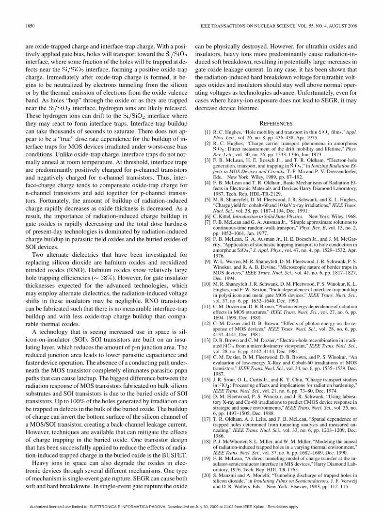
1850 IEEE TRANSACTIONS ON NUCLEAR SCIENCE, VOL. 55, NO. 4, AUGUST 2008
are oxide-trapped charge and interface-trap charge. With a posi-tively applied gate bias, holes will transport toward theinterface, where some fraction of the holes will be trapped at de-fects near the interface, forming a positive oxide-trapcharge. Immediately after oxide-trap charge is formed, it be-gins to be neutralized by electrons tunneling from the siliconor by the thermal emission of electrons from the oxide valenceband. As holes “hop” through the oxide or as they are trappednear the interface, hydrogen ions are likely released.These hydrogen ions can drift to the interface wherethey may react to form interface traps. Interface-trap buildupcan take thousands of seconds to saturate. There does not ap-pear to be a “true” dose rate dependence for the buildup of in-terface traps for MOS devices irradiated under worst-case biasconditions. Unlike oxide-trap charge, interface traps do not nor-mally anneal at room temperature. At threshold, interface trapsare predominantly positively charged for p-channel transistorsand negatively charged for n-channel transistors. Thus, inter-face-charge charge tends to compensate oxide-trap charge forn-channel transistors and add together for p-channel transis-tors. Fortunately, the amount of buildup of radiation-inducedcharge rapidly decreases as oxide thickness is decreased. As aresult, the importance of radiation-induced charge buildup ingate oxides is rapidly decreasing and the total dose hardnessof present-day technologies is dominated by radiation-inducedcharge buildup in parasitic field oxides and the buried oxides ofSOI devices.
Two alternate dielectrics that have been investigated forreplacing silicon dioxide are hafnium oxides and reoxidizednitrided oxides (RNO). Hafnium oxides show relatively largehole trapping efficiencies ( ). However, for gate insulatorthicknesses expected for the advanced technologies, whichmay employ alternate dielectrics, the radiation-induced voltageshifts in these insulators may be negligible. RNO transistorscan be fabricated such that there is no measurable interface-trapbuildup and with less oxide-trap charge buildup than compa-rable thermal oxides.
A technology that is seeing increased use in space is sil-icon-on-insulator (SOI). SOI transistors are built on an insu-lating layer, which reduces the amount of p-n junction area. Thereduced junction area leads to lower parasitic capacitance andfaster device operation. The absence of a conducting path under-neath the MOS transistor completely eliminates parasitic pnpnpaths that can cause latchup. The biggest difference between theradiation response of MOS transistors fabricated on bulk siliconsubstrates and SOI transistors is due to the buried oxide of SOItransistors. Up to 100% of the holes generated by irradiation canbe trapped in defects in the bulk of the buried oxide. The buildupof charge can invert the bottom surface of the silicon channel ofa MOS/SOI transistor, creating a back-channel leakage current.However, techniques are available that can mitigate the effectsof charge trapping in the buried oxide. One transistor designthat has been successfully applied to reduce the effects of radia-tion-induced trapped charge in the buried oxide is the BUSFET.
Heavy ions in space can also degrade the oxides in elec-tronic devices through several different mechanisms. One typeof mechanism is single-event gate rupture. SEGR can cause bothsoft and hard breakdowns. In single-event gate rupture the oxide
can be physically destroyed. However, for ultrathin oxides andinsulators, heavy ions more predominantly cause radiation-in-duced soft breakdown, resulting in potentially large increases ingate oxide leakage current. In any case, it has been shown thatthe radiation-induced hard breakdown voltage for ultrathin volt-ages oxides and insulators should stay well above normal oper-ating voltages as technologies advance. Unfortunately, even forcases where heavy-ion exposure does not lead to SEGR, it maydecrease device lifetime.
REFERENCES
[1] R. C. Hughes, “Hole mobility and transport in thin SiO films,” Appl.Phys. Lett., vol. 26, no. 8, pp. 436–438, Apr. 1975.
[2] R. C. Hughes, “Charge carrier transport phenomena in amorphousSiO : Direct measurement of the drift mobility and lifetime,” Phys.Rev. Lett., vol. 30, no. 26, pp. 1333–1336, Jun. 1973.
[3] F. B. McLean, H. E. Boesch Jr., and T. R. Oldham, “Electron-holegeneration, transport, and trapping in SiO ,” in Ionizing Radiation Ef-fects in MOS Devices and Circuits, T. P. Ma and P. V. Dressendorfer,Eds. New York: Wiley, 1989, pp. 87–192.
[4] F. B. McLean and T. R. Oldham, Basic Mechanisms of Radiation Ef-fects in Electronic Materials and Devices Harry Diamond Laboratory,1987, Tech. Rep. HDL-TR-2129.
[5] M. R. Shaneyfelt, D. M. Fleetwood, J. R. Schwank, and K. L. Hughes,“Charge yield for cobalt-60 and 10 keV x-ray irradiations,” IEEE Trans.Nucl. Sci., vol. 38, pp. 1187–1194, Dec. 1991.
[6] C. Kittel, Introduction to Solid State Physics. New York: Wiley, 1968.[7] F. B. McLean and G. A. Ausman Jr., “Simple approximate solutions to
continuous-time random-walk transport,” Phys. Rev. B, vol. 15, no. 2,pp. 1052–1061, Jan. 1977.
[8] F. B. McLean, G. A. Ausman Jr., H. E. Boesch Jr., and J. M. McGar-rity, “Application of stochastic hopping transport to hole conduction inamorphous SiO ,” J. Appl. Phys., vol. 47, no. 4, pp. 1529–1532, Apr.1976.
[9] W. L. Warren, M. R. Shaneyfelt, D. M. Fleetwood, J. R. Schwank, P. S.Winokur, and R. A. B. Devine, “Microscopic nature of border traps inMOS devices,” IEEE Trans. Nucl. Sci., vol. 41, no. 6, pp. 1817–1827,Dec. 1994.
[10] M. R. Shaneyfelt, J. R. Schwank, D. M. Fleetwood, P. S. Winokur, K. L.Hughes, and F. W. Sexton, “Field dependence of interface trap buildupin polysilicon and metal gate MOS devices,” IEEE Trans. Nucl. Sci.,vol. 37, no. 6, pp. 1632–1640, Dec. 1990.
[11] C. M. Dozier and D. B. Brown, “Photon energy dependence of radiationeffects in MOS structures,” IEEE Trans. Nucl. Sci., vol. 27, no. 6, pp.1694–1699, Dec. 1980.
[12] C. M. Dozier and D. B. Brown, “Effects of photon energy on the re-sponse of MOS devices,” IEEE Trans. Nucl. Sci., vol. 28, no. 6, pp.4137–4141, Dec. 1981.
[13] D. B. Brown and C. M. Dozier, “Electron-hole recombination in irradi-ated SiO from a microdosimetry viewpoint,” IEEE Trans. Nucl. Sci.,vol. 28, no. 6, pp. 4142–4144, Dec. 1981.
[14] C. M. Dozier, D. M. Fleetwood, D. B. Brown, and P. S. Winokur, “Anevaluation of low-energy X-Ray and Cobalt-60 irradiations of MOStransistors,” IEEE Trans. Nucl. Sci., vol. 34, no. 6, pp. 1535–1539, Dec.1987.
[15] J. R. Srour, O. L. Curtis Jr., and K. Y. Chiu, “Charge transport studiesin SiO : Processing effects and implications for radiation hardening,”IEEE Trans. Nucl. Sci., vol. 21, no. 6, pp. 73–80, Dec. 1974.
[16] D. M. Fleetwood, P. S. Winokur, and J. R. Schwank, “Using labora-tory X-ray and Co-60 irradiations to predict CMOS device response instrategic and space environments,” IEEE Trans. Nucl. Sci., vol. 35, no.6, pp. 1497–1505, Dec. 1988.
[17] T. R. Oldham, A. J. Lelis, and F. B. McLean, “Spatial dependence oftrapped holes determined from tunneling analysis and measured an-nealing,” IEEE Trans. Nucl. Sci., vol. 33, no. 6, pp. 1203–1209, Dec.1986.
[18] P. J. McWhorter, S. L. Miller, and W. M. Miller, “Modeling the annealof radiation-induced trapped holes in a varying thermal environment,”IEEE Trans. Nucl. Sci., vol. 37, no. 6, pp. 1682–1689, Dec. 1990.
[19] F. B. McLean, “A direct tunneling model of charge transfer at the in-sulator-semiconductor interface in MIS devices,” Harry Diamond Lab-oratory, 1976, Tech. Rep. HDL-TR-1765.
[20] S. Manzini and A. Modelli, “Tunneling discharge of trapped holes insilicon dioxide,” in Insulating Films on Semiconductors, J. F. Verweijand D. R. Wolters, Eds. New York: Elsevier, 1983, pp. 112–115.
Authorized licensed use limited to: ELETTRONICA E INFORMATICA PADOVA. Downloaded on July 30, 2009 at 21:03 from IEEE Xplore. Restrictions apply.
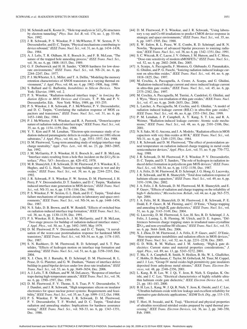
SCHWANK et al.: RADIATION EFFECTS IN MOS OXIDES 1851
[21] M. Schmidt and K. Koster Jr., “Hole trap analysis in SiO /Si structuresby electron tunneling,” Phys. Stat. Sol. B, vol. 174, no. 1, pp. 53–66,Nov. 1992.
[22] J. R. Schwank, P. S. Winokur, P. J. McWhorter, F. W. Sexton, P. V.Dressendorfer, and D. C. Turpin, “Physical mechanisms contributing todevice rebound,” IEEE Trans. Nucl. Sci., vol. 31, no. 6, pp. 1434–1438,Dec. 1984.
[23] A. J. Lelis, T. R. Oldham, H. E. Boesch Jr., and F. B. McLean, “Thenature of the trapped hole annealing process,” IEEE Trans. Nucl. Sci.,vol. 36, no. 6, pp. 1808–1815, Dec. 1989.
[24] G. F. Derbenwick and H. H. Sander, “CMOS hardness for low-dose-rate environments,” IEEE Trans. Nucl. Sci., vol. NS–24, no. 6, pp.2244–2247, Dec. 1977.
[25] P. J. McWhorter, S. L. Miller, and T. A. Dellin, “Modeling the memoryretention characteristics of SNOS transistors in a varying thermal en-vironment,” J. Appl. Phys, vol. 68, no. 4, pp. 1902–1908, Aug. 1990.
[26] S. Ballard and G. Barbottin, Instabilities in Silicon Devices. NewYork: Elsevier, 1989, vol. 2.
[27] P. S. Winokur, “Radiation-induced interface traps,” in Ionizing Ra-diation Effects in MOS Devices and Circuits, T. P. Ma and P. V.Dressendorfer, Eds. New York: Wiley, 1989, pp. 193–255.
[28] P. S. Winokur, J. R. Schwank, P. J. McWhorter, P. V. Dressendorfer,and D. C. Turpin, “Correlating the radiation response of MOS ca-pacitors and transistors,” IEEE Trans. Nucl. Sci., vol. 31, no. 6, pp.1453–1460, Dec. 1984.
[29] P. J. McWhorter, P. S. Winokur, and R. A. Pastorek, “Donor/acceptornature of radiation-induced interface traps,” IEEE Trans. Nucl. Sci., vol.35, no. 6, pp. 1154–1159, Dec. 1988.
[30] Y. Y. Kim and P. M. Lenahan, “Electron-spin resonance study of ra-diation-induced paramagnetic defects in oxides grown on (100) siliconsubstrates,” J. Appl. Phys., vol. 64, no. 7, pp. 3551–3557, Oct. 1988.
[31] D. M. Fleetwood, “Long-term annealing study of midgap interface-trapcharge neutrality,” Appl. Phys. Lett., vol. 60, no. 23, pp. 2883–2885,Jun. 1992.
[32] J. M. McGarrity, P. S. Winokur, H. E. Boesch Jr., and F. B. McLean,“Interface states resulting from a hole flux incident on the SiO /Si in-terface,” Phys. SiO Interfaces, pp. 428–432, 1978.
[33] M. R. Shaneyfelt, J. R. Schwank, D. M. Fleetwood, P. S. Winokur, K. L.Hughes, and G. L. Hash, “Interface-trap buildup rates in wet and dryoxides,” IEEE Trans. Nucl. Sci., vol. 39, no. 6, pp. 2244–2251, Dec.1992.
[34] J. R. Schwank, P. S. Winokur, F. W. Sexton, D. M. Fleetwood, J. H.Perry, P. V. Dressendorfer, D. T. Sanders, and D. C. Turpin, “Radiationinduced interface state generation in MOS devices,” IEEE Trans. Nucl.Sci., vol. NS-33, no. 6, pp. 1178–1184, Dec. 1986.
[35] P. S. Winokur, F. W. Sexton, G. L. Hash, and D. C. Turpin, “Total-dosefailure mechanisms of integrated circuits in laboratory and space envi-ronments,” IEEE Trans. Nucl. Sci., vol. NS-34, no. 6, pp. 1448–1454,Dec. 1987.
[36] N. S. Saks, D. B. Brown, and R. W. Rendell, “Effects of switched biason radiation-induced interface trap formation,” IEEE Trans. Nucl. Sci.,vol. 38, no. 6, pp. 1130–1139, Dec. 1991.
[37] P. S. Winokur, H. E. Boesch Jr., J. M. McGarrity, and F. B. McLean,“Two-stage process for buildup of radiation-induced interface states,”J. Appl. Phys., vol. 50, no. 5, pp. 3492–3495, May 1979.
[38] D. M. Fleetwood, P. V. Dressendorfer, and D. C. Turpin, “A reeval-uation of the worst-case postirradiation response for hardened MOStransistors,” IEEE Trans. Nucl. Sci., vol. NS-34, no. 6, pp. 1178–1183,Dec. 1987.
[39] S. N. Rashkeev, D. M. Fleetwood, R. D. Schrimpf, and S. T. Pan-telides, “Effects of hydrogen motion on interface trap formation andannealing,” IEEE Trans. Nucl. Sci., vol. 51, no. 6, pp. 3158–3165, Dec.2004.
[40] X. J. Chen, H. J. Barnaby, R. D. Schrimpf, D. M. Fleetwood, R. L.Pease, D. G. Platetter, and G. W. Dunham, “Nature of interface defectbuildup in gated bipolar devices under low dose rate irradiation,” IEEETrans. Nucl. Sci., vol. 53, no. 6, pp. 3649–3654, Dec. 2006.
[41] A. J. Lelis, T. R. Oldham, and W. M. DeLancey, “Response of interfacetraps during high-temperature anneals,” IEEE Trans. Nucl. Sci., vol. 38,no. 6, pp. 1590–1597, Dec. 1991.
[42] D. M. Fleetwood, F. V. Thome, S. S. Tsao, P. V. Dressendorfer, V.J. Dandini, and J. R. Schwank, “High temperature silicon on insulatorelectronics for space nuclear power systems: Requirements and feasi-bility,” IEEE Trans. Nucl. Sci., vol. 35, no. 5, pp. 1099–1112, Oct. 1988.
[43] P. S. Winokur, F. W. Sexton, J. R. Schwank, D. M. Fleetwood,P. V. Dressendorfer, T. F. Wrobel, and D. C. Turpin, “Total-doseradiation and annealing studies: Implications for hardness assurancetesting,” IEEE Trans. Nucl. Sci., vol. NS-33, no. 6, pp. 1343–1351,Dec. 1986.
[44] D. M. Fleetwood, P. S. Winokur, and J. R. Schwank, “Using labora-tory x-ray and Co-60 irradiations to predict CMOS device response instrategic and space environments,” IEEE Trans. Nucl. Sci., vol. 35, no.6, pp. 1497–1505, Dec. 1988.
[45] E. W. Enlow, R. L. Pease, W. E. Combs, R. D. Schrimpf, and R. N.Nowlin, “Response of advanced bipolar processes to ionizing radia-tion,” IEEE Trans. Nucl. Sci., vol. 38, no. 6, pp. 1342–1351, Dec. 1991.
[46] S. C. Witczak, R. C. Lacoe, J. V. Osburn, J. M. Hutson, and S. C. Moss,“Dose-rate sensitivity of modern nMOSFETs,” IEEE Trans. Nucl. Sci.,vol. 52, no. 6, pp. 2602–2608, Dec. 2005.
[47] A. Scarpa, A. Paccagnella, F. Montera, G. Ghibaudo, G. Pananakakis,G. Ghidini, and P. G. Fuochi, “Ionizing radiation induced leakage cur-rent on ultra-thin oxides,” IEEE Trans. Nucl. Sci., vol. 44, no. 6, pp.1818–1825, Dec. 1997.
[48] M. Ceschia, A. Paccagnella, A. Cester, A. Scarpa, and G. Ghidini,“Radiation-induced leakage current and stress induced leakage currentin ultra-thin gate oxides,” IEEE Trans. Nucl. Sci., vol. 45, no. 6, pp.2375–2382, Dec. 1997.
[49] M. Ceschia, A. Paccagnella, M. Turrini, A. Candelori, G. Ghidini, andJ. Wyss, “Heavy ion irradiation of thin gate oxides,” IEEE Trans. Nucl.Sci., vol. 47, no. 6, pp. 2648–2655, Dec. 2000.
[50] L. Larcher, A. Paccagnella, M. Ceschia, and G. Ghidini, “A model ofradiation induced leakage current (RILC) in ultra-thin gate oxides,”IEEE Trans. Nucl. Sci., vol. 46, no. 6, pp. 1553–1561, Dec. 1999.
[51] P. M. Lenahan, J. P. Campbell, A. Y. Kang, S. T. Liu, and R. A.Weimer, “Radiation-induced leakage currents: Atomic scale mecha-nisms,” IEEE Trans. Nucl. Sci., vol. 48, no. 6, pp. 2101–2106, Dec.2001.
[52] N. S. Saks, M. G. Ancona, and J. A. Modolo, “Radiation effects in MOScapacitors with very thin oxides at 80 K,” IEEE Trans. Nucl. Sci., vol.NS-31, no. 6, pp. 1249–1255, Dec. 1984.
[53] J. R. Schwank and D. M. Fleetwood, “The effect of postoxidation an-neal temperature on radiation induced charge trapping in metal oxidesemiconductor devices,” Appl. Phys. Lett., vol. 53, no. 9, pp. 770–772,Aug. 1988.
[54] J. R. Schwank, D. M. Fleetwood, P. S. Winokur, P. V. Dressendorfer,D. C. Turpin, and D. T. Sanders, “The role of hydrogen in radiation in-duced defect formation in polysilicon gate MOS devices,” IEEE Trans.Nucl. Sci., vol. NS-34, no. 6, pp. 1152–1158, Dec. 1987.
[55] J. A. Felix, D. M. Fleetwood, R. D. Schrimpf, J. G. Hong, G. Lucovsky,J. R. Schwank, and M. R. Shaneyfelt, “Total dose radiation response ofhafnium silicate capacitors,” IEEE Trans. Nucl. Sci., vol. 49, no. 6, pp.3191–3196, Dec. 2002.
[56] J. A. Felix, J. R. Schwank, D. M. Fleetwood, M. R. Shaneyfelt, and E.P. Gusev, “Effects of radiation and charge trapping on the reliability ofhigh-K dielectrics,” Microelectron. Reliab., vol. 44, no. 4, pp. 563–575,Apr. 2004.
[57] J. A. Felix, M. R. Shaneyfelt, D. M. Fleetwood, J. R. Schwank, P. E.Dodd, E. P. Gusev, R. M. Fleming, and C. D’Emic, “Charge trappingand annealing in high-K gate dielectrics,” IEEE Trans. Nucl. Sci., vol.51, no. 6, pp. 3143–3149, Dec. 2004.
[58] G. Lucovsky, D. M. Fleetwood, S. Lee, H. Seo, R. D. Schrimpf, J. A.Felix, J. Luning, L. B. Fleming, M. Ulrich, and D. E. Aspnes, “Dif-ferences between charge trapping states in irradiated nano-crystallineHfO and non-crystalline Hf silicates,” IEEE Trans. Nucl. Sci., vol. 53,no. 6, pp. 3644–3648, Dec. 2006.
[59] X. J. Zhou, D. M. Fleetwood, J. A. Felix, E. P. Gusev, and C. D’Emic,“Bias-temperature instabilities and radiation effects in MOS devices,”IEEE Trans. Nucl. Sci., vol. 52, no. 6, pp. 2231–2238, Dec. 2005.
[60] G. D. Wilk, R. M. Wallace, and J. M. Anthony, “High-k gate di-electrics: Current status and material properties considerations,” J.Appl. Phys., vol. 89, no. 13, pp. 5243–5272, 2001.
[61] T. Ma, S. A. Campbell, R. Smith, N. Hoilien, B. He, W. L. Gladfelter,C. Hobbs, D. Buchanan, C. Taylor, M. Gribelyuk, M. Tiner, M. Coppel,and J. J. Lee, “Group IV metal oxides high permittivity gate insulatorsdeposited from anhydrous metal nitrates,” IEEE Trans. Electron De-vices, vol. 48, pp. 2348–2356, 2001.
[62] L. Kang, B. H. Lee, W. J. Qi, Y. Jeon, R. Nieh, S. Gopalan, K. On-ishi, and J. C. Lee, “Electrical characteristics of highly reliable ultra-thin hafnium oxide gate dielectric,” IEEE Electron Device Lett., vol.21, pp. 181–183, 2000.
[63] B. H. Lee, L. Kang, W. J. Qi, R. Nieh, Y. Jeon, K. Onishi, and J. C. Lee,“Ultrathin hafnium oxide with low leakage and excellent reliability foralternative gate dielectric applications,” IEDM Tech. Dig., pp. 133–135,1999.
[64] T. Hori, H. Iwasaki, and K. Tsuji, “Electrical and physical propertiesof ultrathin reoxidized nitrided oxides prepared by rapid thermal pro-cessing,” IEEE Trans. Electron Devices, vol. 36, no. 2, pp. 340–350,Feb. 1989.
Authorized licensed use limited to: ELETTRONICA E INFORMATICA PADOVA. Downloaded on July 30, 2009 at 21:03 from IEEE Xplore. Restrictions apply.
1852 IEEE TRANSACTIONS ON NUCLEAR SCIENCE, VOL. 55, NO. 4, AUGUST 2008
[65] L. Manchanda, G. R. Weber, Y. O. Kim, L. C. Feldman, N. Moryia,B. E. Weir, R. C. Kistler, M. L. Green, and D. Brasen, “A newmethod to fabricate thin oxynitride/oxide gate dielectric for deep sub-micron devices,” Microelectron. Eng., vol. 22, no. 1–4, pp. 69–72,Aug. 1993.
[66] T. Hori, Y. Naito, H. Iwasaki, and H. Esaki, “Interface states and fixedcharges in nanometer-range thin nitrided oxides prepared by rapidthermal annealing,” IEEE Electron Device Lett., vol. 7, pp. 669–671,Dec. 1986.
[67] H. Fukuda, T. Arakawa, and S. Ohno, “Thin-gate SiO films formedby in situ multiple rapid thermal processing,” IEEE Trans. ElectronDevices, vol. 39, no. 1, pp. 127–133, Jan. 1992.
[68] T. Hori, “Inversion layer mobility under high normal field in nitrided-oxide MOSFETs,” IEEE Trans. Electron Devices, vol. 37, no. 9, pp.2058–2069, Sep. 1990.
[69] T. Hori, S. Akamatsu, and Y. Odake, “Deep-submicrometer CMOStechnology with reoxidized or annealed nitrided-oxide gate dielectricsprepared by rapid thermal processing,” IEEE Trans. Electron Devices,vol. 36, no. 1, pp. 118–126, Jan. 1992.
[70] N. Bhat and J. Vasi, “Interface-state generation under radiation andhigh-field stressing in reoxidized nitrided oxide MOS capacitors,”IEEE Trans. Nucl. Sci., vol. 39, no. 6, pp. 2230–2235, Dec. 1992.
[71] M. A. Schmidt, F. L. Terry, B. P. Mathur, and S. D. Senturia, “Inversionlayer mobility of MOSFETs with nitrided oxide gate dielectrics,” IEEETrans. Electron Devices, vol. 35, no. 5, pp. 1627–1632, Oct. 1988.
[72] G. L. Dunn and P. W. Wyatt, “Reoxidized nitrided oxide for radiation-hardened MOS devices,” IEEE Trans. Nucl. Sci., vol. 36, no. 6, pp.2161–2168, Dec. 1989.
[73] G. L. Dunn and S. A. Scott, “Channel hot-carrier stressing of reoxidizednitrided silicon dioxide,” IEEE Trans. Electron Devices, vol. 37, no. 7,pp. 1719–1726, Jul. 1990.
[74] H. E. Boesch Jr., “Interface-state generation in thick SiO layers,”IEEE Trans. Nucl. Sci., vol. NS-29, no. 6, pp. 1446–1451, Dec. 1982.
[75] H. E. Boesch Jr. and F. B. McLean, “Hole transport and trapping infield oxides,” IEEE Trans. Nucl. Sci., vol. NS-32, no. 6, pp. 3940–3945,Dec. 1985.
[76] M. R. Shaneyfelt, P. E. Dodd, B. L. Draper, and R. S. Flores, “Chal-lenges in hardening technologies using shallow-trench isolation,” IEEETrans. Nucl. Sci., vol. 45, no. 6, pp. 2584–2592, Dec. 1998.
[77] A. Chatterjee, D. Rodgers, J. McKee, I. Ali, S. Nag, and I.-C. Chen,“A shallow trench isolation using LOCOS edge for preventing cornereffects for 0.25/0.18 �m CMOS technologies and beyond,” in IEDMTech. Dig., 1996, p. 829.
[78] K. Kurosawa, T. Shibata, and H. Iizuka, “A new birds-beak free fieldisolation technology for VLSI devices,” in IEDM Tech. Dig., 1981, p.384.
[79] A. Bryant, W. Hansch, and T. Mii, “Characteristics of CMOS deviceisolation for the ULSI age,” in IEDM Tech. Dig., 1994, p. 671.
[80] T. Iizuka, K. Y. Chiu, and J. L. Moll, “Double threshold MOSFETs inbird’s beak free structures,” in IEDM Tech. Dig., 1981, p. 380.
[81] B. Davari, C. Koburger, T. Furukawa, Y. Taur, W. Noble, A. Megdanis,J. Warnock, and J. Mauer, “A variable-size shallow trench isolation(STI) technology with diffused sidewall trench doping for submicronCMOS,” in IEDM Tech. Dig., 1988, p. 92.
[82] A. H. Perera, J.-H. Lin, Y.-C. Ku, M. Azrak, B. Taylor, J. Hayden, M.Thompson, and Blackwell, “Trench isolation for 0.45 �m active pitchand below,” in IEDM Tech. Dig., 1995, p. 679.
[83] H. E. Boesch Jr. and T. L. Taylor, “Time-dependent radiation-inducedcharge effects in wafer-bonded SOI buried oxides,” IEEE Trans. Nucl.Sci., vol. 39, no. 6, pp. 2103–2113, Dec. 1992.
[84] H. E. Boesch Jr., T. L. Taylor, L. R. Hite, and W. E. Bailey, “Time-dependent hole and electron trapping effects in SIMOX buried oxides,”IEEE Trans. Nucl. Sci., vol. 37, no. 6, pp. 1982–1898, Dec. 1990.
[85] C. A. Pennise and H. E. Boesch Jr., “Determination of the charge-trap-ping characteristics of buried oxides using a 10-keV x-ray source,”IEEE Trans. Nucl. Sci., vol. 37, no. 6, pp. 1990–1994, Dec. 1990.
[86] H. E. Boesch Jr., T. L. Taylor, and G. A. Brown, “Charge buildup athigh dose and low fields in SIMOX buried oxides,” IEEE Trans. Nucl.Sci., vol. 38, no. 6, pp. 1234–1239, Dec. 1991.
[87] C. A. Pennise and H. E. Boesch Jr., “Thermal annealing of trappedholes in SIMOX buried oxides,” IEEE Trans. Nucl. Sci., vol. 38, no. 6,pp. 1240–1246, Dec. 1991.
[88] R. E. Stahlbush, G. J. Campisi, J. B. McKitterick, W. P. Maszara, P.Roitman, and G. A. Brown, “Electron and hole trapping in irradiatedSIMOX, ZMR, and BESOI buried oxides,” IEEE Trans. Nucl. Sci., vol.39, no. 6, pp. 2086–2097, Dec. 1992.
[89] J. R. Schwank, M. R. Shaneyfelt, P. E. Dodd, V. Ferlet-Cavrois, R. A.Loemker, P. S. Winokur, D. M. Fleetwood, P. Paillet, J.-L. Leray, B. L.Draper, S. C. Witczak, and L. C. Riewe, “Correlation between Co-60and x-ray radiation-induced charge buildup in silicon-on-insulatorburied oxides,” IEEE Trans. Nucl. Sci., vol. 47, no. 6, pp. 2175–2182,Dec. 2000.
[90] S. T. Liu, S. Balster, S. Sinha, and W. C. Jenkins, “Worst case totaldose radiation response of 0.35 �m SOI CMOS FETs,” IEEE Trans.Nucl. Sci., vol. 46, no. 6, pp. 1817–1823, Dec. 1999.
[91] V. Ferlet-Cavrois, T. Colladant, P. Paillet, J. L. Leray, O. Musseau, J. R.Schwank, M. R. Shaneyfelt, J. L. Pelloie, and J. du Port de Poncharra,“Worst-case bias during total dose irradiation of SOI transistors,” IEEETrans. Nucl. Sci., vol. 47, no. 6, pp. 2183–2188, Dec. 2000.
[92] V. Ferlet-Cavrois, S. Quoizola, O. Musseau, O. Flament, and J. L.Leray, “Total dose latch in short channel NMOS/SOI transistors,” IEEETrans. Nucl. Sci., vol. 45, no. 6, pp. 2458–2466, Dec. 1998.
[93] F. T. Brady, H. L. Hughes, P. J. McMarr, and B. Mrstik, “Total dosehardening of SIMOX buried oxides for fully-depleted devices inrad-tolerant applications,” IEEE Trans. Nucl. Sci., vol. 43, no. 6, pp.2646–2650, Dec. 1996.
[94] J. R. Schwank, M. R. Shaneyfelt, P. E. Dodd, J. A. Burns, C. L. Keast,and P. W. Wyatt, “New insights into fully-depleted SOI rransistor re-sponse after total-dose irradiation,” IEEE Trans. Nucl. Sci., vol. 47, no.3, pp. 604–612, Jun. 2000.
[95] P. Paillet, M. Gaillardin, V. Ferlet-Cavrois, O. Faynot, C. Jahan,L. Tosti, and S. Cristoloveanu, “Total ionizing dose effects ondeca-nanometer fully depleted SOI devices,” IEEE Trans. Nucl. Sci.,vol. 52, no. 6, pp. 2345–2352, Dec. 2005.
[96] V. Ferlet-Cavrois, P. Paillet, and O. Faynot, “Radiation effects in ad-vanced single- and multi-gate SOI MOSFETs,” in FinFETs and OtherMulti-Gate Transistors, J. P. Colinge, Ed. New York: Springer, 2008.
[97] J. P. Colinge and A. Terao, “Effects of total-dose irradiation on gate-all-around (GAA) devices,” IEEE Trans. Nucl. Sci., vol. 40, no. 2, pp.78–82, Apr. 1993.
[98] P. Francis, C. Michel, D. Flandre, and J. P. Colinge, “Radiation harddesign for SOI MOS inverters,” IEEE Trans. Nucl. Sci., vol. 41, no. 2,pp. 402–407, Apr. 1994.
[99] M. Gaillardin, P. Paillet, V. Ferlet-Cavrois, O. Faynot, C. Jahan, and S.Cristoloveanu, “Total ionizing dose effects on triple-gate FETs,” IEEETrans. Nucl. Sci., vol. 53, no. 6, pp. 3158–3165, Dec. 2006.
[100] B. Jun, H. D. Xiong, A. L. Sternberg, C. R. Cirba, D. Chen, R. D.Schrimpf, D. M. Fleetwood, J. R. Schwank, and S. Cristoloveanu,“Total dose effects on double gate fully depleted SOI MOSFETs,”IEEE Trans. Nucl. Sci., vol. 51, no. 6, pp. 3767–3772, Dec. 2004.
[101] X. Wu, P.-C. H. Chan, A. Orozco, A. Vazquez, A. Chaudhry, and J.P. Colinge, “Dose radiation effects in FinFETs,” Solid State Electron.,vol. 50, no. 2, pp. 287–290, Feb. 2006.
[102] H. Hughes and P. McMarr, “Radiation-hardening of SOI by ion im-plantation into the buried oxide,” U. S. Patent No. 5 795 813.
[103] B. J. Mrstik, H. L. Hughes, P. J. McMarr, R. K. Lawrence, D. I. Ma,I. P. Isaacson, and R. A. Walker, “Hole and electron trapping in ionimplanted thermal oxides and SIMOX,” IEEE Trans. Nucl. Sci., vol.47, no. 6, pp. 2189–2195, Dec. 2000.
[104] J. R. Schwank, M. R. Shaneyfelt, B. L. Draper, and P. E. Dodd,“BUSFET – A radiation-hardened SOI transistor,” IEEE Trans. Nucl.Sci., vol. 46, no. 6, pp. 1809–1816, Dec. 1999.
[105] R. A. Kohler, R. A. Kushner, and K. H. Lee, “Total dose radiation hard-ness of MOS devices in hermetic ceramic packages,” IEEE Trans. Nucl.Sci., vol. 35, no. 6, pp. 1492–1496, Dec. 1988.
[106] R. L. Pease, D. G. Platetter, G. W. Dunham, J. E. Seiler, P. C. Adell,H. J. Barnaby, and J. Chen, “The effects of hydrogen in hermeticallysealed packages on the total dose and dose rate response of bipolarlinear circuits,” IEEE Trans. Nucl. Sci., vol. 54, no. 6, pp. 2168–2173,Dec. 2007.
[107] X. J. Chen, H. J. Barnaby, B. Vermeire, K. Holbert, D. Wright, R. L.Pease, G. Dunham, D. G. Platetter, J. Seiler, S. McClure, and P. Adell,“Mechanisms of enhanced radiation-induced degradation due to excessmolecular hydrogen in bipolar oxides,” IEEE Trans. Nucl. Sci., vol. 54,no. 6, pp. 1913–1919, Dec. 2007.
[108] R. L. Pease, G. W. Dunham, J. E. Seiler, D. G. Platetter, and S. S.McClure, “Total dose and dose rate response of an AD590 temperaturetransducer,” IEEE Trans. Nucl. Sci., vol. 54, no. 4, pp. 1049–1054, Aug.2007.
[109] A. P. Karmarkar, B. K. Choi, R. D. Schrimpf, and D. M. Fleetwood,“Aging and baking effects on the radiation hardness of MOS capac-itors,” IEEE Trans. Nucl. Sci., vol. 48, no. 6, pp. 2158–2163, Dec.2001.
Authorized licensed use limited to: ELETTRONICA E INFORMATICA PADOVA. Downloaded on July 30, 2009 at 21:03 from IEEE Xplore. Restrictions apply.
SCHWANK et al.: RADIATION EFFECTS IN MOS OXIDES 1853
[110] D. M. Fleetwood, P. S. Winokur, L. J. Lorence Jr., W. Beezhold, P. V.Dressendorfer, and J. R. Schwank, “The response of MOS devices todose-enhanced low-energy radiation,” IEEE Trans. Nucl. Sci., vol. 33,no. 6, pp. 1245–1251, Dec. 1986.
[111] M. P. Rodgers, D. M. Fleetwood, R. D. Schrimpf, I. G. Batyrev, S.Wang, and S. T. Pantelides, “The effects of aging on MOS irradiationand annealing response,” IEEE Trans. Nucl. Sci., vol. 52, no. 6, pp.2642–2648, Dec. 2005.
[112] D. M. Fleetwood, M. P. Rodgers, L. Tsetseris, X. J. Zhou, I. Batyrev,S. Wang, R. Schrimpf, and S. Pantelides, “Effects of device aging onmicroelectronics radiation response and reliability,” Microelectron. Re-liab., vol. 47, no. 7, pp. 1075–1085, Jul. 2007.
[113] I. G. Batyrev, M. P. Rodgers, D. M. Fleetwood, R. D. Schrimpf, and S.T. Pantelides, “Effects of water on the aging and radiation response ofMOS devices,” IEEE Trans. Nucl. Sci., vol. 53, no. 6, pp. 3629–3635,Dec. 2006.
[114] R. L. Pease, M. R. Shaneyfelt, P. S. Winokur, D. M. Fleetwood, J. Gore-lick, S. McClure, S. Clark, L. Cohn, and D. Alexander, “Mechanismsfor total dose sensitivity to preirradiation thermal stress in bipolar linearmicrocircuits,” IEEE Trans. Nucl. Sci., vol. 45, no. 3, pp. 1425–1430,Jun. 1998.
[115] M. R. Shaneyfelt, J. R. Schwank, S. C. Witczak, D. M. Fleetwood, R.L. Pease, P. S. Winokur, L. C. Riewe, and G. L. Hash, “Thermal-stresseffects on enhanced low-dose-rate sensitivity of linear bipolar circuits,”IEEE Trans. Nucl. Sci., vol. 47, no. 6, pp. 2539–2545, Dec. 2000.
[116] P. M. Lenahan and P. V. Dressendorfer, “Hole traps and trivalent sil-icon centers in metal/oxide/silicon devices,” J. Appl. Phys., vol. 55, no.10, pp. 3495–3499, May 1984.
[117] D. M. Fleetwood, “Effects of hydrogen transport and reactions on mi-croelectronics radiation response and reliability,” Microelectron. Re-liab., vol. 42, no. 4-5, pp. 523–541, Apr.-May 2002.
[118] R. L. Pease, D. G. Platetter, G. W. Dunham, J. E. Seiler, H. J. Barnaby,R. D. Schrimpf, M. R. Shaneyfelt, M. C. Maher, and R. N. Nowlin,“Characterization of enhanced low dose rate sensitivity (ELDRS) ef-fects using gated lateral PNP transistor structures,” IEEE Trans. Nucl.Sci., vol. 51, no. 6, pp. 3773–3780, Dec. 2004.
[119] M. R. Shaneyfelt, R. L. Pease, J. R. Schwank, M. C. Maher, P. E.Dodd, L. C. Riewe, and S. Gupta, “Developing passivation layers forreducing enhanced low-dose-rate sensitivity in linear bipolar devices,”IEEE Trans. Nucl. Sci., vol. 50, no. 6, pp. 1784–1790, Dec. 2003.
[120] M. R. Shaneyfelt, M. C. Maher, R. C. Camilletti, J. R. Schwank, R.L. Pease, B. A. Russell, and P. E. Dodd, “Elimination of enhancedlow-dose-rate sensitivity in linear bipolar devices using silicon-carbidepassivation,” IEEE Trans. Nucl. Sci., vol. 53, no. 4, pp. 2027–2032,Aug. 2006.
[121] F. W. Sexton, “Measurement of single event phenomena in devices andICs,” in Proc. IEEE NSREC Short Course, New Orleans, LA, 1992, pp.III-1–III-55.
[122] J. T. Blandford Jr., A. E. Waskiewicz, and J. C. Pickel, “Cosmic rayinduced permanent damage in MNOS EAROMs,” IEEE Trans. Nucl.Sci., vol. NS-31, no. 6, pp. 1568–1570, Dec. 1984.
[123] J. C. Pickel, J. T. Blandford Jr., A. E. Waskiewicz, and V. H. StrahanJr., “Heavy ion induced permanent damage in MNOS gate insulators,”IEEE Trans. Nucl. Sci., vol. NS-32, no. 6, pp. 4176–4179, Dec. 1985.
[124] T. F. Wrobel, “On heavy ion induced hard-errors in dielectric struc-tures,” IEEE Trans. Nucl. Sci., vol. NS-34, no. 6, pp. 1262–1268, Dec.1987.
[125] G. M. Swift, D. J. Padgett, and A. H. Johnston, “A new class ofsingle event hard errors,” IEEE Trans. Nucl. Sci., vol. 41, no. 6, pp.2043–2048, Dec. 1994.
[126] G. Swift and R. Katz, “An experimental survey of heavy ion induceddielectric rupture in Actel field programmable gate arrays (FPGAs),”IEEE Trans. Nucl. Sci., vol. 43, no. 2, pp. 967–972, Apr. 1996.
[127] F. W. Sexton, D. M. Fleetwood, M. R. Shaneyfelt, P. E. Dodd, G. L.Hash, L. P. Schwanwald, R. A. Loemker, K. S. Krisch, M. L. Green,B. E. Weir, and P. J. Silverman, “Precursor ion damage and angulardependence of single event gate rupture in thin oxides,” IEEE Trans.Nucl. Sci., vol. 45, no. 6, pp. 2509–2518, Dec. 1998.
[128] C. F. Wheatley, J. L. Titus, and D. I. Burton, “Single-event gate rupturein vertical power MOSFETs: An original empirical expression,” IEEETrans. Nucl. Sci., vol. 41, no. 6, pp. 2152–2159, Dec. 1994.
[129] F. W. Sexton, D. M. Fleetwood, M. R. Shaneyfelt, P. E. Dodd, and G.L. Hash, “Single event gate rupture in thin gate oxides,” IEEE Trans.Nucl. Sci., vol. 44, no. 6, pp. 2345–2352, Dec. 1997.
[130] J. L. Titus, C. F. Wheatley, D. I. Burton, I. Mouret, M. Allenspach, J.Brews, R. Schrimpf, K. Galloway, and R. L. Pease, “Impact of oxidethickness on SEGR failure in vertical power MOSFETs: Developmentof a semi-empirical expression,” IEEE Trans. Nucl. Sci., vol. 42, no. 6,pp. 1928–1934, Dec. 1995.
[131] L. W. Massengill, B. K. Choi, D. M. Fleetwood, R. D. Schrimpf, K. F.Galloway, M. R. Shaneyfelt, T. L. Meisenheimer, P. E. Dodd, J. R.Schwank, Y. M. Lee, R. S. Johnson, and G. Lucovsky, “Heavy-ioninduced breakdown in ultra-thin gate oxides and high-k dielectrics,”IEEE Trans. Nucl. Sci., vol. 48, no. 6, pp. 1904–1912, Dec. 2001.
[132] A. H. Johnston, G. M. Swift, T. Miyahira, and L. D. Edmonds, “Break-down of gate oxides during irradiation with heavy ions,” IEEE Trans.Nucl. Sci., vol. 45, no. 6, pp. 2500–2508, Dec. 1998.
[133] J. F. Conley Jr., J. S. Suehle, A. H. Johnston, B. Wang, T. Miyahara,E. M. Vogel, and J. B. Berstein, “Heavy-ion induced soft breakdown ofthin gate oxides,” IEEE Trans. Nucl. Sci., vol. 48, no. 6, pp. 1913–1916,Dec. 2001.
[134] M. Ceschia, A. Paccagnella, S. Sandrin, G. Ghidini, J. Wyss, M. Lavale,and O. Flament, “Low field leakage current and soft breakdown in ultrathin gate oxides after heavy ions, electrons, or x-ray irradiation,” IEEETrans. Nucl. Sci., vol. 47, no. 3, pp. 566–573, Jun. 2000.
[135] M. A. Alam, B. Weir, J. Bude, P. Silverman, and D. Monroe, “Explana-tion of soft and hard breakdown and its consequences for area scaling,”in IEDM Tech. Digest, 1996, pp. 449–452.
[136] J. S. Suehle, E. M. Vogel, P. Roitman, J. F. Conley, A. H. Johnston,B. Wang, J. B. Bernstein, and C. Weintraub, “Observation of latentreliability degradation in ultrathin oxides after heavy-ion irradiation,”Appl. Phys. Lett., vol. 80, no. 7, pp. 1282–1284, Feb. 2002.
[137] B. K. Choi, D. M. Fleetwood, R. D. Schrimpf, L. W. Massengill, K.F. Galloway, M. R. Shaneyfelt, T. L. Meisenheimer, P. E. Dodd, J. R.Schwank, Y. M. Lee, R. S. Johnson, and G. Lucovsky, “Long-termreliability degradation of ultra-thin dielectric films due to heavy-ionirradiation,” IEEE Trans. Nucl. Sci., vol. 49, no. 6, pp. 3045–3050, Dec.2002.
[138] B. K. Choi, D. M. Fleetwood, L. W. Massengill, R. D. Schrimpf, K.F. Galloway, M. R. Shaneyfelt, T. L. Meisenheimer, P. E. Dodd, J. R.Schwank, Y. M. Lee, R. S. Johnson, and G. Lucovsky, “Reliabilitydegradation of ultrathin oxynitride and Al O gate dielectric filmsowing to heavy-ion irradiation,” Electron. Lett., vol. 38, pp. 157–158,2002.
[139] J. A. Felix, M. R. Shaneyfelt, J. R. Schwank, S. M. Dalton, P. E. Dodd,and J. B. Witcher, “Power MOSFET degradation in space radiationenvironments,” IEEE Trans. Nucl. Sci., to be published.
Authorized licensed use limited to: ELETTRONICA E INFORMATICA PADOVA. Downloaded on July 30, 2009 at 21:03 from IEEE Xplore. Restrictions apply.