Embed Size (px)
Citation preview
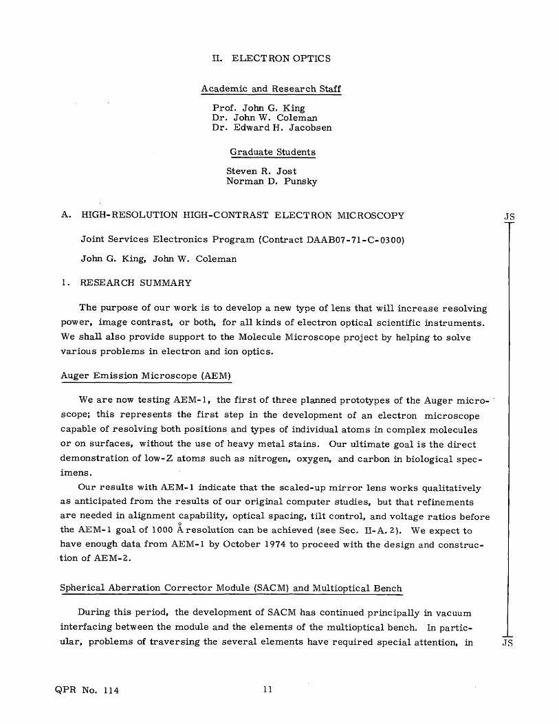
II. ELECTRON OPTICS
Academic and Research Staff
Prof. John G. KingDr. John W. ColemanDr. Edward H. Jacobsen
Graduate Students
Steven R. JostNorman D. Punsky
A. HIGH-RESOLUTION HIGH-CONTRAST ELECTRON MICROSCOPY JS
Joint Services Electronics Program (Contract DAAB07-71-C-0300)
John G. King, John W. Coleman
I. RESEARCH SUMMARY
The purpose of our work is to develop a new type of lens that will increase resolving
power, image contrast, or both, for all kinds of electron optical scientific instruments.
We shall also provide support to the Molecule Microscope project by helping to solve
various problems in electron and ion optics.
Auger Emission Microscope (AEM)
We are now testing AEM-1, the first of three planned prototypes of the Auger micro-
scope; this represents the first step in the development of an electron microscope
capable of resolving both positions and types of individual atoms in complex molecules
or on surfaces, without the use of heavy metal stains. Our ultimate goal is the direct
demonstration of low-Z atoms such as nitrogen, oxygen, and carbon in biological spec-
imens.
Our results with AEM-1 indicate that the scaled-up mirror lens works qualitatively
as anticipated from the results of our original computer studies, but that refinements
are needed in alignment capability, optical spacing, tilt control, and voltage ratios beforethe AEM-1 goal of 1000 A resolution can be achieved (see Sec. II-A. 2). We expect to
have enough data from AEM-1 by October 1974 to proceed with the design and construc-tion of AEM-2.
Spherical Aberration Corrector Module (SACM) and Multioptical Bench
During this period, the development of SACM has continued principally in vacuum
interfacing between the module and the elements of the multioptical bench. In partic-
ular, problems of traversing the several elements have required special attention, in JS
QPR No. 114
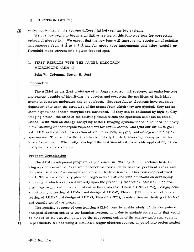
(II. ELECTRON OPTICS)
JS order not to disturb the vacuum differential between the two systems.
We are now ready to begin quantitative testing on this foil-type lens for correcting
spherical aberration. We expect that the new lens will improve the resolution of existing
microscopes from 8 A to 4-5 A and for probe-type instruments will allow twofold or
threefold more current into a given focused spot.
2. FIRST RESULTS WITH THE AUGER ELECTRON
MICROSCOPE (AEM-1)
John W. Coleman, Steven R. Jost
Introduction
The AEM-1 is the first prototype of an Auger electron microscope, an emission-type
instrument capable of identifying the species and resolving the positions of individual
atoms in complex molecules and on surfaces. Because Auger electrons have energies
dependent only upon the structure of the atoms from which they are ejected, they act as
atom signatures if their energies are measured. If they can be collected by high-quality
imaging optics, the sites of the emitting atoms within the specimen can also be estab-
lished. With such an energy-analyzing optical-imaging system, there is no need for heavy
metal staining or isomorphic replacement for low-Z atoms, and thus our ultimate goal
with AEM is the direct observation of atomic carbon, oxygen, and nitrogen in biological
specimens. The use of AEM is not fundamentally limited, however, to any particular
kind of specimen. When fully developed the instrument will have wide application, espe-
cially in materials science.
Program Organization
The AEM development program as proposed, in 1967, by E. H. Jacobsen to J. G.
King was concerned at first with theoretical research in several pertinent areas and
computer studies of wide-angle achromatic electron lenses. This research continued
until 1972 when a formally planned program was initiated with emphasis on developing
a prototype which was based initially upon the preceding theoretical studies. The pro-
gram was organized to be carried out in three phases: Phase 1 (1972-1974), design, con-
struction, and testing of AEM-1 and design of AEM-2; Phase 2 (1975), construction and
testing of AEM-2 and design of AEM-3; Phase 3 (1976), construction and testing of AEM-3
and completion of the program.
The specific purpose of constructing AEM-1 was to enable study of the computer-
designed electron optics of the imaging system, in order to exclude constraints that would
be placed on the electron optics by the subsequent optics of the energy-analyzing system.
JS In particular, we are using a simulated Auger electron source, injected into optics scaled
QPR No. 114
HEMISPHERICALBOSS
ELECTRODE
j~7 ciiK\
TYPICALTRAJECTORY
nI
ELECTRON BEAM FOR SECONDARY
ELECTRON EXCITATION
HOUSING
RING ELECTRODE (E6) -(- 18.0kV)
RING ELECTRODE (E5)(-22.0 kV)
RING ELECTRODE (E3)(TEMPORARILY GROUND)
RING ELECTRODE (El)(-18.0 kV)
RING ELECTRODE (EO)
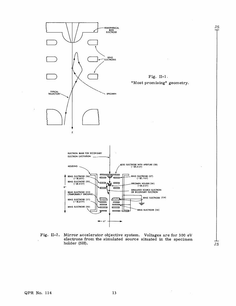
Fig. II-1.
"Most promising" geometry.
BOSS ELECTRODE WITH APERTURE (E8)(-20.0 kV)
RING ELECTRODE (E7)( -22.1 kV)
I amSPECIMEN HOLDER (SH)(-20.0 kV)
SIMULATED SOURCE ELECTRONOR SECONDARY ELECTRON
RING ELECTRODE (E4)
RING ELECTRODE (E2)
Fig. II-2. Mirror accelerator objective system. Voltages are for 300 eVelectrons from the simulated source situated in the specimenholder (SH).
QPR No. 114
f-' RING
S- ELECTRODES
I
S I
S\\ czMESPECIMEN
,-- 6 " o
C1
(II. ELECTRON OPTICS)
up to facilitate study of geometric tolerances and alignment. Energy analysis in AEM-1
is limited to that which is chromatically inherent in the imaging optics as a function of
input electron energy and lens voltages.
Construction of AEM-1
With the exclusion of the vacuum and electrical systems, the construction of AEM-1
has been implemented with the following design.
a. Mirror Accelerator Objective System
The geometry of this system is based upon the computer studies of Jacobsen and1 2
Ofsevit I and of Thomson which are related to the design of achromatic lenses with
extremely wide acceptance angles by the standards of conventional electron optics. These
lenses are wide cones of the order of 10* that have been seen heretofore only in visible
optics. The cylindrically symmetric geometry was selected as "most promising" for
the starting point, and the dimensions that we used (see Figs. II-1 and II-2) furnish
improvement by a factor of 4 over the dimensions given by computer. Because of the
scale factor and uncompensated spherical aberration, we expect resolution of only
~1000 A with AEM-1. This is not important in this phase of the program.
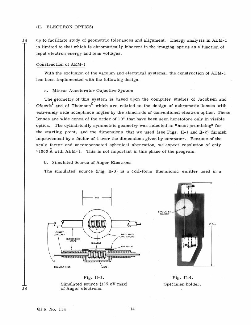
b. Simulated Source of Auger Electrons
The simulated source (Fig. II-3) is a coil-form thermionic emitter used in a
3mm
SIMULATED-,SOURCE
Fig. II-3.I Simulated source (325 eV max)JS of Auger electrons.
Fig. II-4.
Specimen holder.
QPR No. 114

(II. ELECTRON OPTICS)
miniature triode gun to send a spray of electrons of controllable energy into the mirror JS
accelerator objective system: The source rests in the specimen holder (SH) (Figs. II-2
and 11-4).
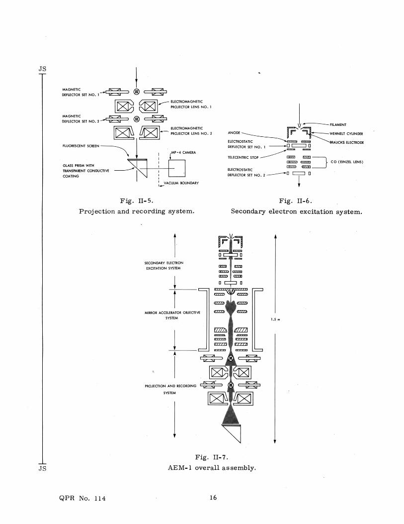
c. Projection Recording System
The projection recording system (Fig. II-5) has two sets of magnetic deflectors and
two magnetic lenses, with a final throw of 15 cm. This system, with a pick-up object
plane 6 cm in front of the gap of the first lens, allows variable magnification from
approximately 40-1970 X; further magnification ranges are possible if the position of the
pick-up plane is other than at 6 cm. The deflectors are for alignment, and the final image
is caught on a fluorescent screen on a glass prism. Photographs of the image are made
with an MP-4 Polaroid camera exterior to the vacuum.
d. Secondary Electron Excitation System
The secondary electron excitation system in AEM-1 (Fig. II-6) is the forerunner of
the Auger electron excitation system that will be used in AEM-2 and AEM-3. In AEM-1
the whole system is electrostatic. It is built from a Braucks-type electron gun, an Einzel
(unipotential) lens, and two sets of electrostatic deflectors. The excitation beam enters
the mirror accelerator objective system (see Fig. H1-2) by means of an aperture (E8) andis stopped by the specimen holder (SH). In this way, secondaries with a wide range of
energy may be sent through the mirror system, in contrast to electrons of a much nar-
rower range of energy which may be sent through with the simulated source.
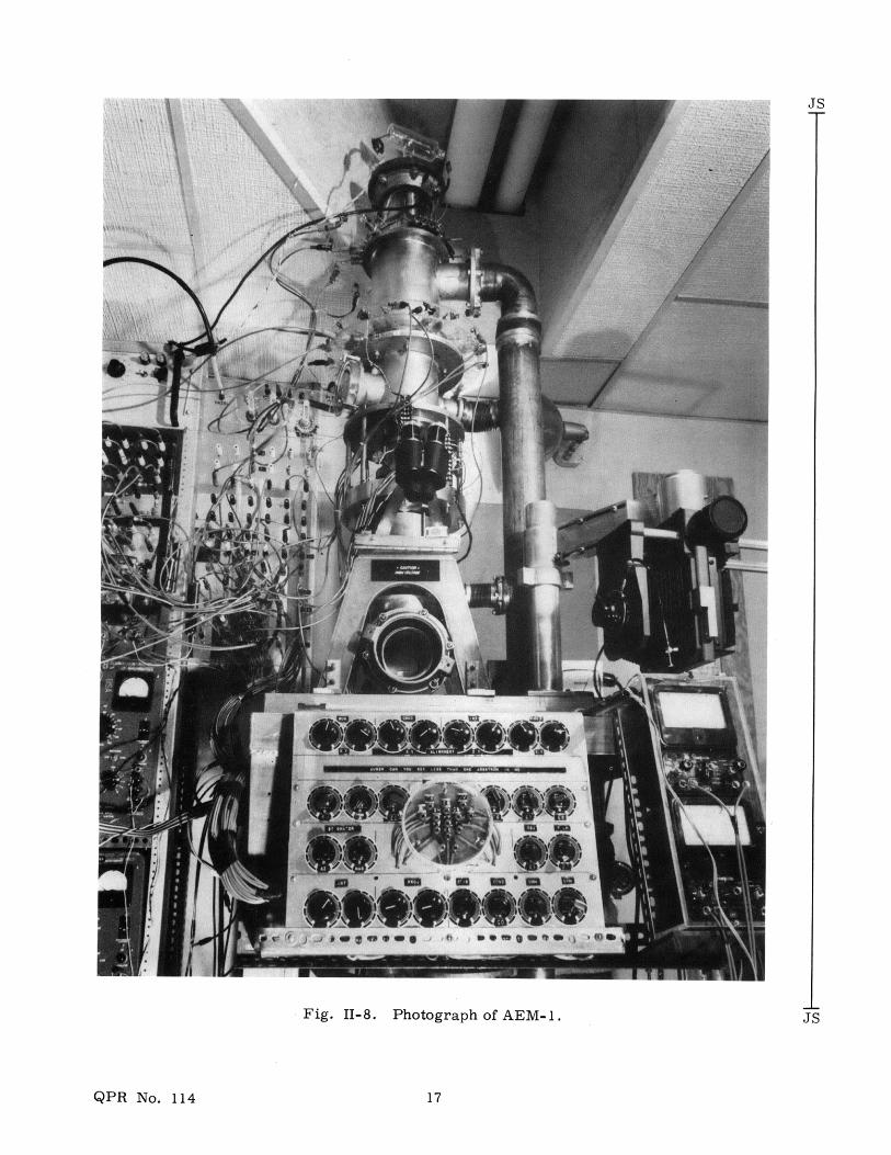
The overall assembly is shown schematically in Fig. 11-7, and a view of the instru-
ment is seen in Fig. 11-8.
Data Collection
We are now taking three kinds of data with AEM-1.
i. Focused and/or shadow images of grids (100-1500 mesh/inch) at selected sites
within the mirror accelerator objective system.
ii. Azimuthal intensity patterns (field energy profiles) measured from the fields
photographed from the fluorescent screen.
iii. Specular reflection patterns recorded by photographs of the fluorescent screen.
All photographs are tabulated on worksheets (Fig. II-9) and filed. In this way we areacquiring the hundreds of images that are necessary to gain statistically definitive knowl-
edge of the effects in the crucial areas of beam energy, electrode voltage, and sys-
tem alignment, including the effects of electrode machining tolerances, tilts, and JS
QPR No. 114
MAGNETIC
DEFLECTOR SET NO. I
ELECTROMAGNETIC
PROJECTOR LENS NO. 1
MAGNETIC
DEFLECTOR SET NO. 2
ELECTROMAGNETICPROJECTOR LENS NO. 2
FLUORESCENT SCREEN
P-4 CAMERA
GLASS PRISM WITH
TRANSPARENT CONDUCTIVE
COATING
Fig. II-5.
Projection and recording system.
S------ FILAMENT
ANODE r - WEHNELT CYLINDER
ELECTROSTATIC OE. "BRAUCRKS ELECTRODEDEFLECTOR SET NO. I 1
TELECENTRIC STOP -E2
c nm -2222 CO (EINZEL LENS)
ELECTROSTATIC
DEFLECTOR SET NO. 2 E
Fig. II-6.
Secondary electron excitation system.
SECONDARY ELECTRON
EXCITATION SYSTEM
MIRROR ACCELERATOR OBJECTIV
SYSTEM
PROJECTION AND RECORDING
SYSTEM
0E 0
V222=
ZCr=£2ZZZItzz
~P~cr"n
Fig. II-7.
AEM-1 overall assembly.
QPR No. 114
i
ncnnn=t
Ei~~~ .ile,;s; I-, i~*ilia
Z~ ~"S
~~~~is
~r
~ ""~
/W
Fig. 11-8. Photograph of AEM-1. JS
QPR No. 114
(II. ELECTRON OPTICS)
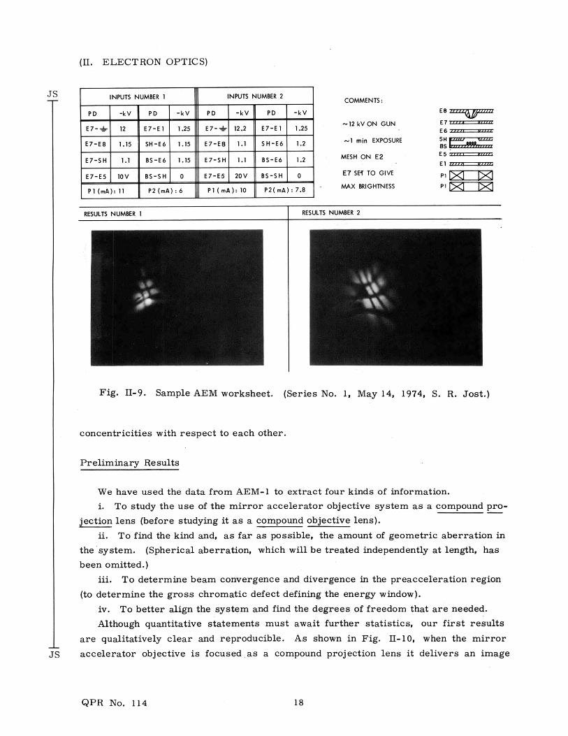
INPUTS NUMBER 1 INPUTS NUMBER 2
PD -kV PD -kV PD -kV PD -kV
E7-- 12 E7-E1 1.25 E7- 12.2 E7-E1 1.25
E7-E8 1.15 SH-E6 1.15 E7-E8 1.1 SH-E6 1.2
E7-SH 1.1 BS-E6 1.15 E7-SH 1.1 BS-E6 1.2
E7-E5 10V BS-SH 0 E7-E5 20V BS-SH 0
Pl (mA): 11 P2 (mA) : 6 Pl (mA): 10 P2(mA): 7.8
COMMENTS:
- 12 kV ON GUN
-1 min EXPOSURE
MESH ON E2
E7 SET TO GIVE
MAX BRIGHTNESS
E7E6
SHBS
P1 ZI
RESULTS NUMBER 1 RESULTS NUMBER 2
Fig. 11-9. Sample AEM worksheet. (Series No. 1, May 14, 1974, S. R. Jost.)
concentricities with respect to each other.
Preliminary Results
We have used the data from AEM-1 to extract four kinds of information.
i. To study the use of the mirror accelerator objective system as a compound pro-
jection lens (before studying it as a compound objective lens).
ii. To find the kind and, as far as possible, the amount of geometric aberration in
the system. (Spherical aberration, which will be treated independently at length, has
been omitted.)
iii. To determine beam convergence and divergence in the preacceleration region
(to determine the gross chromatic defect defining the energy window).
iv. To better align the system and find the degrees of freedom that are needed.
Although quantitative statements must await further statistics, our first results
are qualitatively clear and reproducible. As shown in Fig. II-10, when the mirror
JS accelerator objective is focused as a compound projection lens it delivers an image
QPR No. 114
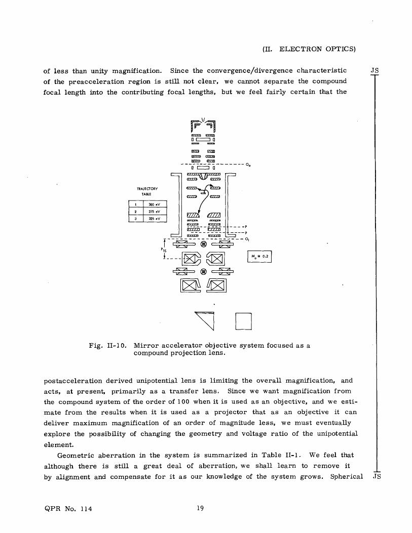
(II. ELECTRON OPTICS)
of less than unity magnification. Since the convergence/divergence characteristic
of the preacceleration region is still not clear, we cannot separate the compound
focal length into the contributing focal lengths, but we feel fairly certain that the
TRAJECTORY
TABLE
1 300 eV
2 275 eV
3 325 eV
o- V
-------------- PrV771 07M------ --------
a a777
P1S
~ ® cz
Ms 0.2
DFig. II-10. Mirror accelerator objective system focused as a
compound projection lens.
postacceleration derived unipotential lens is limiting the overall magnification, and
acts, at present, primarily as a transfer lens. Since we want magnification from
the compound system of the order of 100 when it is used as an objective, and we esti-
mate from the results when it is used as a projector that as an objective it can
deliver maximum magnification of an order of magnitude less, we must eventually
explore the possibility of changing the geometry and voltage ratio of the unipotential
element.
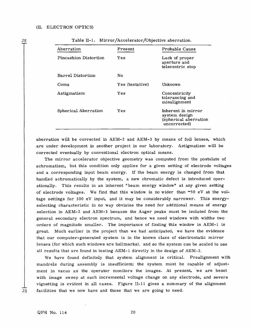
Geometric aberration in the system is summarized in Table II-1. We feel that
although there is still a great deal of aberration, we shall learn to remove it
by alignment and compensate for it as our knowledge of the system grows. Spherical JS
QPR No. 114
(II. ELECTRON OPTICS)
JS Table II-1. Mirror/Accelerator/Objective aberration.
Aberration Present Probable Cause
Pincushion Distortion Yes Lack of properaperture andtelecentric stop
Barrel Distortion No
Coma Yes (tentative) Unknown
Astigmatism Yes Concentricitytolerancing andmisalignment
Spherical Aberration Yes Inherent in mirrorsystem design(spherical aberrationuncorrected)
aberration will be corrected in AEM-2 and AEM-3 by means of foil lenses, which
are under development in another project in our laboratory. Astigmatism will be
corrected eventually by conventional electron optical means.
The mirror accelerator objective geometry was computed from the postulate of
achromatism, but this condition only applies for a given setting of electrode voltages
and a corresponding input beam energy. If the beam energy is changed from that
handled achromatically by the system, a new chromatic defect is introduced oper-
ationally. This results in an inherent "beam energy window" at any given setting
of electrode voltages. We find that this window is no wider than -50 eV at the vol-
tage settings for 300 eV input, and it may be considerably narrower. This energy-
selecting characteristic in no way obviates the need for additional means of energy
selection in AEM-Z and AEM-3 because the Auger peaks must be isolated from the
general secondary electron spectrum, and hence we need windows with widths two
orders of magnitude smaller. The importance of finding this window in AEM-1 is
great. Much earlier in the project than we had anticipated, we have the evidence
that our computer-generated system is in the known class of electrostatic mirror
lenses (for which such windows are hallmarks), and so the system can be scaled to use
all results that are found in testing AEM-1 directly in the design of AEM-2.
We have found definitely that system alignment is critical. Prealignment with
mandrels during assembly is insufficient; the system must be capable of adjust-
ment in vacuo as the operator monitors the images. At present, we are beset
with image sweep at each incremental voltage change on any electrode, and severe
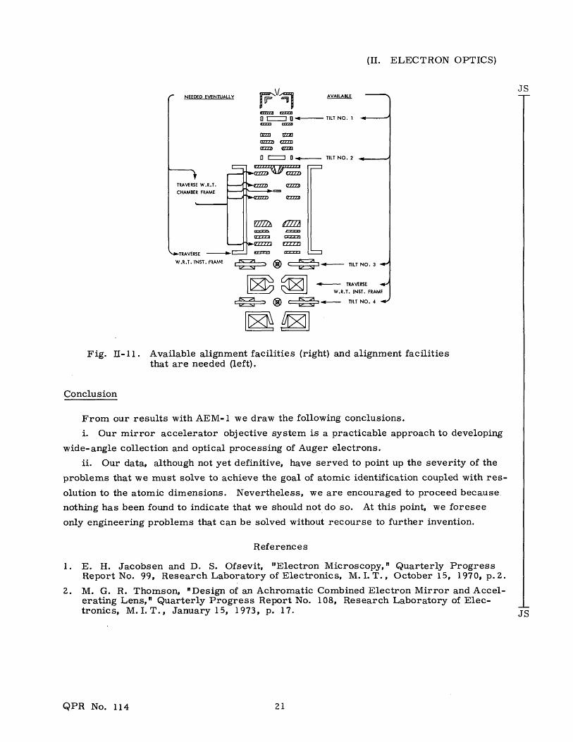
vignetting is evident in all cases. Figure II-11 gives a summary of the alignment
JS facilities that we now have and those that we are going to need.
QPR No. 114
(II. ELECTRON OPTICS)
NEEDED EVENTUALLY AVAILABLE S
0 : l 0 - TILT NO. I
n-71 r=-z
[zza Czzal
SCI 0 - TILT NO. 2
TRAVERSE W.R.T. Z
CHAMBER FRAME X -
TRAVERSE
W.R.T. INST. FRAME ® TILT NO. 3
TRAVERSE
W.R.T. INST. FRAME
E ® cm TILT NO. 4
Fig. II-11. Available alignment facilities (right) and alignment facilitiesthat are needed (left).
Conclusion
From our results with AEM-1 we draw the following conclusions.
i. Our mirror accelerator objective system is a practicable approach to developing
wide-angle collection and optical processing of Auger electrons.
ii. Our data, although not yet definitive, have served to point up the severity of the
problems that we must solve to achieve the goal of atomic identification coupled with res-
olution to the atomic dimensions. Nevertheless, we are encouraged to proceed because.
nothing has been found to indicate that we should not do so. At this point, we foresee
only engineering problems that can be solved without recourse to further invention.
References
1. E. H. Jacobsen and D. S. Ofsevit, "Electron Microscopy," Quarterly ProgressReport No. 99, Research Laboratory of Electronics, M. I. T., October 15, 1970, p. 2.
2. M. G. R. Thomson, "Design of an Achromatic Combined Electron Mirror and Accel-erating Lens," Quarterly Progress Report No. 108, Research Laboratory of Elec-tronics, M.I.T., January 15, 1973, p. 17. i
QPR No. 114