Embed Size (px)
Citation preview
III-V Compound Semiconductor Manufacturing in China: From Optoelectronic to Microwave Applications
Wenxin Chen, John Wang, Qingfang Zhu, Yanli Xu, Xiawei Zhong, Yishu Lin, Jungyi Peng,
Benjamin Li, Dan Tey, Binjun Cai, Taihui Liu, Zhidong Lin, and Kechuang Lin
Xiamen San’an Integrated Circuit Co., Ltd. 753-799 Minan Avenue, Xiamen 361110, China e-mail: [email protected]
Keywords: III-V, Foundry, HBT, pHEMT, GaN, SiC, and SBD Abstract Founded in 2000, San’an Optoelectronics Co., Ltd (SANAN) is the largest LED and CPV solar cell manufacturer in China. San’an-IC company (SAIC), a subsidiary company of San’an Group, was founded in 2014 as the first III-V compound semiconductor foundry in China. These two companies will cover a wide spectrum of III-V compound semiconductor product market in China, including LED, CPV, HBT, pHEMT and GaN applications. In this paper, the development in III-V compound materials and devices in San’an group will be presented. The current status along with the technology readiness in SAIC will also be reported. INTRODUCTION
The III-V compound semiconductors offer higher bandwidth, higher speed and higher power handling than IV materials such as Si and Ge [1, 2]. Properties and features like wide band gap, high frequency handling capability, operation at high temperatures, high current and breakdown voltage and direct band gap engineering have increased the usage of III-V semiconductors in various industrial applications, such as microwave RF, DC power and optical applications. There is an increased strong demand on III-V semiconductor technologies in optoelectronic devices, mobile and wireless devices in the past decade. China is the leading country in these applications in the world.
SANAN currently is the largest player for the top-
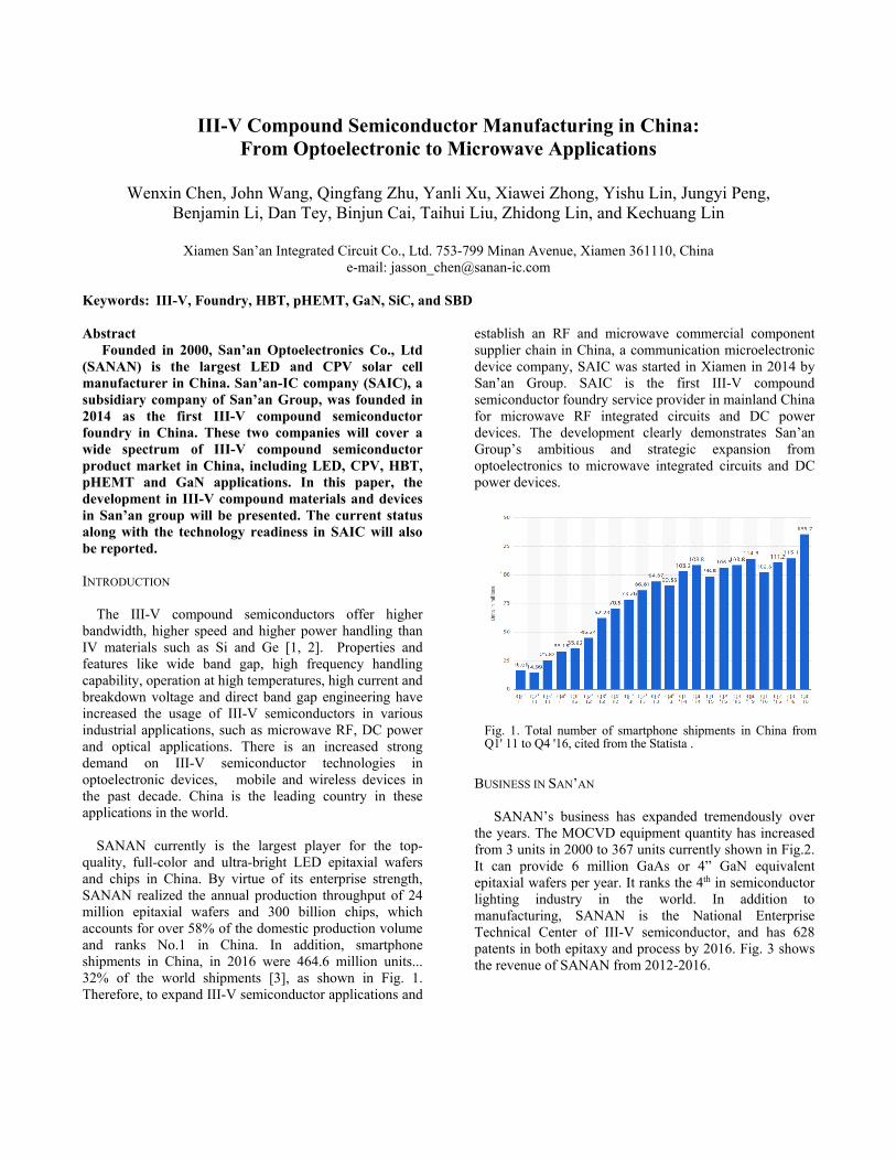
quality, full-color and ultra-bright LED epitaxial wafers and chips in China. By virtue of its enterprise strength, SANAN realized the annual production throughput of 24 million epitaxial wafers and 300 billion chips, which accounts for over 58% of the domestic production volume and ranks No.1 in China. In addition, smartphone shipments in China, in 2016 were 464.6 million units... 32% of the world shipments [3], as shown in Fig. 1. Therefore, to expand III-V semiconductor applications and
establish an RF and microwave commercial component supplier chain in China, a communication microelectronic device company, SAIC was started in Xiamen in 2014 by San’an Group. SAIC is the first III-V compound semiconductor foundry service provider in mainland China for microwave RF integrated circuits and DC power devices. The development clearly demonstrates San’an Group’s ambitious and strategic expansion from optoelectronics to microwave integrated circuits and DC power devices.
Fig. 1. Total number of smartphone shipments in China from Q1' 11 to Q4 '16, cited from the Statista .
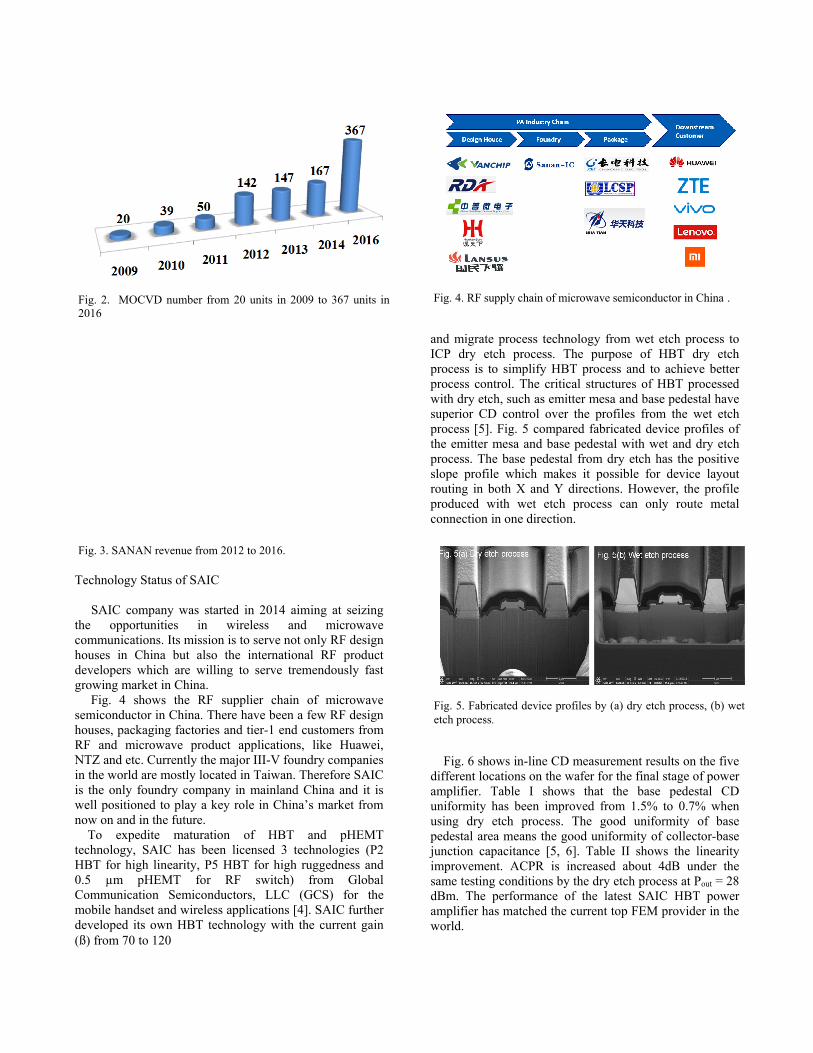
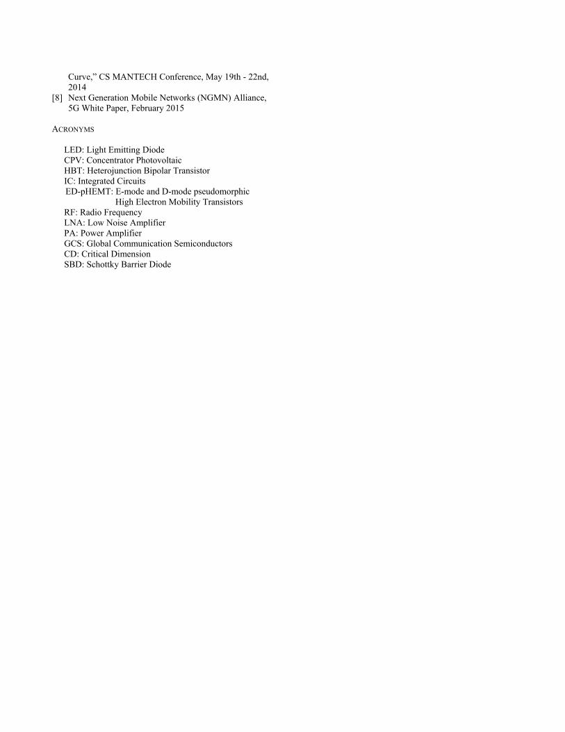
BUSINESS IN SAN’AN SANAN’s business has expanded tremendously over the years. The MOCVD equipment quantity has increased from 3 units in 2000 to 367 units currently shown in Fig.2. It can provide 6 million GaAs or 4” GaN equivalent epitaxial wafers per year. It ranks the 4th in semiconductor lighting industry in the world. In addition to manufacturing, SANAN is the National Enterprise Technical Center of III-V semiconductor, and has 628 patents in both epitaxy and process by 2016. Fig. 3 shows the revenue of SANAN from 2012-2016.
Technology Status of SAIC SAIC company was started in 2014 aiming at seizing the opportunities in wireless and microwave communications. Its mission is to serve not only RF design houses in China but also the international RF product developers which are willing to serve tremendously fast growing market in China.
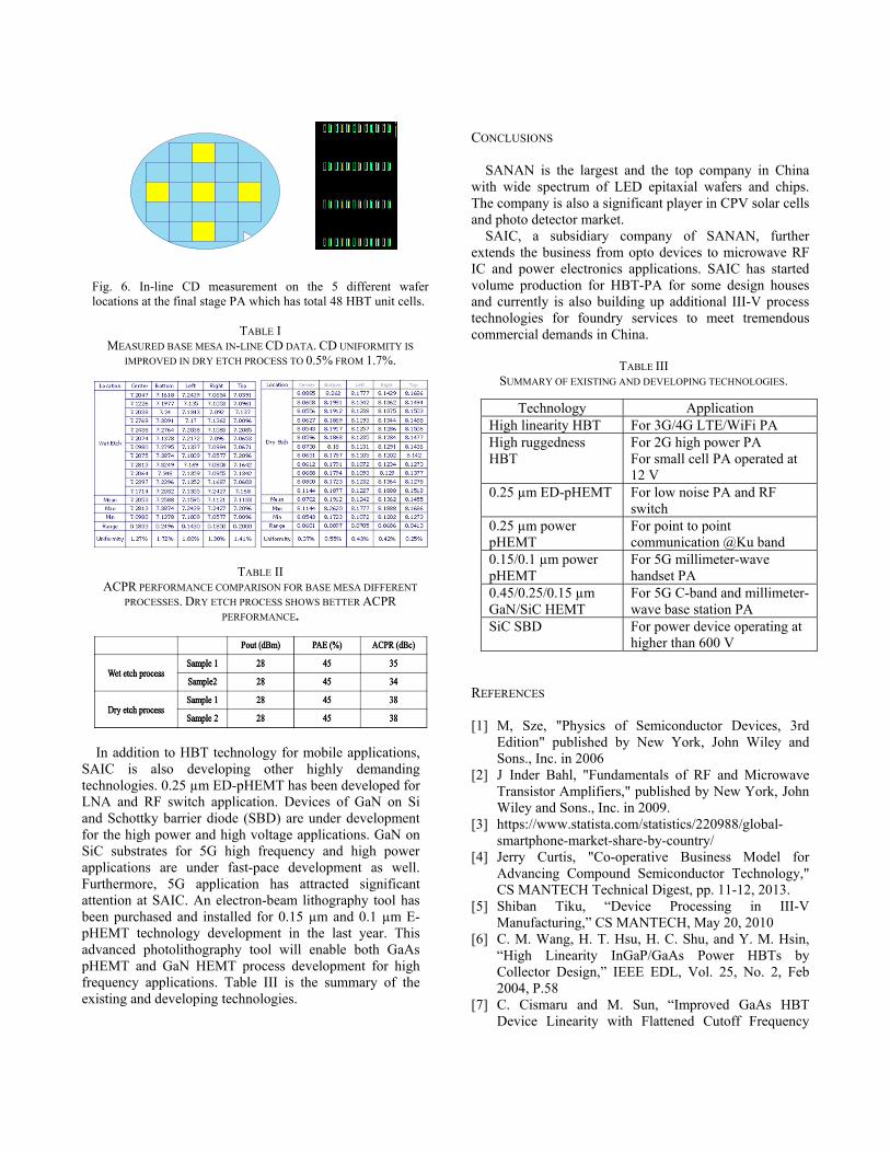
Fig. 4 shows the RF supplier chain of microwave semiconductor in China. There have been a few RF design houses, packaging factories and tier-1 end customers from RF and microwave product applications, like Huawei, NTZ and etc. Currently the major III-V foundry companies in the world are mostly located in Taiwan. Therefore SAIC is the only foundry company in mainland China and it is well positioned to play a key role in China’s market from now on and in the future.
To expedite maturation of HBT and pHEMT technology, SAIC has been licensed 3 technologies (P2 HBT for high linearity, P5 HBT for high ruggedness and 0.5 µm pHEMT for RF switch) from Global Communication Semiconductors, LLC (GCS) for the mobile handset and wireless applications [4]. SAIC further developed its own HBT technology with the current gain (ß) from 70 to 120
Fig. 4. RF supply chain of microwave semiconductor in China .
and migrate process technology from wet etch process to ICP dry etch process. The purpose of HBT dry etch process is to simplify HBT process and to achieve better process control. The critical structures of HBT processed with dry etch, such as emitter mesa and base pedestal have superior CD control over the profiles from the wet etch process [5]. Fig. 5 compared fabricated device profiles of the emitter mesa and base pedestal with wet and dry etch process. The base pedestal from dry etch has the positive slope profile which makes it possible for device layout routing in both X and Y directions. However, the profile produced with wet etch process can only route metal connection in one direction.
Fig. 6 shows in-line CD measurement results on the five
different locations on the wafer for the final stage of power amplifier. Table I shows that the base pedestal CD uniformity has been improved from 1.5% to 0.7% when using dry etch process. The good uniformity of base pedestal area means the good uniformity of collector-base junction capacitance [5, 6]. Table II shows the linearity improvement. ACPR is increased about 4dB under the same testing conditions by the dry etch process at Pout = 28 dBm. The performance of the latest SAIC HBT power amplifier has matched the current top FEM provider in the world.
Fig. 2. MOCVD number from 20 units in 2009 to 367 units in 2016
Fig. 3. SANAN revenue from 2012 to 2016.
Fig. 5. Fabricated device profiles by (a) dry etch process, (b) wet etch process.
In addition to HBT technology for mobile applications, SAIC is also developing other highly demanding technologies. 0.25 µm ED-pHEMT has been developed for LNA and RF switch application. Devices of GaN on Si and Schottky barrier diode (SBD) are under development for the high power and high voltage applications. GaN on SiC substrates for 5G high frequency and high power applications are under fast-pace development as well. Furthermore, 5G application has attracted significant attention at SAIC. An electron-beam lithography tool has been purchased and installed for 0.15 µm and 0.1 µm E-pHEMT technology development in the last year. This advanced photolithography tool will enable both GaAs pHEMT and GaN HEMT process development for high frequency applications. Table III is the summary of the existing and developing technologies.
CONCLUSIONS
SANAN is the largest and the top company in China with wide spectrum of LED epitaxial wafers and chips. The company is also a significant player in CPV solar cells and photo detector market.
SAIC, a subsidiary company of SANAN, further extends the business from opto devices to microwave RF IC and power electronics applications. SAIC has started volume production for HBT-PA for some design houses and currently is also building up additional III-V process technologies for foundry services to meet tremendous commercial demands in China.
TABLE III SUMMARY OF EXISTING AND DEVELOPING TECHNOLOGIES.
Technology Application High linearity HBT For 3G/4G LTE/WiFi PA High ruggedness HBT
For 2G high power PA For small cell PA operated at 12 V
0.25 µm ED-pHEMT For low noise PA and RF switch
0.25 µm power pHEMT
For point to point communication @Ku band
0.15/0.1 µm power pHEMT
For 5G millimeter-wave handset PA
0.45/0.25/0.15 µm GaN/SiC HEMT
For 5G C-band and millimeter-wave base station PA
SiC SBD For power device operating at higher than 600 V
REFERENCES [1] M, Sze, "Physics of Semiconductor Devices, 3rd
Edition" published by New York, John Wiley and Sons., Inc. in 2006
[2] J Inder Bahl, "Fundamentals of RF and Microwave Transistor Amplifiers," published by New York, John Wiley and Sons., Inc. in 2009.
[3] https://www.statista.com/statistics/220988/global-smartphone-market-share-by-country/
[4] Jerry Curtis, "Co-operative Business Model for Advancing Compound Semiconductor Technology," CS MANTECH Technical Digest, pp. 11-12, 2013.
[5] Shiban Tiku, “Device Processing in III-V Manufacturing,” CS MANTECH, May 20, 2010
[6] C. M. Wang, H. T. Hsu, H. C. Shu, and Y. M. Hsin, “High Linearity InGaP/GaAs Power HBTs by Collector Design,” IEEE EDL, Vol. 25, No. 2, Feb 2004, P.58
[7] C. Cismaru and M. Sun, “Improved GaAs HBT Device Linearity with Flattened Cutoff Frequency
Fig. 6. In-line CD measurement on the 5 different wafer locations at the final stage PA which has total 48 HBT unit cells.
TABLE I MEASURED BASE MESA IN-LINE CD DATA. CD UNIFORMITY IS
IMPROVED IN DRY ETCH PROCESS TO 0.5% FROM 1.7%.
TABLE II ACPR PERFORMANCE COMPARISON FOR BASE MESA DIFFERENT
PROCESSES. DRY ETCH PROCESS SHOWS BETTER ACPR
PERFORMANCE.
Curve,” CS MANTECH Conference, May 19th - 22nd, 2014
[8] Next Generation Mobile Networks (NGMN) Alliance, 5G White Paper, February 2015
ACRONYMS
LED: Light Emitting Diode CPV: Concentrator Photovoltaic HBT: Heterojunction Bipolar Transistor IC: Integrated Circuits ED-pHEMT: E-mode and D-mode pseudomorphic
High Electron Mobility Transistors RF: Radio Frequency LNA: Low Noise Amplifier PA: Power Amplifier GCS: Global Communication Semiconductors CD: Critical Dimension SBD: Schottky Barrier Diode