Embed Size (px)
Citation preview

103
Int. J. Engg. Res. & Sci. & Tech. 2015 xxxxxxxxxxxxxxxxxxxxxxxx, 2015
This article can be downloaded from http://www.ijerst.com/RASET-2015.php#1
SOFT-SWITCHING BIDIRECTIONAL
ISOLATED FULL-BRIDGE CONVERTER
WITH ACTIVE SNUBBERS
J Pushparaj1*, P Narendran1, D Selvakumar1 and D Deeban1
A bidirectional isolated full-bridge dc-dc converter with a conversion ratio around nine times, softstart-up, and soft-switching features for battery charging/discharging is proposed in this project.The converter is equipped with an active flyback snubbers, which can reduce voltage and currentspikes and reduce voltage and current stresses, while it can achieve near zero-voltage-switchingand zero-current-switching soft-switching features. In this paper, the operational principle of theproposed converter is first described, and its analysis and design are then presented.
Keywords: : Bidirectional dc-dc, Full bridge converter, Active snubbers, Zero voltage switching
*Corresponding Author: J Pushparaj � [email protected]
1 Department of Electrical Engineering, Jay shriram group of Institutions, Tirupur, Tamil Nadu, India.
Int. J. Engg. Res. & Sci. & Tech. 2015
Research Paper
INTRODUCTION
A conventional passive approach is employing a
resistor–capacitor–diode snubber to clamp the
voltage, and the energy absorbed in the buffer
capacitor is dissipated on the resistor, resulting
in low efficiency.It is hard switching system. In
this system Passive and active clamp circuits
were proposed to suppress the voltage spike due
to the current difference between the current-fed
inductor and leakage inductance currents. It is
soft switching system. The proposed converter
can reduce the voltage spike caused by the
current difference between leakage inductance
and current fed inductor currents, the current
spike due to diode reverse recovery, and the
current and voltage stresses, while it can achieve
near ZVS and ZCS soft-switching features.
BLOCK DIAGRAM: HARDWARE
ISSN 2319-5991 www.ijerst.com
Special Issue, Vol. 1, No. 2, April 2015
2nd National Conference on ‘‘Recent Advances in Science,
Engineering&Technologies’’ RASET-2015
© 2015 IJERST. All Rights Reserved
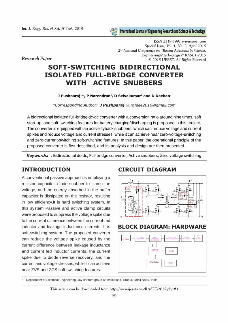
CIRCUIT DIAGRAM
104
Int. J. Engg. Res. & Sci. & Tech. 2015 J Pushparaj et al., 2015
This article can be downloaded from http://www.ijerst.com/RASET-2015.php#1
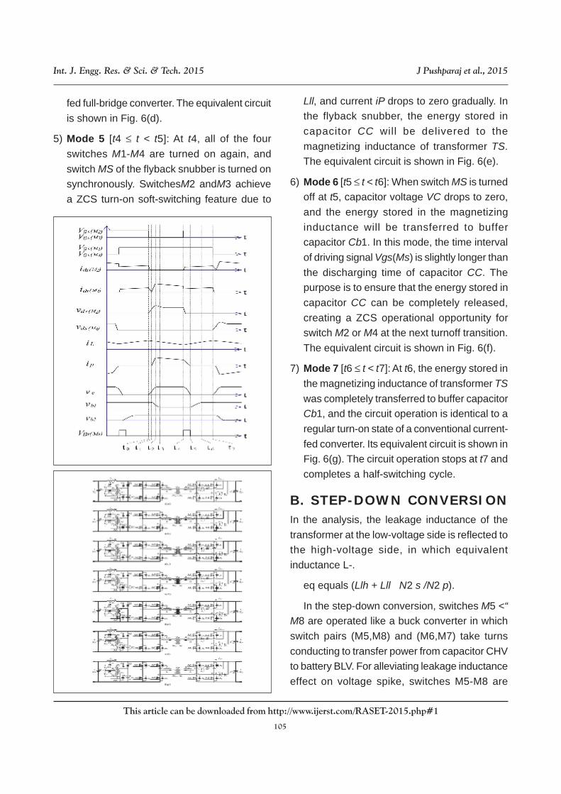
FORWARD DIRECTION capacitors Cb1 and Cb2. With the flybacksnubber, the energy absorbed in CC will not flowthrough switches M1-M4, which can reduce theircurrent stresses dramatically when the leakageinductance of the isolation transformer issignificant. The key voltage and currentwaveforms of the converter operated in the step-up conversion are shown in Fig. 5. A detaileddescription of the converter operation over a halfswitching cycle is presented as follows.
1) Mode 1 [t0 ≤ t < t1]: Before t0, all of the fourswitches M1-M4 are turned on. Inductor Lmis charged by VLV. At t0, M1 and M4 remainconducting, while M2 and M3 are turned off.Then, clamping diode DC conducts, andsnubber capacitor CC is charged by thecurrent difference iC. In this mode, the flybacksnubber still stays in the OFF state. Theequivalent circuit is shown in Fig. 6(a).
2) Mode 2 [t1 ≤ t < t2]: In this mode, leakageinductance current iP will start to track currentiL, and buffer capacitor Cb1 will start to releaseenergy. At time t2, current iP is equal to currentiL, the voltage of switches M2 and M3 andcapacitor CC will reach the maximum valuesimultaneously, and its equivalent circuit isshown in Fig. 6(b). A near ZCS soft switchingis therefore attained during t0 to t2.
3) Mode 3 [t2 ≤ t < t3]: Before t3, the energystored in buffer capacitor Cb1 is not fullydischarged yet. Thus, the capacitor will notstop discharging until Vb1 drops to zero. Theequivalent circuit is shown in Fig. 6(c).
4) Mode 4 [t3 ≤ t < t4]:When the energy storedin Cb1 has been completely released to theoutput at t3, diode D5 will conduct. The circuitoperation over this time interval is identical toa regular turnoff state of a conventional current-
CIRCUIT DIAGRAMA. Step-Up ConversionIn the step-up conversion, switches M1-M4 areoperated like a boost converter, where switchpairs (M1,M2) and (M3,M4) conduct to storeenergy in Lm. At the high-voltage side, body diodesD5-D8 of switchesM5-M8 will conduct to transferpower to CHV. When switch pairs (M1,M2) and(M3,M4) are switched to (M1,M4) or (M2,M3),current difference iC (= iL-iP ) will chargecapacitor CC until iP rises up to iL, and capacitorvoltage VC will be clamped to
VHV·(NP /NS), achieving near ZCS turnoff forM2 or M4. In the meantime, high-side current iShas the priority flowing through one of the twopassive capacitor–diode snubbers, and eitherCb1 or Cb2 will be fully discharged before diodeD5 or D7 conducts. When switch pair (M1,M4)or (M2,M3) is switched back to (M1,M2) and(M3,M4), switch M2 or M4 can have near ZCSturn-on feature due to leakage inductance Llllimiting the di/dt of high-side diode-reverse-recovery current. The flyback snubber operatessimultaneously to discharge snubber capacitorCC and transfer the stored energy to buffer
105
Int. J. Engg. Res. & Sci. & Tech. 2015 J Pushparaj et al., 2015
This article can be downloaded from http://www.ijerst.com/RASET-2015.php#1
fed full-bridge converter. The equivalent circuitis shown in Fig. 6(d).
5) Mode 5 [t4 ≤ t < t5]: At t4, all of the fourswitches M1-M4 are turned on again, andswitch MS of the flyback snubber is turned onsynchronously. SwitchesM2 andM3 achievea ZCS turn-on soft-switching feature due to
Lll, and current iP drops to zero gradually. Inthe flyback snubber, the energy stored incapacitor CC will be delivered to themagnetizing inductance of transformer TS.The equivalent circuit is shown in Fig. 6(e).
6) Mode 6 [t5 ≤ t < t6]: When switch MS is turnedoff at t5, capacitor voltage VC drops to zero,and the energy stored in the magnetizinginductance will be transferred to buffercapacitor Cb1. In this mode, the time intervalof driving signal Vgs(Ms) is slightly longer thanthe discharging time of capacitor CC. Thepurpose is to ensure that the energy stored incapacitor CC can be completely released,creating a ZCS operational opportunity forswitch M2 or M4 at the next turnoff transition.The equivalent circuit is shown in Fig. 6(f).
7) Mode 7 [t6 ≤ t < t7]: At t6, the energy stored inthe magnetizing inductance of transformer TSwas completely transferred to buffer capacitorCb1, and the circuit operation is identical to aregular turn-on state of a conventional current-fed converter. Its equivalent circuit is shown inFig. 6(g). The circuit operation stops at t7 andcompletes a half-switching cycle.
B. STEP-DOWN CONVERSIONIn the analysis, the leakage inductance of thetransformer at the low-voltage side is reflected tothe high-voltage side, in which equivalentinductance L-.
eq equals (Llh + Lll · N2 s /N2 p).
In the step-down conversion, switches M5 <“M8 are operated like a buck converter in whichswitch pairs (M5,M8) and (M6,M7) take turnsconducting to transfer power from capacitor CHVto battery BLV. For alleviating leakage inductanceeffect on voltage spike, switches M5-M8 are
106
Int. J. Engg. Res. & Sci. & Tech. 2015 J Pushparaj et al., 2015
This article can be downloaded from http://www.ijerst.com/RASET-2015.php#1
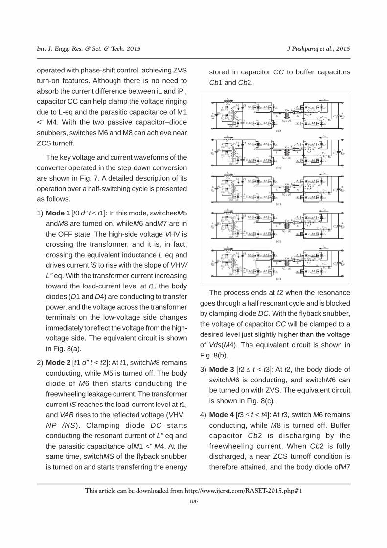
operated with phase-shift control, achieving ZVSturn-on features. Although there is no need toabsorb the current difference between iL and iP ,capacitor CC can help clamp the voltage ringingdue to L-eq and the parasitic capacitance of M1<“ M4. With the two passive capacitor–diodesnubbers, switches M6 and M8 can achieve nearZCS turnoff.
The key voltage and current waveforms of theconverter operated in the step-down conversionare shown in Fig. 7. A detailed description of itsoperation over a half-switching cycle is presentedas follows.
1) Mode 1 [t0 d” t < t1]: In this mode, switchesM5andM8 are turned on, whileM6 andM7 are inthe OFF state. The high-side voltage VHV iscrossing the transformer, and it is, in fact,crossing the equivalent inductance L eq anddrives current iS to rise with the slope of VHV/L” eq. With the transformer current increasingtoward the load-current level at t1, the bodydiodes (D1 and D4) are conducting to transferpower, and the voltage across the transformerterminals on the low-voltage side changesimmediately to reflect the voltage from the high-voltage side. The equivalent circuit is shownin Fig. 8(a).
2) Mode 2 [t1 d” t < t2]: At t1, switchM8 remainsconducting, while M5 is turned off. The bodydiode of M6 then starts conducting thefreewheeling leakage current. The transformercurrent iS reaches the load-current level at t1,and VAB rises to the reflected voltage (VHV ·NP /NS). Clamping diode DC startsconducting the resonant current of L” eq andthe parasitic capacitance ofM1 <“ M4. At thesame time, switchMS of the flyback snubberis turned on and starts transferring the energy
stored in capacitor CC to buffer capacitorsCb1 and Cb2.
The process ends at t2 when the resonancegoes through a half resonant cycle and is blockedby clamping diode DC. With the flyback snubber,the voltage of capacitor CC will be clamped to adesired level just slightly higher than the voltageof Vds(M4). The equivalent circuit is shown inFig. 8(b).
3) Mode 3 [t2 ≤ t < t3]: At t2, the body diode ofswitchM6 is conducting, and switchM6 canbe turned on with ZVS. The equivalent circuitis shown in Fig. 8(c).
4) Mode 4 [t3 ≤ t < t4]: At t3, switch M6 remainsconducting, while M8 is turned off. Buffercapacitor Cb2 is discharging by thefreewheeling current. When Cb2 is fullydischarged, a near ZCS turnoff condition istherefore attained, and the body diode ofM7
107
Int. J. Engg. Res. & Sci. & Tech. 2015 J Pushparaj et al., 2015
This article can be downloaded from http://www.ijerst.com/RASET-2015.php#1
then starts conducting the freewheelingcurrent. The equivalent circuit is shown in Fig.8(d).
5) Mode 5 [t4 ≤ t < t5]: At t4, with the body diodeof switch M7 conducting, M7 can be turnedon with ZVS. Over this time interval, the activeswitches change to the other pair of switches,and the voltage across the transformerreverses its polarity. The circuit operationstops at t5 and completes a half-switchingcycle. The equivalent circuit is shown in Fig.8(e).
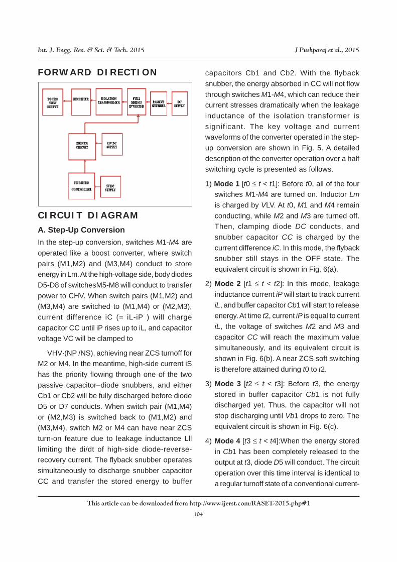
HARDWARE DETAILSDriver CircuitIt is used to provide 5 to 12 volts to switch theMOSFET Switches of the inverter. Driveramplifies the voltage from microcontroller whichis 5volts. Also it has an optocoupler for isolatingpurpose. So damage to MOSFET is prevented.
HOW THEY’RE USEDBasically the simplest way to visualize anoptocoupler is in terms of its two maincomponents: the input LED and the outputtransistor or diac. As the two are electricallyisolated, this gives a fair amount of flexibility whenit comes to connecting them into circuit. All wereally have to do is work out a convenient way ofturning the input LED on and off, and using theresulting switching of the phototransistor/ diacto generate an output waveform or logic signalthat is compatible with our output circuitry.
For example: just like a discrete LED, you candrive an optocoupler’s input LED from atransistor or logic gate/buffer. All that’s needed isa series resistor to set the current level whenthe LED is turned on. And regardless of whetheryou use a transistor or logic buffer to drive theLED, you still have the option of driving it in pulldown or pull up mode. This means you canarrange for the LED, and hence the optocoupler,to be either on or off, for a logic high (or low) inthe driving circuitry. In some circuits, there maybe a chance that at times the driving voltage fedto the input LED could have reversed polarity(due to a swapped cable connection, for
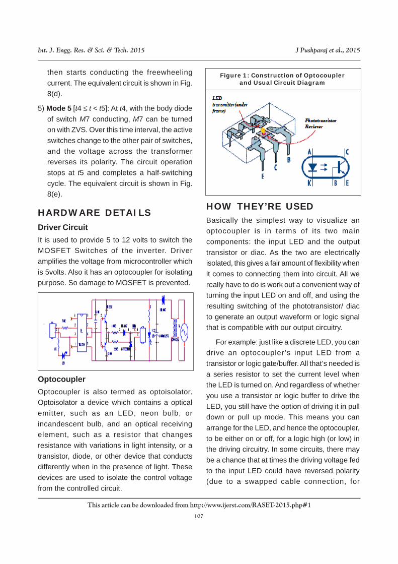
OptocouplerOptocoupler is also termed as optoisolator.Optoisolator a device which contains a opticalemitter, such as an LED, neon bulb, orincandescent bulb, and an optical receivingelement, such as a resistor that changesresistance with variations in light intensity, or atransistor, diode, or other device that conductsdifferently when in the presence of light. Thesedevices are used to isolate the control voltagefrom the controlled circuit.
Figure 1: Construction of Optocouplerand Usual Circuit Diagram

108
Int. J. Engg. Res. & Sci. & Tech. 2015 J Pushparaj et al., 2015
This article can be downloaded from http://www.ijerst.com/RASET-2015.php#1
example). This can cause damage to the device,because optocoupler LED’s tend to have quite alow reverse voltage rating: typically only 3 - 5V.So if this is a possibility, a reversed polarity diodeshould be connected directly across the LED asshown in Fig.3. On the output side, there are againa number of possible connections even with atypical optocoupler of the type having a singlephototransistor receiver (such as the 4N25 or4N28). In most cases the transistor is simplyconnected as a light-operated switch, in serieswith a load resistor RL (see Fig.4). The base ofthe transistor is left unconnected, and the choiceis between having the transistor at the top of theload resistor (Fig.4A) or at the bottom (Fig.4B).i.e., in either pull-up or pull-down mode. This againgives plenty of flexibility for driving either logicgates or transistors, as shown in Fig.5. If higherbandwidth is needed, it can be achieved by usingonly the collector and base connections, and byusing the transistor as a photodiode (Fig.6A). Thislowers the optocoupler’s CTR and transfer gainconsiderably, but can increase the bandwidth to30MHz or so.
An alternative approach is still to use the outputdevice as a phototransistor, but tie the base downto ground (or the emitter) via a resistor Rb, toassist in removal of stored charge (Fig.6B). Thiscan extend the opto’s bandwidth usefully(although not dramatically), without lowering theCTR and transfer gain any more than isnecessary. Typically you’d start with a resistorvalue of 1MW, and reduce it gradually down toabout 47kW to see if the desired bandwidth canbe reached.
Triggering UnitPIC 16F877A Microcontroller
INTRODUCTIONWe are using PIC 16F877A for producingswitching pulses to multilevel inverter. so as touse those vectors which do not generate anycommon mode voltage at the inverter poles. .Thiseliminates common mode voltage Also it is usedto eliminate capacitor voltage unbalancing. Themicrocontroller are driven via the driver circuit soas to boost the voltage triggering signal to 9V.Toavoid any damage to micro controller due to directpassing of 230V supply to it we provide an isolatorin the form of optocoupler in the same drivercircuit.
FEATURES OF PICMICROCONTROLLERThe microcontroller has the following features:
1. High-Performance RISC CPU
• Only 35 single- word instructions to learn.Hence it is user friendly.easy to use
• All single - cycle instructions except forprogram branches, which are two-cycle
• Operating speed: DC – 20 MHz clock inputDC – 200 ns instruction cycle
• Up to 8K x 14 words of Flash Program Memory,Up to 368 x 8 bytes of Data Memory(RAM), Upto 256 x 8 bytes of EEPROM Data Memory. Itis huge one
2. Peripheral Features
• Timer0: 8-bit timer/counter with 8 – bitprescaler. It is used for synchronisation
• Timer1: 16-bit timer/counter with prescaler, canbe incremented during Sleep
109
Int. J. Engg. Res. & Sci. & Tech. 2015 J Pushparaj et al., 2015
This article can be downloaded from http://www.ijerst.com/RASET-2015.php#1
• Timer2:8-bit timer/counter with 8-bit periodregister, prescaler and postscaler
• Two Capture , Compare and some PWMmodules, having following features
• Capture is 16-bit, max. resolution is 12.5 ns
• Compare is 16-bit, max . resolution is 200 ns
• PWM maximum resolution that is 10-bit
3. Synchronous Serial Port (SSP) with SPI(Master mode) and I2C(Master/Slave)
• Universal Synchronous AsynchronousReceiver Transmitter with 9 bit address
• Parallel Slave Port (PSP) 8 bits wide withexternal RD, WR and CS controls
4. Analog features
It has an analog Comparator module with:
• Two analog comparators
• Programmable on-chip voltage reference(VREF) module (3)Programmable inputmultiplexing from device inputs and internalvoltage reference thus 3 parts.
5. CMOS Technology
It has following features:
• Low-power, high-speed Flash/EEPROMtechnology
• Fully static design
• Wide operating voltage range (2.0V to 5.5V)
• Commercial and Industrial temperatureranges
• Low-power consumption
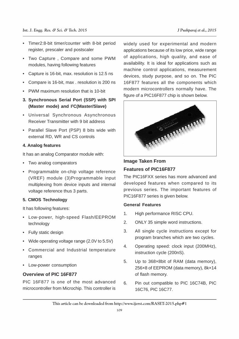
Overview of PIC 16F877PIC 16F877 is one of the most advancedmicrocontroller from Microchip. This controller is
widely used for experimental and modernapplications because of its low price, wide rangeof applications, high quality, and ease ofavailability. It is ideal for applications such asmachine control applications, measurementdevices, study purpose, and so on. The PIC16F877 features all the components whichmodern microcontrollers normally have. Thefigure of a PIC16F877 chip is shown below.
Image Taken FromFeatures of PIC16F877The PIC16FXX series has more advanced anddeveloped features when compared to itsprevious series. The important features ofPIC16F877 series is given below.
General Features
1. High performance RISC CPU.
2. ONLY 35 simple word instructions.
3. All single cycle instructions except forprogram branches which are two cycles.
4. Operating speed: clock input (200MHz),instruction cycle (200nS).
5. Up to 368×8bit of RAM (data memory),256×8 of EEPROM (data memory), 8k×14of flash memory.
6. Pin out compatible to PIC 16C74B, PIC16C76, PIC 16C77.

110
Int. J. Engg. Res. & Sci. & Tech. 2015 J Pushparaj et al., 2015
This article can be downloaded from http://www.ijerst.com/RASET-2015.php#1
7. Eight level deep hardware stack.
8. Interrupt capability (up to 14 sources)
9. Different types of addressing modes (direct,Indirect, relative addressing modes).
10. Power on Reset (POR).
11. Power-Up Timer (PWRT) and oscillatorstart-up timer.
12. Low power- high speed CMOS flash/EEPROM.
13. Fully static design.
14. Wide operating voltage range (2.0 –5.56)volts.
Peripheral Features
1. Timer 0: 8 bit timer/counter with pre-scalar.
2. Timer 1:16 bit timer/counter with pre-scalar.
3. Timer 2: 8 bit timer/counter with 8 bit periodregisters with pre-scalar and post-scalar.
4. Two Capture (16bit/12.5nS), Compare (16bit/200nS), Pulse Width Modules (10bit).
5. 10bit multi-channel A/D converter
6. Synchronous Serial Port (SSP) with SPI(master code) and I2C (master/slave).
7. Universal Synchronous AsynchronousReceiver Transmitter (USART) with 9 bitaddress detection.
8. Parallel Slave Port (PSP) 8 bit wide withexternal RD, WR and CS controls (40/46pin).
9. Brown Out circuitry for Brown-Out Reset(BOR).
Key Features
1. Maximum operating frequency is 20MHz.
2. Flash program memory (14 bit words), 8KB.
3 Data memory (bytes) is 368.
4. EEPROM data memory (bytes) is 256.
5. 5 input/output ports.-
6. 3 timers.
7. 2 CCP modules.
8. 2 serial communication ports (MSSP,USART).
9. PSP parallel communication port
10. 10bit A/D module (8 channels)
Analog Features
1. 10bit, up to 8 channel A/D converter.
2. Brown Out Reset function.
3. Analog comparator module.
Special Features
1. 100000 times erase/write cycle enhancedmemory.
2. 1000000 times erase/write cycle dataEEPROM memory.
3. Self programmable under software control.
4. In-circuit serial programming and in-circuitdebugging capability.
5. Single 5V,DC supply for circuit serialprogramming
6. WDT with its own RC oscillator for reliableoperation.
7. Programmable code protection.
8. Power saving sleep modes.
9. Selectable oscillator options.
PIN DIAGRAMSPIC16F877 chip is available in different types ofpackages. According to the type of applications

111
Int. J. Engg. Res. & Sci. & Tech. 2015 J Pushparaj et al., 2015
This article can be downloaded from http://www.ijerst.com/RASET-2015.php#1
and usage, these packages are differentiated. Thepin diagrams of a PIC16F877 chip in differentpackages is shown in the figure below.
• Every falling edge
• Every rising edge
• Every 4th rising edge
• Every 16th rising edge
The type of event is configured by control bits,CCP1M3:CCP1M0 (CCPxCON<3:0>). When acapture is made, the interrupt request flag bit,CCP1IF (PIR1<2>), is set. The interrupt flag mustbe cleared in software. If another capture occursbefore the value in register CCPR1 is read, theold captured value is overwritten by the new value.The block diagram of
MATLAB
Circuit Diagram
Forward Control
Figure: PIC Microcontroller Pin Diagram
CCP1 ModuleCapture/Compare/PWM Register 1 (CCPR1) isa 16 bit register comprised of two 8-bit registers:CCPR1L (low byte) and CCPR1H (high byte). TheCCP1CON register controls the operation ofCCP1. The special event trigger is generated bya compare match and will reset Timer1.
CCP2 ModuleCapture/Compare/PWM Register 2 (CCPR2) iscomprised of two 8-bit registers: CCPR2L (lowbyte) and CCPR2H (high byte). The CCP2CONregister controls the operation of CCP2. Thespecial event trigger is generated by a comparematch and will reset Timer1 and start an A/Dconversion (if the A/D module is enabled).
Capture ModeIn Capture mode, CCPR1H:CCPR1L capturesthe 16-bit value of the TMR1 register when anevent occurs on pin RC2/CCP1.
An event is defined as one of the following:
Output Waveform
112
Int. J. Engg. Res. & Sci. & Tech. 2015 J Pushparaj et al., 2015
This article can be downloaded from http://www.ijerst.com/RASET-2015.php#1
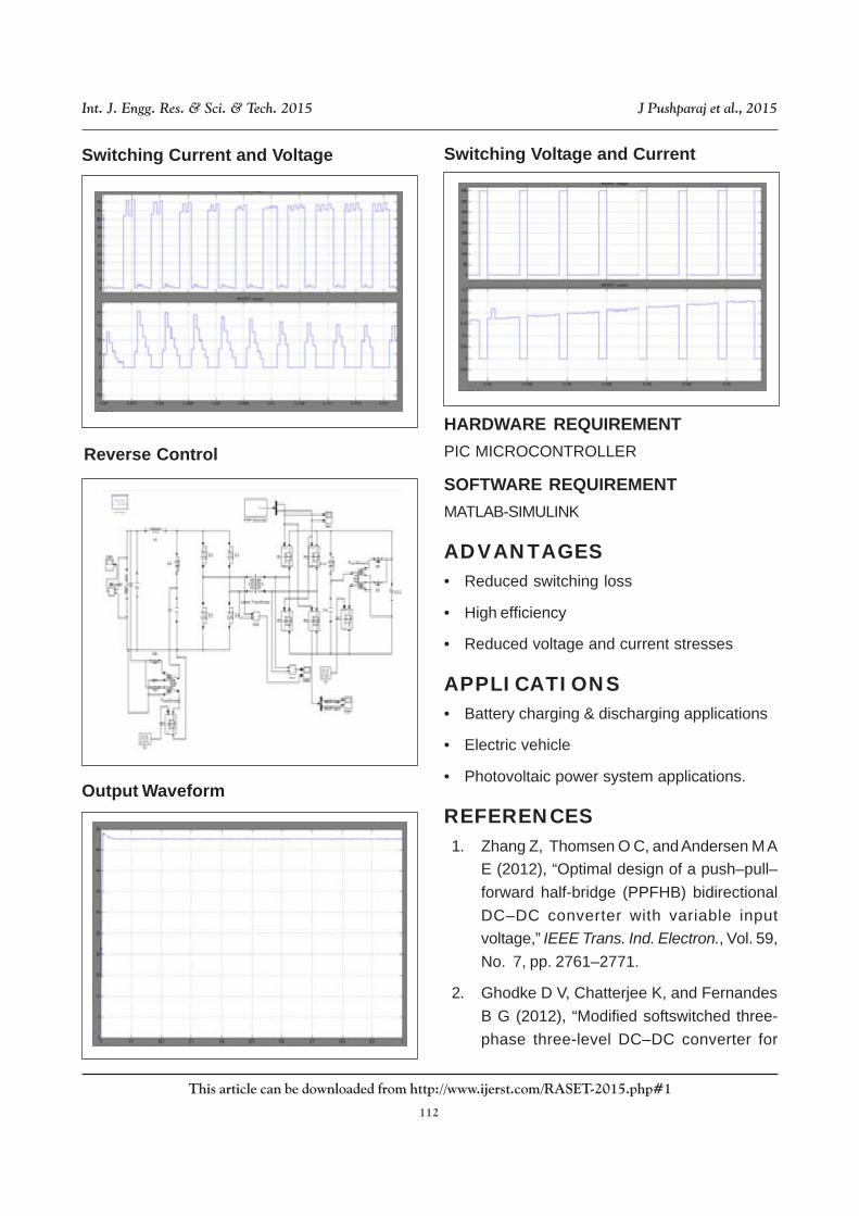
Switching Current and Voltage
Reverse Control
Output Waveform
Switching Voltage and Current
HARDWARE REQUIREMENTPIC MICROCONTROLLER
SOFTWARE REQUIREMENTMATLAB-SIMULINK
ADVANTAGES• Reduced switching loss
• High efficiency
• Reduced voltage and current stresses
APPLICATIONS• Battery charging & discharging applications
• Electric vehicle
• Photovoltaic power system applications.
REFERENCES1. Zhang Z, Thomsen O C, and Andersen M A
E (2012), “Optimal design of a push–pull–forward half-bridge (PPFHB) bidirectionalDC–DC converter with variable inputvoltage,” IEEE Trans. Ind. Electron., Vol. 59,No. 7, pp. 2761–2771.
2. Ghodke D V, Chatterjee K, and FernandesB G (2012), “Modified softswitched three-phase three-level DC–DC converter for

113
Int. J. Engg. Res. & Sci. & Tech. 2015 J Pushparaj et al., 2015
This article can be downloaded from http://www.ijerst.com/RASET-2015.php#1
high-power applications having extendedduty cycle range,” IEEE Trans. Ind.Electron., Vol. 59, No. 9, pp. 3362–3372.
3. Zhang F, Xiao L, and Yan Y (2004), “Bi-directional forward-flyback DC–DCconverter,” in Proc. IEEE Power Electron.Spec. Conf., Vol. 5, pp. 4058–4061.
4. Li H, Liu D, Peng F Z, and Su G J (2005),
“Small signal analysis of a dual half bridgeisolated ZVS bi-directional DC–DCconverter for electrical vehicle applications,”in Proc. IEEE Power Electron. Spec. Conf.,pp. 2777–2782.
5. Yang L S and Liang T J (2012), “Analysisand implementation of a novel bidirectionalDC–DC converter,” IEEE Trans. Ind.Electron., Vol. 59, No. 1, pp. 422–434.


![HIGH-CONVERSION-RATIO BIDIRECTIONAL DC–DC ......bidirectional dc –dc converter with a high convention ratio is a key component of battery applications [5] Isolated bidirectional](https://img.pdfslide.net/doc/110x75/5f0a32787e708231d42a7b2d/high-conversion-ratio-bidirectional-dcadc-bidirectional-dc-adc-converter.jpg)