Embed Size (px)
Citation preview

ILT for Double Exposure Lithography with Conventional and
Novel Materials
Amyn Poonawalaa and Yan Borodovskyb and Peyman Milanfarc
aDepartment of Computer Engineering, University of California, Santa Cruz, USAbPortland Technology Development, Intel Corporation, Hillsboro, USA
cDepartment of Electrical Engineering, University of California, Santa Cruz, USA
ABSTRACT
Multiple paths exists to provide lithography solutions pursuant to Moore’s Law for next 3-5 generations oftechnology, yet each of those paths inevitably leads to solutions eventually requiring patterning at k1 < 0.30and below. In this article, we explore double exposure single development lithography for k1 ≥ 0.25 (usingconventional resist) and k1 < 0.25 (using new out-of-sight out-of-mind materials). For the case of k1 ≥ 0.25, wepropose a novel double exposure inverse lithography technique (ILT) to split the pattern. Our algorithm is basedon our earlier proposed single exposure ILT framework, and works by decomposing the aerial image (instead ofthe target pattern) into two parts. It also resolves the phase conflicts automatically as part of the decomposition,and the combined aerial image obtained using the estimated masks has a superior contrast.
For the case of k1 < 0.25, we focus on analyzing the use of various dual patterning techniques enabled by theuse of hypothetic materials with properties that allow for the violation of the linear superposition of intensitiesfrom the two exposures. We investigate the possible use of two materials: contrast enhancement layer (CEL) andtwo-photon absorption resists. We propose a mathematical model for CEL, define its characteristic properties,and derive fundamental bounds on the improvement in image log-slope. Simulation results demonstrate thatdouble exposure single development lithography using CEL enables printing 80nm gratings using dry lithography.We also combine ILT, CEL, and DEL to synthesize 2-D patterns with k1 = 0.185. Finally, we discuss the viabilityof two-photon absorption resists for double exposure lithography.
Keywords: Double exposure lithography, inverse lithography, CEL, two-photon absorption resist, ILS.
1. INTRODUCTION AND BACKGROUND
Double exposure lithography is considered an important road-map enabler for 32nm and smaller nodes. Doubleexposure can be broadly classified into two categories depending on the number of times the resist is developed.In the single development case, two (same or different) masks and two (same or different) illumination settingsare used in order to print the desired circuit pattern. If a conventional resist is used, the final aerial image isthe linear super-position of the two individual exposures. Hence, the minimum resolvable pitch is the same assingle-exposure, i.e., minimum kpitch = 0.5 and
Min Pitch = 0.5λ
NA. (1)
The above technique is known to give superior contrast for low k1 values and finds applications such as trim maskwith alternating phase shift masks (PSM),5 double dipole lithography, IDEAL (Innovative Double Exposure byAdvanced Lithography),7 etc.
The double development case (also referred to as dual patterning) requires an additional resist development,etching, and coating steps in between the two exposures.4, 8 The concept behind multiple exposure/develop
a E-mail: [email protected] E-mail: [email protected] E-mail: [email protected]

techniques is that the fundamental single-exposure limit given in (1) is not on the individual feature size (CD),but on the pattern pitch.1 Using non-linearities in the pattern transfer process, CDs can be much smallerthan the half of the smallest allowed pitch. Dual patterning uses the above concept by patterning features atdimensions close to 1/4 of the minimal pitch allowed by constrains of imaging system, and stores the informationfrom the first exposure in a hard mask (or other sacrificial layer). The second exposure is then carried outwith similar feature size target and appropriate shift and again preserved in sacrificial layer, thereby doublingthe frequency of each exposed features present on each of the masks. The minimum pitch resolution for dualpatterning is 0.25 λ
NA. It was demonstrated that dual patterning allows one to reach patterning with effective k1
as low as 0.16.12
However, additional processing steps related to preserving image of the first exposure in sacrificial layer(such as need to load and unload wafer twice from the exposure tool), carry additional overlay and dimensionalcontrol (CD) penalty. Furthermore, the extra processing steps such as second develop, hard-mask deposition,and etch steps might result in additional yield liability as well as increased wafer cost. There is strong incentiveto identify techniques capable to support patterning with two masks containing split design information, yetcapable of producing combined final latent image in resist without unloading the wafer off the exposure toolchunk. We thus need only one single exposure to produce image ready for pitch doubling, thereby avoiding theneed for sacrificial layer, the follow-up processing steps, and their corresponding yield liabilities.
In this article, we exclusively focus on double exposure single development lithography (hence referred to asDEL). The paper considers two cases of DEL. The first case employs DEL to pattern with high contrast logicpattern at low k1 values between 0.25 and 0.35 with conventional type resist. DEL involves decomposing thepattern into two parts. Such decompositions are typically carried out using rule-based techniques or using H andV decomposition. In the latter case, the horizontal features of the pattern are printed during the first exposureusing a Y-dipole illumination. The above illumination suppresses the features along the vertical direction. Thesecond exposure uses a X-dipole illumination and accounts for the vertical features. The above decompositionneeds to be performed along with model-based OPC to guarantee that the corners and junctions are accuratelyreproduced.2 In this paper, we propose a novel inverse lithography (ILT) based approach for (input) maskdesign. The key feature of DEL-ILT is that it acts by decomposing the (gray level) aerial image and not the(binary) target pattern into two parts. The final aerial image has high contrast and uniform intensity in allthe regions. We present discussion on chromeless phase-shift (CPL) mask design for coherent imaging systems.However, the framework can be extended to OPC, EPSM, and AltPSM, as well as to partially coherent imagingsystems, without significant negative impact on computational efficiency or loss of framework generality.
The second case is an ambitious paradigm of DEL for k1 < 0.25. Considering the single development scenario,the only way this is possible is by using new out-of-sight out-of-mind (OSOM) materials with properties thatallow non-linear combination of the two aerial images obtained from the individual exposures. We have identifiedtwo potential candidates with regard to above which are discussed in this article. The first one is called CEL(contrast enhancement layer) which was originally proposed in 1980s in an effort to improve the resist profilesfor single exposure lithography.10, 11 We propose a mathematical model for CEL and suggest key propertiesand parameters which will make such material conducive to DEL use below k1 < 0.25. We also comparethe performance of the proposed phenomenological model for CEL DEL material with characteristics of novelbleachable material kindly provided by Pixelligent Inc. We then explain the working of CEL for 80nm gratingusing dry lithography with kpitch = 0.34, and the trade-offs involved for achieving high image-log-slope of thetransmitted dose. Finally, we extend the ILT framework in order to synthesize 2D patterns with k1 < 0.25 usingCEL for DEL. The second OSOM material is two-photon absorption resist which responds to the square of theintensity of the aerial image. We discuss its suitability for DEL (1D case) and the major shortcoming whichmakes it practically infeasible.
In Section 2 we introduce a novel DEL ILT algorithm for k1 ≥ 0.25. The proposed CEL model and its usagefor the 1-D case are presented in Section 3. In Section 4 we present three potential ways to improve the ILSusing CEL. DEL, CEL, and ILT are combined together to enable 2-D patterning for k1 < 0.25 in Section 5, andthe two-photon absorption resist is discussed in Section 6. Finally, we provide conclusive remarks in Section 7.

2. DOUBLE EXPOSURE INVERSE LITHOGRAPHY FOR K1 ≥ 0.25
In this section we use DEL with conventional photo-resist, and discuss the ILT framework for automatic patterndecomposition and mask design.
2.1. Inverse Lithography Technology
Our DEL-ILT algorithm is built on the previously proposed single exposure ILT framework. In what follows, weprovide a brief overview of inverse lithography technology.
Inverse lithography attempts to synthesize the mask (input) which leads to the desired wafer pattern (output)by inverting the forward model from mask to wafer.21, 22 The mask (m) synthesis problem is defined as anoptimization problem where the cost function is defined as the L2 norm of the distance between the targetpattern (z∗) and the output (z). The latter can be modeled as the aerial image, the resist contour, or theetched contour depending on the correction goal. Authors have already established an ILT framework thatmaximizes aerial image contrast and/or reduces deviation of modeled resist contours from target locations.19, 20
Our technique is based on continuous function formulation and employs first-order gradient based optimizationroutines to estimate the mask. The gradient information enables systematic exploration of the solution spaceinstead of the previously employed discrete domain,9, 23 random perturbation,13 and evolutionary algorithm3
based techniques. We also make use of the regularization framework to control the tone and complexity of theestimated masks ∗. The computational complexity of our algorithm is O(MN log(MN)) for an M ×N sampledpattern.
2.2. DEL-ILT
Input Mask # 1
ILT
??
Exposure # 1
Exposure # 2Input Mask # 2
Develop
??
Binary Output (Wafer) PatternDesired
Figure 1. Forward Model and ILT for Double Exposure Lithography Systems
Fig. 1 illustrates the forward model as well as the inverse mask design problem for DEL. The input masks aand b are exposed using same or different imaging settings. The exposure energies are added in the resist which isfinally developed to obtain the contours. The ILT routine starts with the target pattern z∗ and aims to estimateboth the input masks a and b. To keep things simple, we are currently restricting ourselves to estimating resistcontours through simple aerial image thresholding, thus implying resist with very high contrast and neglectingother resist effects. Furthermore, we assume that both exposures employ the same imaging conditions (fullycoherent with σ = 0). Under the above assumptions, the forward model can be defined as,
z = |Ha|2 + |Hb|2, (2)
∗For a detailed explanation on the need and procedure of the regularization framework for ILT, please refer to theliterature18–20
where H represents a jinc function with cutoff frequency NA/λ. The mask synthesis problem can be formulatedas minimizing the L2 norm of the difference between the desired pattern z∗ and the aerial image z defined in (2),
[a, b] = argmina,b
F (a,b) = arg mina,b
||z∗ − |Ha|2 − |Hb|2||22. (3)
In order to allow for solutions permitting use of phase shifting masks, the above optimization problem is subjectto bound constraints
−1 ≤ aj ≤ 1 and − 1 ≤ bj ≤ 1 for j = 1, . . . , MN . (4)
Furthermore, the tone of the estimated masks can be controlled by employing the regularization frameworkand using a quadratic penalty term. A detailed discussion on double exposure ILT can be found in the literature.17
We calculate the gradient of (3) with respect to a and b and update the masks in a cyclic coordinate fashion asfollows:
ak+1 = ak − s1∇aF1(ak,bk) (5)
bk+1 = bk − s2∇bF1(ak+1,bk) (6)
2.3. Results
We now discuss some simulation results obtained using the proposed DEL-ILT algorithm.
Mask 1
20 40 60 80 100 120
20
40
60
80
Mask 2
20 40 60 80 100 120
20
40
60
80
Target
20 40 60 80 100 120
20
40
60
80
p
Aerial Image # 1
200 400 600 800 1000
200
400
600
Aerial Image # 2
200 400 600 800 1000
200
400
600
Combined Aerial Image
200 400 600 800 1000
200
400
600
0
0.5
1
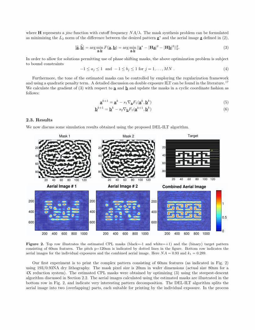
Figure 2. Top row illustrates the estimated CPL masks (black=-1 and white=+1) and the (binary) target patternconsisting of 60nm features. The pitch p=120nm is indicated by dotted lines in the figure. Bottom row indicates theaerial images for the individual exposures and the combined aerial image. Here NA = 0.93 and k1 = 0.289.
Our first experiment is to print the complex pattern consisting of 60nm features (as indicated in Fig. 2)using 193/0.93NA dry lithography. The mask pixel size is 20nm in wafer dimensions (actual size 80nm for a4X reduction system). The estimated CPL masks were obtained by optimizing (3) using the steepest-descentalgorithm discussed in Section 2.2. The aerial images calculated using the estimated masks are illustrated in thebottom row in Fig. 2, and indicate very interesting pattern decomposition. The DEL-ILT algorithm splits theaerial image into two (overlapping) parts, each suitable for printing by the individual exposure. In the process

Mask # 1
20 40 60 80
10
20
30
40
50
60
Mask # 2
20 40 60 80
10
20
30
40
50
60
Target
20 40 60 80
10
20
30
40
50
60
Aerial Image # 1
200 400 600
100
200
300
400
Aerial Image # 2
200 400 600
100
200
300
400
Combined Aerial Image
200 400 600
100
200
300
400 0.2
0.4
0.6
0.8
1
Figure 3. Top row illustrates the estimated CPL masks and the target pattern consisting of 80:320 vertical gratinginterlaced with 80nm wide horizontal features. Bottom row indicates the aerial images for the individual exposures andthe combined aerial image. Here NA = 0.85 and k1 = 0.35.
it automatically resolves all the possible phase-conflicts. The combined aerial image has very good quality andclosely resembles the target pattern.
In the next experiment, our goal is to print the target illustrated in Fig. 3 consisting of 80:320 verticalgratings (thin lines in between large spaces). Here the pixel-size is 20nm, NA = 0.85, radiation wavelength =193nm with corresponding k1 = 0.35 for smallest pattern pitch. The target also consists of a 80nm horizontallysandwiched space thereby making whole layout a challenging patterning problem. The estimated CPL masksobtained using DEL-ILT along with their corresponding aerial images are illustrated in Fig. 3. We again observean unconventional pattern decomposition, but the combined aerial image has very good contrast. In particular,note that there is a very well-defined separation (dark-area) between the horizontal space and grating line-ends;something very challenging to obtain using conventional H-V decomposition.
In conclusion, the DEL-ILT framework leads to un-intuitive but highly effective pattern decompositions.Unlike the commonly employed paradigm of splitting the (binary) target pattern, DEL-ILT aims to decomposethe (gray-level) aerial image. We also note that mask design for DEL is an ill-posed problem. Therefore, thepattern decompositions illustrated in Fig. 2 and Fig. 3 are not necessarily unique. In general there may bemultiple ways of splitting the patterns for double exposure. The preferred decomposition can be arrived at usingthe regularization framework. For example, a critical requirement for DEL is the robustness to mask-alignmenterrors. The above can be incorporated as a regularization function in order to obtain DEL masks which are alsotolerant to misalignment. This forms an important direction of future research.
3. DEL USING CONTRAST ENHANCEMENT LAYER (CEL) FOR K1 < 0.25
We now move on to the case of k1 < 0.25 and discuss CEL as a potential technology enabler for the abovecase. Contrast enhancement layer (CEL) is a photo-bleachable film which is coated on top of the conventionalphoto-resist. It was studied in the 1980s in order to improve the sidewall angle of single exposure lithographyprocess.6, 10, 11, 15 The CEL film is initially unbleached with (ideally) zero or very low transmittance for smalldose values. As the incident dose increases, the film starts undergoing bleaching action and the transmittanceincreases. The bleaching rate is related to the incident energy. The transmittance of an ideal fully bleached CEL

film is equal to one. Thus, the film which was initially opaque to the exposure wavelength, becomes transparentupon exposure. When the aerial image is incident on the CEL, higher intensity regions bleach faster comparedto lower intensity ones. This non-linear transformation of the incident aerial image leads to a higher contrast ofthe dose received by the resist. During the exposure, the unbleached portion of the CEL will act as a portableconformable mask. Finally, we want to point out that our current model takes a simplified view and ignores thereflections from the substrate.
3.1. Modeling
The (non-ideal) bleaching behavior of the CEL is similar to a soft-threshold operation. Therefore, the CEL filmtransmittance T (Di) can be modeled as a sigmoid function as follows,
T (Di) = sig(Di, a, tc, c) =1
1 + e−acDi+atc
, (7)
where Di is the incident dose, parameter c is inversely related to the thickness, a is related to the slope of thetransition region, and tc is the threshold dose parameter of the sigmoid. Fig. 4 indicates the behavior of a typicalsigmoid function with a = 60, tc = 0.15, and varying values of c. As discussed earlier, the transmittance is lowfor small values of incident dose. As the input dose builds up, the film starts bleaching and its transmittanceincreases (T (Di) = 0.5 for Di = tc/c). Fig. 4 also indicates the effect of the film thickness c on the filmtransmittance. A thin CEL film bleaches quickly compared to a thicker one, and hence has a steeper transitionregion. Furthermore, a thick CEL film also requires higher dose values to become fully transmissive.
0 0.2 0.4 0.6 0.80
0.2
0.4
0.6
0.8
1
Di
T(D
i)
c = 1c = 0.75c = 0.5c = 0.3
Figure 4. CEL film transmittance for different filmthickness.
0 0.2 0.4 0.6 0.80
0.1
0.2
0.3
0.4
0.5
0.6
0.7
Di
Dt
c=1c=0.75c=0.5c=0.3
Figure 5. Transmitted dose (Dt) versus input doseDi for different film thickness.
The final transmitted dose Dt{Di} (henceforth referred to as simply Dt), is obtained by integrating thetransmittance as the incident dose builds up from 0 to Di.
Dt =
∫ Di
0
T (Di)dDi =
∫ Di
0
1
1 + e−acDi+atc
dDi
Therefore,
Dt = Di −tcc
+1
aclog
[1 + e(−acDi+atc)
](8)
Fig. 5 indicates that the graph of transmitted dose versus incident dose consists of three regions. For lowdoses (unbleached film), the incident dose is absorbed by the CEL film and Dt is very low. When Di increases,the film starts bleaching and there is a non-linear increase in the transmitted energy. Finally, the CEL film getsfully bleached after which the transmitted dose increases linearly. As one would expect, the above regions alsodepend on the thickness of the CEL film. Thinner CEL films enter the linear region earlier compared to thethicker ones.

3.2. Working of CEL
We now discuss the working of CEL for the simple example of 1-D gratings. The target consists of 80nm (1:1)grating which needs to be printed using 193/0.85NA (kpitch = 0.35). The first step is to divide the target into two160nm pitch gratings which can be printed using single exposure CPL masks (with pitch = 320nm). Note thatthe second exposure consists of simply shifting the mask by 80nm. The leftmost plot in Fig. 6 indicates the aerialimage and the transmitted CEL image (calculated using (8)), both for the first exposure. The CEL transmitteddose is absorbed by the photoresist and stored in the form of PAC (photo-active compound) concentration.The center plot indicates the aerial image and the CEL dose for the second exposure. It is very important tohighlight here that in order to support DEL, the CEL considered should have reversible bleaching property. Inother words after the first exposure is completed, the entire CEL film returns back to its original (opaque) state.If the CEL were not reversible, the regions previously exposed would remain bleached and as such have differenttransmittance values than those indicated in Fig. 4. Development of the above material is central to the use ofCEL for double exposure. Such materials are not just hypothetical as is evidenced by class of reversible CEL(Arsel TM) under development by Pixelligent Inc.
The total dose absorbed by the resist is a superposition of the two CEL transmitted doses. The rightmostgraph in Fig. 6 indicates that the combined transmitted CEL dose (assuming the reversibility property) showsgood modulation. An intuitive explanation is that the CEL suppresses the aerial image energy in the unwantedregions owing to the soft-thresholding action. This has the effect of truncating the tail of the optical PSF (makingit narrower), and resulting in less energy being deposited in the areas targeted by the second exposure. Fig. 6also indicates the aerial image in the absence of CEL layer (just for demonstration purpose). Since kpitch < 0.5,no useful modulation is observed.
0 100 200 300 4000
0.2
0.4
0.6
0.8
1
x
Dt
0 100 200 300 4000
0.2
0.4
0.6
0.8
1
x
Dt
0 100 200 300 4000
0.2
0.4
0.6
0.8
1
x
Dt
Figure 6. The left and center figures indicate the aerial images and the CEL images for the two individual exposures. Thefigure on the right indicates the combined aerial image (showing no modulation) and the combined CEL image (showinggood modulation). In this case a = 30, tc = 0.15, and c = 0.45.
The image log-slope (ILS) calculated at the desired edge location (CD = 40nm) for the incoming aerial image(Di) and the CEL image (Dt) are 0.016 and 0.032 respectively. Thus the CEL also improves the aerial imagecontrast which was indeed one of the earliest applications of CEL.14 Finally, we also observe that the transmittedCEL doses have lower magnitude compared to the incoming (aerial image) dose. We discuss this in more detailin the next section.
4. IMPROVING ILS OF THE CEL IMAGE
Our goal now is to improve the robustness of the double exposure CEL-based lithography system. This will alsoenable us to understand the fundamental trade-offs involved in designing a CEL-DEL system. We have identifiedthree potential ways to improve the operating ILS at the desired edge location which are discussed below. Theexperimental setup employed here is the same as in Section 3.
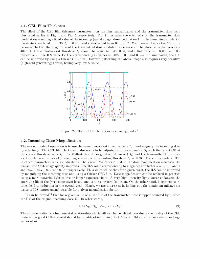
4.1. CEL Film Thickness
The effect of the CEL film thickness parameter c on the film transmittance and the transmitted dose wereillustrated earlier in Fig. 4 and Fig. 5 respectively. Fig. 7 illustrates the effect of c on the transmitted dosemodulation assuming a fixed value of the incoming (aerial image) dose modulation Di. The remaining simulationparameters are fixed (a = 30, tc = 0.15), and c was varied from 0.8 to 0.2. We observe that as the CEL filmbecomes thicker, the magnitude of the transmitted dose modulation decreases. Therefore, in order to obtain40nm CD, the photo-resist threshold tr should be equal to 0.48, 0.36, and 0.076 for c = 0.8, 0.5, and 0.2respectively. The ILS value for the corresponding tr values is 0.022, 0.03, and 0.054. To summarize, the ILScan be improved by using a thicker CEL film. However, patterning the above image also requires very sensitive(high-acid generating) resists, having very low tr value.
0 100 200 300 4000
0.2
0.4
0.6
0.8
1
x
Dose
c=0.8
c=0.5c=0.2
tr=0.076
tr=0.36
tr=0.48
Figure 7. Effect of CEL film thickness assuming fixed Di.
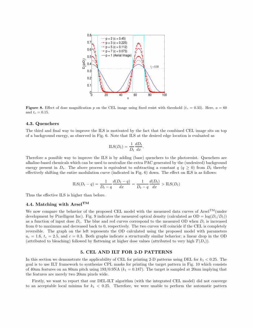
4.2. Incoming Dose Magnification
The second mode of operation is to use the same photoresist (fixed value of tr), and magnify the incoming doseby a factor p. The CEL film thickness c also needs to be adjusted in order to match Dt with the target CD atthe chosen threshold value tr. Fig. 8 illustrates the original aerial image (Di) and the transmitted CEL dosesfor four different values of p assuming a resist with operating threshold tr = 0.33. The corresponding CELthickness parameters are also indicated in the legend. We observe that as the dose magnification increases, thetransmitted CEL image quality improves. The ILS value corresponding to magnification factor k = 2, 3, 5, and 7are 0.032, 0.047, 0.072, and 0.087 respectively. Thus we conclude that for a given resist, the ILS can be improvedby magnifying the incoming dose and using a thicker CEL film. Dose magnification can be realized in practiceusing a more powerful light source or longer exposure times. A very high intensity light source endangers theoperating life of the (very expensive) lenses, and is a less preferable option. On the other hand, longer exposuretimes lead to reduction in the overall yield. Hence, we are interested in finding out the maximum mileage (interms of ILS improvement) possible for a given magnification factor.
It can be proved16 that for a given value of p, the ILS of the transmitted dose is upper-bounded by p timesthe ILS of the original incoming dose Di. In other words,
ILS(Dt(pDi)) <= p ∗ ILS(Di) (9)
The above equation is a fundamental relationship which will also be beneficial to evaluate the quality of the CELmaterial. A good CEL material should be capable of improving the ILS by a full-factor p (particularly for largevalues of p).
0 20 40 60 80 1000
0.1
0.2
0.3
0.4
0.5
0.6
0.7
0.8
x
Dt(p
Di)
p = 2 (c = 0.45)p = 3 (c = 0.225)p = 5 (c = 0.112)p = 7 (c = 0.073)p = 1 (Aerial Image)
tr = 0.33
Figure 8. Effect of dose magnification p on the CEL image using fixed resist with threshold (tr = 0.33). Here, a = 60and tc = 0.15.
4.3. Quenchers
The third and final way to improve the ILS is motivated by the fact that the combined CEL image sits on topof a background energy, as observed in Fig. 6. Note that ILS at the desired edge location is evaluated as
ILS(Dt) =1
Dt
dDt
dx.
Therefore a possible way to improve the ILS is by adding (base) quenchers to the photoresist. Quenchers arealkaline-based chemicals which can be used to neutralize the extra PAC generated by the (undesired) backgroundenergy present in Dt. The above process is equivalent to subtracting a constant q (q ≥ 0) from Dt therebyeffectively shifting the entire modulation curve (indicated in Fig. 6) down. The effect on ILS is as follows:
ILS(Dt − q) =1
Dt − q
d(Dt − q)
dx=
1
Dt − q
d(Dt)
dx> ILS(Dt)
Thus the effective ILS is higher than before.
4.4. Matching with ArselTM
We now compare the behavior of the proposed CEL model with the measured data curves of ArselTM(underdevelopment by Pixelligent Inc). Fig. 9 indicates the measured optical density (calculated as OD = log(Di/Dt))as a function of input dose Di. The blue and red curves correspond to the measured OD when Di is increasedfrom 0 to maximum and decreased back to 0, respectively. The two curves will coincide if the CEL is completelyreversible. The graph on the left represents the OD calculated using the proposed model with parametersac = 1.6, tc = 2.5, and c = 0.3. Both graphs indicate a structurally similar behavior; a linear drop in the OD(attributed to bleaching) followed by flattening at higher dose values (attributed to very high T (Di)).
5. CEL AND ILT FOR 2-D PATTERNS
In this section we demonstrate the applicability of CEL for printing 2-D patterns using DEL for k1 < 0.25. Thegoal is to use ILT framework to synthesize CPL masks for printing the target pattern in Fig. 10 which consistsof 40nm features on an 80nm pitch using 193/0.9NA (k1 = 0.187). The target is sampled at 20nm implying thatthe features are merely two 20nm pixels wide.
Firstly, we want to report that our DEL-ILT algorithm (with the integrated CEL model) did not convergeto an acceptable local minima for k1 < 0.25. Therefore, we were unable to perform the automatic pattern

Figure 9. OD versus Di for the proposed model (left) and the measured data using Arsel TM(right).
decomposition similar to one illustrated in Section 2. We suspect that this may be due to the local gradient-based search technique used for optimization. The algorithm is unable to explore the more complicated searchspace resulting from k1 < 0.25, and better initialization points may help solve the problem. However, thisremains a direction of future work.
10 20 30 40
10
20
30
40
50
60
70
10 20 30 40
10
20
30
40
50
60
70
10 20 30 40
10
20
30
40
50
60
70
Figure 10. The target pattern consisting of 40nm features on 80 nm pitch and the (manually) decomposed patterns usedfor individual exposures.
We therefore perform a rule-based pattern decomposition as illustrated in Fig. 10 and employ the singleexposure based ILT algorithm to synthesize the CPL masks. The augmented forward model also accounting forthe CEL is as follows:
z = F (G(p|Hm|2)), (10)
where the function G(.) represents the CEL transmittance function defined in (8). F (.) is a sigmoid functionwhich models the thresholding operation performed by the resist,20
F (y) = sig(y) =1
1 + exp(−ary + artr).
Here ar and tr are the slope and threshold parameters of the resist respectively. Thus the forward model in (10)accounts for the magnified incoming aerial image dose, the CEL transferred dose, as well as the resist contourformation. The estimated mask m is defined as one which minimizes the L2 norm of the difference between thetarget contour z∗ and output contour z modeled using (10),
m = arg minm
C1(m) = arg minm
||z∗ − z||22. (11)
The cost function in (11) is still continuous allowing the use of non-linear programming techniques for optimiza-tion. We follow our earlier proposed approach,20 and employ the gradient-descent optimization algorithm to

minimize C1(m). The gradient can be calculated as follows:
∇C1(m) = −4arpHT[(z∗ − z) � z � (1− z) � (Hm) � q], (12)
where
q =1
1 + exp(−accp|Hm|2 + actc).
Fig. 11 illustrates the results obtained using the CEL-ILT algorithm discussed above. The top row indicatesthe estimated CPL mask (white = 1 and black = -1), the aerial image, and the CEL image for a single exposure.The simulations parameters were: ac = 60, tc = 0.15, c = 0.2, p = 4, ar = 60, tr = 0.3. We observe that althoughthe aerial image is very poor, the CEL transmitted image (Dt) has much better contrast, and closely resemblesthe target. This is because our ILT algorithm is aware of the presence of CEL, and estimates the masks takingits action into account. By the end of the first exposure, the CEL transmitted dose is completely absorbed by thephotoresist, where it is stored in the form of PAC concentration. The second exposure is performed by simplyshifting the mask horizontally by 320nm (see Fig. 10). The bottom row in Fig. 11 indicates that the combinedaerial image (the dose received by the resist in the absence of CEL) has no useful modulation. This is expectedbecause kpitch < 0.5. However, the linear superposition of the two CEL images shows very good modulation,which will enable patterning of the desired features. The contours at tr = 0.3 indeed indicate good patternfidelity.
Mask
10 20 30 40
10
20
30
40
50
60
70
−1
−0.5
0
0.5
1Aerial Image (Single Exposure)
100 200 300
100
200
300
400
500
600 0
0.5
1
1.5
CEL Image (Single Exp)
100 200 300
100
200
300
400
500
600
0.1
0.2
0.3
0.4
0.5
0.6
0.7
0.8
Combined Aerial Image
100 200 300
100
200
300
400
500
6000.2
0.4
0.6
0.8
1
1.2
1.4
1.6
1.8
Combined CEL Image
100 200 300
100
200
300
400
500
600
0.1
0.2
0.3
0.4
0.5
0.6
0.7
0.8
Contour (tr=0.3)
100 200 300
100
200
300
400
500
600 0
0.2
0.4
0.6
0.8
1
Figure 11. The top row indicates the CEL-ILT results obtained by solving (11). The bottom row indicates the DELresults where the second exposure was performed by shifting the mask by 240nm.
6. TWO-PHOTON ABSORPTION RESIST
The second OSOM material candidate for k1 < 0.25 DEL is two-photon absorption resist. They have beenwell-known to double the resolution of optical lithography, and were actively explored by Yablonovitch, et al.24

0 2 4 6 80
0.5
1
1.5
2
x
y
y = 1 + cos(K x )
0 5 100
1
2
3
4
x
y
y = 3 /2 + 2 cos(K x ) + 1/2 cos(2 K x )
Figure 12. The intensity and square of intensity modulation curves corresponding to the conventional and 2-photonabsorption resists respectively.
The left graph in Fig. 12 illustrates the aerial image intensity obtained using an interferometric arrangementwith 2-coherent beams incident at ±θ. Therefore, I(x) = 1 + cos(Kx) where K = 2k sin θ. For the case of two-photon absorption, the resist responds to the square of the intensity. Thus I2(x) = 3/2+2 cos(Kx)+1/2cos2Kx,which consists of superposition of both the single and double-frequency components. As observed in Fig. 12, theabove mixture merely enables patterning at the same resolution as single-photon absorption (although with abetter contrast). Therefore, we need to get rid of the linear frequency component in order to enable frequencydoubling, and allow kpitch < 0.5. Yablonovitch, et al24 proposed a new (single) exposure arrangement whichdestroys the stationary interference patterns corresponding to the linear frequency component, leaving behindthe double-frequency interference pattern on a background.
A alternative way to enable frequency doubling using 2-photon absorption resists is by employing DEL. Inthe case of gratings, the second exposure should have an offset of half a period compared to the first. Thereforethe combined contribution from the two exposures is given as follows:
I21 (x) + I2
2 (x) = [1 + cos(Kx)]2 + [1 + cos(Kx + π)]2
= [1 + 2 cos(Kx) + cos2(Kx)] + [1 − cos(Kx)]2
= [1 + 2 cos(Kx) + cos2(Kx)] + [1 − 2 cos(Kx) + cos2(Kx)]
= 2 + 2 cos2(Kx)
= 3 + cos(2Kx)
We observe that by merely shifting and adding I2(x), the linear frequency component cancels out, leavingbehind only the double-frequency component with a DC background. Thus 2-photon absorption resists arenaturally suitable to DEL. Yet, we are not aware of materials with suitably large 2-photon absorption cross-section value at wavelength of interest. As a result one would need very high power at the wafer plane to obtainsignificant two-photon excitation rates with existing materials, making it practically possible, but economicallyunsuitable for high volume manufacturing.
7. CONCLUSION AND FUTURE WORK
In this paper we discussed two different paradigms of double exposure single development lithography. Fork1 > 0.25, we discussed a new approach of using ILT to decompose the aerial image and simultaneously estimatingthe two masks best suited for the purpose. The combined aerial image has very good contrast and will enablepatterning close to k1 = 0.25. For the case of k1 < 0.25, we identified CEL and two-photon absorption resistsas two potential candidates. We presented the mathematical model of a desirable reversible CEL material(neglecting the reflections from the substrate) and discussed several ways of improving the aerial image slope. Acomparison with ArselTM(by Pixelligent Inc.) provided encouraging results. Reversibility of the CEL film wasidentified as the key enabler for the success of DEL. We also presented simulation results for patterning 1-D and2-D features using a combination of CEL, DEL, and ILT. For two-photon absorption resist, the biggest challengeis the unavailability of a material with necessarily high cross-section for 2-photon absorption.
The proposed CEL model assumes 100% opacity and 100% transparency for unbleached and fully bleachedstates respectively, which is impractical. The future work consists of refining the CEL model to incorporate thepractical transmittance values of the CEL film. We also hope to carry out physical experiments using CEL andreport the results in our future publications.
REFERENCES
1. A. Biswas, J. Li, J. Hiserote, and L. Melvin III, Extension of 193nm dry lithography to 45-nm half-pitchnode: Double exposure and double processing technique, BACUS Symposium on Photomask Technology,Proc. SPIE, vol. 6349, 2006.
2. T. Chiou, A. Chen, S. Hsu, M. Eurlings, and E. Hendrick, Development of automatic OPC treatment andlayout decomposition for double dipole lithography for low-k1 imaging, Advanced Microlithography Tech-nologies, Proc. SPIE, vol. 5645, 2005, pp. 21–31.
3. A. Erdmann, R. Farkas, T. Fuhner, B. Tollkuhn, and G. Kokai, Towards automatic mask and source opti-mization for optical lithography, Optical Microlithography, Proc. SPIE, vol. 5377, 2004, pp. 646–657.
4. J. Park et al, Application challenges with double patterning technology beyond 45nm, BACUS Symposiumon Photomask Technology, Proc. SPIE, vol. 6349, 2006.
5. M. Fritze, B. Tyrrell, D. Astolfi, R. Lambert, D. Yost, A. Forte, S. Cann, and B. Wheeler, Subwavelengthoptical lithography with phase-shift-mask, Lincoln Laboratory Journal 14 (2003), 237–250.
6. L.F. Halle, A water soluble contrast enhancement layer, Journal of Vaccuum Science and Technology B 3(1985), 323–326.
7. M. Hasegawa, A. Suzuki, K. Saitoh, and M. Yoshii, New approach for realizing k1 = 0.3 optical lithography,Symposium on Photomask and X-Ray Mask Technology, Proc. SPIE, vol. 3748, 1999, pp. 278–287.
8. S. Hsu, J. Park, D. Broeke, and J. Chen, Double exposure technique for 45nm and beyond, BACUS Sympo-sium on Photomask Technology, Proc. SPIE, vol. 5992, 2005.
9. Y. Liu and A. Zakhor, Optimal binary image design for optical lithography, Optical Microlithography, Proc.SPIE, vol. 1264, 1990, pp. 401–412.
10. W. Loong and H. Pan, A direct approach to the modeling of polydihexisilane as a contrast enhancementmaterial, Journal of Vaccuum Science and Technology B 8 (1990).
11. C. Mack, Contrast enhancement techniques for submicron optical lithography, Journal of Vaccuum Scienceand Technology A 5 (1987).
12. C. Noelscher, M. Heller, B. Habets, M. Markert, U. Scheler, and P. Moll, Double line shrink lithography atk1 = 0.16, Microelectronic Engineering 83 (2006), 730–733.
13. Y. Oh, J. C. Lee, and S. Lim, Resolution enhancement through optical proximity correction and stepperparameter optimization for 0.12-µ mask pattern, Optical Microlithography, Proc. SPIE, vol. 3679, 1999,pp. 607–613.
14. W. Oldham, The use of contrast enhancement layers to improve the effective contrast of positive photoresist,IEEE Transactions on Electron Devices 34 (1987), 247–251.
15. E. Ong, B. Singh, R. Ferguson, and A. Neureuther, Comparison of proximity effects in contrast enhancementlayer and bilayer resist processes, Journal of Vaccuum Science and Technology B 5 (1987), 443–448.
16. A. Poonawala, Single and double exposure inverse lithography mask design for optical lithography (in prepa-ration), Ph.D. thesis, University of California, Santa Cruz, 2007.
17. A. Poonawala and P. Milanfar, Double exposure mask synthesis using inverse lithography, Submitted toJournal of Microlithography, Microfabrication and Microsystems (Preprint available online).
18. , Prewarping techniques in imaging: Applications in nanotechnology and biotechnology, ElectronicImaging, Proc. SPIE, vol. 5674, 2005, pp. 114–127.
19. , OPC and PSM design using inverse lithography: A non-linear optimization approach, OpticalMicrolithography, Proc. SPIE, vol. 6154, 2006, pp. 114–127.
20. , Fast and low-complexity mask design in optical microlithography - an inverse imaging problem, Toappear for Publication in IEEE Transactions on Image Processing (2007).
21. S. Sayegh and B. Saleh, Image design: Generation of a prescribed image at the output of a bandlimitedsystem, IEEE Transcation on Pattern Analysis and Machine Intelligence 5 (1983), 441–445.

22. S. Sayegh, B. Saleh, and K. Nashold, Image design: Generation of a prescribed image through a diffractionlimited system with high-contrast recording, IEEE Transaction on Acoustics, Speech and Signal Processing33 (1985), 460–465.
23. S. Sherif, B. Saleh, and R. Leone, Binary image synthesis using mixed linear integer programming, IEEETransactions on Image Processing 4 (1995), 1252–1257.
24. E. Yablonovitch and R. Vrijen, Optical projection lithography at half the rayleigh resolution limit by two-photon exposure, Optical Engineering 38 (1999), 334–338.


![2 LASER INTERFERENCE LITHOGRAPHY - uni-halle.de · 2 LASER INTERFERENCE LITHOGRAPHY (LIL) 9 2 LASER INTERFERENCE LITHOGRAPHY (LIL) Laser interference lithography [3~22] (LIL) is a](https://img.pdfslide.net/doc/110x75/5eae180eecc7e273a41a4e88/2-laser-interference-lithography-uni-hallede-2-laser-interference-lithography.jpg)