Embed Size (px)
Citation preview

20 SEMICONDUCTOR International � August 2009 www.semiconductor.net
The range of products whose fabrication depends on wafer-to-wafer bonding is growing rapidly, and includes MEMS, wafer-level packaging and various types of 3-D integration. The wafers them-selves may be made of silicon, com-
pound semiconductors, sapphire, glass, quartz or other materials. An emerging consumer market that uses wafer bonding is high-brightness light-emitting
diodes (HB-LEDs), which promise to achieve a level of efficiency and economy for general lighting that will make both incandescent and fluorescent light sources obsolete.
Several methods of wafer bonding have been developed for diverse applications. Manufacturers of MEMS devices use bonding methods to create a sealed protective cavity within which their miniatur-ized elements can operate. In MEMS and other areas where wafer bonding is used, the overall packaging operation, including the bonding of wafers, tends to be both expensive and time-consuming. Since the
wafer bonding processes occur at or near the end of the front-end-of-line processing, the wafers usu-ally contain fully functional devices worth many
hundreds of dollars. Yield loss is a critical parameter to monitor, and keeping the processes under con-trol by critical monitoring is essen-tial to cost-effective production.
Bond-interface defects affect the hermeticity, mechanical strength and potentially the electrical iso-lation of the upper and lower de-vice components. Flaws can occur at the wafer-wafer interface after bonding, including non-bonded areas and voids (a very thin vacuum or air bubble), typically caused by foreign particles, scratches or sur-face contamination. For example, in Cu-Cu bonding for 3-D inte-gration, the copper lines and pads that connect the two wafers can be corroded, leading to an imperfect
bond and loss of electrical contact between devices on the bonded wafer stack. A foreign particle be-tween two direct-bonded silicon wafers during the silicon-on-insulator (SOI) bond process will result in a characteristic non-bonded area surrounding the particle.
The preferred method of inspection for these flaws is acoustic micro-imaging, which is very sensi-tive to internal material interfaces. Infrared radia-tion can image the wafer pair, but is sensitive only to large flaws and IR-transparent materials. X-ray does not work well for polycrystalline interfaces. In
A practical, acoustic imaging technique is applied to bonded waferpairs to image interface defects and wafer scratches in various materials.
ImagingBonded Wafer Defects for 3-D
1. Reflection-mode acoustic image and waveforms of two direct-bonded silicon wafers. Voids produce high-amplitude echoes, while bonded areas produce no echo.
Direct-Bonded Silicon Wafers
“ In Cu-Cu bonding, the copper lines can be corroded, leading to
loss of electrical contact.”
six0908bondID 20six0908bondID 20 8/5/2009 12:26:00 PM8/5/2009 12:26:00 PM

21www.semiconductor.net August 2009 � SEMICONDUCTOR International
the examples cited above, the high-frequency ultra-sound of acoustic micro-imaging will image the cop-per pads during Cu-Cu bonding, and identify imper-fections within the copper lines, the non-bonded area in the Si-Si wafer pair, and the particles themselves.
Acoustic micro-imaging systems use a raster-scan-ning transducer that emits pulses of ultrasound into the bonded wafer pair and collects the return echoes. Pulses sent into the wafer pair are focused at the depth of interest, which is typically the bond interface loca-tion. The return echo is then converted into acoustic data and used to make acoustic images accepted only from a user-defined depth range. These acceptance windows of information are called gates. By moving the gate, the user can sample information from very narrow slices from the upper surface of the bonded stack, bond interface and from the bottom surface. Unwanted return echo signals not within the gate range are ignored.
Transducers used in imaging wafer pairs typically emit ultrahigh-frequency ultrasound at 230 MHz or higher. Echoes are returned only from material interfaces, and not from the bulk of ho-mogeneous materials. The percentage of the pulse that is reflected as a usable signal is deter-mined by the acoustic impedance (material density × acoustic ve-locity) between the two materials, and can be
determined by:
where R is the relative amplitude, and z
1 and z
2
are the acoustic imped-ance values of the two materials at the interface.
If a wafer pair consists of two direct-bonded silicon wafers, the two materials are identical and, assuming that there is no defect or anomaly at the bonded interface, there will be no reflection. The desired acoustic image of such a wafer pair is a featureless black image, because the amplitude of the returned echo is zero.
If the wafer pair consists of two different materials, the acoustic image will be featureless and brighter if there are no anomalies or defects. If there are streets
Shari Farrens and Sumant Sood,Wafer Bonder Division, SUSS MicroTec, www.suss.comRay Thomas, SonoLab manager, Sonoscan Inc., www.sonoscan.com
(z2-z
1)
R= (z
2+z
1)
3. A tiny particletrapped between BCB-bonded wafersresults in a much larger air gap.
4. Acoustic imageof the wafer at left shows missing (circle) and incomplete (arrow) for-mation of the ring seal. The image at right shows good glass frit seal rings.
2. C-SAM images of Au-Si bond interface for two bonded wafer stacks bonded at 405ºC (poor bond, left) and 390ºC (good eutectic bond, right).
Glass Frit Bonded Wafers
Eutectic (Au-Si) Bonded Wafers
six0908bondID 21six0908bondID 21 8/5/2009 12:26:10 PM8/5/2009 12:26:10 PM

22 SEMICONDUCTOR International � August 2009 www.semiconductor.net
of a third material such as copper or gold, the streets are visible, as are any defects. Such a bond pair has two material inter-faces rather than one. Specifically, there will be one interface between perfectly bonded areas that are non-reflective and a second interface between each substrate and the flaw.
The amplitude of the return echo sig-nal is vastly greater if the ultrasonic pulse encounters the interface between a solid and air, as occurs when there is a void (unbonded area) at the bond interface. Compared with any solid wafer materials, air has such a low acoustic velocity (343 m/sec) and density (0.00129 g/cm3) that application of the above formula invariably results in a reflection amplitude >99.99%. An unbonded area, an air pocket around a defect or particle, a crack, or any other gap-type feature will thus be imaged much more brightly than bonded areas.
Direct-bonded wafer pairsAvoiding bond interface particles is critically important in Si-Si wafer bonding, a key step in the manufacture of SOI wafers as well as for some MEMS devices that are packaged via direct bond-ing processes. Figure 1 shows the acoustic image of the bond zone between two direct-bonded sili-con wafers and waveforms for the three locations noted. The image shows an unbonded area (white) as well as well-bonded areas (black). The waveforms show a center region that is bracketed by two vertical lines, which define the gate used to create the image. As the transducer scans across the wafer, various interface con-ditions are sampled. The wave-forms labeled 1, 2 and 3 show the signal response within the gate region corresponding to the wafer locations identified in the image. In location 1 there is no signal reflection within the gated region. The waveform does indicate strong signals from the front and back surfaces to the left and right, respectively, of the two vertical lines. The bond is good.
The interface void at location 2 is completely white, which corresponds to a large air gap, and the signal output is also well defined. Particularly at wafer edges, anomalous features may oc-cur due to material handling touch points, abrasion from cassettes or chemical residues. In location 3, part of the image appears gray and may represent the ingression of water into a void or debond that is open to the exterior. The void in this case contains a substance with a different density than air but is not bonded.
Hence, the signal amplitude, as indicated by the waveform, shows intermediate signal strength between the void and the well-bonded regions.
Metal/eutectic-bonded wafersMetal materials, when joined with high temperature and high force, form a diffu-sion bond. Another class of metal bonds includes eutectic alloys such as Au-Sn, Au-Si, Cu-Sn or Au-In, which can be used to create self-planarizing interfaces or to re-duce processing temperatures to <400ºC.
The most important feature of all metal bonding technologies is the increased hermeticity and the corresponding ability to reduce sealing geometries and device size as a direct result.
The integrity of metal and eutectic bonds can be determined by focusing and gating the acoustic image at the interface between the wafer and the bonding material. When analyzing MEMS bonds it is helpful to visualize the sealed cavity area as a geo-metrically defined void. Thus the cavity areas will appear very bright. Figure 2 shows Au-Si bond interfaces for two bonded wa-
fer stacks. In the first image, the bonded wafer pair was subjected to higher bond temperature (405ºC) while the pair in the sec-ond image was bonded at 390ºC. Since the eutectic temperature for a Au-Si bond is 363ºC, the result is uncontrolled eutectic flow into seal rings in some areas of the wafers in the first image but a controlled eutectic reaction and perfect bonds around cavities at the lower temperature.
Adhesive-bonded wafersAdhesive films such as benzocy-clobutene (BCB) are also used as a bond interface for 3-D integra-tion. Voids in such bond types are attributed to surface defects, to-pography and thermomechanical stresses during bonding. Polymers such as BCB and polyimides have relatively low acoustic imped-
ances. As a result, a gap-type defect such as a void may be more difficult to distinguish from nearby well-bonded regions due to small variances in the signal amplitude. During C-mode scan-ning acoustic microscopy (C-SAM) analysis, it is often helpful to reduce time of flight (TOF) by moving the transducer closer to the top surface of the wafer pair to obtain optimal focus at the bonded interface.
Figure 3 shows a C-SAM image of 200 mm wafers bonded using BCB. The inset expands the region of interest around the air pocket surrounding a foreign particle lodged between the two wafers. Foreign particles typically cause mild doming of the wa-
Imaging Bonded Wafer Defects for 3-D
5. Acoustic image of a crack at the bond interface in an Au-Si bonded wafer pair.
“ The most important feature of all metal bonding
technologies is the increased hermeticity and the
corresponding ability to reduce sealing geometries
and device size.”
six0908bondID 22six0908bondID 22 8/5/2009 12:26:22 PM8/5/2009 12:26:22 PM
23www.semiconductor.net August 2009 � SEMICONDUCTOR International
fers, and the surrounding air pocket is often circular. The contrast between the air pocket and the surrounding defect-free areas is adequate for diagnosis, but less pronounced than it would be with a different bonding method.
Glass frit wafer bondingGlass-frit bonding has been used for wafer-level packaging of MEMS devices for more than a decade. Since the bonding material provides hermetic protection for the de-vice, the echoes are gated on the bond seal-ing surfaces to examine the interface. In the acoustic image of the bond interface, the device cavities are expected to appear bright while the bond material (glass frit) will appear darker. In the first wafer pair in Figure 4, part of the glass frit seal is missing (circle) from several devices. In other areas (arrows), the width of the frit seal is vari-able, perhaps as the result of problems during screen printing. In the wafer pair in the second image, the frit mesh has no defects.
Cracks in bonded wafersCracks in bonded wafers can be very difficult to detect optically and can be challenging to image acoustically because they are of-ten nearly vertical in orientation. Sonoscan developed a technique that simplifies the imaging of cracks by using the reflection of the pulsed ultrasound from the bond interface to create an acoustic shadow of the crack. With this method, the size of the crack is proportional to the depth of the crack, making it more visible to the sensor and variations in depth along a crack can be detected.
Figure 5, the shadow-method acoustic image of a crack at the bond interface in an Au-Si bonded wafer pair, could not be de-tected or imaged by other methods.
Frequency domain imagingThe previous acoustic images were all made with the acoustic mi-cro-imaging method called time-domain imaging (TDI), meaning that the image is defined by a depth selected by the round-trip travel time of the sound wave. In bonded wafer applications where it is important to achieve high resolution and high contrast, a sec-ond method called frequency domain imaging (FDI) is often used.
FDI use s a pulse of ultrasound launched by a 230 MHz transducer to produce fre-
quencies on both sides of the nominal frequency of 170-260 MHz, for example. FDI decomposes the return echoes into individual frequencies to generate 20-30 images, each with a corresponding frequency. The advantage of FDI is that a given interface generally reflects different frequencies in very different ways. Thus a feature at an interface that is hardly visible at one frequency, or in TDI,
may be easily visible at a different FDI frequency.
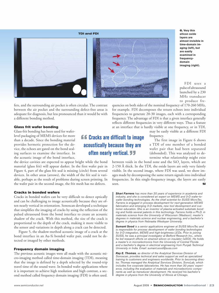
The first image in Figure 6 shows a TDI of one member of a bonded wafer pair that had been separated (debonded). This was analyzed to de-termine what relationship might exist
between voids in the bond zone and the SiO2 layers, which are
2-150 Å thick. In the TDI, the oxide layers are only very faintly visible. In the second image, where FDI was used, we show im-ages made by decomposing the same return signals into individual frequencies. In this single-frequency image, the layers are easily seen. SI
6. Very thin silicon oxidelayers are almost invisible in time-domain im-aging (left), but are easily examined in frequency-domain imaging (right).
Shari Farrens has more than 20 years of experience in academia and industry, and she is considered an expert on MEMS and 3-D wafer-to-wafer bonding technologies. As the chief scientist for SUSS MicroTec, Farrens is engaged in process development for next-generation MEMS fabrication and emerging 3-D markets, new tool development and cus-tomer education. She is an inventor of plasma-activated substrate bond-ing and holds several patents in this technology. Farrens holds a Ph.D. in materials science from the University of Wisconsin (Madison), master’s degrees in materials science and nuclear engineering, and a bachelor’s degree in physics from Nebraska Wesleyan University.
Sumant Sood is a senior applications engineer at SUSS MicroTec and is responsible for process development of wafer bonding technologies for 3-D integration, MEMS and high-brightness LEDs. Prior to joining SUSS, he was a principal investigator at Belford Research Inc., where he led research efforts on strained silicon on insulator (sSOI). He holds a master’s in microelectronics from the University of Central Florida and a bachelor’s degree in electrical engineering from Punjab Technical University in India. Email: [email protected]
Ray E. Thomas, as director of the Analytical Services Division of Sonoscan, provides technical and sales support as well as specialized training to customers and engineers worldwide. Prior to becoming direc-tor, Thomas managed the Analytical Services Division, SonoLab, which includes five corporate laboratories. He has more than 30 years’ experi-ence, including the evaluation of materials and microelectronic compo-nents as well as transducer development. He received his bachelor’s degree in physics from the University of Illinois at Chicago.
TDI and FDI
“ Cracks are difficult to image acoustically because they are
often nearly vertical.”
six0908bondID 23six0908bondID 23 8/5/2009 12:26:33 PM8/5/2009 12:26:33 PM


![PMMA-Based Wafer-Bonded Capacitive Micromachined ... · Transducers for underwater acoustic applications are designed to operate in the 100 kHz–2 MHz frequency range [32]. The transducer,](https://img.pdfslide.net/doc/110x75/600691a7b312da08161bd453/pmma-based-wafer-bonded-capacitive-micromachined-transducers-for-underwater.jpg)


![Intelligent Fault Diagnosis System for Radiographic Images …...A variety of automated defect detection and classification systems have been applied extensively to wafer defects [7,8]](https://img.pdfslide.net/doc/110x75/61163cc7be4a1d113728b89f/intelligent-fault-diagnosis-system-for-radiographic-images-a-variety-of-automated.jpg)