Embed Size (px)
Citation preview
Research Article Vol. 28, No. 10 / 11 May 2020 / Optics Express 14536
Imaging of surface plasmon polaritons inlow-loss highly metallic titanium nitride thinfilms in visible and infrared regimes
MENA N. GADALLA,* KUNDAN CHAUDHARY, CHRISTINE M.ZGRABIK, FEDERICO CAPASSO, AND EVELYN L. HU
John A. Paulson School of Engineering and Applied Sciences, Harvard University, Cambridge,Massachusetts 02138, USA*[email protected]
Abstract: Titanium nitride (TiN) has been identified as a promising refractory material for hightemperature plasmonic applications such as surface plasmon polaritons (SPPs) waveguides, lasersand light sources, and near field optics. Such SPPs are sensitive not only to the highly metallicnature of the TiN, but also to its low loss. We have formed highly metallic, low-loss TiN thin filmson MgO substrates to create SPPs with resonances between 775-825 nm. Scanning near-fieldoptical microscopy (SNOM) allowed imaging of the SPP fringes, the accurate determination ofthe effective wavelength of the SPP modes, and propagation lengths greater than 10 microns.Further, we show the engineering of the band structure of the plasmonic modes in TiN in themid-IR regime and experimentally demonstrate, for the first time, the ability of TiN to supportSpoof Surface Plasmon Polaritons in the mid-IR (6 microns wavelength).
1. Introduction
Recently, there has been growing interest in the exploration of refractory plasmonic materials,which can demonstrate superior behavior at elevated temperatures and powers, compared tothe more commonly used gold and silver [1,2]. TiN has demonstrated its capabilities as sucha refractory material, and several studies have demonstrated thin films of highly metallic TiN,with large negative values of the real part of the material permittivity [Re (ε)] using differentdeposition techniques such as magnetron sputtering [1,3–7], nitrogen-plasma-assisted molecular-beam epitaxy [8], and pulsed laser deposition [9]. In this paper we optimize the formation ofTiN thin films on MgO to achieve both large negative values of Re (ε), as well as small valuesof Im (ε). Such TiN films are ideally suited to demonstrate surface plasmon polariton (SPP)resonances with long propagation lengths. Surface Plasmon Polaritons (SPPs) are coupledstates between photons and plasma oscillations that are localized along the interface between aplasmonic material and a dielectric. Currently, SPPs with long surface propagation distances arebeing considered as the basis of interconnects [10,11], enabling photonic information processing.The robustness of SPP resonances and propagation lengths is sensitive to both the highly metallicnature of the plasmonic material and to its low loss. The high quality of our TiN thin films isdemonstrated in the SPP resonances supported in the 775-825 nm wavelength range. Moreover,we are able to directly image the SPP fringes using SNOM. This near-field assessment allows usto determine the effective wavelengths of the SPP modes, and to measure propagation lengthsgreater than 10 microns. We are able to extend SPPs to much longer wavelengths (6 microns)through the creation of Spoof SPPs by patterning the TiN to alter its dispersion characteristics.To guide and calibrate our studies, we carried out a full simulation of the Air/TiN/MgO structuresused to model and understand the dispersion relations of the plasmon modes. In aggregate, webelieve that the highly metallic and low loss properties of our TiN plasmonic films extend therange of SPP-enabled sensing and communications to higher temperatures made possible byrefractory TiN.
#391482 https://doi.org/10.1364/OE.391482Journal © 2020 Received 27 Feb 2020; revised 1 Apr 2020; accepted 2 Apr 2020; published 28 Apr 2020

Research Article Vol. 28, No. 10 / 11 May 2020 / Optics Express 14537
2. Low loss TiN thin film deposition and dispersion analysis
Highly metallic TiN thin films were reactively sputtered onto <100>MgO substrates at asubstrate temperature of 700 °C, 200V applied substrate bias, and with the ratio of argon tonitrogen equal to 12:4 sccm. The deposition pressure was held at 4 mT with base pressure of thesputtering chamber of around 5 × 10⁻⁸ Torr. These conditions were optimized to improve theplasmonic properties of the TiN film by maximizing negative Re (ε) while keeping the lossesas low as possible by minimizing Im (ε). As was done in Refs. [12,13], we can extract thefrequency dependent optical properties of the resulting film using Ellipsometric measurementstaken with Woollam WVASE32 vertical angle spectroscopic rotating-analyzer. Measurementswere taken at three different incidence angles: 55°, 65°, and 75°. The Drude-Lorentz [14,15]model was then used to fit the data. Similar to the model presented in [5], our model consistsof a Drude oscillator (damping (ΓD)= 0.3 and plasma frequency (ωp)= 6.5) representing thefree d-band conduction electrons [16], two Lorentz oscillators representing the inter-band losses(energy (ω0)= 4.35 and 2.52, damping (γ)= 1.48 and 1.14, oscillator strength (ω2
l )= 37.6 and2.6 respectively), and a background offset (ε∞) of 4.16 representing the high energy inter-bandtransitions. More details about the sputtering process, stoichiometry, chemical composition,and carrier concentrations of our TiN films can be found in our previous publications [1,7,12].Figure 1(a) compares the real and imaginary part of the measured dielectric function of our TiN tothat of Au using values from Ref. [17]. Our TiN thin film exhibits both strong metallic behaviorwith high negative Re (ε) values, close to that of Au, as well as very low losses, manifested inthe low values of Im (ε). In order to understand SPP coupling in our structures, we study thedispersion relation of the plasmon modes at the interface between TiN and air as well as TiN andMgO at different frequency regimes. For thin metallic films (40 nm TiN in our case), cross talkbetween the plasmonic modes across both interfaces (Air/TiN and TiN/MgO) is possible. At650 nm, the evanescent decay length (confinement length normal to the surface) within the TiNcan be calculated as (2|k1 |)−1 where k1is the attenuation constant in TiN and is given by Eq. (1)with i= 1. For the modes excited at the MgO and air interfaces, this decay length is 30 nm and35 nm respectively. These values increase at longer wavelengths. Therefore, for such a multilayersystem, the TM modes in the core of the TiN are a superposition of two plane waves with thesame propagation constant (the wave vector kx is continuous across the thickness of the TiNwith the same value at both interfaces) but with different attenuation constants in+ z and –z,representing the superposition of the upper SPPs modes (Air/TiN interface) and the lower SPPsmodes (TiN/MgO interface). Enforcing continuous solutions that satisfy the wave equation leadsto four non-linear equations that represent the dispersion relation for a multilayer system [Eq. (1)with i= 1, 2, and 3, and Eq. (2)] [18]:
k2i = k2x − k20εi (i = 1, 2, 3) (1)
e−4k1a =k1ε1+
k2ε2
k1ε1−
k2ε2
k1ε1+
k3ε3
k1ε1−
k3ε3
(2)
kx is the propagation constant of the SPPs at either interface of a thin filmwith thickness 2a. k1, k2,and k3 are the attenuation constants in TiN, MgO, and air respectively. k0 is the propagationconstant of the incident plane wave freely propagating mode in air that is used to couple to theSPPs, and is equal to ω
c0 where ω and c0 are the angular frequency and the free space velocity ofthe incident plane wave. Solving Eq. (1) (with i= 1, 2, and 3) and Eq. (2) results in multiplefrequencies (modes) for each value of the wave vector, kx. Figure 1(b) shows finite differencetime domain (FDTD) simulations of the plasmonic dispersion relation for our TiN multilayerinsulator-metal-insulator (IMI) system for the case of Air/TiN/MgO (excitation is initiated fromthe air side) and MgO/TiN/Air (excitation is initiated from MgO side). In addition, the dispersion

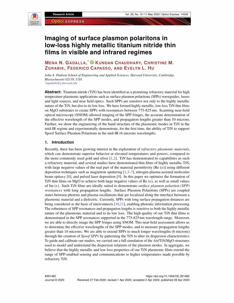
Research Article Vol. 28, No. 10 / 11 May 2020 / Optics Express 14538
relation of the SPPs on a single interface between two infinite mediums is overlaid as dottedwhite and black lines for the case of Air/TiN and MgO/TiN respectively. To obtain these graphs,Air/TiN/MgO were placed within the Lumerical FDTD simulation domain terminated with Blochboundary conditions (BCs). We place a cloud of dipoles with different phase and orientationwithin the simulation domain. We then sweep over different values of the wave vector kx andfor each value we find the frequencies at which strong electric field resonance is observed. It isworth mentioning here that the simulation time should be long enough to allow for completeattenuation of the modes that are not supported by the structure. The air light-line and theMgO light-line represent the dispersion relations of the free propagating plane wave in air andMgO, respectively. On the left of the air light-line lies the TiN bulk plasmon band. On theright of the light-line we see the dispersion relation of the SPPs in the case of the Air/TiN/MgOsystem centered on the Air/TiN single interface dispersion relation (dotted white line). At lowfrequencies, the SPP of the Air/TiN/MgO system is represented by a line that coincides with theair line, whereas at higher frequencies that line branches into a band of frequencies representingmultiple modes (different possible frequencies for the same value of the wave vector) centered onthe single interface SPP dispersion relation. This band is represented by the faded white areain Fig. 1(b) between the labels “high frequency odd modes” and “low frequency even modes.”The solutions with frequencies higher than the single interface SPPs exhibit odd vector parity
1
Fig. 1. (a) Real and Imaginary part of the dielectric function of Au and our sputtered TiN thin film on MgO substrate obtained by spectroscopic ellipsometry, showing the close resemblance between both Re (ε) and Im (ε) of our optimized TiN thin films and those of Au. (b) FDTD numerical simulations of the surface plasmon band diagram in IMI system with the dispersion relation of single interface overlaid as dotted white and black lines for the case of Air/TiN and MgO/TiN respectively. This plot was obtained using FDTD simulations by sweeping over the wave vector to find corresponding frequencies at which the coupled electric field is maximized. The change in color along the SPP trace reflects the strength of the resonance at each point. For small wave vectors (dark red color), each wave vector has strong coupling at a single corresponding frequency. As the value of the wave vector increases the corresponding resonance branches from being one frequency point to a band of different resonance frequencies (faded turquoise region in the plot representing different frequencies at which strong coupling is observed where the strength of the coupling is determined by the scale bar) (c) Zoom in from figure 1b showing the dispersion relation at the frequency band of interest in the Air/TiN/MgO interface.
Fig. 1. (a) Real and Imaginary part of the dielectric function of Au and our sputteredTiN thin film on MgO substrate obtained by spectroscopic ellipsometry, showing the closeresemblance between both Re (ε) and Im (ε) of our optimized TiN thin films and those ofAu. (b) FDTD numerical simulations of the surface plasmon band diagram in IMI systemwith the dispersion relation of single interface overlaid as dotted white and black lines for thecase of Air/TiN and MgO/TiN respectively. This plot was obtained using FDTD simulationsby sweeping over the wave vector to find corresponding frequencies at which the coupledelectric field is maximized. The change in color along the SPP trace reflects the strengthof the resonance at each point. For small wave vectors (dark red color), each wave vectorhas strong coupling at a single corresponding frequency. As the value of the wave vectorincreases the corresponding resonance branches from being one frequency point to a bandof different resonance frequencies (faded turquoise region in the plot representing differentfrequencies at which strong coupling is observed where the strength of the coupling isdetermined by the scale bar) (c) Zoom in from Fig. 1(b) showing the dispersion relation atthe frequency band of interest in the Air/TiN/MgO interface.

Research Article Vol. 28, No. 10 / 11 May 2020 / Optics Express 14539
(Hy is even, Ex is odd, Ez is even) [18]. On the other hand, the solutions with frequencies lowerthan the single interface SPPs exhibit even vector parity (Hy is odd, Ex is even, Ez is odd).The asymmetry of the dielectric interfaces (lower MgO medium and upper Air medium) allowsfor a hybridized surface plasmon polariton mode (coupled modes of the individual constitutivemodes at each interface) in the TiN thin film which has been shown to be promising for longrange propagation [19–22]. Figure 1(c) is a magnified representation of the lower left-cornerof Fig. 1(b) for the Air/TiN/MgO interface, showing the discrepancy between the values of thewave vector for frequencies higher than 250 THz. Because of the phase- (momentum-) mismatchbetween the free air modes and the confined SPPs modes [Fig. 1(c)], grating structures areused to couple the incoming optical excitation to the SPPs at the surfaces of the TiN thin films.Lumerical FDTD simulations were used to optimize the dimensions (thickness, width of thegrating lines, and the pitch) of a dielectric grating made of a ZEP-based electron beam resist(frequency dependent refractive index given by the manufacturer [23]).
Fig. 2. (a) Grating used for momentum matching. (b,c,d) far-field reflectivity at 775 nm,800 nm, and 825 nm respectively at different angles of incidence showing strong coupling toSPPs in TiN in the visible regime. Measurements are labeled as FTIR and simulations arelabeled as FDTD.
Research Article Vol. 28, No. 10 / 11 May 2020 / Optics Express 14540
The simulations predicted the optimal grating thickness to be 300 nm, line width to be 750 nm,and the pitch to be 1500 nm. Figure 2(a) shows the fabricated grating using electron beamlithography on the top of a 40 nm TiN thin film. J.A.Woollam ellipsometer was used to illuminatethe grating with p-polarized light (magnetic field parallel to the grating) at three wavelengths,775 nm, 800 nm, and 825 nm. At each wavelength, the angular reflectance was recorded atdifferent angles of incidence ranging from 30° to 80°. The reported significant dips in themeasured far field reflectance [Figs. 2(b), 2(c), and 2(d)] are indicative of the coupling to SPPresonances that can be tuned by changing the angle of incidence or the grating dimensions. Thecomparison between experimental measurements and numerical simulations presented in Fig. 2shows a good agreement, especially for the spectral location of the resonance angle. The far-fieldreflection data shown in Fig. 2 provide good evidence of SPP resonances in the Air/TiN/MgOstructure. Nevertheless, we seek further, more detailed confirmation of the SPP resonances byusing spatially-resolved near field imaging of the SPPs.
3. Near-field spectroscopy for visible and infrared (spoof) surface plasmon po-laritons
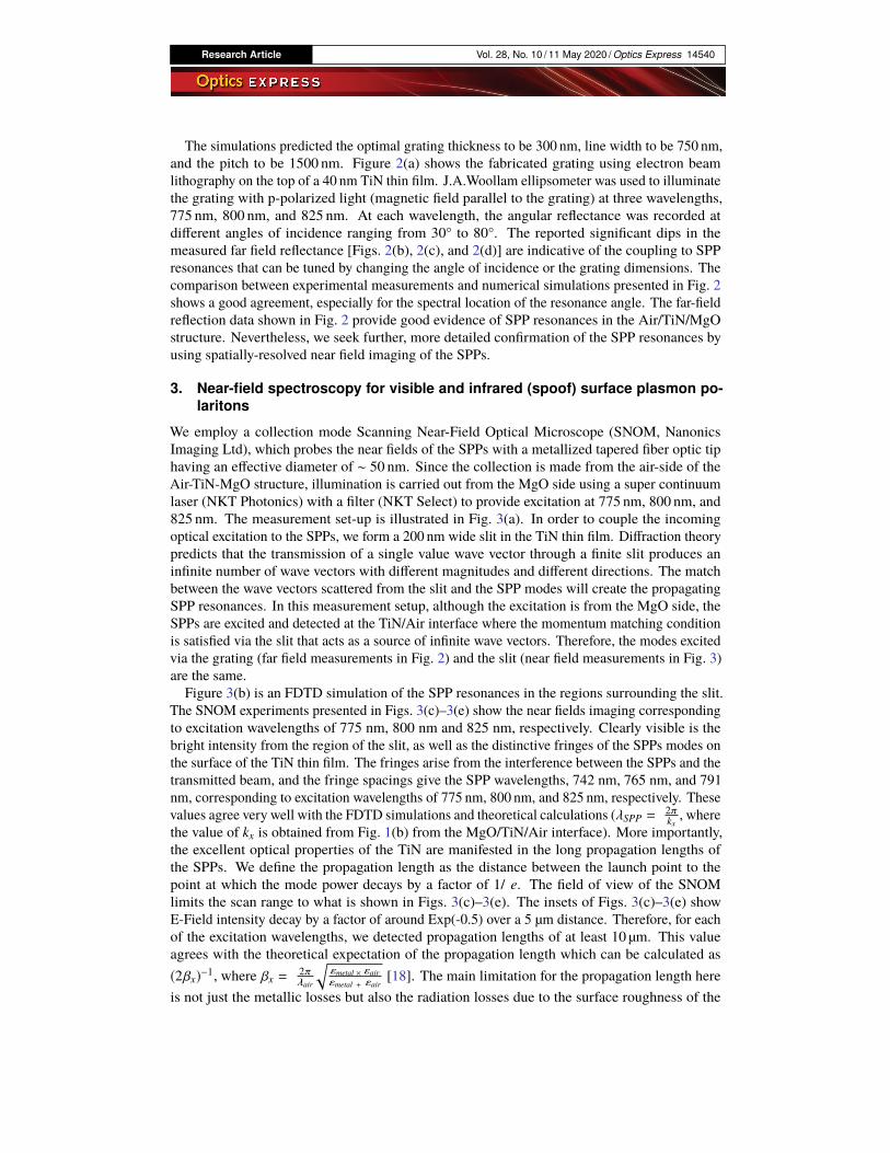
We employ a collection mode Scanning Near-Field Optical Microscope (SNOM, NanonicsImaging Ltd), which probes the near fields of the SPPs with a metallized tapered fiber optic tiphaving an effective diameter of ∼ 50 nm. Since the collection is made from the air-side of theAir-TiN-MgO structure, illumination is carried out from the MgO side using a super continuumlaser (NKT Photonics) with a filter (NKT Select) to provide excitation at 775 nm, 800 nm, and825 nm. The measurement set-up is illustrated in Fig. 3(a). In order to couple the incomingoptical excitation to the SPPs, we form a 200 nm wide slit in the TiN thin film. Diffraction theorypredicts that the transmission of a single value wave vector through a finite slit produces aninfinite number of wave vectors with different magnitudes and different directions. The matchbetween the wave vectors scattered from the slit and the SPP modes will create the propagatingSPP resonances. In this measurement setup, although the excitation is from the MgO side, theSPPs are excited and detected at the TiN/Air interface where the momentum matching conditionis satisfied via the slit that acts as a source of infinite wave vectors. Therefore, the modes excitedvia the grating (far field measurements in Fig. 2) and the slit (near field measurements in Fig. 3)are the same.Figure 3(b) is an FDTD simulation of the SPP resonances in the regions surrounding the slit.
The SNOM experiments presented in Figs. 3(c)–3(e) show the near fields imaging correspondingto excitation wavelengths of 775 nm, 800 nm and 825 nm, respectively. Clearly visible is thebright intensity from the region of the slit, as well as the distinctive fringes of the SPPs modes onthe surface of the TiN thin film. The fringes arise from the interference between the SPPs and thetransmitted beam, and the fringe spacings give the SPP wavelengths, 742 nm, 765 nm, and 791nm, corresponding to excitation wavelengths of 775 nm, 800 nm, and 825 nm, respectively. Thesevalues agree very well with the FDTD simulations and theoretical calculations (λSPP = 2π
kx , wherethe value of kx is obtained from Fig. 1(b) from the MgO/TiN/Air interface). More importantly,the excellent optical properties of the TiN are manifested in the long propagation lengths ofthe SPPs. We define the propagation length as the distance between the launch point to thepoint at which the mode power decays by a factor of 1/ e. The field of view of the SNOMlimits the scan range to what is shown in Figs. 3(c)–3(e). The insets of Figs. 3(c)–3(e) showE-Field intensity decay by a factor of around Exp(-0.5) over a 5 µm distance. Therefore, for eachof the excitation wavelengths, we detected propagation lengths of at least 10 µm. This valueagrees with the theoretical expectation of the propagation length which can be calculated as(2βx)−1, where βx = 2π
λair
√εmetal × εairεmetal + εair
[18]. The main limitation for the propagation length hereis not just the metallic losses but also the radiation losses due to the surface roughness of the
Research Article Vol. 28, No. 10 / 11 May 2020 / Optics Express 14541
6
Diffraction theory predicts that the transmission of a single value wave vector through a finite slit produces an infinite number of wave vectors with different magnitudes and different directions. The match between the wave vectors scattered from the slit and the SPP modes will create the propagating SPP resonances. In this measurement setup, although the excitation is
from the MgO side, the SPPs are excited and detected at the TiN/Air interface where the momentum matching condition is satisfied via the slit that acts as a source of infinite wave vectors. Therefore, the modes excited via the grating (far field measurements in Figure 2) and the slit (near field measurements in Figure 3) are the same.
Fig. 3. (a) SNOM measurement procedure (b) FDTD simulations for SPPs on TiN using slit coupling at 825 nm excitation. (c,d,e) SNOM results showing actual images of the SPPs with long propagation length of at least 10 μm for three excitation wavelengths: 775 nm, 800 nm, and 825 nm. Fast Fourier Transform of the data presented shows a dominant peak that corresponds to the periodicity of the fringes. The insets of figure c, d, and e labeled E-Field Intensity I(x) show the exponential power decay as a function of propagation distance x.
Figure 3b is an FDTD simulation of the SPP resonances in the regions surrounding the slit. The SNOM experiments presented in Figures 3c – 3e show the near fields imaging corresponding to excitation wavelengths of 775 nm, 800 nm and 825 nm, respectively. Clearly visible is the bright intensity from the region of the slit, as well as the distinctive fringes of the SPPs modes on the surface of the TiN thin film. The fringes arise from the interference between the SPPs
Fig. 3. (a) SNOM measurement procedure (b) FDTD simulations for SPPs on TiN usingslit coupling at 825 nm excitation. (c,d,e) SNOM results showing actual images of the SPPswith long propagation length of at least 10 µm for three excitation wavelengths: 775 nm, 800nm, and 825 nm. Fast Fourier Transform of the data presented shows a dominant peak thatcorresponds to the periodicity of the fringes. The insets of figure c, d, and e labeled E-FieldIntensity I(x) show the exponential power decay as a function of propagation distance x.
metallic thin film. This radiation loss can be overcome, thus increasing the propagation lengthto even centimeter range [24], by sandwiching the metallic thin film between two dielectricswith carefully designed dimensions creating a plasmonic waveguide as has been done previously[19–21,25,26]. Figure 3 gives evidence of a propagation length of 10 µm at 775 nm which isrelatively longer than previously-reported propagation lengths in bare metallic TiN thin films[3,5]
Figure 1(b) and the images shown in Figs. 2 and 3 demonstrate that TiN thin films can supportrobust SPPs with λSPP ∼ 750–800 nm. However, at the longer wavelengths, such as in the mid-IR,pertaining to the “phase-matched” region shown in Fig. 1(c) (< 250 THz or ∼ 1.2 µmwavelength),SPPs are not supported. The metallic TiN behaves as a perfect electric conductor, with an electricfield value dropping to zero at the interface, and the surface modes couple to radiative modes in

Research Article Vol. 28, No. 10 / 11 May 2020 / Optics Express 14542
the phase-matched region, also resulting in the loss of SPP confinement. However, Pendry et al.[27] realized that patterning the surface of the plasmonic material with etched holes or grooveswhose lateral dimensions are smaller than the wavelengths of interest creates an effective mediumthat satisfies the conditions needed for confined surface wave excitations [28]. The patternedsurface mimics or “spoofs” the behavior of metals in the visible regime, and these excitationsare termed Spoof Surface Plasmon Polaritons (SSPPs). Previous experimental detection ofSSPPs [29–31] have demonstrated that a significant depth of the trenches is necessary so thatthe grooves act as a cavity for the surface modes thus reducing their group velocity and stronglyincreasing their confinement at the interface. We explore the excitation of these SSPPs at 6µm using a 1D array of air-filled grooves etched into our TiN of width a, period d, and etcheddepth h. As explained in [32,33], the dispersion relation of SSPP TM modes in such effectivehomogenous anisotropic media is given by Eq. (3). Additionally, the complex wave vector (kg) ofthe evanescent fields inside the waveguide is given by Eq. (4).
kx2 = k02 +(akgtan (hkg)
d
)2(3)
kg2 = k02(1 +
i + 1ak0Re
√−εTiN
)(4)
k0 is the wave vector of the incident free modes in air, kg is the complex wave vectors ofthe evanescent modes propagating inside the guide, and kx is the wave vector of the SSPPsconfined modes propagating at the surface of the TiN grooves. Equations (3) and (4) providegreater accuracy than other analytical analyses that treat the metal as a perfect electric conductor[27,34], because they allow to explicitly incorporate the optical properties of TiN (εTiN) which
4
Fig. 4. (a, b, c, d) dispersion relation of SSPP at 50 nm, 200 nm, 500 nm, and 700 nm etch depth respectively. (e,f,g,h) Corresponding FDTD simulations showing the coupling from a 6 μm Total Field / Scattered Field excitation source (TF/SF) to SSPP on the surface of 50 nm, 200 nm, 500 nm, and 700 nm etch depth respectively. The red blob propagating upwards in plots f, g, and h represents reflections from the normally incident source. Figure h clearly shows the confined high intensity SSPP modes and the exponential evanescent behavior experienced inside the waveguides. The inset of Figure h shows a zoom in on the evanescent modes inside the trenches with saturated scale bar to highlight their decay behavior inside the guide. Visualization 1, Visualization 2, and Visualization 3 show the temporal evolution of the spoof plasmons for different etch depths in addition to the coupling and decoupling of radiative and confined states as the modes transition between flat and etched surfaces.
Fig. 4. (a, b, c, d) dispersion relation of SSPP at 50 nm, 200 nm, 500 nm, and 700 nm etchdepth respectively. (e,f,g,h) Corresponding FDTD simulations showing the coupling from a6 µm Total Field / Scattered Field excitation source (TF/SF) to SSPP on the surface of 50 nm,200 nm, 500 nm, and 700 nm etch depth respectively. The red blob propagating upwards inplots f, g, and h represents reflections from the normally incident source. Figure h clearlyshows the confined high intensity SSPP modes and the exponential evanescent behaviorexperienced inside the waveguides. The inset of Figure h shows a zoom in on the evanescentmodes inside the trenches with saturated scale bar to highlight their decay behavior insidethe guide. Visualization 1, Visualization 2, and Visualization 3 show the temporal evolutionof the spoof plasmons for different etch depths in addition to the coupling and decoupling ofradiative and confined states as the modes transition between flat and etched surfaces.
Research Article Vol. 28, No. 10 / 11 May 2020 / Optics Express 14543
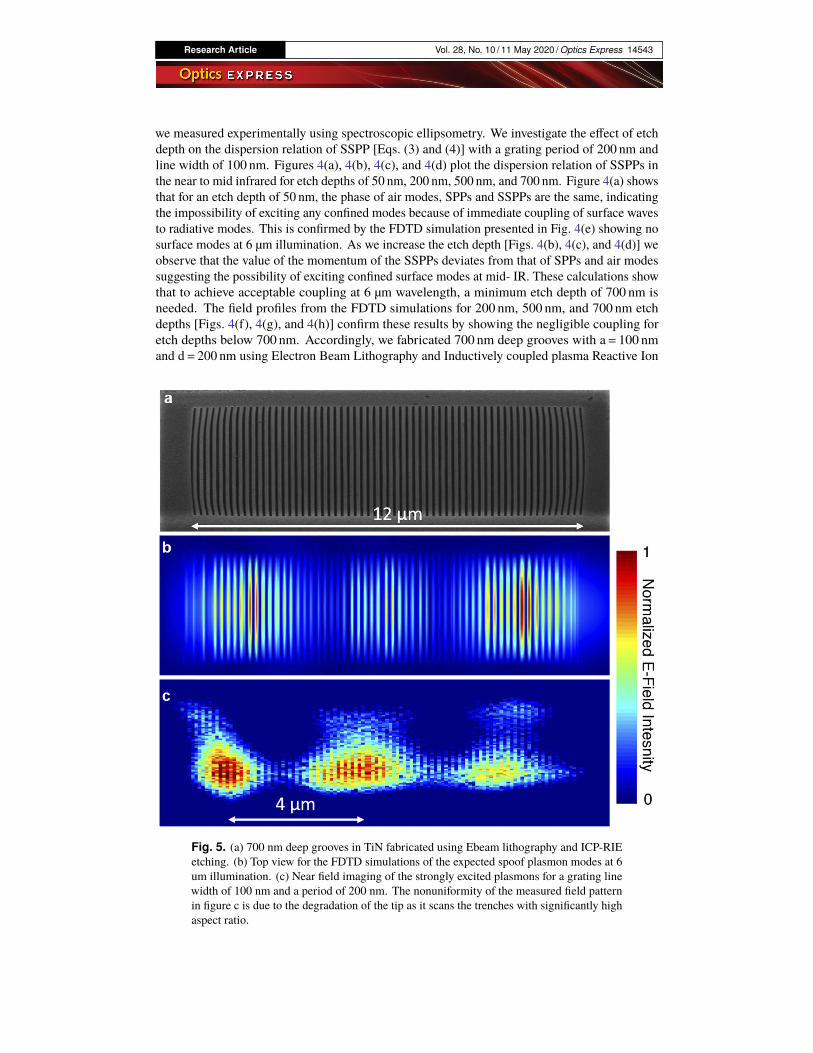
we measured experimentally using spectroscopic ellipsometry. We investigate the effect of etchdepth on the dispersion relation of SSPP [Eqs. (3) and (4)] with a grating period of 200 nm andline width of 100 nm. Figures 4(a), 4(b), 4(c), and 4(d) plot the dispersion relation of SSPPs inthe near to mid infrared for etch depths of 50 nm, 200 nm, 500 nm, and 700 nm. Figure 4(a) showsthat for an etch depth of 50 nm, the phase of air modes, SPPs and SSPPs are the same, indicatingthe impossibility of exciting any confined modes because of immediate coupling of surface wavesto radiative modes. This is confirmed by the FDTD simulation presented in Fig. 4(e) showing nosurface modes at 6 µm illumination. As we increase the etch depth [Figs. 4(b), 4(c), and 4(d)] weobserve that the value of the momentum of the SSPPs deviates from that of SPPs and air modessuggesting the possibility of exciting confined surface modes at mid- IR. These calculations showthat to achieve acceptable coupling at 6 µm wavelength, a minimum etch depth of 700 nm isneeded. The field profiles from the FDTD simulations for 200 nm, 500 nm, and 700 nm etchdepths [Figs. 4(f), 4(g), and 4(h)] confirm these results by showing the negligible coupling foretch depths below 700 nm. Accordingly, we fabricated 700 nm deep grooves with a= 100 nmand d= 200 nm using Electron Beam Lithography and Inductively coupled plasma Reactive Ion
Fig. 5. (a) 700 nm deep grooves in TiN fabricated using Ebeam lithography and ICP-RIEetching. (b) Top view for the FDTD simulations of the expected spoof plasmon modes at 6um illumination. (c) Near field imaging of the strongly excited plasmons for a grating linewidth of 100 nm and a period of 200 nm. The nonuniformity of the measured field patternin figure c is due to the degradation of the tip as it scans the trenches with significantly highaspect ratio.

Research Article Vol. 28, No. 10 / 11 May 2020 / Optics Express 14544
Etching (ICP-RIE) on a 1 µm thick TiN thin film. To experimentally validate the simulations,we obtained spatially-resolved near field images of the SSPPs in the patterned TiN film. Weobtained such images by carrying out apertureless scattering-type Scanning Near-field OpticalMicroscopy (s-SNOM) of 12 µm long etched trenches as shown in Fig. 5(a). The results ofthese measurements presented in Fig. 5(c) show strong SSPPs coupling with fringe spacing of4 µm. Figures 5(b) and 5(c) show a close match between our FDTD predictions and the nearfield measurements, confirming the excitation of confined surface plasmon modes in TiN at 6 µmillumination. The fringes observed in the simulations of the electric field profile of the spoofplasmons [Fig. 5(b)] are due to the excitation of standing SSPP waves. As the SSPPs make thetransition from the trench surface to the unpatterned surface, they experience reflections due tothe change in effective index between the two regions, resulting in a standing wave behavior.As done in our previous study of localized surface plasmon in TiN nano-antennas on silicon
[1], our s-SNOM analysis utilized a silicon tip coupled to an Atomic Force Microscopy (AFM)system, allowing for high spatial resolution 3D movement of the tip around the structure. Thegrating is illuminated by a 6 µm wavelength light source (a narrow-band quantum cascade laser,QCL) through a Michelson interferometer at an incidence angle of 60°. The silicon tip, in tappingmode on the sample, becomes polarized by the laser source and itself acts as a local antennathat scatters the near field from the surface of the grating, modulating the light with the tappingfrequency. A moving mirror, oscillating at the same frequency as the tip is used to implementpseudo-heterodyne demodulation of the phase and amplitude of the scattered field. Images ofamplitude, such as that shown in Fig. 5(c), are formed by raster scans of the tip over the grating’ssurface in the (x, y) plane. This setup allows for the detection of the magnitude and phase ofthe out-of-plane electric field component (Ez) only. It is worth mentioning that because of thehigh aspect ratio of the grating, the tip gets damaged during the scanning and often breaks downbefore the end of the scan. Several measurements had to be taken to be able to scan a 12 µm longgrating, during which the tip quality was degraded, resulting in the non-uniform E-field patternin Fig. 5(c).
4. Conclusion
We have demonstrated the plasmonic capabilities of TiN thin films deposited under conditionsthat produced high metallic quality and low loss. Such films produced strong SPP resonances,which we were able to directly image in the near field for both visible and infrared wavelengths.Near-field imaging indicates propagation lengths longer than 10 µm, We note that althoughprevious reports [3,5,35] have presented mathematical calculations for SPP propagation lengths inTiN thin films, no experimental imaging of the plasmons nor measurements of their propagationlengths have been hitherto reported. Additionally, we explored the excitation of Spoof SPPs onthe surface of our TiN thin films in the mid-IR region, and provided near-field images usingscattering s-SNOM.
Funding
National Science Foundation (1839164-PHY: RAISE-TAQS, ECCS-1541959, ECCS-1748106:EAGER).
Acknowledgments
The authors gratefully acknowledge Andy Greenspon, Michele Tamagnone and Stephan Kraemerdiscussions on fabrication and measurements.

Research Article Vol. 28, No. 10 / 11 May 2020 / Optics Express 14545
Disclosures
The authors declare no conflicts of interest.
References1. M. N. Gadalla, A. S. Greenspon, M. Tamagnone, F. Capasso, and E. L. Hu, “Excitation of Strong Localized
Surface Plasmon Resonances in Highly Metallic Titanium Nitride Nano-Antennas for Stable Performance at ElevatedTemperatures,” ACS Appl. Nano Mater. 2(6), 3444–3452 (2019)..
2. U. Guler, A. Boltasseva, and V. M. Shalaev, “Refractory plasmonics,” Science 344(6181), 263–264 (2014).3. G. V. Naik, J. L. Schroeder, X. Ni, A. V. Kildishev, T. D. Sands, and A. Boltasseva, “Titanium nitride as a plasmonic
material for visible and near-infrared wavelengths,” Opt. Mater. Express 2(4), 478–489 (2012).4. U. Guler, D. Zemlyanov, J. Kim, Z. Wang, R. Chandrasekar, X. Meng, E. Stach, A. V. Kildishev, V. M. Shalaev, and
A. Boltasseva, “Plasmonic Titanium Nitride Nanostructures via Nitridation of Nanopatterned Titanium Dioxide,”Adv. Opt. Mater. 5(7), 1600717 (2017).
5. H. Reddy, U. Guler, Z. Kudyshev, A. V. Kildishev, V. M. Shalaev, and A. Boltasseva, “Temperature-DependentOptical Properties of Plasmonic Titanium Nitride Thin Films,” ACS Photonics 4(6), 1413–1420 (2017)..
6. G. V. Naik, B. Saha, J. Liu, S. M. Saber, E. A. Stach, J. M. Irudayaraj, T. D. Sands, V. M. Shalaev, and A. Boltasseva,“Epitaxial superlattices with titanium nitride as a plasmonic component for optical hyperbolic metamaterials,” Proc.Natl. Acad. Sci. 111(21), 7546–7551 (2014)..
7. C. M. Zgrabik and E. L. Hu, “Optimization of sputtered titanium nitride as a tunable metal for plasmonic applications,”Opt. Mater. Express 5(12), 2786–2797 (2015)..
8. W.-P. Guo, R. Mishra, C.-W. Cheng, B.-H. Wu, L.-J. Chen, M.-T. Lin, and S. Gwo, “Titanium Nitride Epitaxial Filmsas a Plasmonic Material Platform: Alternative to Gold,” ACS Photonics 6(8), 1848–1854 (2019)..
9. R. P. Sugavaneshwar, S. Ishii, T. D. Dao, A. Ohi, T. Nabatame, and T. Nagao, “Fabrication of highly metallic TiNfilms by pulsed laser deposition method for plasmonic applications,” ACS Photonics 5(3), 814–819 (2018).
10. N. Kinsey, M. Ferrera, G. V. Naik, V. Babicheva, V. M. Shalaev, and A. Boltasseva, “Experimental demonstration oftitanium nitride plasmonic interconnects,” Opt. Express 22(10), 12238–12247 (2014).
11. C. Vernoux, Y. Chen, L. Markey, C. Spârchez, J. Arocas, T. Felder, M. Neitz, L. Brusberg, J.-C. Weeber, and S. I.Bozhevolnyi, “Flexible long-range surface plasmon polariton single-mode waveguide for optical interconnects,” Opt.Mater. Express 8(2), 469–484 (2018).
12. C. M. Zgrabik, Wide tunability of magnetron sputtered titanium nitride and titanium oxynitride for plasmonicapplications (2016).
13. M. Gadalla, A. Greenspon, M. Tamagnone, F. Capasso, and E. Hu, “Metallic refractory titanium nitride: Analternative stable metal with tunable optical properties for high temperature plasmonic applications,” in APS MeetingAbstracts (2019).
14. N. White, A. Campbell, J. Grant, R. Pachter, K. Eyink, R. Jakubiak, G. Martinez, and C. Ramana, “Surface/interfaceanalysis and optical properties of RF sputter-deposited nanocrystalline titanium nitride thin films,” Appl. Surf. Sci.292, 74–85 (2014).
15. J. Rivory, J. Behaghel, S. Berthier, and J. Lafait, “Structure and properties of TiN coatings,” Thin Solid Films 78(2),161–165 (1981).
16. P. Patsalas and S. Logothetidis, “Optical, electronic, and transport properties of nanocrystalline titanium nitride thinfilms,” J. Appl. Phys. 90(9), 4725–4734 (2001)..
17. W. M. Haynes, Crc handbook of chemistry and physics (CRC press, 2014).18. S. A. Maier, Plasmonics: Fundamentals and applications (Springer Science & Business Media, 2007).19. J. Chen, Z. Li, S. Yue, and Q. Gong, “Hybrid long-range surface plasmon-polariton modes with tight field confinement
guided by asymmetrical waveguides,” Opt. Express 17(26), 23603–23609 (2009).20. M.-S. Tomaš and Z. Lenac, “Long-range surface polaritons in a supported thin metallic slab,” Solid State Commun.
50(10), 915–918 (1984).21. M.-S. Tomaš and Z. Lenac, “Coupled surface polariton with guided wave polariton modes in asymmetric metal clad
dielectric waveguides,” Opt. Commun. 55(4), 267–270 (1985).22. Z. Lenac, “Attenuation of long-range surface polaritons in a thin metallic slab with a dielectric coating,” Surf. Sci.
154(2-3), 639–657 (1985).23. http://www.nanophys.kth.se/nanophys/facilities/nfl/resists/zep520a-7-2.pdf.24. P. Berini, “Long-range surface plasmon polaritons,” Adv. Opt. Photonics 1(3), 484–588 (2009).25. W.Ma and A. S. Helmy, “Asymmetric long-range hybrid-plasmonic modes in asymmetric nanometer-scale structures,”
J. Opt. Soc. Am. B 31(7), 1723–1729 (2014)..26. S. Saha, A. Dutta, N. Kinsey, A. V. Kildishev, V. M. Shalaev, and A. Boltasseva, “On-Chip Hybrid Photonic-Plasmonic
Waveguides with Ultrathin Titanium Nitride Films,” ACS Photonics 5(11), 4423–4431 (2018)..27. J. Pendry, L. Martin-Moreno, and F. Garcia-Vidal, “Mimicking Surface Plasmons with Structured Surfaces,” Science
305(5685), 847–848 (2004).28. M. Born and E. Wolf, Principles of optics: Electromagnetic theory of propagation, interference and diffraction of
light (Elsevier, 2013).

Research Article Vol. 28, No. 10 / 11 May 2020 / Optics Express 14546
29. N. Yu, Q. J. Wang, M. A. Kats, J. A. Fan, S. P. Khanna, L. Li, A. G. Davies, E. H. Linfield, and F. Capasso, “Designerspoof surface plasmon structures collimate terahertz laser beams,” Nat. Mater. 9(9), 730–735 (2010).
30. J. Y. Yin, J. Ren, H. C. Zhang, B. C. Pan, and T. J. Cui, “Broadband Frequency-Selective Spoof Surface PlasmonPolaritons on Ultrathin Metallic Structure,” Sci. Rep. 5(1), 8165 (2015)..
31. Z. Liao, Y. Luo, A. I. Fernández-Domínguez, X. Shen, S. A. Maier, and T. J. Cui, “High-order localized spoof surfaceplasmon resonances and experimental verifications,” Sci. Rep. 5(1), 9590 (2015)..
32. A. Rusina, M. Durach, and M. I. Stockman, “Theory of spoof plasmons in real metals,” Appl. Phys. A 100(2),375–378 (2010).
33. A. Rusina, M. Durach, K. A. Nelson, and M. I. Stockman, “Nanoconcentration of terahertz radiation in plasmonicwaveguides,” Opt. Express 16(23), 18576–18589 (2008).
34. F. Garcia-Vidal, L. Martin-Moreno, and J. Pendry, “Surfaces with holes in them: new plasmonic metamaterials,” J.Opt. A: Pure Appl. Opt. 7(2), S97–S101 (2005).
35. M. Cortie, J. Giddings, and A. Dowd, “Optical properties and plasmon resonances of titanium nitride nanostructures,”Nanotechnology 21(11), 115201 (2010).