Embed Size (px)
Citation preview
HAL Id: hal-01100102https://hal.archives-ouvertes.fr/hal-01100102
Submitted on 12 Jan 2015
HAL is a multi-disciplinary open accessarchive for the deposit and dissemination of sci-entific research documents, whether they are pub-lished or not. The documents may come fromteaching and research institutions in France orabroad, or from public or private research centers.
L’archive ouverte pluridisciplinaire HAL, estdestinée au dépôt et à la diffusion de documentsscientifiques de niveau recherche, publiés ou non,émanant des établissements d’enseignement et derecherche français ou étrangers, des laboratoirespublics ou privés.
Impact of Blend Morphology on Interface StateRecombination in Bulk Heterojunction Organic Solar
CellsBenjamin Bouthinon, Raphaël Clerc, Jérôme Vaillant, J.-M Verilhac, Jérôme
Faure-Vincent, David Djurado, Irina Ionica, Gabriel Man, Antoine Gras,Georges Pananakakis, et al.
To cite this version:Benjamin Bouthinon, Raphaël Clerc, Jérôme Vaillant, J.-M Verilhac, Jérôme Faure-Vincent, etal.. Impact of Blend Morphology on Interface State Recombination in Bulk HeterojunctionOrganic Solar Cells. Advanced Functional Materials, Wiley, 2015, pp.10.1002/adfm.201401633.<10.1002/adfm.201401633>. <hal-01100102>
1
DOI: 10.1002/ ((please add manuscript number))
Article type: Full Paper
Title: Impact of blend morphology on interface state recombinations in bulk heterojunction
organic solar cells
Author(s), and Corresponding Author(s)*: Benjamin Bouthinon , Raphaël Clerc , Jérôme
Vaillant , Jean-Marie Verilhac , Jérôme Faure-Vincent , David Djurado , Irina Ionica ,
Gabriel Man , Antoine Gras , Georges Pananakakis , Romain Gwoziecki , and Antoine Kahn
B. Bouthinon*, Dr. J. Vaillant, Dr. J.-M. Verilhac, A. Gras, Dr. R. Gwoziecki
CEA, LITEN, Laboratoire des Composants Electroniques Imprimés, F-38054 Grenoble,
France.
E-mail: [email protected]
Prof. R. Clerc
Laboratoire Hubert Curien, UMR CNRS 5516, Université Jean Monnet, Institut d’Optique
Graduate School, F-42000 Saint-Etienne, France.
Dr. J. Faure-Vincent, Dr. D. Djurado
CEA, INAC, Structure des Propriétés d’Architectures Moléculaires UMR5819, F-38054
Grenoble, France.
Dr. I. Ionica, Prof. G. Pananakakis
IMEP LAHC, Grenoble INP – Minatec, F-38016 Grenoble, France.
G. Man, Prof. A. Kahn
Department of Electrical Engineering, Princeton University, Princeton NJ, 08544,USA
Keywords: bulk heterojunction, interface state, morphology, annealing, solar cell
This work is a re-investigation of the impact of blend morphology and thermal annealing on
the electrical performance of regioregular P3HT:PC60BM. The blend is first characterized by
combining atomic force microscopy, X-rays diffraction and Time-of-Flight experiments. Then,
current-voltage characteristics of photodiode devices are measured in the dark and under
illumination. Finally, the existence of exponential tails of electronic gap states is
experimentally confirmed by measuring the device spectral response in the sub-band gap
regime. This method reveals the existence of a large density of gap states, which is partially
reduced by successive annealing steps. The comparison between drift and diffusion
simulations and charge transport experiments show that, when band gap tails are properly
2
taken into account, simulations can satisfactorily reproduce experimental currents under both
dark and illumination conditions as a function of voltage and annealing time. This work
further confirms the critical impact of tails states on the performance of solar cells.
1. Introduction
Large area, low weight, cost effectiveness and flexibility are some of the exciting
promises of printed organic solar cells.[1–4]
Since the introduction of the organic diode concept
by Tang et al in 1986[5]
, the performances of such devices, produced by printing technologies,
have considerably been improved, reaching the record power conversion efficiency of
11.1%.[6]
Bulk HeteroJunction solar cell (BHJ) are one of the most common type of printed
organic photovoltaic device.[7]
This structure offers not only an excellent tradeoff between
optimal charge transfer[8]
and exciton dissociation at the donor/acceptor interface[9]
, but also a
good collection of photo-generated carriers.
As pointed out in many papers [10–13]
, the intimate organization of the interpenetrating
network composed of the acceptor-like material (fullerene) and the donor-like material
(polymer) is of critical importance, directly impacting the cell electro-optical performance.
Indeed photon absorption, exciton dissociation and carrier collection are morphology
dependent parameters.[9,14–17]
For this reason, the optimization of BHJ blend morphology has been considerably
investigated, essentially by means of atomic force microscopy (AFM) phase measurement in
tapping mode[18]
or by transmission electron microscopy (TEM)[19,20]
, whereas changes in
crystallization were usually probed by X-rays diffraction measurements.[21]
In these previous investigations, several parameters impacting the morphology were identified,
such as the nature of the solvent[22]
, the use of solvent additives[23,24]
, the deposition
method[25,26]
, the polymer/fullerene ratio[27,28]
, the polymer and fullerene crystallization state
3
[12,29–32], the nature of the fullerene material
[33] and one of the most studied, the blend
annealing (duration, temperature).[34,35]
The physical understanding of the relationship between efficiency and morphology
was recently improved. Several authors have simulated the performances of such cells,
explicitly taking into account morphology and using Kinetic Monte Carlo[11,17,36,37]
or 3-D
Drift Diffusion approaches.[38,39]
These studies concluded on the existence of an ideal
morphology resulting from the competition between exciton dissociation (penalized by too
large domains) and Langevin recombinations (enhanced by too narrow domains).
This picture is however still incomplete, as it ignores another significant
recombination mechanisms, such as trap-assisted recombination. Indeed, Street and
coworkers[40,41]
have pointed out trap-assisted recombination, as one of the major sources of
efficiency losses in Poly(3-hexylthiophene-2,5-diyl) (P3HT):[6,6]-Phenyl-C61-butyric acid
methyl ester (PC60BM) and Poly[N-9'-heptadecanyl-2,7-carbazole-alt-5,5-(4',7'-di-2-thienyl-
2',1',3'-benzothiadiazole)] (PCDTBT):[6,6]-Phenyl-C71-butyric acid methyl ester (PC70BM)
solar cells.[42,43]
This conclusion was reached using spectral response measurements in the
near IR region, probing sub-band gap transitions from trap level states to the HOMO or
LUMO bands. However, as measurements were performed in devices featuring a given
morphology, little was extracted about the correlation between morphology and trap
distribution and density.
In particular, it is well known that either Langevin or trap assisted recombinations
mostly occur at the donor acceptor interface. For this reason, it is unclear whether annealing
impacts performance mostly by changing the morphology of the blend (i.e. the interface
volume fraction) or by modifying the recombination properties of the blend (transport
properties, trap concentration).
The aim of this paper is to investigate the impact of morphology on trap assisted
recombination in BHJ solar cells. In this contribution, the blend morphology is modified by
4
successive post-processing thermal treatments at 85°C. Both the blend morphology and the
solar cell properties are characterized between each annealing sequence. The spectral
response of the device in the near infrared (IR) region is recorded to probe how the band gap
states evolve during the experiment. In addition, a numerical model (based on a one-
dimensional drift-diffusion formalism), properly calibrated on experiments, is implemented,
accounting for the measured exponential trap density of states. The conclusion obtained from
comparing experiments and simulations are discussed in the last section of the paper.
2. Experimental Section
The devices had the following general structure: ITO/PEDOT:PSS/P3HT:PC60BM/Al.
Regioregular poly(3-hexylthiophene-2,5-diyl) (P3HT) and Phenyl-C61-butyric acid methyl
ester (PC60BM) were purchased from Merck. Poly(3,4-ethylenedioxythiophene)
(PEDOT:PSS) was purchased from Heraeus with the grade named, CLEVIOS P VP AI 4083.
ITO-coated glass substrates were cleaned by successive 10 min. sonication sequences in EDI
(water electrodeionization), acetone and isopropanol. A PEDOT:PSS layer used as hole-
injection layer was spin-coated at 2000 rpm for 50 seconds to form a 40 nm film on top of the
ITO substrate. Then samples were dried at 115°C under nitrogen for 20 minutes. A 50 mg/ml
solution of P3HT:PC60BM was solubilized in chlorobenzene with a prepared blend ratio of
1:1 (weight ratio). Diiodooctane (DIO) was added to the solution (5% in volume) in order to
dissolve selectively the fullerene molecules, preventing C60 aggregation[24,44,45]
. When the
chlorobenzene starts evaporating, the fullerene is kept soluble in a semi-crystalline matrix of
P3HT by the DIO additive, as its melting point is higher than that of chlorobenzene (169°C vs.
131°C). DIO has been used in all experiments, in particular to improve the degree of
crystallinity of P3HT domains (see later).
The P3HT:PC60BM blend layer was spin-coated at 800 rpm for 3 minutes in air. The typical
thickness of the active layer was 330nm (measured by mechanical profilometer). Note that
5
this large value of the active layer, prejudicial for solar cell performances, is needed in
this work, in order to keep the level of dark current low. Indeed, it would no longer be
possible to measure accurately the EQE at low photon energy if the dark current is too
large.
No post-annealing treatment was done after this initial step. Finally, 100 nm thick aluminum
cathode contacts were evaporated via shadow mask in a vacuum chamber under a pressure of
10-6
mbar. Samples were stored one day in a nitrogen-filled glove box and then encapsulated
with a glass cover. The device area was 3.14 mm².
For thermal annealing, the encapsulated photodiode was annealed in nitrogen on a hot
plate at 85°C. This low temperature was selected to prevent the C60 diffusion usually observed
at higher temperatures.[13]
3. Experimental results
3.1. Physical characterization of blend morphology
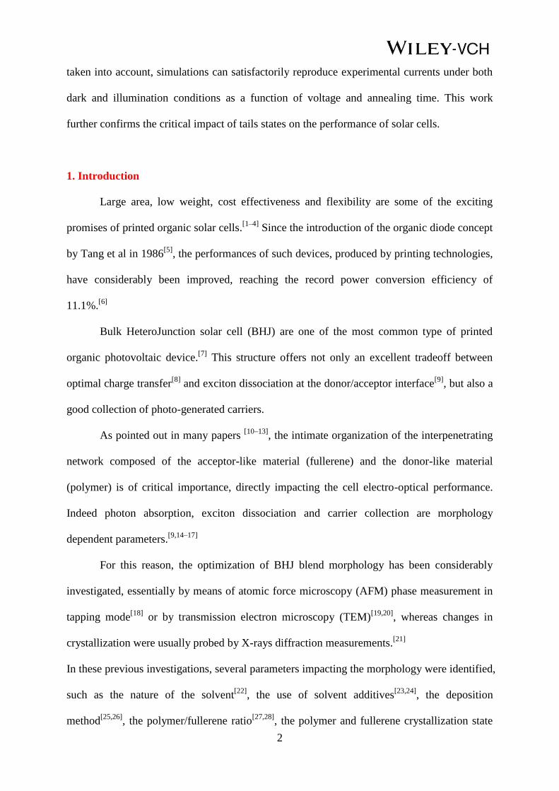
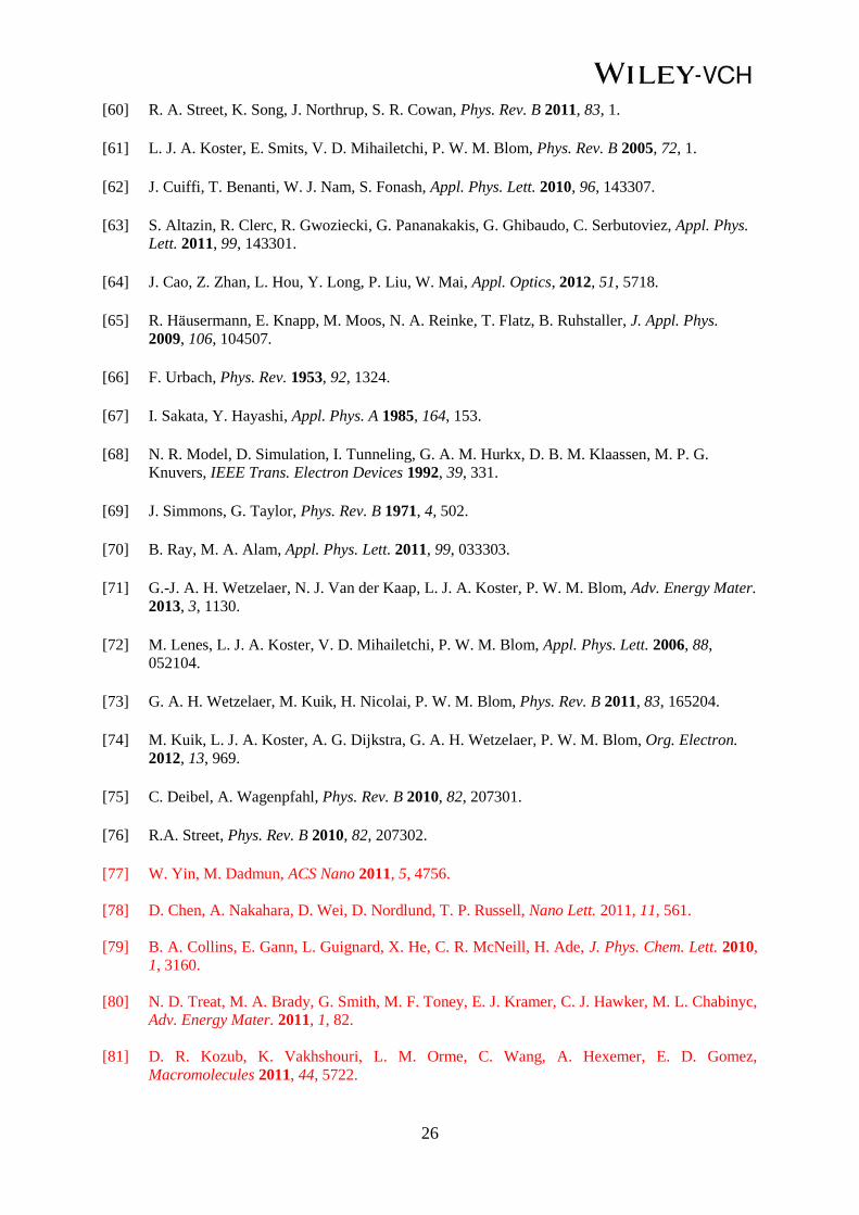
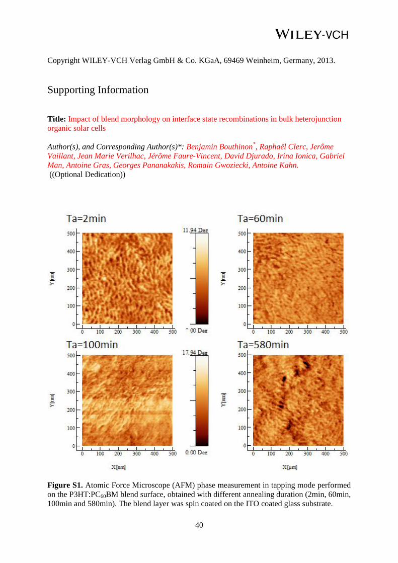
AFM tapping mode measurements were performed on the surface of P3HT:PC60BM
blends for different annealing steps in order to monitor the average domain width evolution
with annealing. Topography and phase were both recorded during tip scan and results are
reported in Figure S1. Phase measurement is known to reveal crystallized regions[18,46]
, taking
advantage here of the easily observable fibrous aspect of P3HT. The average width of the
P3HT domains is extracted from AFM phase images using an autocorrelation procedure,
performed numerically on the raw data. In accord with Dante et al.[18]
, we measure an average
domain width increase during annealing (Figure 1). Moreover, this domain growth is found to
follow the kinetics introduced by Alam et al[47]
given by :
n
eff0tDWtW (1)
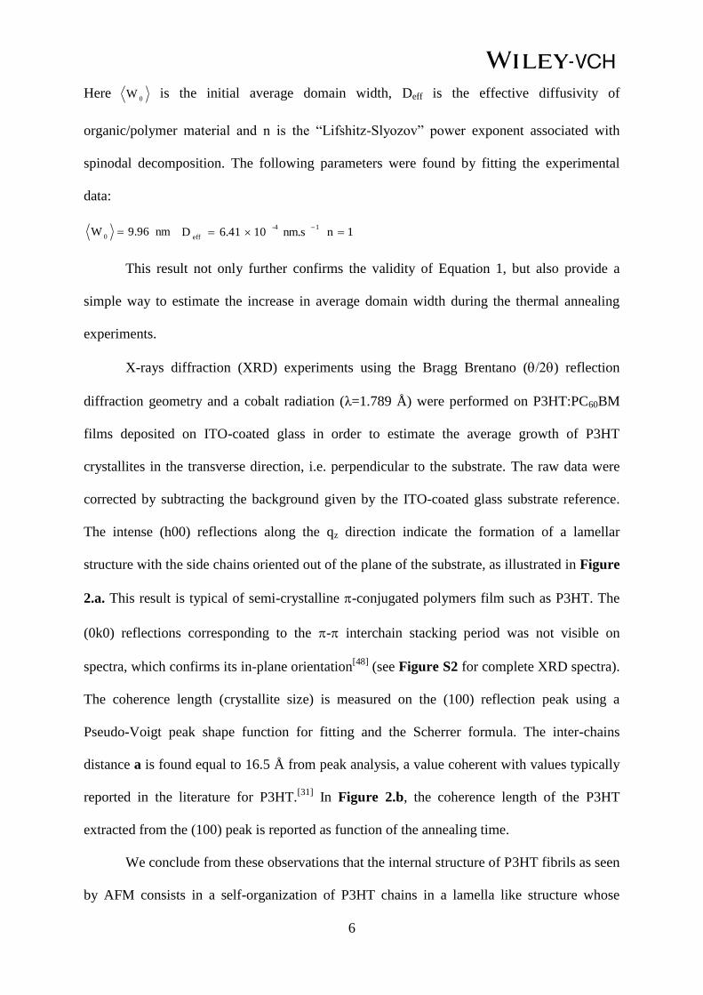
6
Here 0
W is the initial average domain width, Deff is the effective diffusivity of
organic/polymer material and n is the “Lifshitz-Slyozov” power exponent associated with
spinodal decomposition. The following parameters were found by fitting the experimental
data:
nm 9.96W0
1-4
effnm.s 10 6.41D
1n
This result not only further confirms the validity of Equation 1, but also provide a
simple way to estimate the increase in average domain width during the thermal annealing
experiments.
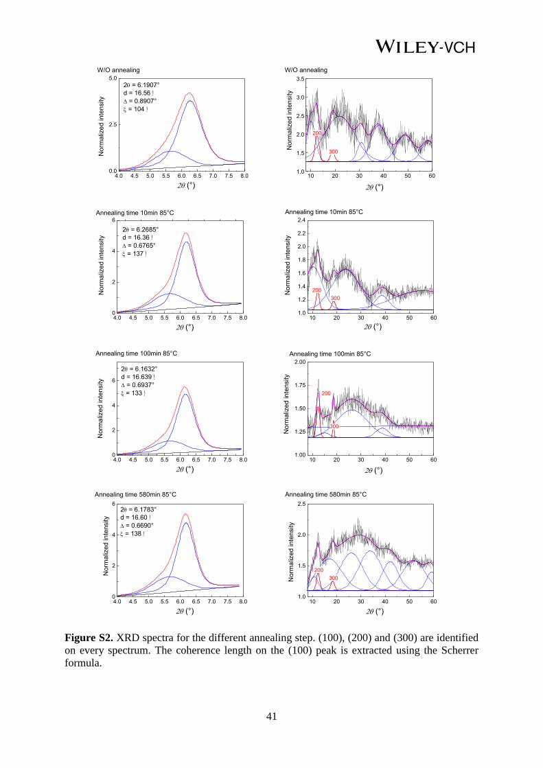
X-rays diffraction (XRD) experiments using the Bragg Brentano () reflection
diffraction geometry and a cobalt radiation (λ=1.789 Å) were performed on P3HT:PC60BM
films deposited on ITO-coated glass in order to estimate the average growth of P3HT
crystallites in the transverse direction, i.e. perpendicular to the substrate. The raw data were
corrected by subtracting the background given by the ITO-coated glass substrate reference.
The intense (h00) reflections along the qz direction indicate the formation of a lamellar
structure with the side chains oriented out of the plane of the substrate, as illustrated in Figure
2.a. This result is typical of semi-crystalline -conjugated polymers film such as P3HT. The
(0k0) reflections corresponding to the - interchain stacking period was not visible on
spectra, which confirms its in-plane orientation[48]
(see Figure S2 for complete XRD spectra).
The coherence length (crystallite size) is measured on the (100) reflection peak using a
Pseudo-Voigt peak shape function for fitting and the Scherrer formula. The inter-chains
distance a is found equal to 16.5 Å from peak analysis, a value coherent with values typically
reported in the literature for P3HT.[31]
In Figure 2.b, the coherence length of the P3HT
extracted from the (100) peak is reported as function of the annealing time.
We conclude from these observations that the internal structure of P3HT fibrils as seen
by AFM consists in a self-organization of P3HT chains in a lamella like structure whose
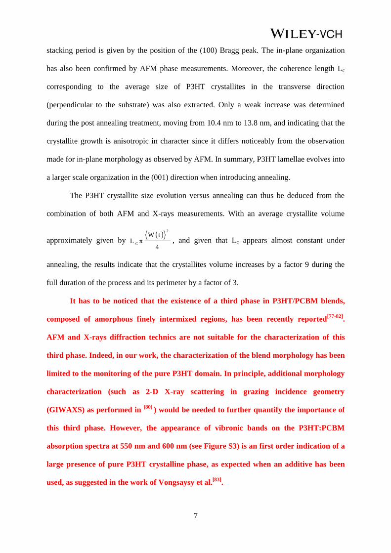
7
stacking period is given by the position of the (100) Bragg peak. The in-plane organization
has also been confirmed by AFM phase measurements. Moreover, the coherence length Lc
corresponding to the average size of P3HT crystallites in the transverse direction
(perpendicular to the substrate) was also extracted. Only a weak increase was determined
during the post annealing treatment, moving from 10.4 nm to 13.8 nm, and indicating that the
crystallite growth is anisotropic in character since it differs noticeably from the observation
made for in-plane morphology as observed by AFM. In summary, P3HT lamellae evolves into
a larger scale organization in the (001) direction when introducing annealing.
The P3HT crystallite size evolution versus annealing can thus be deduced from the
combination of both AFM and X-rays measurements. With an average crystallite volume
approximately given by
4
tWπL
2
C, and given that Lc appears almost constant under
annealing, the results indicate that the crystallites volume increases by a factor 9 during the
full duration of the process and its perimeter by a factor of 3.
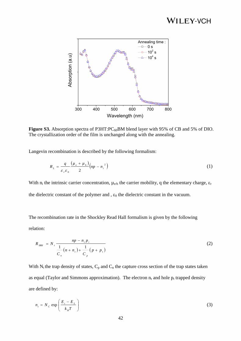
It has to be noticed that the existence of a third phase in P3HT/PCBM blends,
composed of amorphous finely intermixed regions, has been recently reported[77-82]
.
AFM and X-rays diffraction technics are not suitable for the characterization of this
third phase. Indeed, in our work, the characterization of the blend morphology has been
limited to the monitoring of the pure P3HT domain. In principle, additional morphology
characterization (such as 2-D X-ray scattering in grazing incidence geometry
(GIWAXS) as performed in [80]
) would be needed to further quantify the importance of
this third phase. However, the appearance of vibronic bands on the P3HT:PCBM
absorption spectra at 550 nm and 600 nm (see Figure S3) is an first order indication of a
large presence of pure P3HT crystalline phase, as expected when an additive has been
used, as suggested in the work of Vongsaysy et al.[83]
.
8
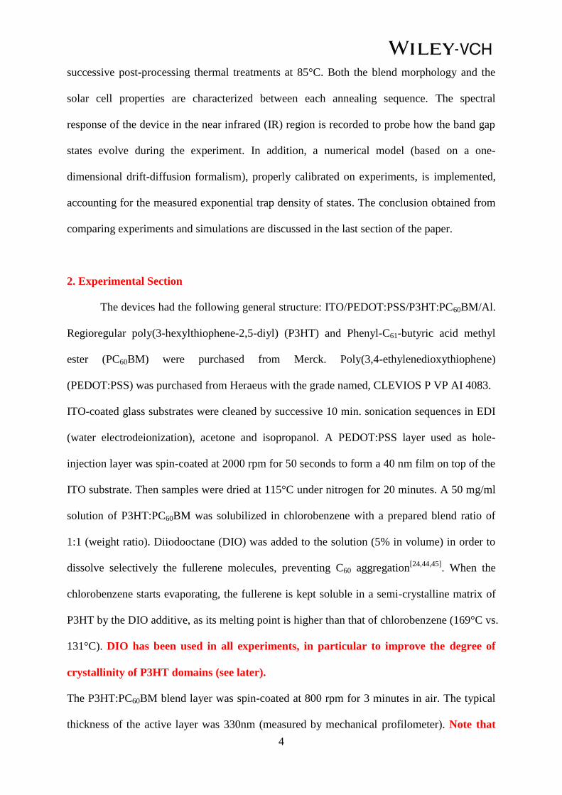
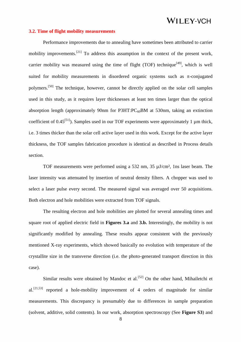
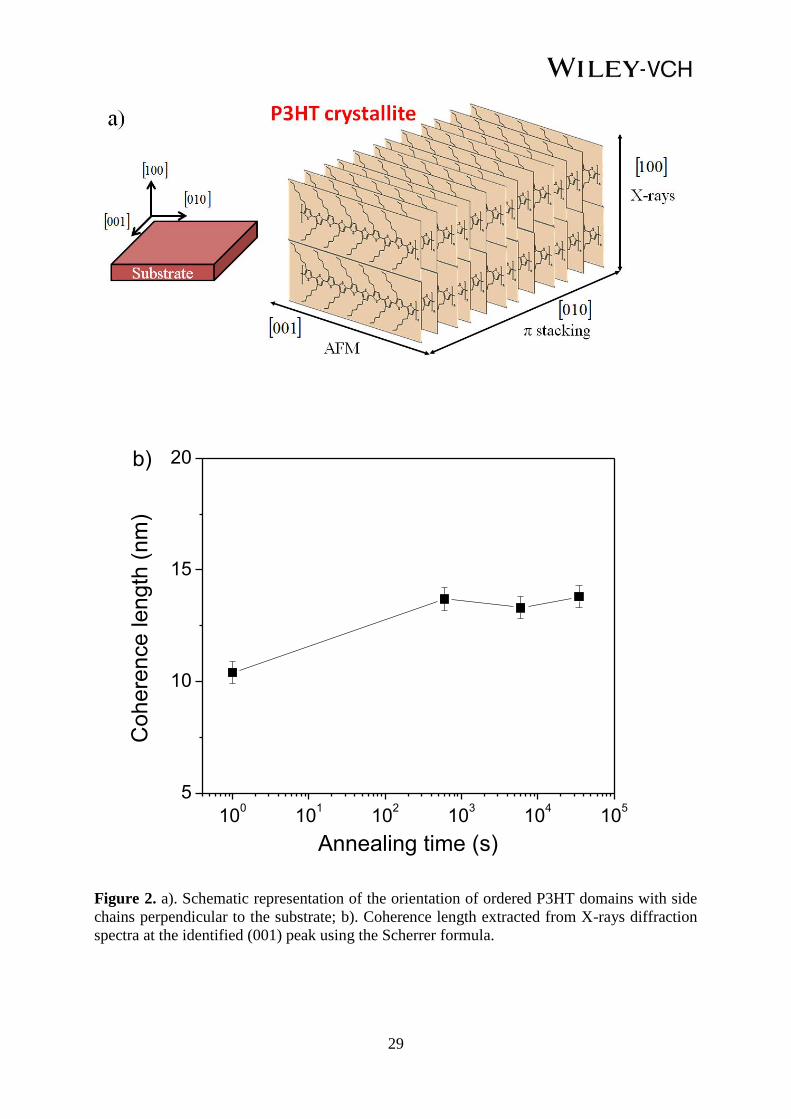
3.2. Time of flight mobility measurements
Performance improvements due to annealing have sometimes been attributed to carrier
mobility improvements.[21]
To address this assumption in the context of the present work,
carrier mobility was measured using the time of flight (TOF) technique[49]
, which is well
suited for mobility measurements in disordered organic systems such as -conjugated
polymers.[50]
The technique, however, cannot be directly applied on the solar cell samples
used in this study, as it requires layer thicknesses at least ten times larger than the optical
absorption length (approximately 90nm for P3HT:PC60BM at 530nm, taking an extinction
coefficient of 0.45[51]
). Samples used in our TOF experiments were approximately 1 µm thick,
i.e. 3 times thicker than the solar cell active layer used in this work. Except for the active layer
thickness, the TOF samples fabrication procedure is identical as described in Process details
section.
TOF measurements were performed using a 532 nm, 35 µJ/cm², 1ns laser beam. The
laser intensity was attenuated by insertion of neutral density filters. A chopper was used to
select a laser pulse every second. The measured signal was averaged over 50 acquisitions.
Both electron and hole mobilities were extracted from TOF signals.
The resulting electron and hole mobilities are plotted for several annealing times and
square root of applied electric field in Figures 3.a and 3.b. Interestingly, the mobility is not
significantly modified by annealing. These results appear consistent with the previously
mentioned X-ray experiments, which showed basically no evolution with temperature of the
crystallite size in the transverse direction (i.e. the photo-generated transport direction in this
case).
Similar results were obtained by Mandoc et al.[52]
On the other hand, Mihailetchi et
al.[21,53]
reported a hole-mobility improvement of 4 orders of magnitude for similar
measurements. This discrepancy is presumably due to differences in sample preparation
(solvent, additive, solid contents). In our work, absorption spectroscopy (See Figure S3) and
9
X-rays diffraction measurements reveal that the ratio of the volume of crystallized P3HT to
the total volume is approximately equal to 60% before annealing. Although this ratio was not
specified in the work of Mihailetchi et al., the extreme low value of their hole mobility before
annealing ( 10-8
cm2.V
-1.s
-1, compared to 10
-4 cm
2.V
-1.s
-1 in our work) suggests a much
lower concentration of crystallized P3HT fraction before annealing. Moreover, mobility in
that work was not measured by TOF, but extracted from an I-V curve fitting using a space
charge limited current (SCLC) model, which renders a quantitative comparison with mobility
values reported in our work questionable.
Finally, experiments show a decreasing mobility with electric field for both electrons
and holes, which is rather unexpected for most polymers, but typical of energetic and spatial
disorder in P3HT material.[54,55]
Experiments can be fitted by the model proposed in[56]
: this
empirical model is then used to calibrate numerical simulations.
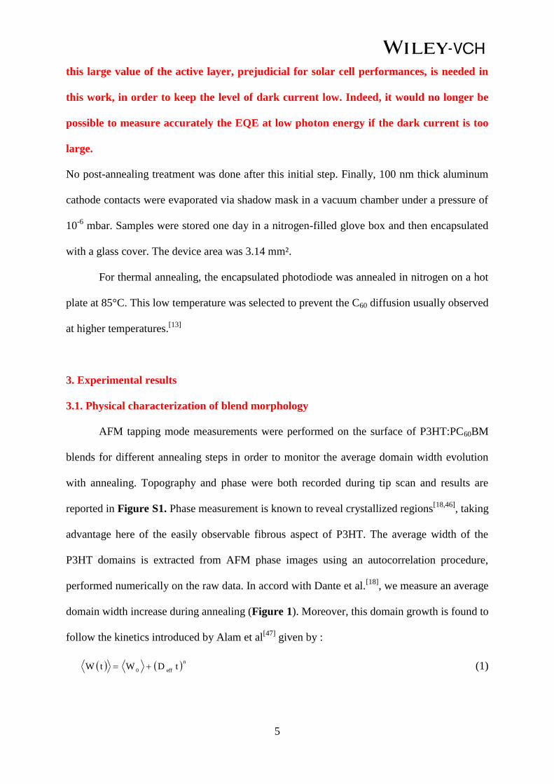
3.3. Impact of morphology on I-V and visible EQE measurements
Photocurrents, External Quantum Efficiency (EQE), as well as dark currents were
measured after each annealing step in order to monitor the impact of annealing on diode
performances.
First, photocurrent measurements in short circuit condition were performed at two different
wavelengths, 440 nm and 620 nm, corresponding to the absorption peak of PC60BM and
P3HT, respectively. As each radiation probes a different molecule, the experiment helps
quantify the domain evolution of the polymer and fullerene separately. As previously
mentioned, the annealing temperature is kept at 85°C in order to prevent the vertical phase
segregation of PC60BM, known to appear when the temperature exceeds a certain value.[13]
The appearance of this segregation can be detected by monitoring the external quantum
efficiency measuring the relative amplitude of PC60BM and P3HT peaks.
10
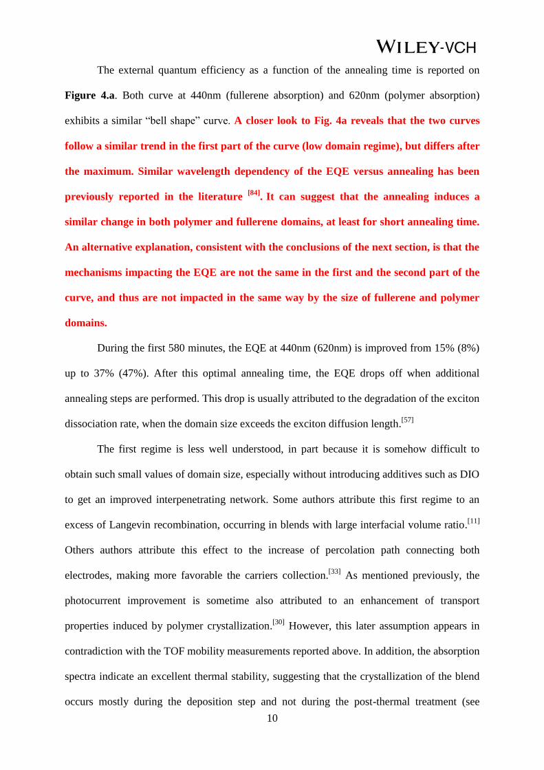
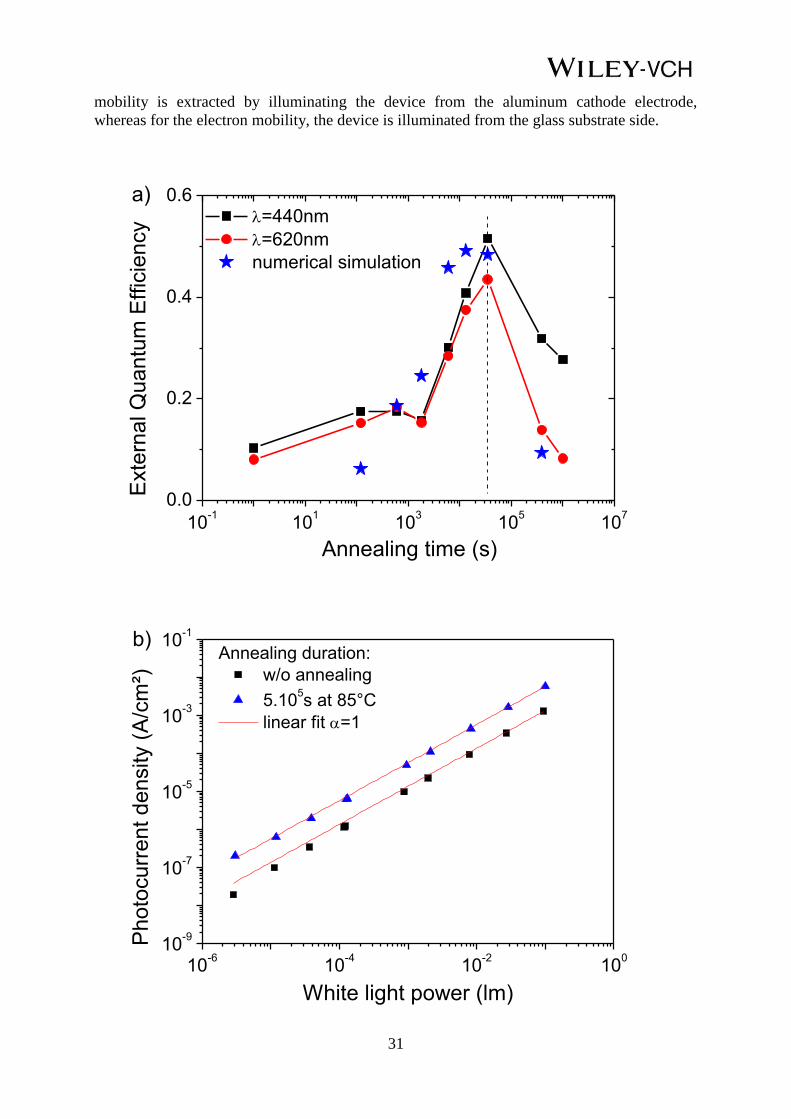
The external quantum efficiency as a function of the annealing time is reported on
Figure 4.a. Both curve at 440nm (fullerene absorption) and 620nm (polymer absorption)
exhibits a similar “bell shape” curve. A closer look to Fig. 4a reveals that the two curves
follow a similar trend in the first part of the curve (low domain regime), but differs after
the maximum. Similar wavelength dependency of the EQE versus annealing has been
previously reported in the literature [84]
. It can suggest that the annealing induces a
similar change in both polymer and fullerene domains, at least for short annealing time.
An alternative explanation, consistent with the conclusions of the next section, is that the
mechanisms impacting the EQE are not the same in the first and the second part of the
curve, and thus are not impacted in the same way by the size of fullerene and polymer
domains.
During the first 580 minutes, the EQE at 440nm (620nm) is improved from 15% (8%)
up to 37% (47%). After this optimal annealing time, the EQE drops off when additional
annealing steps are performed. This drop is usually attributed to the degradation of the exciton
dissociation rate, when the domain size exceeds the exciton diffusion length.[57]
The first regime is less well understood, in part because it is somehow difficult to
obtain such small values of domain size, especially without introducing additives such as DIO
to get an improved interpenetrating network. Some authors attribute this first regime to an
excess of Langevin recombination, occurring in blends with large interfacial volume ratio.[11]
Others authors attribute this effect to the increase of percolation path connecting both
electrodes, making more favorable the carriers collection.[33]
As mentioned previously, the
photocurrent improvement is sometime also attributed to an enhancement of transport
properties induced by polymer crystallization.[30]
However, this later assumption appears in
contradiction with the TOF mobility measurements reported above. In addition, the absorption
spectra indicate an excellent thermal stability, suggesting that the crystallization of the blend
occurs mostly during the deposition step and not during the post-thermal treatment (see
11
Figure S3). The use of additive such as DIO is most likely the cause of such stability. Our
interpretation will be discussed in the next section.
Photocurrent was measured as function of incident light flux in order to determine the
main recombination mechanism operating in the solar cell. Indeed, the dominant mechanism,
Langevin-type recombination versus trap assisted recombination, can be distinguished by
monitoring the slope of the photocurrent function of the incident light power. Langevin-type
recombination is known to be a second order mechanism, leading to nonlinear curves at high
light power, whereas trap assisted recombination is a first order mechanism, and thus does not
affect the linearity of photocurrent versus light flux curves.[43]
Results plotted in Figure 4.b do not show any non-linearity, suggesting that Langevin
recombination is not the dominant mechanism in these samples, at least for the range of light
flux investigated in this experiment. This point will be further investigated by simulation in
the final section. Moreover, both the dependence of the photocurrent with annealing duration,
and the poor value of quantum efficiency reported without initial annealing suggests that
recombination mechanisms are indeed present, mostly trap assisted recombination. This point
will be further confirmed by others experiments in the following section.
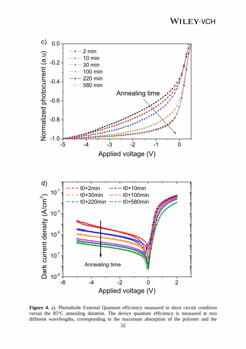
Normalized photocurrents versus applied voltage are plotted in Figure 4.c, for each
annealing step. The photocurrent normalization consists in dividing by the illuminated current
density value at -5V, according to:
5VI5VI
VIVII
darklight
adarkalight
norm
(2)
This procedure is performed in an attempt to simplify the visual comparison of each
curve. As in the EQE experiments, the voltage dependence of the current density improves
(i.e. reduced) with annealing time before reaching an optimal annealing point (580 minutes
annealing). Note that the built-in voltage seems almost unchanged during the successive steps,
suggesting that contact work functions are not affected by annealing.
12
Finally, the dark current is recorded for each annealing step (Figure 4.d). The dark
current density decreases continuously with annealing, scaling by more than 2 decades. Such
a trend has been reported in only few other works, presumably because the dark current is
typically not a figure of merit of solar cell devices.[58]
Moreover, optimized organic solar cell
have typically very thin active layers (~100nm), and consequently may suffer from additional
leakage current induced by pinholes. In some publications, the dependence of the dark current
on annealing has been attributed to the reduction of the shunt resistance, possibly burned out
by annealing[29]
or to a better contact selectivity, induced by changes in the vertical phase
composition profile.[59]
To summarize, current-voltage characteristics under dark and illumination show two
main trends: the improvement of the photocurrent dependence on the electric field, and the
drop in the reverse dark current.
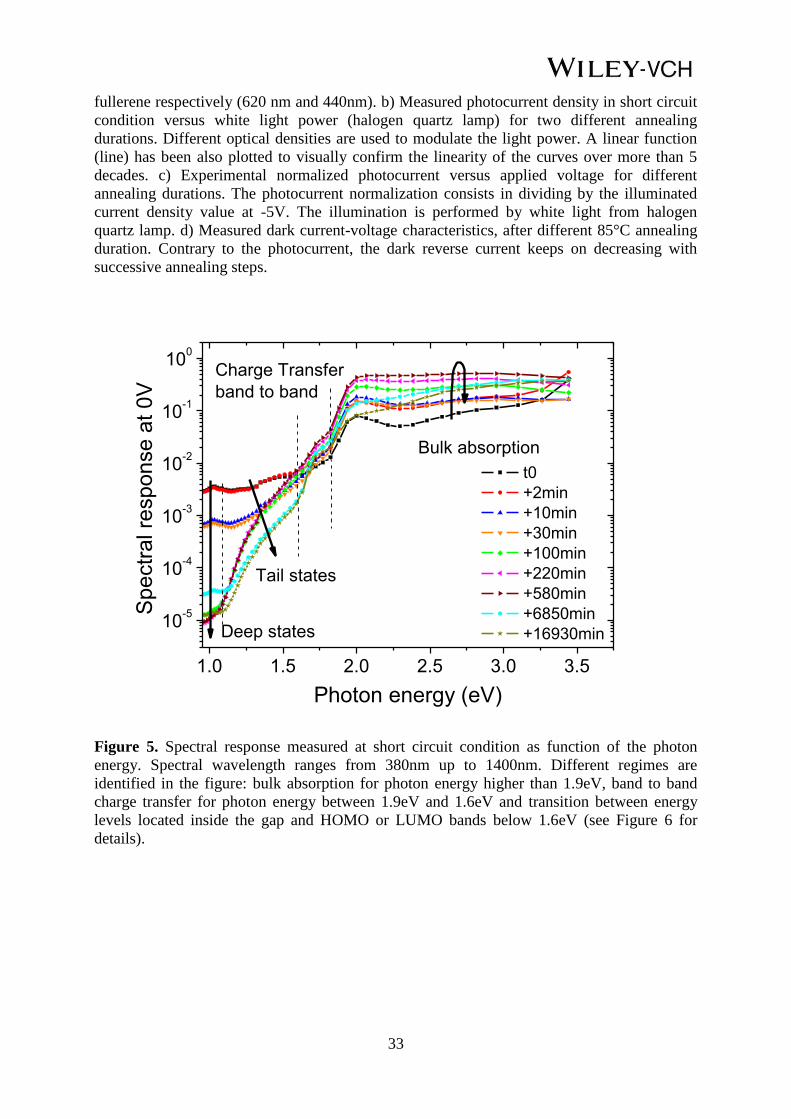
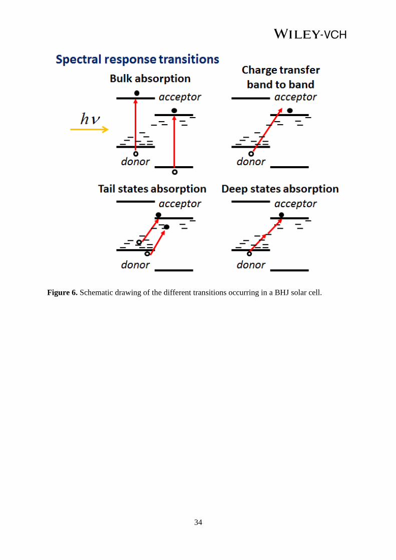
3.4. Infra-red EQE measurements
Following the work of Street et al., IR spectral response experiments were also
performed in order to probe the density of states in the energy gap.[40,42]
Regions of the
absorption curves corresponding to bulk absorption (transition from the HOMO to the LUMO
bands of the same semiconductor), charge transfer band-to-band across the donor/acceptor
interface, exponential absorption tail, and deep state charge transfer are indicated in Figure 5,
while the specifics of these transitions are represented in Figure 6. The optical band gap of
P3HT is 1.8eV whereas the optical band gap of the PC60BM is 2.4eV.
The most interesting part of the spectral response, below 1.6 eV in the regime of
charge transfer through gap states, exhibits a marked exponential dependence on photon
energy, consistent with an exponential density of states in the band tails. Furthermore, this
part of the spectral response is in large part reduced by annealing. The contribution from these
gap state-mediated transitions drops with the annealing time. To quantify this effect, a band
13
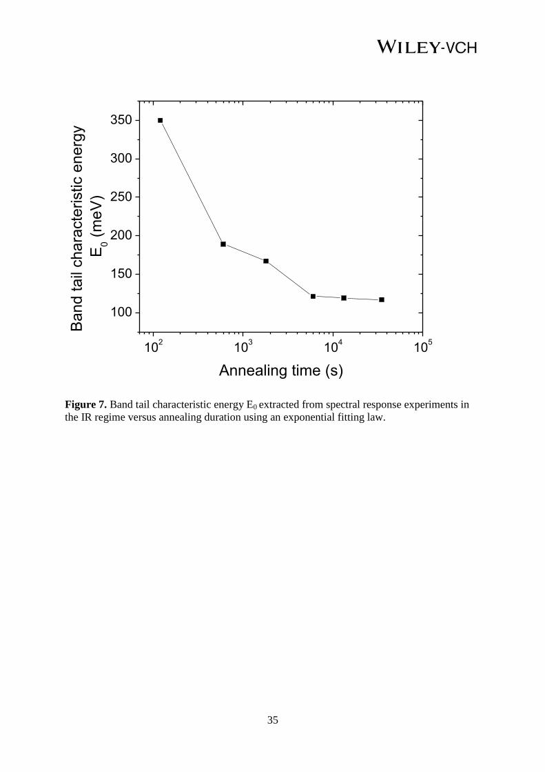
tail characteristic energy E0 is extracted using an exponential fit of the IR spectral response
experiment (discussed below, see Equation 5). The fitting procedure consists in fitting
every spectral response versus photon energy curves in the 1.1 eV - 1.5 eV range. As
shown in Figure 7, this characteristic energy E0 decreases with annealing time, which
indicates a drastic reduction of the density of trap states within the band gap of the blend layer.
3.5. Validation of the band tail characteristics energy extraction
As mentioned above, the characteristic energy extracted from EQE has been plotted on
Figure 7. EQE is only an indirect bulk measurement, which does not directly monitor the
density of states into the gap. Indeed, according to[60]
, the absorption coefficient (which is one
of the EQE component) for photon energy below the gap is related to the HOMO and LUMO
band tails density of states according the following formula (Equation 3):
dE hνEN EN hν
V Chνα
LUMO
E
EHOMO
FLUMO
HOMO
(3)
where VF is the heterojunction interface volume fraction and C a constant. The absorption
coefficient can be divided into a sum of three different contributions: band-to-band transition;
band-to-tail or tail-to-band transitions and tail-to-tail transition. Taking into account the
characteristic energy E0 of the respective HOMO and LUMO band tails, the density of states
into the gap are given by Equation 4 and Equation 5:
LUMOHOMO
0_H
HOMO
H_tail tailHOMO,EEE
E
EEexpNEN
(4)
LUMOHOMO
0_L
LUMO
L_tail tailLUMO,EEE
E
EEexpNEN
(5)
where NH_tail and NL_tail are the density of states at the tail band edge, E0_H/L band tail
characteristics energy of the HOMO and LUMO band tail population, and EHOMO the HOMO
energy, ELUMO the LUMO energy.
14
Computing Equation 3, for photon energy between Eg and Eg/2 (1.6eV and 0.8eV) the
band-to-tail absorption is found to be dominant over the tail-to-tail transition. In this case, the
absorption coefficient indeed exhibits a exp(hν/E0) dependence, where E0 is the highest band
tail characteristics energy between the HOMO and LUMO band. For photon energy below
Eg/2, Equation 3 shows that absorption only depends on tail-to-tail transition. In this regime,
again, an exp(hν/E0) dependence is found, with however a different E0 parameter (except if
identical band tail characteristics energy are assumed for both the HOMO and LUMO).
However, note that this regime of photon energy was not accessible in our experiments.
In conclusion, it is not possible to extract separately from spectral response
measurement both the value of the HOMO and LUMO band tail characteristic energy
E0_HOMO and E0_LUMO. Only the highest band tail characteristic energy is obtained where band-
to-tail or tail-to-band transitions are dominant over the other contributions.
4. Discussion
Let us summarize the experimental results reported in the previous section. The
dependence of I-V characteristics on annealing time both in illuminated and dark conditions
was measured. Results obtained show the existence of a preferred morphology in term of
short circuit current, together with constant improvement of the fill factor and decrease of the
dark current with annealing. Moreover, the blend morphology was characterized by
combining AFM and X-rays diffraction experiments, leading to an accurate description of the
P3HT domain evolution versus annealing. Electrons and holes mobilities were measured by
TOF experiments, indicating no significant evolution of the transport properties with
annealing duration.
The density of states in the gap of the materials was found to significantly depend on
annealing duration, as shown spectral response measurements.
15
In this section, experimental I-V curves obtained both in illuminated and dark
conditions are investigated using Drift and Diffusion simulations, carefully calibrated using
previously presented characterization results. In particular, the aim of this section is to
demonstrate that the dependence of the electrical response (both in dark and illuminated
conditions) on annealing is consistent with band tail DOS reorganization.
4.1. Drift diffusion simulations and calibration
The transport of electrons and holes into the blend is modelled using the extensively
used effective semiconductor approach proposed by Kostler et al.[61]
Simulations parameters
can be found in previous publications[62–65]
, and are reported in Table 1. Electron and hole
mobilities are modelled by field-dependent analytical expressions, obtained by fitting TOF
experiments. Both mobilities are taken independent of the annealing duration, in agreement
with experiments.
The polymer semiconductor is assumed to be intrinsic. In agreement with experiments,
the exponential band tail density of states is included, following the model proposed by
Urbach et al.[66]
and used in amorphous silicon photodiodes.[67]
For the sake of simplicity, the characteristics energy and band tails amplitude of both
HOMO and LUMO bands are assumed equal in the simulation. No additional deep traps are
implemented in the code. Trap assisted recombination and occupation probability of the tail
states are described by the Shockley-Read-Hall formalism (see Figure S4 for details).
Moreover, the HOMO-band-tail-states are assumed to be donor-like while the LUMO-band-
tail states are proposed to be acceptor-like[68]
: the charge induced by the possible ionisation of
these states is accounted into the self-consistent solution of the Poisson equation. Note that
trap-assisted recombinations are computed in this work without using any analytical
approximations, such as the popular Taylor and Simmons approximation.[69]
16
The blend morphology is taken into account in the simulation by adjusting both the
electron and holes generation and recombination terms. Following[70]
, the generation term is
modified to account for the poor exciton dissociation occurring in blend with too large P3HT
and PC60BM domains. Similarly, as electron and holes are supposed to recombine mostly at
the heterojunction interface, the recombination term is assumed propositional to the interface
volume fraction VF. Both terms depend on the P3HT average domain size <W>, which is
deduced from the AFM experiments.
Langevin recombination is also included in these simulations, using the well-known
(np-ni2) formula. Contrary to several previous works
[71,72], the Langevin prefactor is given
by its theoretical expression = e(µn+µp)/ε, which constitutes an upper estimation of the
Langevin recombination.
The resulting electron (hole) continuity equation is given by:
2
iFSRHF
ex
ex
nnnpγVRVG
2L
Wtanh
W
2LΦ
(6)
where n is the flux of electrons (holes), Lex the exciton diffusion length, G the optical
generation rate and RSRH the recombination rate defined from the SRH formalism.
4.2. Comparison between experimental photocurrent and simulations
Experimental photocurrents versus applied voltage curves are compared with simulation for
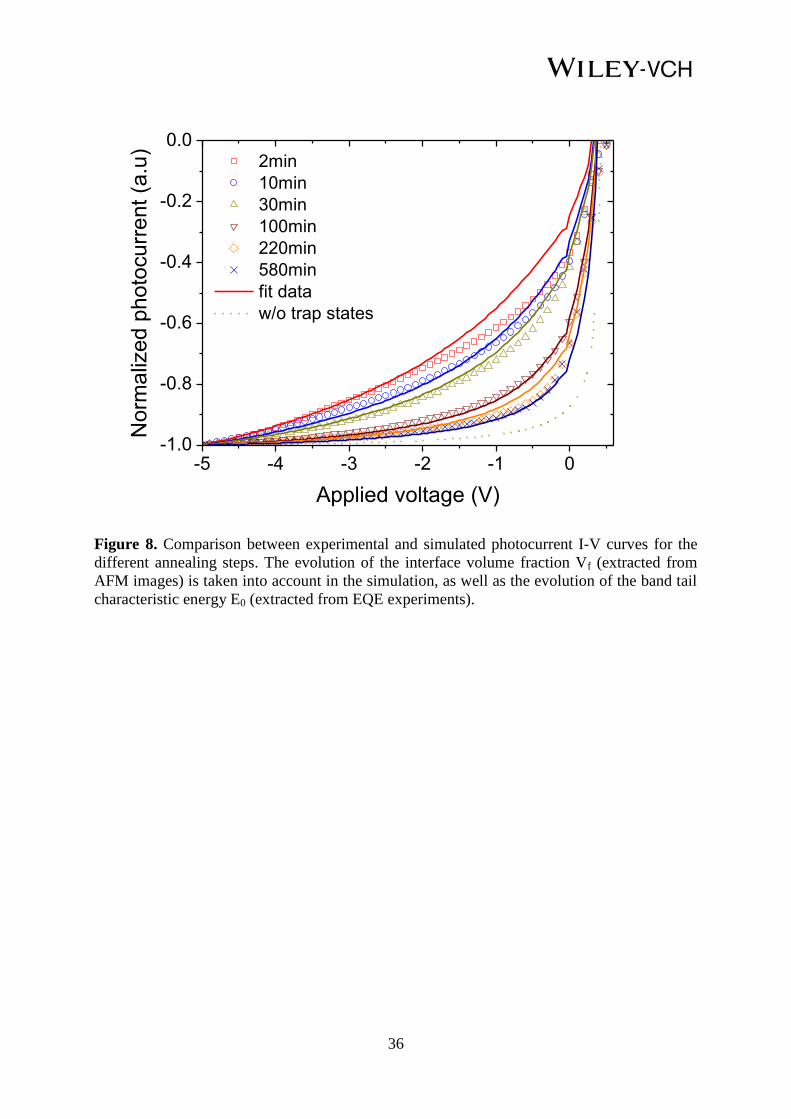
various annealing times. As seen in Figure 8, using the calibration explained for Figure 4.c,
all the data are nicely reproduced by the simulation. Note that only one single fitting
parameter is used here: the trap concentration at the band edge N0. This parameter is fixed at
the same value for the all the curves.
If the band tail characteristics energy E0 is arbitrary kept constant in the simulation, the
photocurrent field-dependence remains almost unchanged, despite the interface volume
fraction VF, underlying the critical impact of the band tail density of states on photocurrent.
17
Similarly, the spectral response under short circuit condition is simulated versus
annealing, and plotted together with experimental data on Figure 4.a. The simulation
parameters are the same as in Figure 8. Simulations qualitatively reproduce the “bell shape”
observed in the experiments, and confirm the interpretation of the two part of the curve:
exciton dissociation limited at large domain size, and trap assisted recombination at small
domain size.
Note that simulations have been performed for a different light power condition than
experiments. Indeed, the power used in simulation is 250 W/m2, instead of ~0.3 W/m2 in
experiments. This difference however do not impact the comparison, since the short circuit
current is indeed linearly dependent on the light power (as confirmed in experiments, see
Figure 4.b).
4.3. Non geminate Langevin versus SRH mechanism
As previously mentioned, recombinations in organic solar cells are usually attributed
to either Langevin or Shockley-Read Hall (SRH) mechanisms. The SRH recombination rate is
usually proportional to carrier density n, while the Langevin rate is proportional to the square
of the carrier density n2. For this reason, assuming standard value for the Langevin prefactor ,
this later mechanism typically dominates only at high light flux (> 1sun) in P3HT/PC60BM
blend [72]
or in forward bias beyond the built-in potential (OLED device).[73,74]
In the literature,
this point has been the source of debate.[40,75,76]
In practice, the dominant mechanism can be discriminated by measuring the linearity
of the photodiode current as function of light flux. Trap-assisted recombination keeps a linear
relation between the short circuit current density and the light intensity, whereas Langevin
type recombination induces nonlinear effects at high light flux (recombination term
proportional to the square of the carrier density).
18
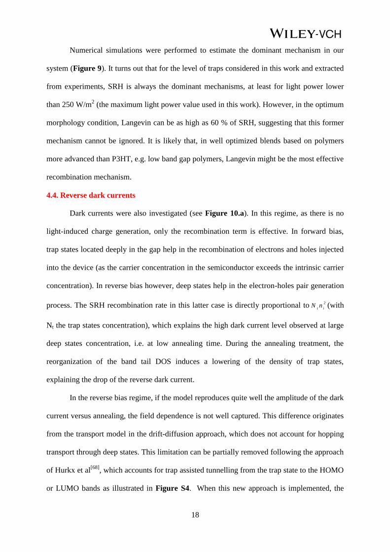
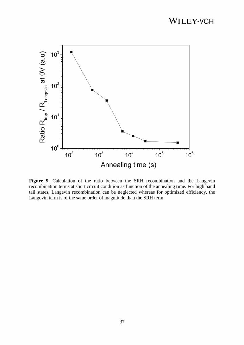
Numerical simulations were performed to estimate the dominant mechanism in our
system (Figure 9). It turns out that for the level of traps considered in this work and extracted
from experiments, SRH is always the dominant mechanisms, at least for light power lower
than 250 W/m2 (the maximum light power value used in this work). However, in the optimum
morphology condition, Langevin can be as high as 60 % of SRH, suggesting that this former
mechanism cannot be ignored. It is likely that, in well optimized blends based on polymers
more advanced than P3HT, e.g. low band gap polymers, Langevin might be the most effective
recombination mechanism.
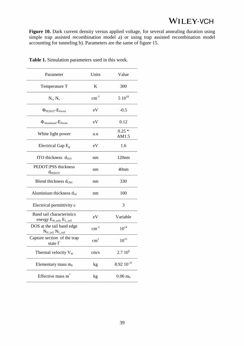
4.4. Reverse dark currents
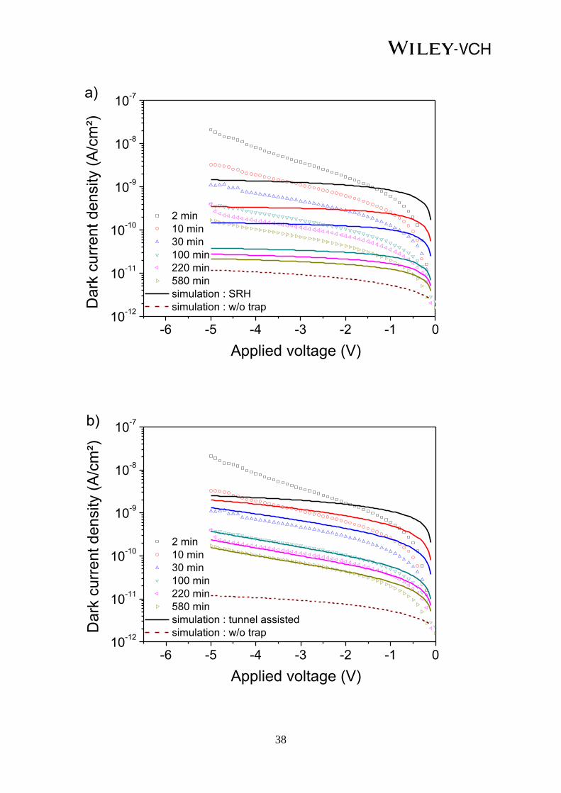
Dark currents were also investigated (see Figure 10.a). In this regime, as there is no
light-induced charge generation, only the recombination term is effective. In forward bias,
trap states located deeply in the gap help in the recombination of electrons and holes injected
into the device (as the carrier concentration in the semiconductor exceeds the intrinsic carrier
concentration). In reverse bias however, deep states help in the electron-holes pair generation
process. The SRH recombination rate in this latter case is directly proportional to2
itnN (with
Nt the trap states concentration), which explains the high dark current level observed at large
deep states concentration, i.e. at low annealing time. During the annealing treatment, the
reorganization of the band tail DOS induces a lowering of the density of trap states,
explaining the drop of the reverse dark current.
In the reverse bias regime, if the model reproduces quite well the amplitude of the dark
current versus annealing, the field dependence is not well captured. This difference originates
from the transport model in the drift-diffusion approach, which does not account for hopping
transport through deep states. This limitation can be partially removed following the approach
of Hurkx et al[68]
, which accounts for trap assisted tunnelling from the trap state to the HOMO
or LUMO bands as illustrated in Figure S4. When this new approach is implemented, the
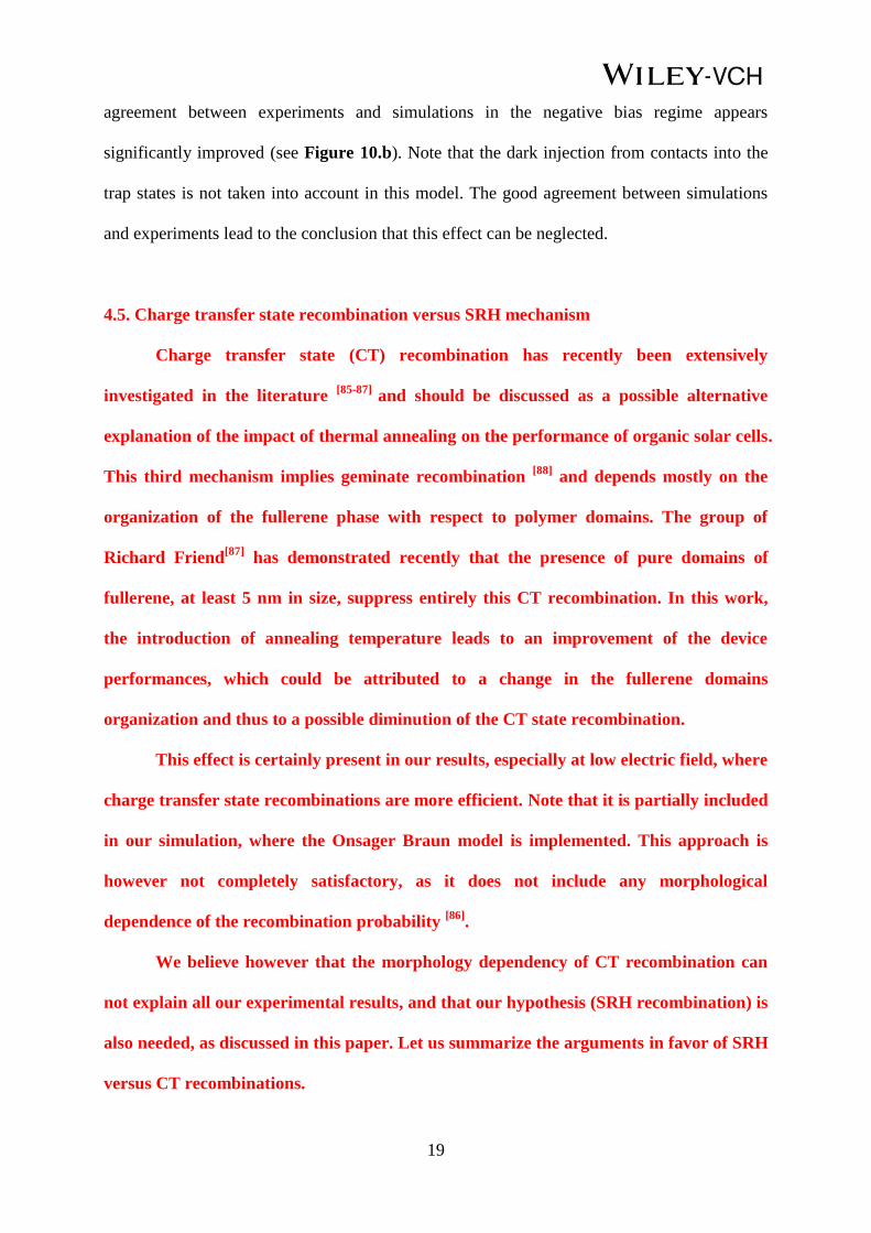
19
agreement between experiments and simulations in the negative bias regime appears
significantly improved (see Figure 10.b). Note that the dark injection from contacts into the
trap states is not taken into account in this model. The good agreement between simulations
and experiments lead to the conclusion that this effect can be neglected.
4.5. Charge transfer state recombination versus SRH mechanism
Charge transfer state (CT) recombination has recently been extensively
investigated in the literature [85-87]
and should be discussed as a possible alternative
explanation of the impact of thermal annealing on the performance of organic solar cells.
This third mechanism implies geminate recombination [88]
and depends mostly on the
organization of the fullerene phase with respect to polymer domains. The group of
Richard Friend[87]
has demonstrated recently that the presence of pure domains of
fullerene, at least 5 nm in size, suppress entirely this CT recombination. In this work,
the introduction of annealing temperature leads to an improvement of the device
performances, which could be attributed to a change in the fullerene domains
organization and thus to a possible diminution of the CT state recombination.
This effect is certainly present in our results, especially at low electric field, where
charge transfer state recombinations are more efficient. Note that it is partially included
in our simulation, where the Onsager Braun model is implemented. This approach is
however not completely satisfactory, as it does not include any morphological
dependence of the recombination probability [86]
.
We believe however that the morphology dependency of CT recombination can
not explain all our experimental results, and that our hypothesis (SRH recombination) is
also needed, as discussed in this paper. Let us summarize the arguments in favor of SRH
versus CT recombinations.
20
First of all, EQE experiments at low energy clearly indicate the presence of
shallow and deep traps into the gap, and allow quantifying the impact of thermal
annealing on their concentration. This effect is unlikely to be explained by pure CT
recombination. Moreover, our model, accounting only for the morphology dependency
of generation, non geminate langevin and SRH recombination, can nicely reproduced I-
V curves under illumination at all temperature annealing. There are no fitting
parameters in these simulations: mobility, domain size and traps concentrations have all
been extracted from complementary experiments (Time of Flight for mobility, AFM and
X-ray diffraction measurement for the domain size and EQE at low energy for the traps
concentration). Last but not least, the same model also explains, again without
additional fitting parameters, the impact of annealing on the dark currents, where
obviously CT recombinations are absent (no light). These conclusions, in the case of
P3HT/PCBM blends, are consistent with other works[88][89]
.
All these facts support the analysis presented here, if even more investigation is
needed to quantify more accurately the impact of CT recombinations.
The origin of the traps observed here through infra red EQE measurements is
not known. Different hypothesis are evoked in the literature. The band tail states may
originate from the polymer chain disorder inside the active layer[42][90]
, confirmed by
UPS measurement[91]
and by quantum chemistry simulations[92]
.
Defects can also induce traps, however not usually “band tails”. Localized traps
may originate from polymer chain scission[93]
or impurities such as oxygen[94]
or metallic
residues[95]
.
5. Conclusions
In this work, trap assisted recombinations have been investigated, focusing in
particular on the impact of thermal annealing durations in the classical P3HT:PC60BM solar
21
cells. Interestingly, while the spectral response versus annealing time exhibits a bell curve
with an optimum value, the dark currents however are monotonously reduced by annealing.
The second part of the spectral response (i.e decrease of the efficiency) is interpreted in term
of blend morphology change. Indeed AFM and X-rays diffraction measurements have
revealed that the growth of P3HT domains occurs in the 2D longitudinal directions. When the
average polymer domain width exceeds the exciton diffusion length, the solar cell efficiency
gets lower because of the exciton dissociation rate limitation.
On the other hand, this work demonstrates that the initial improvement of the spectral
response is not correlated to any carrier mobility improvement as confirmed by Time-of-
Flight experiments, where mobilities for both hole and electron have been extracted and found
unchanged during the annealing steps.
The impact of thermal annealing durations on the trap assisted recombination rate has
been investigated to explain both dark and light current changes. First, the existence of
exponential band tails into the gap has been experimentally confirmed by measuring the
device spectral response in the IR regime. Such method revealed the existence of large density
of states into the gap, largely reduced by the successive annealing steps.
All these results (mobility, bandtails) have then been used to calibrate Drift and
Diffusion simulations. It turns out that electrical and optical simulations can satisfactory
reproduce illuminated and dark experimental currents at the same time, versus voltage and
annealing time. These simulations highlight the predominance of the band tail states
reorganization in the improvement of the solar cell characteristics. Recombinations assisted
by trap states are lowered by annealing, which lead to an improvement of the solar cell
efficiency and a decrease of the reverse dark current (thermal generation from trap states).
This approach constitutes a powerful physical model, able to explain the existence of an ideal
morphology for photogenerated currents, and at the same time, able to capture the constant
reduction of dark current induced by annealing. An optimum in term of quantum efficiency is
22
found between the band tail states reorganization and the coarsening of the blend morphology
as function of thermal annealing duration.
6. Experimental Section
Opto-electrical characterization: Encapsulated devices were characterized in ambient air.
Opto-electrical measurements are performed on a dedicated optical bench. The devices are
placed in a light shielding box and can be illuminated by a specific optical head controlling
the size of the spot light on the device and insuring in-line measurement of the light power.
All light sources are placed outside of the shielding box and connected to the optical head by
a liquid light-guide.
Current-voltage (I-V) characteristics were measured with a Keithley 2636A in darkness and
under illumination (irradiance of 200 W/m²) obtained from a quartz tungsten halogen lamp
(LOT-Oriel 250W QTH light source).
For photodiode linearity measurement, the irradiance is reduced by insertion of different
optical densities. Photocurrents were recorded as function of incident light power.
For spectral response measurement, a 1/4m grating spectrometer (LOT-Oriel Cornerstone
130) with a resolution of 20 nm was used. The EQE measurements were performed at zero-
bias voltage to get the lowest dark current. The incident light power was measured with a
calibrated photodiodes: silicon sensor for wavelengths below 900 nm and an InGaAs sensor
up to 1.7µm .
AFM characterization: AFM phase measurements of the blend surface were performed in air
on specific separated samples using a Veeco Multimode AFM in tapping mode. AFM tips
(super sharp silicon tip purchased from NanoSensors) with 2 nm radius and resonance 300
kHz frequency were used in order to identify the different phases on fine blend morphology.
This insured clear distinction between crystalized and amorphous region on the blend surface.
23
The detector side of the AFM had an aluminum coating in order to improve the signal
detection.
Supporting Information Supporting Information is available from the Wiley Online Library or from the author.
Acknowledgements
The authors are grateful to Simon Charlot for photodiodes preparation and discussions
regarding solar cell fabrication. The work done at CEA was supported by ISORG. Work in
Princeton was supported in part by the National Science Foundation (DMR-1005892).
Received: ((will be filled in by the editorial staff))
Revised: ((will be filled in by the editorial staff))
Published online: ((will be filled in by the editorial staff))
[1] K. M. Coakley, M. D. McGehee, Chem. Mater. 2004, 16, 4533.
[2] J. Peet, M. L. Senatore, A. J. Heeger, G. C. Bazan, Adv. Mater. 2009, 21, 1521.
[3] M. A. Brady, G. M. Su, M. L. Chabinyc, Soft Matter 2011, 7, 11065.
[4] G. Li, R. Zhu, Y. Yang, Nat. Photonics 2012, 6, 153.
[5] C. W. Tang, Appl. Phys. Lett. 1986, 48, 183.
[6] NREL’s Best Research Cell Efficiencies as of Nov. 2013; 2013.
[7] G. Yu, J. Gao, J. Hummelen, F. Wudl, A.J. Heeger, Science 1995, 270, 1789.
[8] N. S. Sariciftci, L. Smilowitz, A. J. Heeger, F. Wudl, Science 1992, 258, 1474.
[9] J. J. M. Halls, K. Pichler, R. H. Friend, S. C. Moratti, A. B. Holmes, Appl. Phys. Lett. 1996, 68,
3120.
[10] J. K. J. van Duren, X. Yang, J. Loos, C. W. T. Bulle-Lieuwma, A. B. Sieval, J. C. Hummelen,
R. A. J. Janssen, Adv. Funct. Mater. 2004, 14, 425.
[11] P. K. Watkins, A. B. Walker, G. L. B. Verschoor, Nano Lett. 2005, 5, 1814.
[12] X. Yang, J. Loos, S. C. Veenstra, W. J. H. Verhees, M. M. Wienk, J. M. Kroon, M. A J.
Michels, R. A. J. Janssen, Nano Lett. 2005, 5, 579.
[13] M. Campoy-Quiles, T. Ferenczi, T. Agostinelli, P. G. Etchegoin, Y. Kim, T. D. Anthopoulos,
P. N. Stavrinou, D. D. C. Bradley, J. Nelson, Nat. Mater. 2008, 7, 158.
24
[14] H. Hoppe, N. Arnold, D. Meissner, N. S. Sariciftci, Thin Solid Films 2004, 451, 589.
[15] M. C. Heiber, A. Dhinojwala, J. Chem. Phys. 2012, 137, 014903.
[16] R. R. Lunt, J. B. Benziger, S. R. Forrest, Adv. Mater. 2010, 22, 1233.
[17] F. Yang, S. R. Forrest, ACS Nano 2008, 2, 1022.
[18] M. Dante, J. Peet, T.-Q. Nguyen, J. Phys. Chem. C 2008, 112, 7241.
[19] L. F. Drummy, R. J. Davis, D. L. Moore, M. Durstock, R. A. Vaia, J. W. P. Hsu, Chem. Mater.
2011, 23, 907.
[20] W. Ma, C. Yang, A. J. Heeger, Adv. Mater. 2007, 19, 1387.
[21] V. D. Mihailetchi, H. X. Xie, B. de Boer, L. J. A. Koster, P. W. M. Blom, Adv. Funct. Mater.
2006, 16, 699.
[22] Y. Kim, S. A. Choulis, J. Nelson, D. D. C. Bradley, S. Cook, J. R. Durrant, Appl. Phys. Lett.
2005, 86, 063502.
[23] J. Peet, J. Y. Kim, N. E. Coates, W. L. Ma, D. Moses, A. J. Heeger, G. C. Bazan, Nat. Mater.
2007, 6, 497.
[24] J. K. Lee, W. L. Ma, C. J. Brabec, J. Yuen, J. S. Moon, J. Y. Kim, K. Lee, G. C. Bazan, A. J.
Heeger, J. Am. Chem. Soc. 2008, 130, 3619.
[25] F. C. Krebs, Sol. Energy Mater. Sol. Cells 2009, 93, 394.
[26] C. N. Hoth, S. A. Choulis, P. Schilinsky, C. J. Brabec, Adv. Mater. 2007, 19, 3973.
[27] H. Hoppe, N. S. Sariciftci, J. Mater. Chem. 2006, 16, 45.
[28] C. Müller, T. A. M. Ferenczi, M. Campoy-Quiles, J. M. Frost, D. D. C. Bradley, P. Smith, N.
Stingelin-Stutzmann, J. Nelson, Adv. Mater. 2008, 20, 3510.
[29] F. Padinger, R. S. Rittberger, N. S. Sariciftci, Adv. Funct. Mater. 2003, 13, 85.
[30] T. Erb, U. Zhokhavets, G. Gobsch, S. Raleva, B. Stühn, P. Schilinsky, C. Waldauf, C. J.
Brabec, Adv. Funct. Mater. 2005, 15, 1193.
[31] L. H. Nguyen, H. Hoppe, T. Erb, S. Günes, G. Gobsch, N. S. Sariciftci, Adv. Funct. Mater.
2007, 17, 1071.
[32] U. Zhokhavets, T. Erb, H. Hoppe, G. Gobsch, N. S. Sariciftci, Thin Solid Films 2006, 496, 679.
[33] D. Chirvase, J. Parisi, J. C. Hummelen, V. Dyakonov, Nanotechnology 2004, 15, 1317.
[34] W. Ma, C. Yang, X. Gong, K. Lee, A. J. Heeger, Adv. Funct. Mater. 2005, 15, 1617.
[35] L. Zeng, C. W. Tang, S. H. Chen, Appl. Phys. Lett. 2010, 97, 053305.
[36] R. A. Marsh, C. Groves, N. C. Greenham, J. Appl. Phys. 2007, 101, 083509.
25
[37] L. Meng, D. Wang, Q. Li, Y. Yi, J.-L. Brédas, Z. Shuai, J. Chem. Phys. 2011, 134, 124102.
[38] B. Ray, M. A. Alam, Sol. Energy Mater. Sol. Cells 2012, 99, 204.
[39] L. J. A. Koster, O. Stenzel, S. D. Oosterhout, M. M. Wienk, V. Schmidt, R. A. J. Janssen,
2013, 3, 615.
[40] R. A. Street, M. Schoendorf, Phys. Rev. B 2010, 81, 1.
[41] R. A. Street, S. R. Cowan, A. J. Heeger, Phys. Rev. B 2010, 82, 11.
[42] R. A. Street, A. Krakaris, S. R. Cowan, Adv. Funct. Mater. 2012, 22, 4608.
[43] L. Dou, J. You, Z. Hong, Z. Xu, G. Li, R. A. Street, Y. Yang, Adv. Mater. 2013, 25, 6642.
[44] S. J. Lou, J. M. Szarko, T. Xu, L. Yu, T. J. Marks, L. X. Chen, J. Am. Chem. Soc. 2011, 133,
20661.
[45] S. Imamura, K. Palanisamy, S. Kannappan, S. Ochiai, J. Korean Phys. Soc. 2012, 61, 464.
[46] E. J. Spadafora, R. Demadrille, B. Ratier, B. Grévin, Nano Lett. 2010, 10, 3337.
[47] B. Ray, M. A. Alam, Appl. Phys. Lett. 2011, 99, 033303.
[48] H. Sirringhaus, P. Brown, R. Friend, Nature 1999, 401, 685.
[49] H. Scher, E. Montroll, Phys. Rev. B 1975, 12, 2455.
[50] S. Tiwari, N. C. Greenham, Opt. Quantum Electron. 2009, 41, 69.
[51] F. Monestier, J.-J. Simon, P. Torchio, L. Escoubas, F. Flory, S. Bailly, R. de Bettignies, S.
Guillerez, C. Defranoux, Sol. Energy Mater. Sol. Cells 2007, 91, 405.
[52] M. M. Mandoc, W. Veurman, J. Sweelssen, M. M. Koetse, P. W. M. Blom, Appl. Phys. Lett.
2007, 91, 073518.
[53] V. D. Mihailetchi, H. Xie, B. de Boer, L. M. Popescu, J. C. Hummelen, P. W. M. Blom, L. J.
A. Koster, Appl. Phys. Lett. 2006, 89, 012107.
[54] E. Couderc, N. Bruyant, A. Fiore, F. Chandezon, D. Djurado, P. Reiss, J. Faure-Vincent, Appl.
Phys. Lett. 2012, 101, 133301.
[55] V. Kažukauskas, M. Pranaitis, V. Čyras, L. Sicot, F. Kajzar, Thin Solid Films 2008, 516, 8988.
[56] H. Bassler, Phys. status solidi 1993, 175, 15.
[57] B. C. Thompson, J. M. J. Fréchet, Angew. Chem. Int. Ed. Engl. 2008, 47, 58.
[58] K.-J. Baeg, M. Binda, D. Natali, M. Caironi, Y.-Y. Noh, Adv. Mater. 2013, 25, 4267.
[59] T. Agostinelli, M. Campoy-Quiles, J. C. Blakesley, R. Speller, D. D. C. Bradley, J. Nelson,
Appl. Phys. Lett. 2008, 93, 203305.
26
[60] R. A. Street, K. Song, J. Northrup, S. R. Cowan, Phys. Rev. B 2011, 83, 1.
[61] L. J. A. Koster, E. Smits, V. D. Mihailetchi, P. W. M. Blom, Phys. Rev. B 2005, 72, 1.
[62] J. Cuiffi, T. Benanti, W. J. Nam, S. Fonash, Appl. Phys. Lett. 2010, 96, 143307.
[63] S. Altazin, R. Clerc, R. Gwoziecki, G. Pananakakis, G. Ghibaudo, C. Serbutoviez, Appl. Phys.
Lett. 2011, 99, 143301.
[64] J. Cao, Z. Zhan, L. Hou, Y. Long, P. Liu, W. Mai, Appl. Optics, 2012, 51, 5718.
[65] R. Hausermann, E. Knapp, M. Moos, N. A. Reinke, T. Flatz, B. Ruhstaller, J. Appl. Phys.
2009, 106, 104507.
[66] F. Urbach, Phys. Rev. 1953, 92, 1324.
[67] I. Sakata, Y. Hayashi, Appl. Phys. A 1985, 164, 153.
[68] N. R. Model, D. Simulation, I. Tunneling, G. A. M. Hurkx, D. B. M. Klaassen, M. P. G.
Knuvers, IEEE Trans. Electron Devices 1992, 39, 331.
[69] J. Simmons, G. Taylor, Phys. Rev. B 1971, 4, 502.
[70] B. Ray, M. A. Alam, Appl. Phys. Lett. 2011, 99, 033303.
[71] G.-J. A. H. Wetzelaer, N. J. Van der Kaap, L. J. A. Koster, P. W. M. Blom, Adv. Energy Mater.
2013, 3, 1130.
[72] M. Lenes, L. J. A. Koster, V. D. Mihailetchi, P. W. M. Blom, Appl. Phys. Lett. 2006, 88,
052104.
[73] G. A. H. Wetzelaer, M. Kuik, H. Nicolai, P. W. M. Blom, Phys. Rev. B 2011, 83, 165204.
[74] M. Kuik, L. J. A. Koster, A. G. Dijkstra, G. A. H. Wetzelaer, P. W. M. Blom, Org. Electron.
2012, 13, 969.
[75] C. Deibel, A. Wagenpfahl, Phys. Rev. B 2010, 82, 207301.
[76] R.A. Street, Phys. Rev. B 2010, 82, 207302.
[77] W. Yin, M. Dadmun, ACS Nano 2011, 5, 4756.
[78] D. Chen, A. Nakahara, D. Wei, D. Nordlund, T. P. Russell, Nano Lett. 2011, 11, 561.
[79] B. A. Collins, E. Gann, L. Guignard, X. He, C. R. McNeill, H. Ade, J. Phys. Chem. Lett. 2010,
1, 3160.
[80] N. D. Treat, M. A. Brady, G. Smith, M. F. Toney, E. J. Kramer, C. J. Hawker, M. L. Chabinyc,
Adv. Energy Mater. 2011, 1, 82.
[81] D. R. Kozub, K. Vakhshouri, L. M. Orme, C. Wang, A. Hexemer, E. D. Gomez,
Macromolecules 2011, 44, 5722.

27
[82] M. Pfannmöller, H. Flügge, G. Benner, I. Wacker, C. Sommer, M. Hanselmann, S. Schmale, H.
Schmidt, F. A. Hamprecht, T. Rabe, W. Kowalsky, R. R. Schröder, Nano Lett. 2011, 11, 3099.
[83] U. Vongsaysy, B. Pavageau, G. Wantz, D.M. Bassani, L. Servant, H. Aziz, Adv. Energy Mater.,
2014, 4, 3.
[84] L. Zeng, W.T. Ching, H.C. Shaw, Appl. Phys. Lett, 2010, 97,5.
[85] M. Hallermann, I. Kriegel, E. Da Como, J.M. Berger, E. Von Hauff, J. Feldmann Adv.
Funct. Mater. 2009, 19, 22.
[86] B. M. Savoie, A. Rao, A.A. Bakulin, S. Gelinas, B. Movaghar, R.H. Friend, T.J. Marks,
M.A. Ratner, JACS, 2014, 136, 7.
[87] S. Gélinas, A. Rao, A. Kumar, S.L. Smith, A.W. Chin, J. Clark, T.S. van der Poll, G.C.
Bazan, R.H. Friend, Science, 2014, 343, 6170.
[88] A.J. Heeger, Adv. Mater., 2014, 26, 1.
[89] R.A. Street, S.R. Cowan, A.J. Heeger, Phys. Rev. B, 2011, 83, 035205.
[90] Z.M. Beiley, h M., E.T. Hoke, R. Noriega, J. Dacuña, G.F. Burkhard, J.A. Bartelt, A.
Salleo, M.F. Toney, M.D. McGehee. Adv. Energy Mater., 2011, 1, 5.
[91] F. Bussolotti, S. Kera, K. Kudo, A. Kahn, N. Ueno, Phys. Rev. Lett., 2013 110, 26.
[92] J. Rivnay, R. Noriega, J. E. Northrup, R. J. Kline, M.F. Toney, A. Salleo, Phys. Rev.
B, 2011, 83, 12.
[93] R. A. Street, J. E. Northrup, B. S. Krusor, Phys. Rev. B, 2012, 85, 20.
[94] A. Seemann, H.J. Egelhaaf, C. J., Brabec, J.A. Hauch, Org. Elec., 2009, 10, 8.
[95] M.P. Nikiforov, B. Lai, W. Chen, S. Chen, R.D. Schaller, J. Strzalka, J. Maser, S. B.
Darling,. Energy and Environmental Science, 2013, 6, 5.
28
102
103
104
105
5
10
15
20
25
30
35
Extracted via AFM
best fit using:
Avera
ge
do
ma
in w
idth
<W
> (
nm
)
Annealing time (s)
<W>=<W0>+(Dt)n
<W0>=9.96nm
D=6.41*10-4 nm/s
n=1
Figure 1. Average domain width extracted from AFM images versus annealing time.
Symbols refer to experiments; line to a fitting obtained using the theoretical law proposed in
the work of [47]
.
29
100
101
102
103
104
105
5
10
15
20
Cohe
rence
leng
th (
nm
)
Annealing time (s)
b)
Figure 2. a). Schematic representation of the orientation of ordered P3HT domains with side
chains perpendicular to the substrate; b). Coherence length extracted from X-rays diffraction
spectra at the identified (001) peak using the Scherrer formula.
30
300 400 500 600 700 8000
2
4
6
8
Annealing time:
no annealing
10min
100min
600min
average
Ele
ctr
on
mo
bili
ty (
10
-4cm
²/V
s)
Square root of electric field (V/cm)0,5
a)
300 400 500 600 700 8000
2
4
6
8
b)
Annealing time:
no annealing
10min
100min
600min
average
Hole
mobili
ty (
10
-4cm
²/V
s)
Square root of electric field (V/cm)0,5
Figure 3. Electron (a) and Hole (b) mobility extracted from time-of-flight measurements, for
different annealing times, plotted against the square-root of the electric field. The hole
31
mobility is extracted by illuminating the device from the aluminum cathode electrode,
whereas for the electron mobility, the device is illuminated from the glass substrate side.
10-1
101
103
105
107
0.0
0.2
0.4
0.6 =440nm
=620nm
numerical simulation
Exte
rnal Q
uan
tum
Effic
iency
Annealing time (s)
a)
10-6
10-4
10-2
100
10-9
10-7
10-5
10-3
10-1
Annealing duration:
w/o annealing
5.105s at 85°C
linear fit =1
Ph
oto
cu
rre
nt
de
nsity (
A/c
m²)
White light power (lm)
b)
32
-5 -4 -3 -2 -1 0-1.0
-0.8
-0.6
-0.4
-0.2
0.0
Annealing time
2 min
10 min
30 min
100 min
220 min
580 min
Norm
aliz
ed p
hoto
curr
ent (a
.u)
Applied voltage (V)
c)
-6 -4 -2 0 210
-9
10-7
10-5
10-3
10-1
Annealing time
t0+2min t0+10min
t0+30min t0+100min
t0+220min t0+580min
Dark
curr
ent d
ensity (
A/c
m2)
Applied voltage (V)
d)
Figure 4. a). Photodiode External Quantum efficiency measured in short circuit condition
versus the 85°C annealing duration. The device quantum efficiency is measured at two
different wavelengths, corresponding to the maximum absorption of the polymer and the
33
fullerene respectively (620 nm and 440nm). b) Measured photocurrent density in short circuit
condition versus white light power (halogen quartz lamp) for two different annealing
durations. Different optical densities are used to modulate the light power. A linear function
(line) has been also plotted to visually confirm the linearity of the curves over more than 5
decades. c) Experimental normalized photocurrent versus applied voltage for different
annealing durations. The photocurrent normalization consists in dividing by the illuminated
current density value at -5V. The illumination is performed by white light from halogen
quartz lamp. d) Measured dark current-voltage characteristics, after different 85°C annealing
duration. Contrary to the photocurrent, the dark reverse current keeps on decreasing with
successive annealing steps.
1.0 1.5 2.0 2.5 3.0 3.5
10-5
10-4
10-3
10-2
10-1
100
Deep states
Tail states
Charge Transfer
band to band
Bulk absorption
t0
+2min
+10min
+30min
+100min
+220min
+580min
+6850min
+16930min
Spectr
al re
spon
se a
t 0V
Photon energy (eV)
Figure 5. Spectral response measured at short circuit condition as function of the photon
energy. Spectral wavelength ranges from 380nm up to 1400nm. Different regimes are
identified in the figure: bulk absorption for photon energy higher than 1.9eV, band to band
charge transfer for photon energy between 1.9eV and 1.6eV and transition between energy
levels located inside the gap and HOMO or LUMO bands below 1.6eV (see Figure 6 for
details).
34
Figure 6. Schematic drawing of the different transitions occurring in a BHJ solar cell.
35
102
103
104
105
100
150
200
250
300
350
Band
tail
cha
racte
ristic e
ne
rgy
E0 (
me
V)
Annealing time (s)
Figure 7. Band tail characteristic energy E0 extracted from spectral response experiments in
the IR regime versus annealing duration using an exponential fitting law.
36
-5 -4 -3 -2 -1 0-1.0
-0.8
-0.6
-0.4
-0.2
0.0 2min
10min
30min
100min
220min
580min
fit data
w/o trap states
Norm
aliz
ed p
hoto
curr
ent (a
.u)
Applied voltage (V)
Figure 8. Comparison between experimental and simulated photocurrent I-V curves for the
different annealing steps. The evolution of the interface volume fraction Vf (extracted from
AFM images) is taken into account in the simulation, as well as the evolution of the band tail
characteristic energy E0 (extracted from EQE experiments).
37
102
103
104
105
106
100
101
102
103
R
atio R
tra
p /
RL
an
ge
vin a
t 0V
(a.u
)
Annealing time (s)
Figure 9. Calculation of the ratio between the SRH recombination and the Langevin
recombination terms at short circuit condition as function of the annealing time. For high band
tail states, Langevin recombination can be neglected whereas for optimized efficiency, the
Langevin term is of the same order of magnitude than the SRH term.
38
-6 -5 -4 -3 -2 -1 010
-12
10-11
10-10
10-9
10-8
10-7a)
2 min
10 min
30 min
100 min
220 min
580 min
simulation : SRH
simulation : w/o trapDark
curr
ent d
ensity (
A/c
m²)
Applied voltage (V)
-6 -5 -4 -3 -2 -1 010
-12
10-11
10-10
10-9
10-8
10-7
2 min
10 min
30 min
100 min
220 min
580 min
simulation : tunnel assisted
simulation : w/o trapDa
rk c
urr
en
t d
en
sity (
A/c
m²)
Applied voltage (V)
b)
39
Figure 10. Dark current density versus applied voltage, for several annealing duration using
simple trap assisted recombination model a) or using trap assisted recombination model
accounting for tunneling b). Parameters are the same of figure 15.
Table 1. Simulation parameters used in this work.
Parameter Units Value
Temperature T K 300
Nc, Nv cm-3
5 1018
ΦPEDOT-EFermi eV -0.5
ΦAluminum-EFermi eV 0.12
White light power a.u 0.25 *
AM1.5
Electrical Gap Eg eV 1.6
ITO thickness dITO nm 120nm
PEDOT:PSS thickness
dPEDOT
nm 40nm
Blend thickness dOSC nm 330
Aluminium thickness dAl nm 100
Electrical permittivity 3
Band tail characteristics
energy EH_tail, EL_tail
eV Variable
DOS at the tail band edge
NH_tail, NL_tail cm
-3 10
14
Capture section of the trap
state cm
2 10
15
Thermal velocity Vth cm/s 2.7 106
Elementary mass m0 kg 8.92 10-31
Effective mass m*
kg 0.06 m0
40
Copyright WILEY-VCH Verlag GmbH & Co. KGaA, 69469 Weinheim, Germany, 2013.
Supporting Information
Title: Impact of blend morphology on interface state recombinations in bulk heterojunction
organic solar cells
Author(s), and Corresponding Author(s)*: Benjamin Bouthinon*, Raphaël Clerc, Jerôme
Vaillant, Jean Marie Verilhac, Jérôme Faure-Vincent, David Djurado, Irina Ionica, Gabriel
Man, Antoine Gras, Georges Pananakakis, Romain Gwoziecki, Antoine Kahn.
((Optional Dedication))
Figure S1. Atomic Force Microscope (AFM) phase measurement in tapping mode performed
on the P3HT:PC60BM blend surface, obtained with different annealing duration (2min, 60min,
100min and 580min). The blend layer was spin coated on the ITO coated glass substrate.
41
4.0 4.5 5.0 5.5 6.0 6.5 7.0 7.5 8.00.0
2.5
5.0
Norm
aliz
ed inte
nsity
(°)
2 = 6.1907°
d = 16.56 إ
= 0.8907°
= 104 إ
W/O annealing
10 20 30 40 50 601.0
1.5
2.0
2.5
3.0
3.5
(°)
W/O annealing
Norm
aliz
ed inte
nsity
200
300
4.0 4.5 5.0 5.5 6.0 6.5 7.0 7.5 8.00
2
4
6
Norm
aliz
ed inte
nsity
(°)
Annealing time 10min 85°C
2 = 6.2685°
d = 16.36 إ
= 0.6765°
= 137 إ
10 20 30 40 50 601.0
1.2
1.4
1.6
1.8
2.0
2.2
2.4
(°)
Annealing time 10min 85°C
Norm
aliz
ed inte
nsity
200
300
4.0 4.5 5.0 5.5 6.0 6.5 7.0 7.5 8.00
2
4
6
Annealing time 100min 85°C
Norm
aliz
ed inte
nsity
(°)
2 = 6.1632°
d = 16.639 إ
= 0.6937°
= 133 إ
10 20 30 40 50 601.00
1.25
1.50
1.75
2.00
(°)
Annealing time 100min 85°C
Norm
aliz
ed inte
nsity
200
300
4.0 4.5 5.0 5.5 6.0 6.5 7.0 7.5 8.00
2
4
6
Annealing time 580min 85°C
Norm
aliz
ed inte
nsity
(°)
2 = 6.1783°
d = 16.60 إ
= 0.6690°
= 138 إ
10 20 30 40 50 601.0
1.5
2.0
2.5
(°)
Annealing time 580min 85°C
Norm
aliz
ed inte
nsity
200
300
Figure S2. XRD spectra for the different annealing step. (100), (200) and (300) are identified
on every spectrum. The coherence length on the (100) peak is extracted using the Scherrer
formula.
42
300 400 500 600 700 800
Absorp
tion
(a.u
)
Wavelength (nm)
Annealing time :
0 s
102 s
104 s
Figure S3. Absorption spectra of P3HT:PC60BM blend layer with 95% of CB and 5% of DIO.
The crystallization order of the film is unchanged along with the annealing.
Langevin recombination is described by the following formalism:
2
02
i
he
r
Lnnp
µµqR
(1)
With ni the intrinsic carrier concentration, µe/h the carrier mobility, q the elementary charge, r
the dielectric constant of the polymer and , 0 the dielectric constant in the vacuum.
The recombination rate in the Shockley Read Hall formalism is given by the following
relation:
t
p
t
n
ii
tSRH
ppC
nnC
pnnpNR
11 (2)
With Nt the trap density of states, Cp and Cn the capture cross section of the trap states taken
as equal (Taylor and Simmons approximation). The electron nt and hole pt trapped density
are defined by:
Tk
EENn
B
Lt
Ctexp (3)
43
Tk
EENp
B
Ht
Vtexp (4)
With Et the energy trap depth with respect to the band edge.
The probability of occupation of the trap level at the energy Et is given by:
tt
t
ppnn
pnEf
(5)
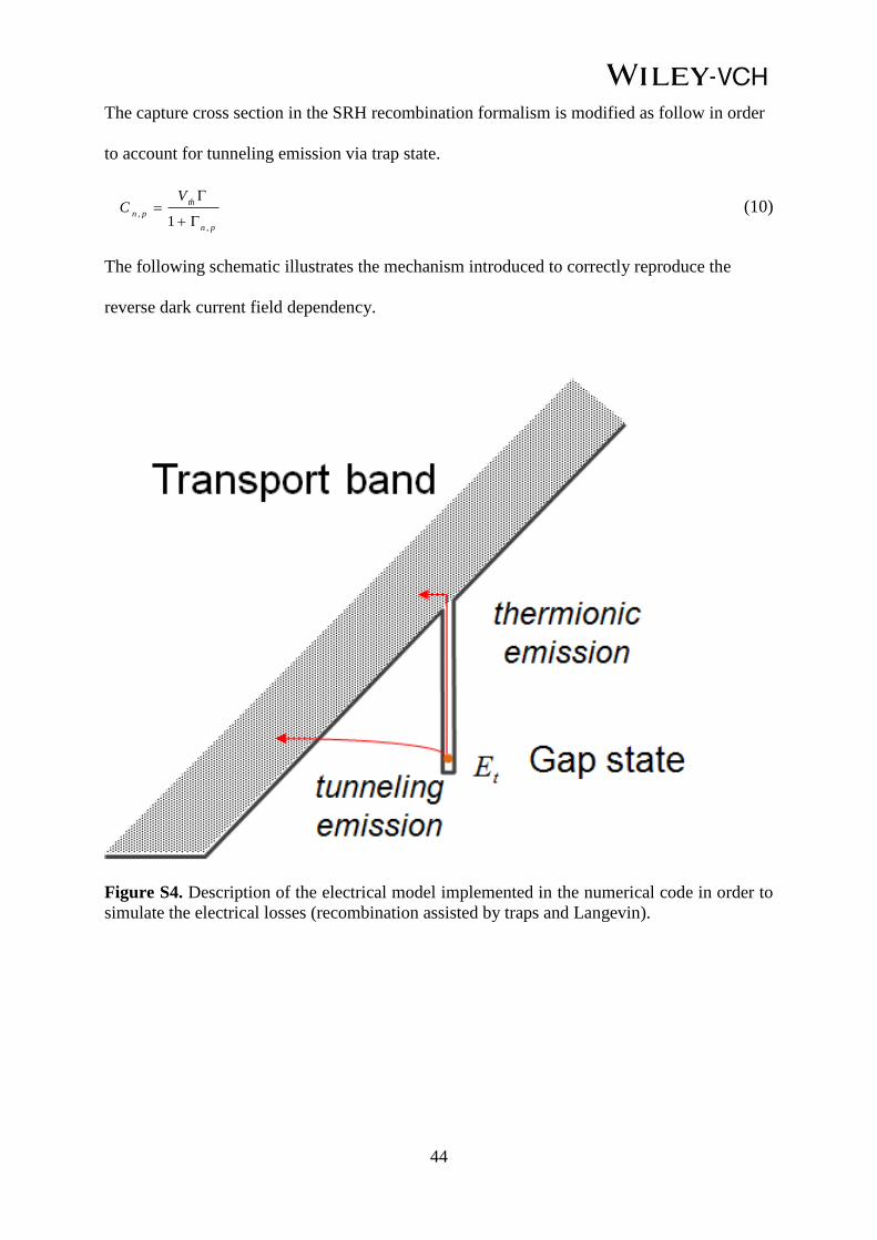
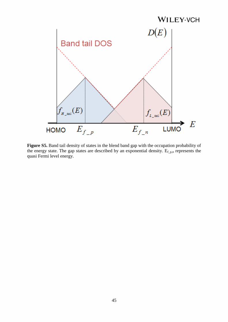
Exponential band tail states distribution are implemented for both the HOMO and the LUMO
in agreement with the experiments:
LUMOHOMO
0_H
HOMO
H_tail tailHOMO,EEE
E
EEexpNEN
(6)
LUMOHOMO
0_L
LUMO
L_tail tailLUMO,EEE
E
EEexpNEN
(7)
where NH_tail and NL_tail are the density of states at the tail band edge, E0_H/L band tail
characteristics energy of the HOMO and LUMO band tail population, and EHOMO the HOMO
energy, ELUMO the LUMO energy.
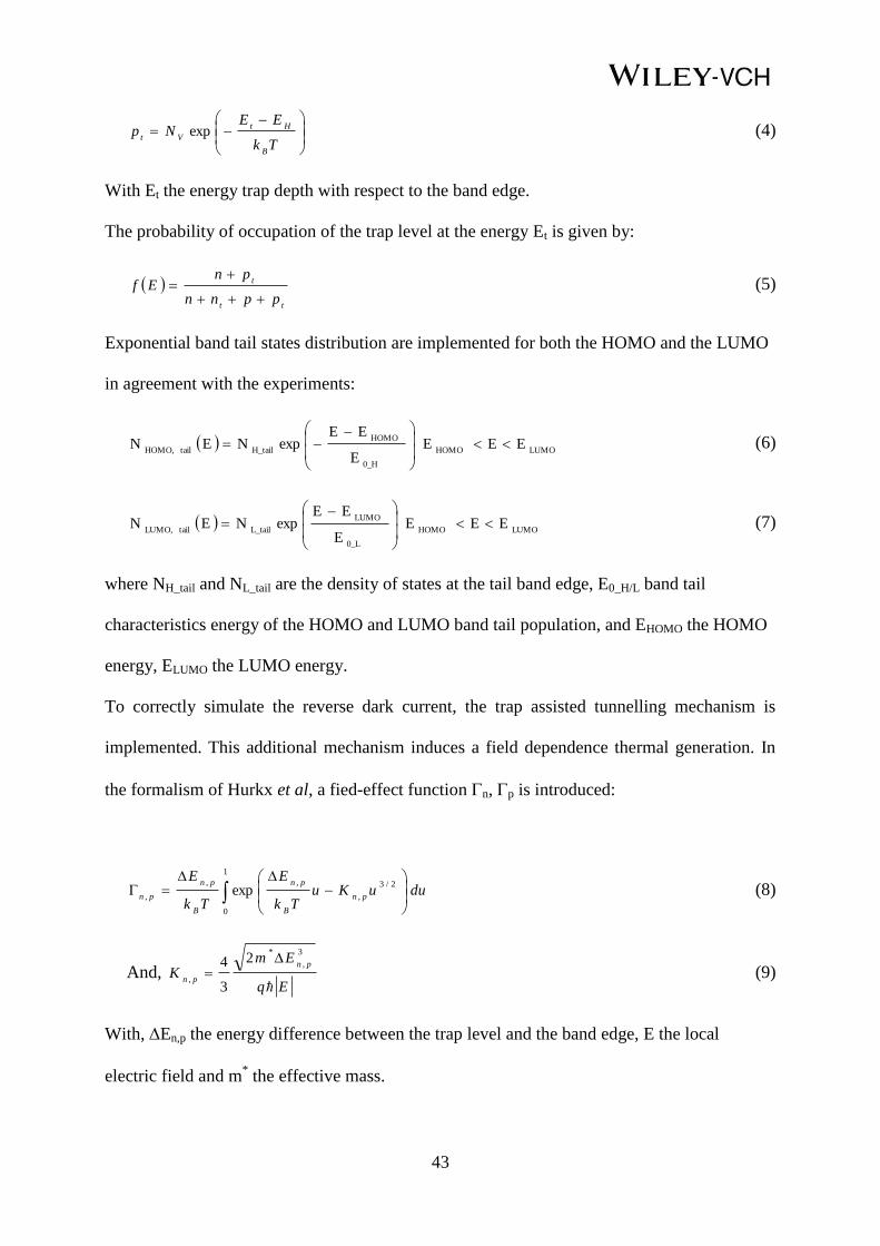
To correctly simulate the reverse dark current, the trap assisted tunnelling mechanism is
implemented. This additional mechanism induces a field dependence thermal generation. In
the formalism of Hurkx et al, a fied-effect function n, p is introduced:
1
0
2/3
,
,,
, exp duuKu
Tk
E
Tk
E
pn
B
pn
B
pn
pn (8)
And, Eq
EmK
pn
pn
3
,
*
,
2
3
4 (9)
With, En,p the energy difference between the trap level and the band edge, E the local
electric field and m* the effective mass.
44
The capture cross section in the SRH recombination formalism is modified as follow in order
to account for tunneling emission via trap state.
pn
th
pn
VC
,
,1
(10)
The following schematic illustrates the mechanism introduced to correctly reproduce the
reverse dark current field dependency.
Figure S4. Description of the electrical model implemented in the numerical code in order to
simulate the electrical losses (recombination assisted by traps and Langevin).
45
Figure S5. Band tail density of states in the blend band gap with the occupation probability of
the energy state. The gap states are described by an exponential density. Ef_p,n represents the
quasi Fermi level energy.