Embed Size (px)
Citation preview
JOURNAL OF SEMICONDUCTOR TECHNOLOGY AND SCIENCE, VOL.16, NO.2, APRIL, 2016 ISSN(Print) 1598-1657 http://dx.doi.org/10.5573/JSTS.2016.16.2.185 ISSN(Online) 2233-4866
Manuscript received Sep. 22, 2016; accepted Jan. 28, 2016 This work was supported by the National Research Foundation of Korea (NRF) grant funded by the Korea government (MSIP) (No. 2014R1A2A1A11050637). Also, this work was supported by IDEC (EDA Tool, MPW). H. Lee and K. Cho are co-first author. 1 Inter-universitty Semiconductor Research Center (ISRC) and School of Electrical and Computer Engineering, Seoul National University, Korea 2 School of Electrical and Computer Engineering, University of Seoul, Korea E-mail : [email protected] (Corresponding author)
Impact of Trap Position on Random Telegraph Noise in a 70-Å Nanowire Field-Effect Transistor
Hyunseul Lee1, Karam Cho2, Changhwan Shin2,*, and Hyungcheol Shin1
Abstract—A 70-Å nanowire field-effect transistor (FET) for sub-10-nm CMOS technology is designed and simulated in order to investigate the impact of an oxide trap on random telegraph noise (RTN) in the device. It is observed that the drain current fluctuation (ΔID/ID) increases up to a maximum of 78 % due to the single electron trapping. In addition, the effect of various trap positions on the RTN in the nanowire FET is thoroughly analyzed at various drain and gate voltages. As the drain voltage increases, the peak point for the ΔID/ID shifts toward the source side. The distortion in the electron carrier density and the conduction band energy when the trap is filled with an electron at various positions in the device supports these results. Index Terms—Nanowire field-effect transistor, random telegraph noise, TCAD
I. INTRODUCTION
As the feature size of the modern field-effect transistors (FETs) is scaled down below 10 nm, the short channel effect in the electron devices is one of the most difficult technical challenges. As the critical dimensions
shrink to a few nanometers, non-conventional device structures that can successfully suppress the short channel effect have been proposed. For example, double-gate FinFET [1, 2], Fully-Depleted Silicon-on-Insulator (FD-SOI) MOSFET [3, 4], and gate-all-around (GAA) MOSFET [5-10] have attracted much attention in the industry. Among them, the nanowire FET has the highest gate-to-channel capacitive coupling primarily because the channel is surrounded and controlled by the gate in all directions, and therefore, silicon nanowire architecture is the most attractive structure for sub-10-nm CMOS technology.
Because even the extremely scaled sub-10-nm device has several defects, random telegraph noise (RTN) created by an oxide trap plays an important role in analyzing device performance [11-13]. The sub-10-nm nanowire FET should be designed considering the impact of oxide traps on its performance. However, there is currently no study on the impact of RTN created by a single-trap in a 70-Å nanowire FET, to the best of authors’ knowledge. In this work, the critical effect of a single trap on the performance variation of a 70-Å nanowire FET is discussed in detail, and the impact of various oxide trap positions on the drain current fluctuation is quantitatively analyzed.
II. NANOWIRE FET DESIGN AND SIMULATION
APPROACH
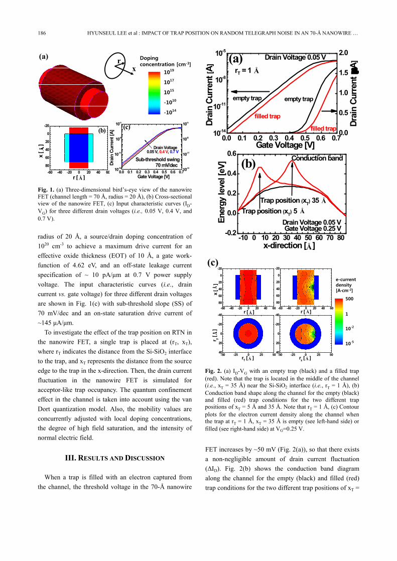
Based on the international technology roadmap for semiconductor (ITRS), the nanowire FET design (Fig. 1(a) and (b)) for low-power sub-10-nm technology is optimized using three-dimensional (3-D) device simulations by selecting a channel length of 70 Å, a
186 HYUNSEUL LEE et al : IMPACT OF TRAP POSITION ON RANDOM TELEGRAPH NOISE IN AN 70-Å NANOWIRE …
radius of 20 Å, a source/drain doping concentration of 1020 cm-3 to achieve a maximum drive current for an effective oxide thickness (EOT) of 10 Å, a gate work-function of 4.62 eV, and an off-state leakage current specification of ~ 10 pA/μm at 0.7 V power supply voltage. The input characteristic curves (i.e., drain current vs. gate voltage) for three different drain voltages are shown in Fig. 1(c) with sub-threshold slope (SS) of 70 mV/dec and an on-state saturation drive current of ~145 μA/μm.
To investigate the effect of the trap position on RTN in the nanowire FET, a single trap is placed at (rT, xT), where rT indicates the distance from the Si-SiO2 interface to the trap, and xT represents the distance from the source edge to the trap in the x-direction. Then, the drain current fluctuation in the nanowire FET is simulated for acceptor-like trap occupancy. The quantum confinement effect in the channel is taken into account using the van Dort quantization model. Also, the mobility values are concurrently adjusted with local doping concentrations, the degree of high field saturation, and the intensity of normal electric field.
III. RESULTS AND DISCUSSION
When a trap is filled with an electron captured from the channel, the threshold voltage in the 70-Å nanowire
FET increases by ~50 mV (Fig. 2(a)), so that there exists a non-negligible amount of drain current fluctuation (ΔID). Fig. 2(b) shows the conduction band diagram along the channel for the empty (black) and filled (red) trap conditions for the two different trap positions of xT =
0.0 0.1 0.2 0.3 0.4 0.5 0.6 0.710-14
10-11
10-8
10-5
Drai
n Cu
rrent
[mA]
empty trap
filled trap
Gate Voltage [V]
Drai
n Cu
rrent
[A]
rT = 1
Drain Voltage 0.05 V
Å
filled trap
empty trap
0.0
0.5
1.0
1.5
2.0
(a)
-10 0 10 20 30 40 50 60 70 80-0.2
0.0
0.2
0.4
0.6
Gate Voltage 0.25 VDrain Voltage 0.05 V
ÅÅ
Å
Trap position (xT) 5
Conduction band
Trap position (xT) 35
Ener
gy le
vel [
eV]
x-direction [ ]
(b)
-60 -40 -20 0 20 40 6080
60
40
20
0
-20
Å
x [
]
r [ ]-60 -40 -20 0 20 40 60
80
60
40
20
0
-20
ÅÅ
r [ ]
(c)
-50 -25 0 25 5040
20
0
-20
-40
r y [
]
ÅrT [ ]-50 -25 0 25 5040
20
0
-20
-40
Årz [ ]
e-current density [A·cm-2]
500
1
10-2
10-5
Fig. 2. (a) ID-VG with an empty trap (black) and a filled trap (red). Note that the trap is located in the middle of the channel (i.e., xT = 35 Å) near the Si-SiO2 interface (i.e., rT = 1 Å), (b) Conduction band shape along the channel for the empty (black) and filled (red) trap conditions for the two different trap positions of xT = 5 Å and 35 Å. Note that rT = 1 Å, (c) Contour plots for the electron current density along the channel when the trap at rT = 1 Å, xT = 35 Å is empty (see left-hand side) or filled (see right-hand side) at VG=0.25 V.
rx
(a) Doping concentration [cm-3]
1019
1017
1015
-1010
-1014
-60 -40 -20 0 20 40 6080
60
40
20
0
-20
x [
]
Å
r [ ]
(b)
0.0 0.1 0.2 0.3 0.4 0.5 0.6 0.710-14
10-11
10-8
10-5
10-14
10-11
10-8
10-5
Drain Voltage
Drai
n Cu
rren
t [A]
Gate Voltage [V]
Sub-threshold swing 70 mV/dec
(c)
0.05 V, 0.4 V, 0.7 V
Fig. 1. (a) Three-dimensional bird’s-eye view of the nanowire FET (channel length = 70 Å, radius = 20 Å), (b) Cross-sectional view of the nanowire FET, (c) Input characteristic curves (ID-VG) for three different drain voltages (i.e., 0.05 V, 0.4 V, and 0.7 V).

JOURNAL OF SEMICONDUCTOR TECHNOLOGY AND SCIENCE, VOL.16, NO.2, APRIL, 2016 187
5 Å and 35 Å (rT = 1 Å). The single electron captured at the trap significantly raises the conduction band energy level (see the two red-colored curves in Fig. 2(b)) by ~0.2 eV. The impact of the single trap, filled with the captured electron, on the electron current density is clearly depicted in Fig. 2(c). The two contour plots on the left-hand side in Fig. 2(c) show the electron current density with the empty trap site in the r-x (upper) and ry-rz (lower) planes. On the right-hand side, the two contour plots show the electron current density with the filled trap site. When present, the single trap should significantly affect the drain current in the channel. Quantitatively, ΔID/ID is ~78%, as shown in Fig. 3(a).
To investigate the effect of the trap position on the drain current, rT is first varied from 1 Å to 9 Å for xT = 35 Å. As shown in Fig. 3(a), the drain current varies between 13 % and 78% at VG = 0.05 V. The performance variation in the 70-Å nanowire FET intensifies when the
trap is close to the channel. The proximity of the trap to the Si-SiO2 interface significantly distorts the channel potential, resulting in the local variation of the current density (Fig. 3(b)). As is also shown in Fig. 3(a), the amplitude of RTN (i.e., the drain current fluctuation) becomes large when the nanowire FET operates in the sub-threshold region. This increase indicates that the channel potential is more sensitive to the trap because the gate-to-channel controllability is relatively smaller in the sub-threshold region.
Fig. 4(a) shows the effect of trap position along the channel (i.e., in the x-direction from the source to the drain) on the drain current fluctuation at a drain voltage of 0.05 V with the trap located near the Si-SiO2 interface at 1 Å (i.e., rT = 1 Å). Interestingly, ΔID/ID for xT = 5 Å and 65 Å (or 15 Å and 55 Å, or 25 Å and 45 Å) are almost same because of the symmetric conduction band in the channel (black-colored line in Fig. 4(b)). However, as the drain voltage increases, the conduction band diagram becomes asymmetric (i.e., the conduction band edge is lower on the drain side than on the source side), and therefore, the peak point for ΔID/ID is shifted toward the source side (Fig. 4(c)). Moreover, conduction band distortion due to the proximity of the trap to the source side (vs. the trap in the middle of the channel) occurs when the gate voltage increases from 0.25 V to 0.7 V (Fig. 4(b) and (d)). Hence, the impact of the trap position near the source and the Si-SiO2 interface would be the most significant when the nanowire FET is operating in saturation mode.
IV. CONCLUSIONS
The effect of a single trap on the device performance in a 70-Å silicon nanowire FET has been investigated using 3-D TCAD simulations. The impact of the position of the trap on the drain current fluctuation has been quantitatively analyzed. The highest drain current variation (i.e., ΔID/ID ~ 78%) was observed when the trap was placed near the source side and close to Si-SiO2 interface. Finally, the peak point for the ΔID/ID was shown to shift from the middle of the channel toward the source side with an increase in the drain voltage.
0.0 0.1 0.2 0.3 0.4 0.5 0.6 0.70102030405060708090
0102030405060708090
rT = 1 Å
DId/I
d [%
]
Gate Voltage [V]
Drain Voltage 0.05 V
rT = 9 Å
(a)
(b)1 Å 3Å 5Å Å 9Å7
Fig. 3. (a) ΔID/ID vs. VG with rT = 1 Å to 9 Å in increments of 1 Å for xT = 35 Å, (b) Contour plot for the current density with rT= 1 Å to 9 Å in increments of 2 Å. Note that a lower current density flows near the trap (rT, xT) = (1 Å, 35 Å) because of increased distortion in the channel potential by the single filled trap resulting in a locally high threshold voltage.

188 HYUNSEUL LEE et al : IMPACT OF TRAP POSITION ON RANDOM TELEGRAPH NOISE IN AN 70-Å NANOWIRE …
REFERENCES
[1] D. Hisamoto, W.-C. Lee, J. Kedzierski, H. Takeuchi, K. Asano, C. Kuo, E. Anderson, T.-J. King, J. Bokor, and C. Hu, “FinFET—A self-aligned double-date MOSFET scalable to 20 nm,” IEEE Trans. Electron Devices, vol. 47, no. 12, pp. 2320–2325, Dec. 2002.
[2] X. Huang, W. C. Lee, C. Kuo, D. Hisamoto, L. Chang, J. Kedzierski, H. Takeuchi, Y. K. Choi, K. Asano, V. Subramanian, T.-J. King, J. Bokor, and C. Hu, “Sub-50 nm P-channel FinFET,” IEEE Trans. Electron Devices, vol. 48, no. 5, pp. 880–886, May 2001.
[3] B. Nikolić, C. Shin, M. Cho, X. Sun, T. King and B. Nguyen, “SRAM Design in Fully-Depleted SOI Technology,” in SOI conference, pp. 1707–1710, Oct. 2009.
[4] C. Shin, M. Cho, Y. Tsukamoto, B. Nguyen, C. Mazuré, B. Nikoli´c, and T. King “Performance and Area Scaling Benefits of FD-SOI Technology for 6-T SRAM Cells at the 22-nm Node,” IEEE Trans. Electron Devices., vol. 57, no. 6, pp. 1301–1309, Jun. 2010.
[5] X. Duan, C. Niu, V. Sahi, J. Chen, J. W. Parce, S. Empedocles, and J. L. Goldman, “High-perfor- mance thin-film transistors using semiconductor nanowires and nanoribbons,” Nature, vol. 425, no. 6955, pp. 274–278, Sep. 2003.
[6] E. Leobandung, J. Gu, L. Guo, and S. Y. Chou, “Wire-channel and wrap-around-gate metal-oxide-semiconductor field-effect transistors with a significant reduction of short channel effects,” J. Vac. Sci. Technol. B, Microelectron. Process. vol. 15, no. 6, pp. 2791-2794, Nov/Dec 1997.
[7] H. T. Ng, J. Han, T. Yamada, P. Nguyen, W. P. Chen, and M. Meyyappan, “Single Crystal Nanowire Vertical Surround-Gate Field Effect Transistor”, Nano Lett, vol. 4, no. 7, pp. 1247-1252, Jul. 2004.
[8] J. Xiang, W. Lu, Y. Hu, H. Yan and C. M. Lieber, “Ge/Si Nanowire Heterostructures as High Performance Field Effect Transistors,” Nature Lett, vol. 441, pp. 489-493, May 2006.
[9] J. P. Colinge, M. H. Gao, A. R. Rodriguez, H. Maes, and C. Claeys, “Silicon-on-insulator: Gate-all-around device,” in IEDM Tech. Dig., pp. 595–
0.0 0.1 0.2 0.3 0.4 0.5 0.6 0.70102030405060708090
0102030405060708090
35 45 55 65
ÅÅ
ÅÅ
ÅÅ
Distance to Source (xT)
5 15 25
ÅDId/I
d [%
]
Gate Voltage [V]
rT = 1Å
Drain Voltage 0.05 V (a)
-10 0 10 20 30 40 50 60 70 80-1.0-0.8-0.6-0.4-0.20.00.20.40.6
-1.0-0.8-0.6-0.4-0.20.00.20.40.6
Å
Å
Å
Trap position 5
Conduction band
Trap position 35
Ener
gy le
vel [
eV]
x-direction [ ]
(b)
Drain Voltage 0.7 V
0 10 20 30 40 50 60 702030405060708090
2030405060708090
Å
DId/I
d [%
]
Trap x-direction [ ]
Drain Voltage 0.05 V 0.4 V 0.7 V
Gate Voltage 0.25 V(c)
-10 0 10 20 30 40 50 60 70 80-0.3-0.2-0.10.00.10.20.30.4
-0.3-0.2-0.10.00.10.20.30.4
(d)
Å
Drain Voltage 0.05 VGate Voltage 0.7 V
Ener
gy le
vel [
eV]
Conduction band
Trap position 5 ÅTrap position 35
Åx-direction [ ]
Fig. 4. (a) ΔID/ID vs. VG with different values of xT from 5 Å to 65 Å in increments of 10 Å. Note that rT is 1 Å, (b) Conduction band diagram with an empty (black) or a filled (red) trap at VD= 0.7 V and VG = 0.25 V. Note that two trap positions are shown within the nanowire FET, (c) ΔID/ID vs. xT with various drain voltages (i.e., 0.05 V, 0.4 V, and 0.7 V), (d) Conduction band diagram with an empty (black) and a filled (red) trap at VD = 0.05 V and VG = 0.7 V.

JOURNAL OF SEMICONDUCTOR TECHNOLOGY AND SCIENCE, VOL.16, NO.2, APRIL, 2016 189
598, Dec. 1990. [10] S. Monfray, T. Skotniki, Y. Morand, S. Descombes,
P. Coronel, P. Mazoyer, S. Harrison, P. Ribot, A. Talbot, D. Dutartre, M. Haond, R. Palla, Y. Le Friec, F. Leverd. M. E. Nier, C. Vizioz, and D. Louis, “50 nm-gate all around (GAA)–silicon on nothing (SON)–devices: A simple way to co-integration of GAA transistors with bulk MOSFET process,” in VLSI Symp. Tech. Dig., pp. 108–109, Jun. 2002.
[11] J. Franco, B. Kaczer, M. T. Luque, M. F. Bukhori, P. J. Roussel, T. Grasser, A. Asenov and G. Groeseneken, “Impact of Individual Charged Gate Oxide Defects on the Entire Id-Vg Characteristic of Nanoscaled FETs”, IEEE Electron device letters, vol. 33, no. 6, 779-781, Jun. 2012.
[12] J. Franco, B. Kaczer, M. T. Luque, P. J. Roussel, J. Mitard, L. A. Ragnarsson, L. Witters, T. Chiarella, M. Togo, N. Horiguchi, G. Groeseneken, M. F. Bukhori, T. Grasser and A. Asenov, “Impact of charged gate oxide defects on the performance and scaling of nanoscaled FETs,” IEEE Int. Rel. Phys. Symp, pp. 5A.4.1 - 5A.4.6, 2012.
[13] K. Fukuda, Y. Shimizu, K. Amemiya, M. Kamoshida, and C. Hu: “Random Telegraph Noise in Flash Memories-Model and Technology Scaling," IEEE IEDM Tech. Dig., pp. 169-172, Dec. 2007.
Hyunseul Lee received the B.S degree in the Department of Semicon- ductor Science from the Dongguk University, Seoul, Korea, in 2010 and the M.S degree in Electrical Engi- neering from the Seoul National University, Seoul, Korea, in 2015.
His research interests include reliability in DRAM device with GIDL RTN.
Karam Cho received the B.S. degree in the Department of Physics from the University of Seoul, Seoul, Korea, in 2015 and she is currently working toward the M.S. degree in the Department of Electrical and Computer Engineering from the
University of Seoul. Her research interests include steep-switching CMOS emerging devices.
Changhwan Shin received the B.S. degree (top honors) in Electrical Engineering from Korea University, Seoul, Korea, in 2006 and the Ph.D. degree in Electrical Engineering and Computer Sciences from the Univer- sity of California, Berkeley, in 2011.
In 2011, he joined the Silicon Technology Group, Xilinx Inc., San Jose, CA, as a Senior Process/Device Engineer. In 2012, he joined the Faculty of the University of Seoul, Seoul, Korea. His current research interests include advanced CMOS device designs and their applications to variation-robust SoC memory and logic devices, as well as CMOS extension technology and post-silicon technology. Prof. Shin was the recipient of a fellowship from the Korea Foundation for Advanced Studies (KFAS) in 2004, the General Electric Foundation Scholar Leaders Award in 2005, the Best Paper Award and the Best Student Paper Award at the IEEE International SOI Conference in 2009, and the Best Paper Award at the European Solid State Device Research Conference (ESSDERC) in 2010. He has been serving on technical committees for the IEEE International SOI conference (now, IEEE S3S conference) and the European Solid State Device Research Conference (ESSDERC).

190 HYUNSEUL LEE et al : IMPACT OF TRAP POSITION ON RANDOM TELEGRAPH NOISE IN AN 70-Å NANOWIRE …
Hyungcheol Shin received the B.S. (magna cum laude) and M.S. degrees in electrical engineering from Seoul National University, Seoul, Korea, in 1985 and 1987, respectively, and the Ph.D. degree in electrical engineering from the University of California,
Berkeley, in 1993. From 1994 to 1996, he was a Senior Device Engineer with Motorola Advanced Custom Technologies. In 1996, he was with the Department of Electrical Engineering and Computer Sciences, Korea Advanced Institute of Science and Technology (KAIST), Daejeon, Korea. During his sabbatical leave from 2001 to 2002, he was a Staff Scientist with Berkeley Wireless, Inc., San Jose, CA, where he was in charge of CMOS RF modeling. Since 2003, he has been with the School of Electrical Engineering and Computer Sciences, Seoul National University. He has published over 400 technical papers in international journals and conference proceedings. He also wrote a chapter in a Japanese book on plasma charging damage and semiconductor device physics. His current research interests include nano-CMOS, Flash Memory, DRAM cell transistor, CMOS RF, and noise. Prof. Shin was a committee member of the International Electron Devices Meeting. He has also served as a committee member of several international conferences, including the International Workshop on Compact Modeling and SSDM, and as a committee member of the IEEE EDS Graduate Student Fellowship. He is a Lifetime member of the Institute of Electronics Engineers of Korea (IEEK). He received the Second Best Award from the American Vacuum Society in 1991, the Excellent Teaching Award from the Department of Electrical Engineering and Computer Sciences, KAIST, in 1998. The Haedong Paper Award from IEEK in 1999, and the Excellent Teaching Award from Seoul National University in 2005, 2007, and 2009. He is listed in Who’s Who in the World.