Embed Size (px)
Citation preview

Impedance Detection
Mart Mina*, Toomas Parvea and Uwe F. PliquettbaThomas Johann Seebeck Department of Electronics, Tallinn University of Technology, Tallinn, EstoniabDepartment of Analytical Measurement Techniques, Institute for Bioprocessing and Analytical MeasurementTechniques e.V., Heilbad Heiligenstadt, Germany
Synonyms
Bioimpedance detection; Capacitive detection; Conductance detection; Dielectric detection;Electrical impedance detection; Electrochemical impedance detection
Definition
Impedance detection means the determination of passive electrical properties of ingredients incontinuous or segmented flow of fluids. More exactly, it means label-free discovering, counting,and characterization of particles, mostly concentration of different ionized molecules in chemicalsolutions or biological particles (from single cells to beads, spheroids, and droplets, also bacteria andbiomolecules) in fluids using electrical impedance measurement. The measurements are carried outin micro- and nanofluidic devices, which include electrochemical cell, lab-on-a-chip, micro-total-analysis system (mTAS), and other similar devices. Impedance is usually measured by applying ansine wave voltage to an electrochemical cell or biological matter, and the electrical current throughthe cell is measured. The current response to a sinusoidal electric field will be a sinusoid at the samefrequency but shifted in phase. The ratio of the excitation voltage to the current gives the compleximpedance of the system for a particular frequency. Applying multifrequency signals or sweepingthe frequency yields the impedance spectrum.
Overview
What Is Impedance?Electrical impedanceZ is a physical quantity impeding the flow of alternating electrical current i(ot)depending on angular frequency o ¼ 2pf [1] (see Figs. 1 and 2).
The energy dissipative and inertia-free resistance R impedes not only the current flow – energy-conserving inert elements, capacitance C, and inductance L are also included in the compleximpedance by their frequency-dependent reactive impedances XC(o) and XL(o).
The impedance is expected to be time invariant and linear but dependent on frequency o,Z(jo) ¼ V(jo) / Iexc(o). The complex variable Z(jo) � Z ¼ ReZ(o) + jImZ(o) is introduced tocharacterize the frequency-dependent impedance, where j ¼ √(�1) is the imaginary unit. Theimpedance can be expressed also through its magnitude Z(o) and phase shift j(o). A sinusoidalvoltage v(ot) ¼ Vsin(ot) or current i(ot) ¼ I sin(ot + j(o)) applied yields a sinusoidal response aswell (Figs. 2 and 3).
*Email: [email protected]
Encyclopedia of Microfluidics and NanofluidicsDOI 10.1007/978-3-642-27758-0_1783-1# Springer Science+Business Media New York 2013
Page 1 of 28

Real and imaginary parts ReZ(o) and ImZ(o) of Z(jo) can be obtained as follows:
Z joð Þ ¼ Z oð Þ � ejf oð Þ ¼ ReZ oð Þ þ jImZ oð Þ, (1)
where in
ReZ oð Þ ¼ Re Z joð Þf g ¼ Z oð Þ cos j oð Þð Þ½ �, (2)
ImZ oð Þ ¼ Im Z joð Þf g ¼ Z oð Þ sin j oð Þð Þ½ �, (3)
and
j oð Þ ¼ arctan ImZ oð Þ=ReZ oð Þ½ �: (4)
Remark: Re and Im denote mathematical operations for separating real and imaginary parts ReZ(o) and ImZ(o) of the complex impedance Z(jo) with magnitude Z(o) and phase j(o).
Components of the ImpedanceThe resistance R is reciprocal to conductance G ¼ 1/R, which is a function of concentration andmobility of electrical charge carriers (ions) in a material [1, 2]. The resistance R arises fromextracellular resistances re1 and re2 and intracellular resistances ri (Fig. 3a), which are concentrated
Fig. 1 Electrical elements of impedance Z
n(ωt) = Vsin(ωt)
i(ωt) = Isin(ωt) + ϕ(ω))
Z(jω)
Fig. 2 A complex impedance Z(jo)
Encyclopedia of Microfluidics and NanofluidicsDOI 10.1007/978-3-642-27758-0_1783-1# Springer Science+Business Media New York 2013
Page 2 of 28

into resistances Re1, Re2, and Ri in Fig. 3b. Inductance L (Fig. 1) does not play any significant role inmicrofluidics.
The membrane structure of cells (capacitive behavior, see Cc in Fig. 3a) yields the capacitanceC (Fig. 3b), which is able to store electrical energy (charges of ions across the cell membrane). Dueto different ionic strength at both sides of the membrane, a potential difference across naturalmembranes (plasma membrane, intracellular membrane systems) exists (D.E. Goldman, J ElecPhysiol, Sept 1943: 37–60). The capacitance Cp (Fig. 3b) is a parasitic stray capacitance betweenthe electrodes. In general, capacitance C gives a rise to the imaginary part ImZ(o) of the compleximpedance Z(jo) ¼ �j(1/oC), whereas the real part ReZ(o) ¼ 0. In Fig. 4, the impedance vector isdepicted as a vector with magnitude XC(o) ¼ 1/oC and phase j ¼ �90�.
The impedance ZCPE of a constant phase element CPE (Fig. 3b) represents the surface phenomenaat the electrode and fluid contact area [1–3]. It does not exist as a basic electrical element but
Fig. 3 Paths of current flow (a) and electrical equivalent (b) of the impedance of cells: (a) Paths of current flow in cellsuspension, in which re is an extracellular resistance caused by the conductivity of fluid, ri is an intracellular resistance,and Cc is the capacitance of cell membranes (b) Electrical equivalent of the impedance of (a), in which Re1, Re2, andC are the values of a number of distributed elements and particles
ReZc(ω)= 0ϕc(ω)=−90°
ϕ(ω)= const.=−72°, if m=0.8Zc( jω)= −j
ImZc(ω)=1/ωC
(ImZ(ω)= 0)
ImZCPE(ω)ZCPE(jω)
ZCPE(ω)=
ReZCPE(ω) ReZR(ω)= R
ZR(jω)= R
Im
Re
Z0
ω0.8
CPE
ωC
1
Fig. 4 Vector diagrams of a resistance R, a capacitance C, and a constant phase element CPE
Encyclopedia of Microfluidics and NanofluidicsDOI 10.1007/978-3-642-27758-0_1783-1# Springer Science+Business Media New York 2013
Page 3 of 28

approximates well the electrical properties of the diffuse layer (Gouy-Chapman layer) of the contactarea (electrical double layer, EDL).
The ZCPE describes the EDL and other distributed contact phenomena with ionic fluids and isgiven as
ZCPE joð Þ ¼ Z0= joð Þn ¼ Z0= oð Þn½ � e�j p=2ð Þn ¼ ReZCPE oð Þ � jImZCPE oð Þ, (5)
in which the real and the imaginary parts are as follows:
ReZCPE oð Þ ¼ Re ZCPE joð Þf g ¼ Z0= oð Þn cos ðn p=2ð Þ½ �, (6)
ImZCPE oð Þ ¼ Im ZCPE joð Þf g ¼ Z0= oð Þn sin ðn p=2ð Þ½ �: (7)
Magnitude ZCPE(o) and phase shift j of the complex impedance ZCPE(jo) are following:
ZCPE oð Þ ¼ Z0= oð Þnandj ¼ �n p=2ð Þ, (8)
where in 0.5 > n > 1.When n ¼ 0.5, the Warburg impedance (diffusive part of the electrode impedance) gives
a constant phase j ¼ �45�, and the case n ¼ 1 leads to ideal capacitance with a constant phasej ¼ �90�. The vector diagram of the ZCPE(jo) in Fig. 4 is given for one practical case in whichn ¼ 0.8.
Avector diagram of the serial connection of a resistance R and a capacitance C with the compleximpedanceZ(jo) ¼ R – j (1/oC) is drawn in Fig. 5. This diagramwith the real part ReZ(o) ¼ R andthe imaginary part ImZ(o) ¼ XC(o) ¼ 1/oC includes the vector with magnitude Z(o) and phase j.The magnitude Z(o) can be calculated as
Z oð Þ ¼ ReZ oð Þð Þ2 þ ImZ oð Þð Þ2�h i1=2¼ R2 þ 1= oCð Þ2
h i1=2(9)
j oð Þ ¼ arctan ImZ oð Þ=ReZ oð Þ½ � ¼ �arctan 1= oRCð Þ½ �: (10)
Fig. 5 Vector diagram of a resistance R and a capacitance C, connected in series
Encyclopedia of Microfluidics and NanofluidicsDOI 10.1007/978-3-642-27758-0_1783-1# Springer Science+Business Media New York 2013
Page 4 of 28
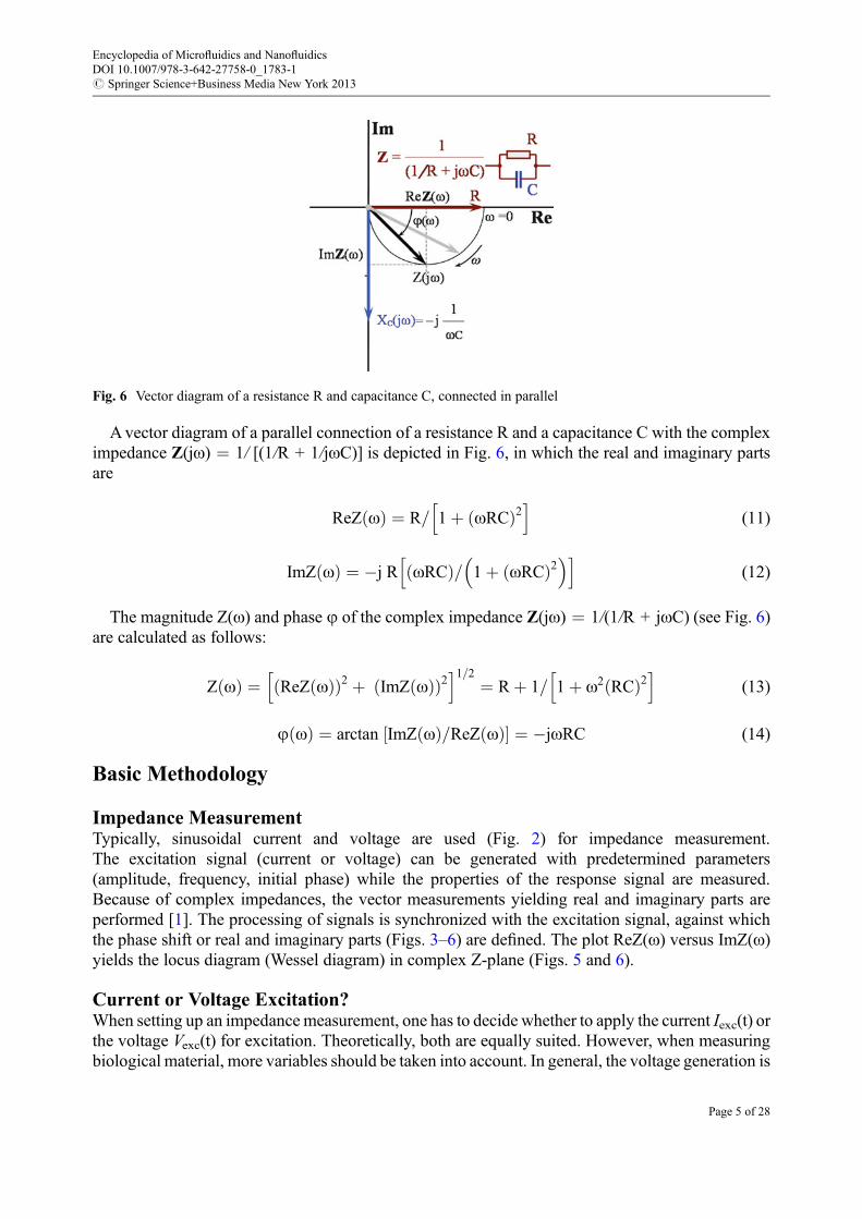
Avector diagram of a parallel connection of a resistance R and a capacitance C with the compleximpedance Z(jo) ¼ 1/ [(1/R + 1/joC)] is depicted in Fig. 6, in which the real and imaginary partsare
ReZ oð Þ ¼ R= 1þ oRCð Þ2h i
(11)
ImZ oð Þ ¼ �j R oRCð Þ= 1þ oRCð Þ2� �h i
(12)
The magnitude Z(o) and phase j of the complex impedance Z(jo) ¼ 1/(1/R + joC) (see Fig. 6)are calculated as follows:
Z oð Þ ¼ ReZ oð Þð Þ2 þ ImZ oð Þð Þ2h i1=2
¼ Rþ 1= 1þ o2 RCð Þ2h i
(13)
j oð Þ ¼ arctan ImZ oð Þ=ReZ oð Þ½ � ¼ �joRC (14)
Basic Methodology
Impedance MeasurementTypically, sinusoidal current and voltage are used (Fig. 2) for impedance measurement.The excitation signal (current or voltage) can be generated with predetermined parameters(amplitude, frequency, initial phase) while the properties of the response signal are measured.Because of complex impedances, the vector measurements yielding real and imaginary parts areperformed [1]. The processing of signals is synchronized with the excitation signal, against whichthe phase shift or real and imaginary parts (Figs. 3–6) are defined. The plot ReZ(o) versus ImZ(o)yields the locus diagram (Wessel diagram) in complex Z-plane (Figs. 5 and 6).
Current or Voltage Excitation?When setting up an impedance measurement, one has to decide whether to apply the current Iexc(t) orthe voltage Vexc(t) for excitation. Theoretically, both are equally suited. However, when measuringbiological material, more variables should be taken into account. In general, the voltage generation is
Fig. 6 Vector diagram of a resistance R and capacitance C, connected in parallel
Encyclopedia of Microfluidics and NanofluidicsDOI 10.1007/978-3-642-27758-0_1783-1# Springer Science+Business Media New York 2013
Page 5 of 28
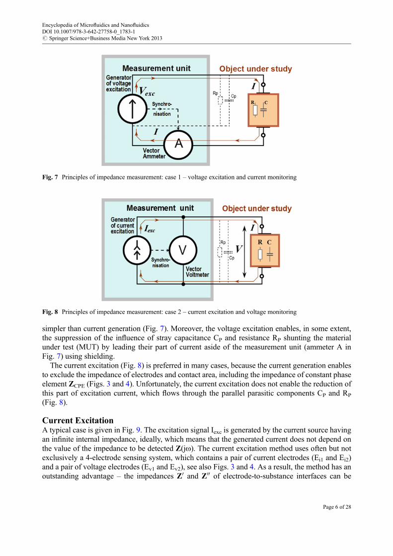
simpler than current generation (Fig. 7). Moreover, the voltage excitation enables, in some extent,the suppression of the influence of stray capacitance CP and resistance RP shunting the materialunder test (MUT) by leading their part of current aside of the measurement unit (ammeter A inFig. 7) using shielding.
The current excitation (Fig. 8) is preferred in many cases, because the current generation enablesto exclude the impedance of electrodes and contact area, including the impedance of constant phaseelement ZCPE (Figs. 3 and 4). Unfortunately, the current excitation does not enable the reduction ofthis part of excitation current, which flows through the parallel parasitic components CP and RP
(Fig. 8).
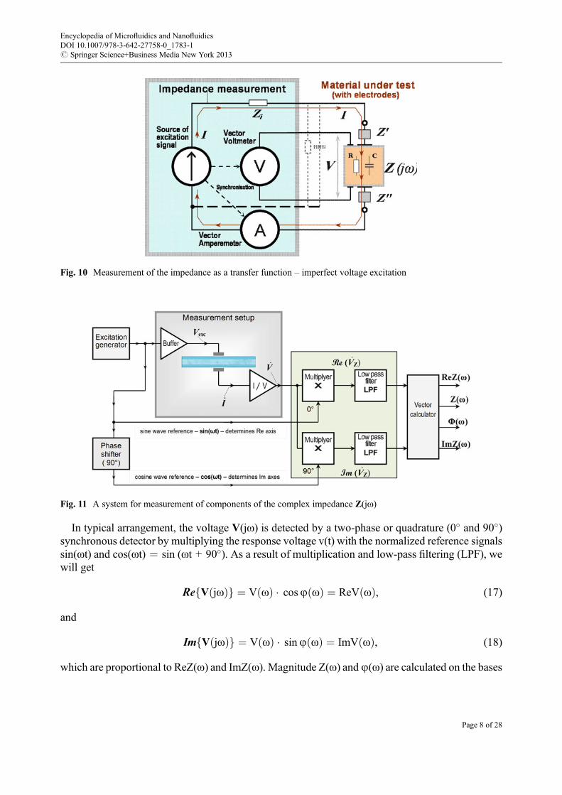
Current ExcitationA typical case is given in Fig. 9. The excitation signal Iexc is generated by the current source havingan infinite internal impedance, ideally, which means that the generated current does not depend onthe value of the impedance to be detected Z(jo). The current excitation method uses often but notexclusively a 4-electrode sensing system, which contains a pair of current electrodes (Ei1 and Ei2)and a pair of voltage electrodes (Ev1 and Ev2), see also Figs. 3 and 4. As a result, the method has anoutstanding advantage – the impedances Z0 and Z00 of electrode-to-substance interfaces can be
Fig. 7 Principles of impedance measurement: case 1 – voltage excitation and current monitoring
Fig. 8 Principles of impedance measurement: case 2 – current excitation and voltage monitoring
Encyclopedia of Microfluidics and NanofluidicsDOI 10.1007/978-3-642-27758-0_1783-1# Springer Science+Business Media New York 2013
Page 6 of 28
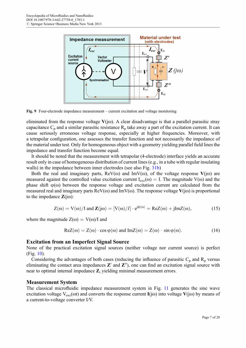
eliminated from the response voltage V(jo). A clear disadvantage is that a parallel parasitic straycapacitance Cp and a similar parasitic resistance Rp take away a part of the excitation current. It cancause seriously erroneous voltage response, especially at higher frequencies. Moreover, witha tetrapolar configuration, one assesses the transfer function and not necessarily the impedance ofthe material under test. Only for homogeneous object with a geometry yielding parallel field lines theimpedance and transfer function become equal.
It should be noted that the measurement with tetrapolar (4-electrode) interface yields an accurateresult only in case of homogeneous distribution of current lines (e.g., in a tube with regular insulatingwalls) in the impedance between inner electrodes (see also Fig. 31b)
Both the real and imaginary parts, ReV(o) and ImV(o), of the voltage response V(jo) aremeasured against the controlled value excitation current Iexc(o) ¼ I. The magnitude V(o) and thephase shift j(o) between the response voltage and excitation current are calculated from themeasured real and imaginary parts ReV(o) and ImV(o). The response voltage V(jo) is proportionalto the impedance Z(jo):
Z oð Þ ¼ V oð Þ=I and Z joð Þ ¼ V oð Þ=I½ � � ejf oð Þ ¼ ReZ oð Þ þ jImZ oð Þ, (15)
where the magnitude Z(o) ¼ V(o)/I and
ReZ oð Þ ¼ Z oð Þ � cosj oð Þ and ImZ oð Þ ¼ Z oð Þ � sinj oð Þ: (16)
Excitation from an Imperfect Signal SourceNone of the practical excitation signal sources (neither voltage nor current source) is perfect(Fig. 10).
Considering the advantages of both cases (reducing the influence of parasitic Cp and Rp versuseliminating the contact area impedances Z0 and Z00), one can find an excitation signal source withnear to optimal internal impedance Zi yielding minimal measurement errors.
Measurement SystemThe classical microfluidic impedance measurement system in Fig. 11 generates the sine waveexcitation voltage Vexc(ot) and converts the response current I(jo) into voltage V(jo) by means ofa current-to-voltage converter I/V.
Fig. 9 Four-electrode impedance measurement – current excitation and voltage monitoring
Encyclopedia of Microfluidics and NanofluidicsDOI 10.1007/978-3-642-27758-0_1783-1# Springer Science+Business Media New York 2013
Page 7 of 28
In typical arrangement, the voltage V(jo) is detected by a two-phase or quadrature (0� and 90�)synchronous detector by multiplying the response voltage v(t) with the normalized reference signalssin(ot) and cos(ot) ¼ sin (ot + 90�). As a result of multiplication and low-pass filtering (LPF), wewill get
Re V joð Þf g ¼ V oð Þ � cosj oð Þ ¼ ReV oð Þ, (17)
and
Im V joð Þf g ¼ V oð Þ � sinj oð Þ ¼ ImV oð Þ, (18)
which are proportional to ReZ(o) and ImZ(o). Magnitude Z(o) andj(o) are calculated on the bases
Fig. 11 A system for measurement of components of the complex impedance Z(jo)
Fig. 10 Measurement of the impedance as a transfer function – imperfect voltage excitation
Encyclopedia of Microfluidics and NanofluidicsDOI 10.1007/978-3-642-27758-0_1783-1# Springer Science+Business Media New York 2013
Page 8 of 28
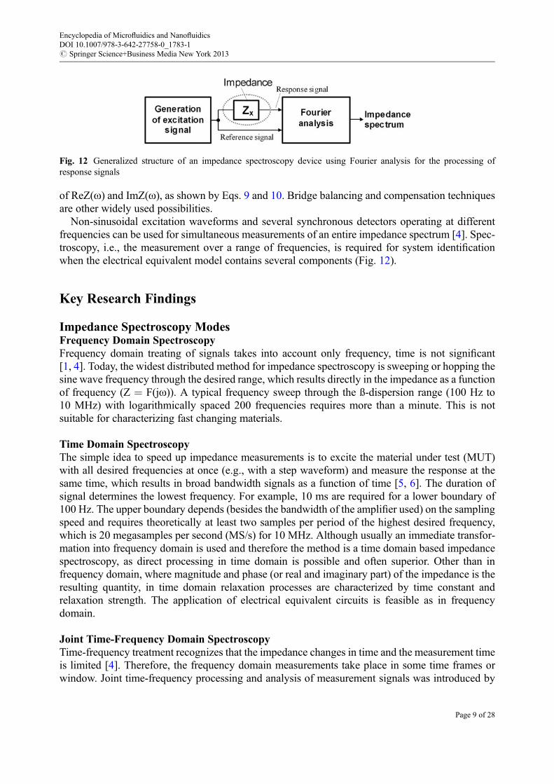
of ReZ(o) and ImZ(o), as shown by Eqs. 9 and 10. Bridge balancing and compensation techniquesare other widely used possibilities.
Non-sinusoidal excitation waveforms and several synchronous detectors operating at differentfrequencies can be used for simultaneous measurements of an entire impedance spectrum [4]. Spec-troscopy, i.e., the measurement over a range of frequencies, is required for system identificationwhen the electrical equivalent model contains several components (Fig. 12).
Key Research Findings
Impedance Spectroscopy ModesFrequency Domain SpectroscopyFrequency domain treating of signals takes into account only frequency, time is not significant[1, 4]. Today, the widest distributed method for impedance spectroscopy is sweeping or hopping thesine wave frequency through the desired range, which results directly in the impedance as a functionof frequency (Z ¼ F(jo)). A typical frequency sweep through the ß-dispersion range (100 Hz to10 MHz) with logarithmically spaced 200 frequencies requires more than a minute. This is notsuitable for characterizing fast changing materials.
Time Domain SpectroscopyThe simple idea to speed up impedance measurements is to excite the material under test (MUT)with all desired frequencies at once (e.g., with a step waveform) and measure the response at thesame time, which results in broad bandwidth signals as a function of time [5, 6]. The duration ofsignal determines the lowest frequency. For example, 10 ms are required for a lower boundary of100 Hz. The upper boundary depends (besides the bandwidth of the amplifier used) on the samplingspeed and requires theoretically at least two samples per period of the highest desired frequency,which is 20 megasamples per second (MS/s) for 10 MHz. Although usually an immediate transfor-mation into frequency domain is used and therefore the method is a time domain based impedancespectroscopy, as direct processing in time domain is possible and often superior. Other than infrequency domain, where magnitude and phase (or real and imaginary part) of the impedance is theresulting quantity, in time domain relaxation processes are characterized by time constant andrelaxation strength. The application of electrical equivalent circuits is feasible as in frequencydomain.
Joint Time-Frequency Domain SpectroscopyTime-frequency treatment recognizes that the impedance changes in time and the measurement timeis limited [4]. Therefore, the frequency domain measurements take place in some time frames orwindow. Joint time-frequency processing and analysis of measurement signals was introduced by
Fig. 12 Generalized structure of an impedance spectroscopy device using Fourier analysis for the processing ofresponse signals
Encyclopedia of Microfluidics and NanofluidicsDOI 10.1007/978-3-642-27758-0_1783-1# Springer Science+Business Media New York 2013
Page 9 of 28
Dennis Gabor in the 1940s. Nowadays, different versions of short-time and fractionalFourier transform have been developed, yielding a time-varying frequency spectrum of theimpedance.
Impedance Spectroscopy with Spectrally Rich SignalsUsing broad bandwidth signals for excitation rather than sinusoids together with simultaneousdetection reduces greatly the measurement time. Although simultaneous detection is possible byhardware, in most cases signals are traced as function of time (time domain) and afterwardstransformed into frequency domain.
Multisine ExcitationThe idea is to use a sum of sine waves with different predetermined frequencies for excitation.A multisine excitation signal Sexc(t) with frequencies f1 to fk of k sine wave components can beexpressed as
Sexc tð Þ ¼Xi¼k
i¼l
Ai � sin 2pf i þ Fið Þ (19)
where Ai is the amplitude of the i-th component and Fi is its initial phase. An optimal synthesis isrequired for determination of the most favorable initial phasesFi. The problem is in minimization ofthe peak value of the multisine signal against its root-mean-square (RMS) value, that is, the minimalcrest factor CF ¼ (peak value)/(RMS value) is required.
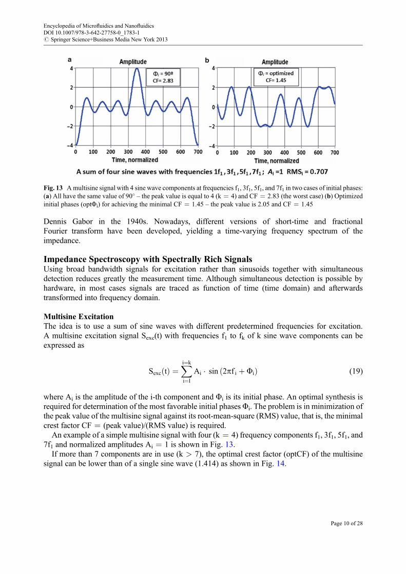
An example of a simple multisine signal with four (k ¼ 4) frequency components f1, 3f1, 5f1, and7f1 and normalized amplitudes Ai ¼ 1 is shown in Fig. 13.
If more than 7 components are in use (k > 7), the optimal crest factor (optCF) of the multisinesignal can be lower than of a single sine wave (1.414) as shown in Fig. 14.
Fig. 13 Amultisine signal with 4 sine wave components at frequencies f1, 3f1, 5f1, and 7f1 in two cases of initial phases:(a) All have the same value of 90� – the peak value is equal to 4 (k ¼ 4) and CF ¼ 2.83 (the worst case) (b) Optimizedinitial phases (optFi) for achieving the minimal CF ¼ 1.45 – the peak value is 2.05 and CF ¼ 1.45
Encyclopedia of Microfluidics and NanofluidicsDOI 10.1007/978-3-642-27758-0_1783-1# Springer Science+Business Media New York 2013
Page 10 of 28
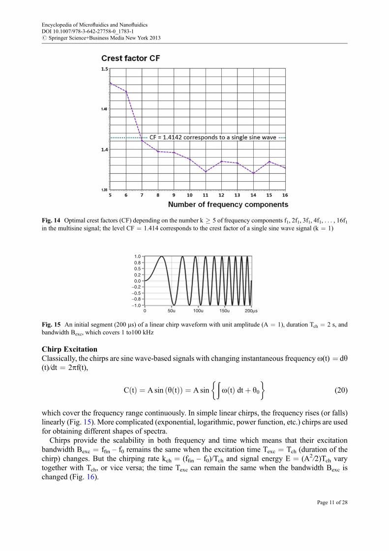
Chirp ExcitationClassically, the chirps are sine wave-based signals with changing instantaneous frequencyo(t) ¼ dy(t)/dt ¼ 2pf(t),
C tð Þ ¼ A sin ðy tÞð Þ ¼ A sin
ðo tð Þ dtþ y0
� �(20)
which cover the frequency range continuously. In simple linear chirps, the frequency rises (or falls)linearly (Fig. 15). More complicated (exponential, logarithmic, power function, etc.) chirps are usedfor obtaining different shapes of spectra.
Chirps provide the scalability in both frequency and time which means that their excitationbandwidth Bexc ¼ ffin – f0 remains the same when the excitation time Texc ¼ Tch (duration of thechirp) changes. But the chirping rate kch ¼ (ffin – f0)/Tch and signal energy E ¼ (A2/2)Tch varytogether with Tch, or vice versa; the time Texc can remain the same when the bandwidth Bexc ischanged (Fig. 16).
Fig. 14 Optimal crest factors (CF) depending on the number k � 5 of frequency components f1, 2f1, 3f1, 4f1, . . . , 16f1in the multisine signal; the level CF ¼ 1.414 corresponds to the crest factor of a single sine wave signal (k ¼ 1)
1.00.80.50.20.0
−0.2−0.5−0.8−1.0
0 50u 100u 200μs150u
Fig. 15 An initial segment (200 ms) of a linear chirp waveform with unit amplitude (A ¼ 1), duration Tch ¼ 2 s, andbandwidth Bexc, which covers 1 to100 kHz
Encyclopedia of Microfluidics and NanofluidicsDOI 10.1007/978-3-642-27758-0_1783-1# Springer Science+Business Media New York 2013
Page 11 of 28

In using nonlinear chirps with the frequency increasing by a power function, the chirping rateexpresses as follows:
kch ¼ f fin � f oð Þ=Tnch (21)
The chirp function Eq. 20 obtains the following form (n is the order of power function) in thiscase:
Cn tð Þ ¼ A sin 2p f 0 � tþ kch � tnþ1= nþ 1ð Þð Þð Þ (22)
What is important is that over 90 % of generated excitation energy falls into the desired excitationbandwidth Bexc. There are two possibilities to convert the time domain chirp responses intofrequency domain spectra (Fig. 17a, b) using fast Fourier transform (FFT).
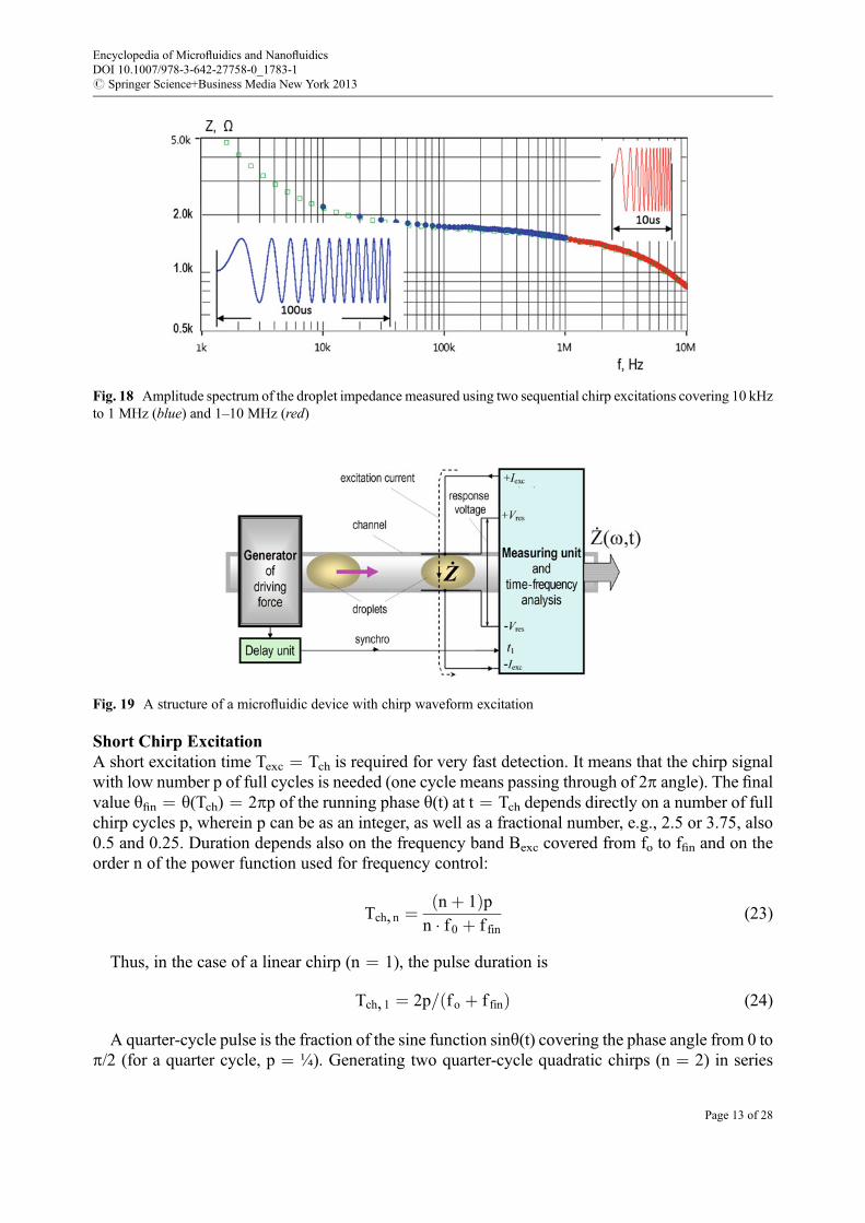
A droplet detection microfluidic system with chirp excitation (Fig. 18) is shown in Fig. 19 [4].
Fig. 16 Normalized RMS (root-mean-square) spectral density distribution of the chirp signal presented in Fig. 15;99.97 % of the generated energy is concentrated into the desired bandwidth Bexc
Fig. 17 Two methods for impedance spectroscopy using fast Fourier transform (FFT): (a) Through transforming ofcross-correlation function (b) Through dividing of transformed response and excitation signals
Encyclopedia of Microfluidics and NanofluidicsDOI 10.1007/978-3-642-27758-0_1783-1# Springer Science+Business Media New York 2013
Page 12 of 28
Short Chirp ExcitationA short excitation time Texc ¼ Tch is required for very fast detection. It means that the chirp signalwith low number p of full cycles is needed (one cycle means passing through of 2p angle). The finalvalue yfin ¼ y(Tch) ¼ 2pp of the running phase y(t) at t ¼ Tch depends directly on a number of fullchirp cycles p, wherein p can be as an integer, as well as a fractional number, e.g., 2.5 or 3.75, also0.5 and 0.25. Duration depends also on the frequency band Bexc covered from fo to ffin and on theorder n of the power function used for frequency control:
Tch, n ¼ nþ 1ð Þpn � f 0 þ f fin
(23)
Thus, in the case of a linear chirp (n ¼ 1), the pulse duration is
Tch, 1 ¼ 2p= f o þ f finð Þ (24)
A quarter-cycle pulse is the fraction of the sine function siny(t) covering the phase angle from 0 top/2 (for a quarter cycle, p ¼ ¼). Generating two quarter-cycle quadratic chirps (n ¼ 2) in series
Fig. 18 Amplitude spectrum of the droplet impedance measured using two sequential chirp excitations covering 10 kHzto 1 MHz (blue) and 1–10 MHz (red)
Fig. 19 A structure of a microfluidic device with chirp waveform excitation
Encyclopedia of Microfluidics and NanofluidicsDOI 10.1007/978-3-642-27758-0_1783-1# Springer Science+Business Media New York 2013
Page 13 of 28
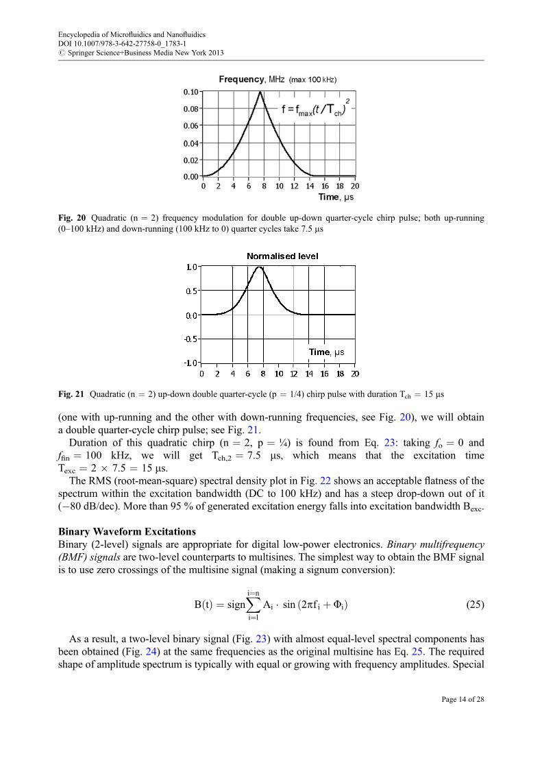
(one with up-running and the other with down-running frequencies, see Fig. 20), we will obtaina double quarter-cycle chirp pulse; see Fig. 21.
Duration of this quadratic chirp (n ¼ 2, p ¼ ¼) is found from Eq. 23: taking fo ¼ 0 andffin ¼ 100 kHz, we will get Tch,2 ¼ 7.5 ms, which means that the excitation timeTexc ¼ 2 � 7.5 ¼ 15 ms.
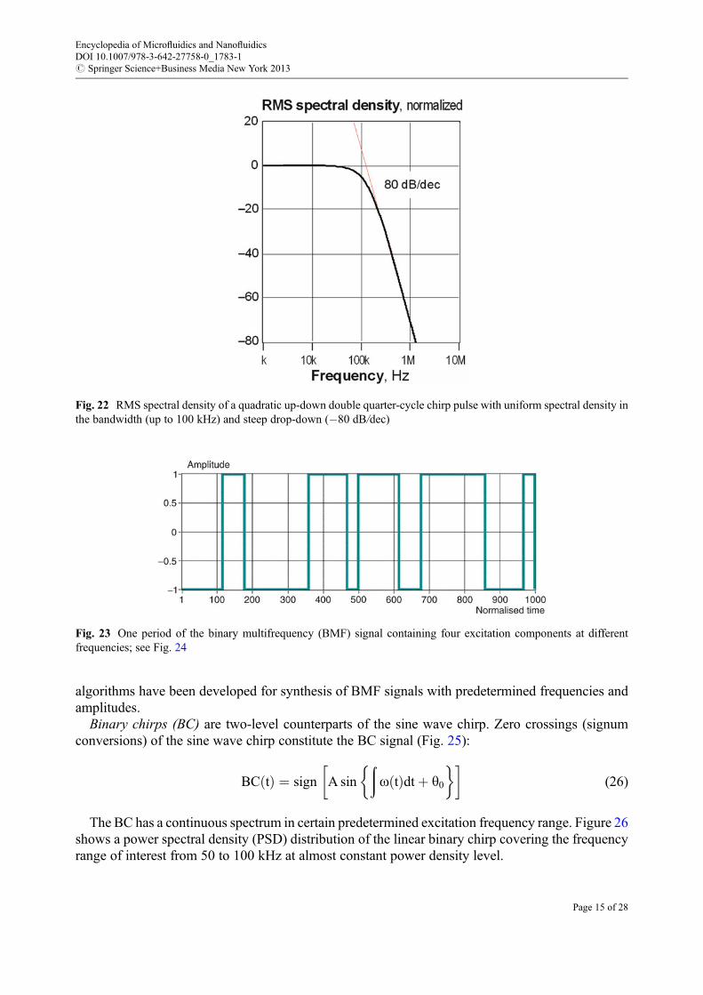
The RMS (root-mean-square) spectral density plot in Fig. 22 shows an acceptable flatness of thespectrum within the excitation bandwidth (DC to 100 kHz) and has a steep drop-down out of it(�80 dB/dec). More than 95 % of generated excitation energy falls into excitation bandwidth Bexc.
Binary Waveform ExcitationsBinary (2-level) signals are appropriate for digital low-power electronics. Binary multifrequency(BMF) signals are two-level counterparts to multisines. The simplest way to obtain the BMF signalis to use zero crossings of the multisine signal (making a signum conversion):
B tð Þ ¼ signXi¼n
i¼l
Ai � sin 2pf i þ Fið Þ (25)
As a result, a two-level binary signal (Fig. 23) with almost equal-level spectral components hasbeen obtained (Fig. 24) at the same frequencies as the original multisine has Eq. 25. The requiredshape of amplitude spectrum is typically with equal or growing with frequency amplitudes. Special
Fig. 20 Quadratic (n ¼ 2) frequency modulation for double up-down quarter-cycle chirp pulse; both up-running(0–100 kHz) and down-running (100 kHz to 0) quarter cycles take 7.5 ms
Fig. 21 Quadratic (n ¼ 2) up-down double quarter-cycle (p ¼ 1/4) chirp pulse with duration Tch ¼ 15 ms
Encyclopedia of Microfluidics and NanofluidicsDOI 10.1007/978-3-642-27758-0_1783-1# Springer Science+Business Media New York 2013
Page 14 of 28
algorithms have been developed for synthesis of BMF signals with predetermined frequencies andamplitudes.
Binary chirps (BC) are two-level counterparts of the sine wave chirp. Zero crossings (signumconversions) of the sine wave chirp constitute the BC signal (Fig. 25):
BC tð Þ ¼ sign A sin
ðo tð Þdtþ y0
� �� �(26)
The BC has a continuous spectrum in certain predetermined excitation frequency range. Figure 26shows a power spectral density (PSD) distribution of the linear binary chirp covering the frequencyrange of interest from 50 to 100 kHz at almost constant power density level.
Fig. 22 RMS spectral density of a quadratic up-down double quarter-cycle chirp pulse with uniform spectral density inthe bandwidth (up to 100 kHz) and steep drop-down (�80 dB/dec)
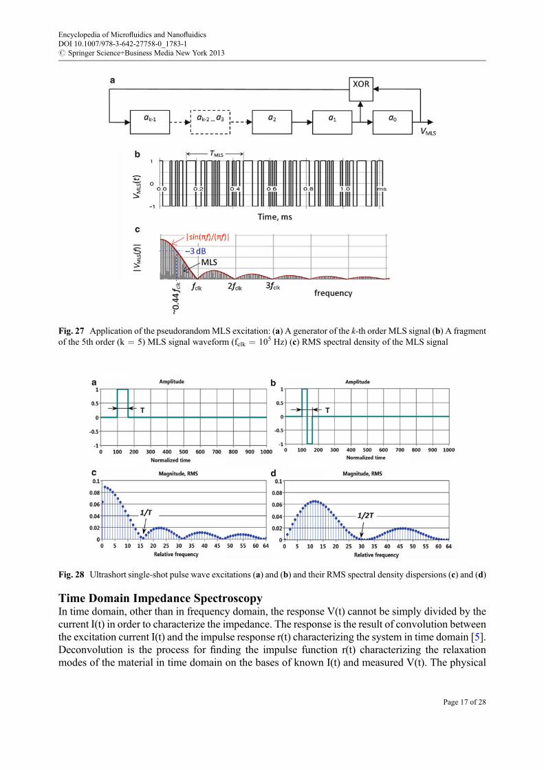
Fig. 23 One period of the binary multifrequency (BMF) signal containing four excitation components at differentfrequencies; see Fig. 24
Encyclopedia of Microfluidics and NanofluidicsDOI 10.1007/978-3-642-27758-0_1783-1# Springer Science+Business Media New York 2013
Page 15 of 28

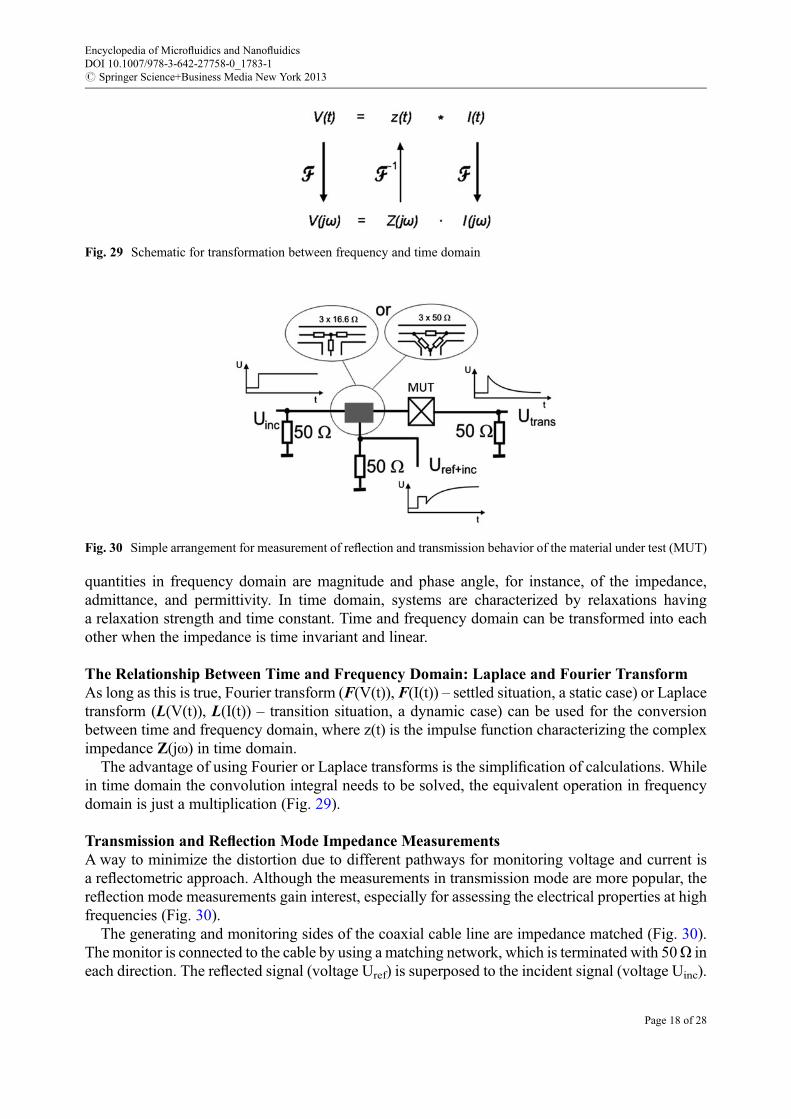
A binary pseudorandom excitation is the simplest to generate signal [7]. It can be formed directlyfrom a clock signal with frequency fclk using the sequence of k trigger circuits (a0 to ak�1)constituting a shift register (Fig. 27a). The shift register is feedbacked through an exclusive OR(XOR) logic element. The number of produced random pulses is N ¼ 2k�1. This pattern is a periodof the maximum length sequence (MLS) with duration TMLS ¼ N/fclk (Fig. 27b). The MLS hasa continuous RMS spectral density expressed via the sinus cardinalis function (|sin(pf)/(pf)|); seeFig. 27c. It has enough power up to the frequency, at which the power spectral density PSD stillretains its 50 % level (�3 dB RMS level).
Binary ultrashort excitations are the rectangular single-pulse (one-shot) excitations (Fig. 28),which are in use when a very short time domain spectroscopy is required. A serious disadvantage ofthe ultrashort pulse excitations is their low spectral density within the excitation bandwidth, whichshould be compensated by logarithmically spaced sampling intervals, when digitizing the responsesignal.
Magnitude, RMS1
00 1 2 3 4 5 6 8 10
Relative frequency97
0.8
0.6
0.4
0.2
Fig. 24 Amplitude spectrum of the BMF signal given in Fig. 23, which contains four spectral components at differentfrequencies (1f, 3f, 5f, 7f)
Fig. 25 Waveform of a linear binary chirp (BC)
Fig. 26 Power spectral density (PSD) distribution of a binary linear chirp in the excitation bandwidth Bexc from 50 to100 kHz (Z ¼ R ¼ 1 kO)
Encyclopedia of Microfluidics and NanofluidicsDOI 10.1007/978-3-642-27758-0_1783-1# Springer Science+Business Media New York 2013
Page 16 of 28
Time Domain Impedance SpectroscopyIn time domain, other than in frequency domain, the response V(t) cannot be simply divided by thecurrent I(t) in order to characterize the impedance. The response is the result of convolution betweenthe excitation current I(t) and the impulse response r(t) characterizing the system in time domain [5].Deconvolution is the process for finding the impulse function r(t) characterizing the relaxationmodes of the material in time domain on the bases of known I(t) and measured V(t). The physical
Fig. 27 Application of the pseudorandomMLS excitation: (a) A generator of the k-th order MLS signal (b) A fragmentof the 5th order (k ¼ 5) MLS signal waveform (fclk ¼ 105 Hz) (c) RMS spectral density of the MLS signal
Fig. 28 Ultrashort single-shot pulse wave excitations (a) and (b) and their RMS spectral density dispersions (c) and (d)
Encyclopedia of Microfluidics and NanofluidicsDOI 10.1007/978-3-642-27758-0_1783-1# Springer Science+Business Media New York 2013
Page 17 of 28
quantities in frequency domain are magnitude and phase angle, for instance, of the impedance,admittance, and permittivity. In time domain, systems are characterized by relaxations havinga relaxation strength and time constant. Time and frequency domain can be transformed into eachother when the impedance is time invariant and linear.
The Relationship Between Time and Frequency Domain: Laplace and Fourier TransformAs long as this is true, Fourier transform (F(V(t)), F(I(t)) – settled situation, a static case) or Laplacetransform (L(V(t)), L(I(t)) – transition situation, a dynamic case) can be used for the conversionbetween time and frequency domain, where z(t) is the impulse function characterizing the compleximpedance Z(jo) in time domain.
The advantage of using Fourier or Laplace transforms is the simplification of calculations. Whilein time domain the convolution integral needs to be solved, the equivalent operation in frequencydomain is just a multiplication (Fig. 29).
Transmission and Reflection Mode Impedance MeasurementsA way to minimize the distortion due to different pathways for monitoring voltage and current isa reflectometric approach. Although the measurements in transmission mode are more popular, thereflection mode measurements gain interest, especially for assessing the electrical properties at highfrequencies (Fig. 30).
The generating and monitoring sides of the coaxial cable line are impedance matched (Fig. 30).The monitor is connected to the cable by using a matching network, which is terminated with 50O ineach direction. The reflected signal (voltage Uref) is superposed to the incident signal (voltage Uinc).
Fig. 29 Schematic for transformation between frequency and time domain
Fig. 30 Simple arrangement for measurement of reflection and transmission behavior of the material under test (MUT)
Encyclopedia of Microfluidics and NanofluidicsDOI 10.1007/978-3-642-27758-0_1783-1# Springer Science+Business Media New York 2013
Page 18 of 28
Because of the superposition, both the incident and the reflected signals are amplified with the samehardware, which reduces the influence of poorly matched input amplifiers and ADC.
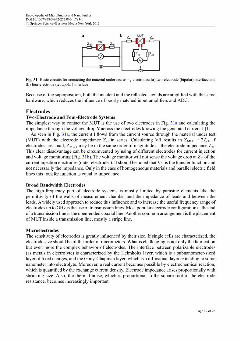
ElectrodesTwo-Electrode and Four-Electrode SystemsThe simplest way to contact the MUT is the use of two electrodes in Fig. 31a and calculating theimpedance through the voltage drop V across the electrodes knowing the generated current I [1].
As seen in Fig. 31a, the current I flows from the current source through the material under test(MUT) with the electrode impedance Zel in series. Calculating V/I results in ZMUT + 2Zel. Ifelectrodes are small, ZMUT may be in the same order of magnitude as the electrode impedance Zel.This clear disadvantage can be circumvented by using of different electrodes for current injectionand voltage monitoring (Fig. 31b). The voltage monitor will not sense the voltage drop at Zel of thecurrent injection electrodes (outer electrodes). It should be noted that V/I is the transfer function andnot necessarily the impedance. Only in the case of homogeneous materials and parallel electric fieldlines this transfer function is equal to impedance.
Broad Bandwidth ElectrodesThe high-frequency part of electrode systems is mostly limited by parasitic elements like thepermittivity of the walls of measurement chamber and the impedance of leads and between theleads. Awidely used approach to reduce this influence and to increase the useful frequency range ofelectrodes up to GHz is the use of transmission lines. Most popular electrode configuration at the endof a transmission line is the open-ended coaxial line. Another common arrangement is the placementof MUT inside a transmission line, mostly a stripe line.
MicroelectrodesThe sensitivity of electrodes is greatly influenced by their size. If single cells are characterized, theelectrode size should be of the order of micrometers. What is challenging is not only the fabricationbut even more the complex behavior of electrodes. The interface between polarizable electrodes(as metals in electrolyte) is characterized by the Helmholtz layer, which is a subnanometer-sizedlayer of fixed charges, and the Gouy-Chapman layer, which is a diffusional layer extending to somenanometer into electrolyte. Moreover, a real current becomes possible by electrochemical reaction,which is quantified by the exchange current density. Electrode impedance arises proportionally withshrinking size. Also, the thermal noise, which is proportional to the square root of the electroderesistance, becomes increasingly important.
Zel
a b
ZelMUT
Zel Zel
Zel Zel
MUT
V
IV
I
Fig. 31 Basic circuits for contacting the material under test using electrodes: (a) two-electrode (bipolar) interface and(b) four-electrode (tetrapolar) interface
Encyclopedia of Microfluidics and NanofluidicsDOI 10.1007/978-3-642-27758-0_1783-1# Springer Science+Business Media New York 2013
Page 19 of 28
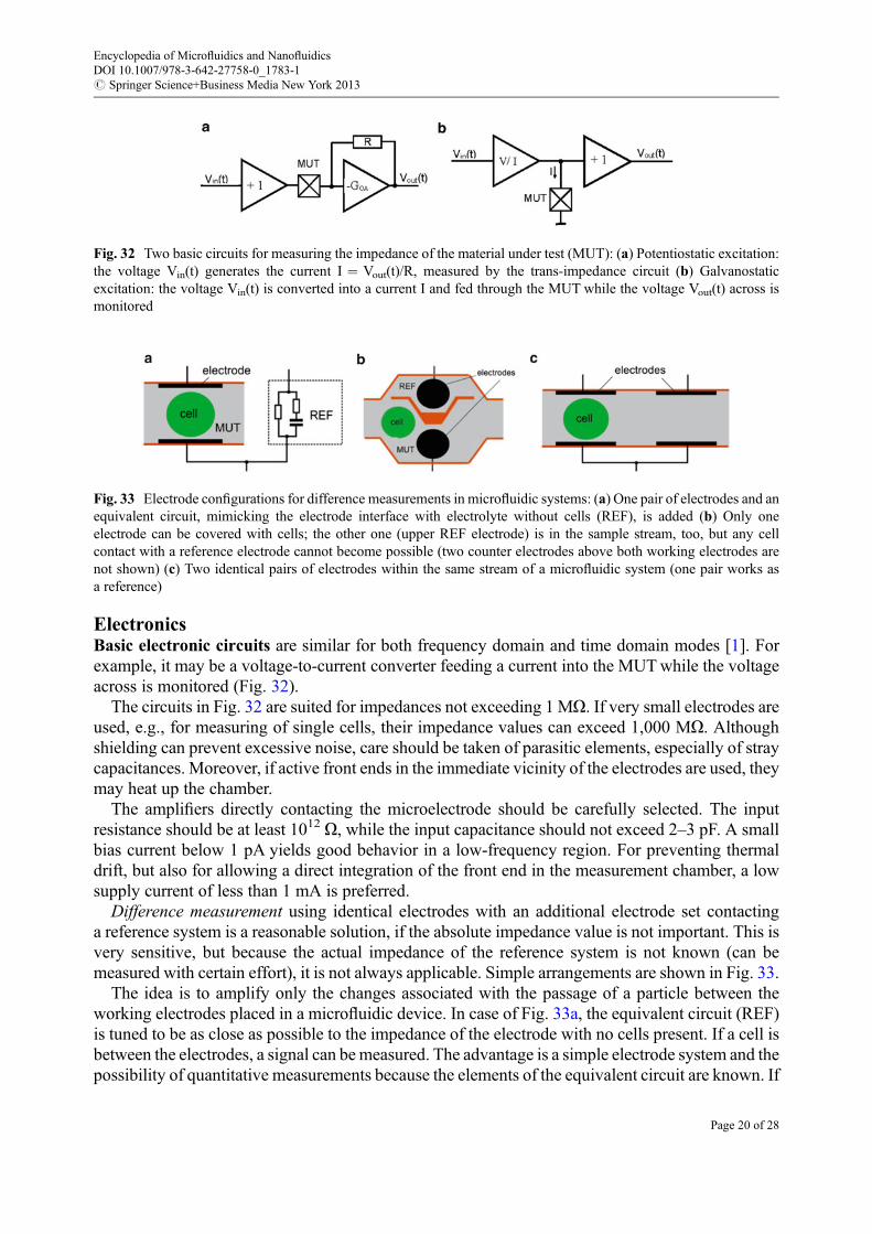
ElectronicsBasic electronic circuits are similar for both frequency domain and time domain modes [1]. Forexample, it may be a voltage-to-current converter feeding a current into the MUTwhile the voltageacross is monitored (Fig. 32).
The circuits in Fig. 32 are suited for impedances not exceeding 1 MO. If very small electrodes areused, e.g., for measuring of single cells, their impedance values can exceed 1,000 MO. Althoughshielding can prevent excessive noise, care should be taken of parasitic elements, especially of straycapacitances. Moreover, if active front ends in the immediate vicinity of the electrodes are used, theymay heat up the chamber.
The amplifiers directly contacting the microelectrode should be carefully selected. The inputresistance should be at least 1012 O, while the input capacitance should not exceed 2–3 pF. A smallbias current below 1 pA yields good behavior in a low-frequency region. For preventing thermaldrift, but also for allowing a direct integration of the front end in the measurement chamber, a lowsupply current of less than 1 mA is preferred.
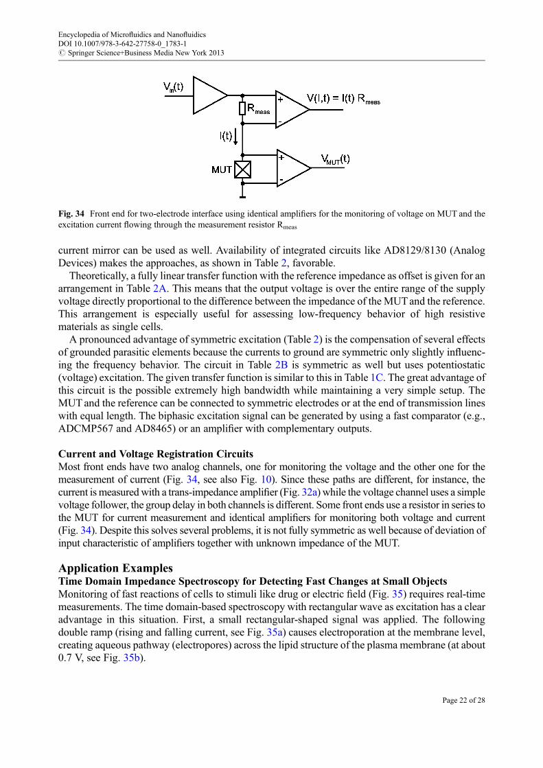
Difference measurement using identical electrodes with an additional electrode set contactinga reference system is a reasonable solution, if the absolute impedance value is not important. This isvery sensitive, but because the actual impedance of the reference system is not known (can bemeasured with certain effort), it is not always applicable. Simple arrangements are shown in Fig. 33.
The idea is to amplify only the changes associated with the passage of a particle between theworking electrodes placed in a microfluidic device. In case of Fig. 33a, the equivalent circuit (REF)is tuned to be as close as possible to the impedance of the electrode with no cells present. If a cell isbetween the electrodes, a signal can bemeasured. The advantage is a simple electrode system and thepossibility of quantitative measurements because the elements of the equivalent circuit are known. If
Fig. 32 Two basic circuits for measuring the impedance of the material under test (MUT): (a) Potentiostatic excitation:the voltage Vin(t) generates the current I ¼ Vout(t)/R, measured by the trans-impedance circuit (b) Galvanostaticexcitation: the voltage Vin(t) is converted into a current I and fed through the MUT while the voltage Vout(t) across ismonitored
Fig. 33 Electrode configurations for difference measurements in microfluidic systems: (a) One pair of electrodes and anequivalent circuit, mimicking the electrode interface with electrolyte without cells (REF), is added (b) Only oneelectrode can be covered with cells; the other one (upper REF electrode) is in the sample stream, too, but any cellcontact with a reference electrode cannot become possible (two counter electrodes above both working electrodes arenot shown) (c) Two identical pairs of electrodes within the same stream of a microfluidic system (one pair works asa reference)
Encyclopedia of Microfluidics and NanofluidicsDOI 10.1007/978-3-642-27758-0_1783-1# Springer Science+Business Media New York 2013
Page 20 of 28

quantitative assessment of the MUT behavior is not important, an arrangement in Fig. 33b has theadvantage, because the reference electrode (REF) has theoretically the same impedance as theworking electrode. This enhances the sensitivity tremendously.
If two pairs of electrodes in a microfluidic system are arranged in series, as shown in Fig. 33c, andthe voltage difference due to equal current at both electrode pairs is monitored (similar to Table 2A),it triggers two events subsequently with opposite polarity. This arrangement is very robust, becausethe false detection will be canceled due to the missing signal of opposite polarity.
Differential Front EndsThe signal generated by a cell passing the electrode system depends not only on electrode and cellgeometry but also on the medium conductivity and the analog front end used. Although it is simpleto calculate the impedance Z of the MUT between electrodes, the robustness depends on severalfactors. Ideally, the transfer function between Z and Vout is linear and the offset is as small aspossible. But looking at the transfer functions in Table 1, none of the circuits show linear dependenceof the measured difference voltage on the impedance value. Nonlinear relationship between Z andVout is common to all the three cases A, B, and C.
Careful design of the front end (Table 2) can considerably increase the performance. Theadvantage is most pronounced for miniaturized electrodes with low sensitivity. Since the electrodeimpedance depends considerably on current density, it is advisable to hold the current densityconstant or the same in the MUT and reference branch, as it is accomplished in Table 2A (currentexcitation). A symmetric Howland-type current source supplies both the MUT and the referencewith a current of the same amplitude but opposite polarity. Although, a single current source with
Table 2 Front ends with symmetric excitation: A galvanostatic, B potentiostatic
A B
Uin(t) Rmeas
refRmeas
R
R
R
RUout(t)
MUT
+1
+
−
+
−
Uin(t)
ref
+1Uout(t)
MUT
ZX ¼ RmeasV in
V out þ Zr ZX ¼ ZrV in�V outV inþV out
Table 1 Common front-end configurations for measurement of difference between the impedance of material under test(MUT) and impedance of a reference (ref)
A B C
Uin(t)
ref
R R
Uout(t)
MUT+
−
Uin(t)
ref
R
R
Uout(t)
MUT
−1
−1
+
−
Uin(t)
ref R
R
Uout(t)
MUT
+
−
ZX¼R V in�V outð Þ ZrþRð Þ�V inRV out ZrþRð ÞþV inR
h iZX ¼ V in R�Zrð Þ
V inRþV outZrZX ¼ Zr
V in�2V outV inþ2V out
Encyclopedia of Microfluidics and NanofluidicsDOI 10.1007/978-3-642-27758-0_1783-1# Springer Science+Business Media New York 2013
Page 21 of 28
current mirror can be used as well. Availability of integrated circuits like AD8129/8130 (AnalogDevices) makes the approaches, as shown in Table 2, favorable.
Theoretically, a fully linear transfer function with the reference impedance as offset is given for anarrangement in Table 2A. This means that the output voltage is over the entire range of the supplyvoltage directly proportional to the difference between the impedance of the MUTand the reference.This arrangement is especially useful for assessing low-frequency behavior of high resistivematerials as single cells.
A pronounced advantage of symmetric excitation (Table 2) is the compensation of several effectsof grounded parasitic elements because the currents to ground are symmetric only slightly influenc-ing the frequency behavior. The circuit in Table 2B is symmetric as well but uses potentiostatic(voltage) excitation. The given transfer function is similar to this in Table 1C. The great advantage ofthis circuit is the possible extremely high bandwidth while maintaining a very simple setup. TheMUTand the reference can be connected to symmetric electrodes or at the end of transmission lineswith equal length. The biphasic excitation signal can be generated by using a fast comparator (e.g.,ADCMP567 and AD8465) or an amplifier with complementary outputs.
Current and Voltage Registration CircuitsMost front ends have two analog channels, one for monitoring the voltage and the other one for themeasurement of current (Fig. 34, see also Fig. 10). Since these paths are different, for instance, thecurrent is measuredwith a trans-impedance amplifier (Fig. 32a) while the voltage channel uses a simplevoltage follower, the group delay in both channels is different. Some front ends use a resistor in series tothe MUT for current measurement and identical amplifiers for monitoring both voltage and current(Fig. 34). Despite this solves several problems, it is not fully symmetric as well because of deviation ofinput characteristic of amplifiers together with unknown impedance of the MUT.
Application ExamplesTime Domain Impedance Spectroscopy for Detecting Fast Changes at Small ObjectsMonitoring of fast reactions of cells to stimuli like drug or electric field (Fig. 35) requires real-timemeasurements. The time domain-based spectroscopy with rectangular wave as excitation has a clearadvantage in this situation. First, a small rectangular-shaped signal was applied. The followingdouble ramp (rising and falling current, see Fig. 35a) causes electroporation at the membrane level,creating aqueous pathway (electropores) across the lipid structure of the plasma membrane (at about0.7 V, see Fig. 35b).
Fig. 34 Front end for two-electrode interface using identical amplifiers for the monitoring of voltage on MUT and theexcitation current flowing through the measurement resistor Rmeas
Encyclopedia of Microfluidics and NanofluidicsDOI 10.1007/978-3-642-27758-0_1783-1# Springer Science+Business Media New York 2013
Page 22 of 28
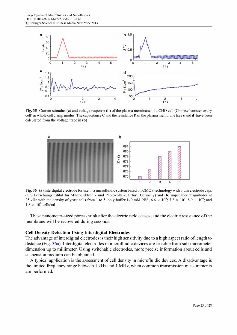
These nanometer-sized pores shrink after the electric field ceases, and the electric resistance of themembrane will be recovered during seconds.
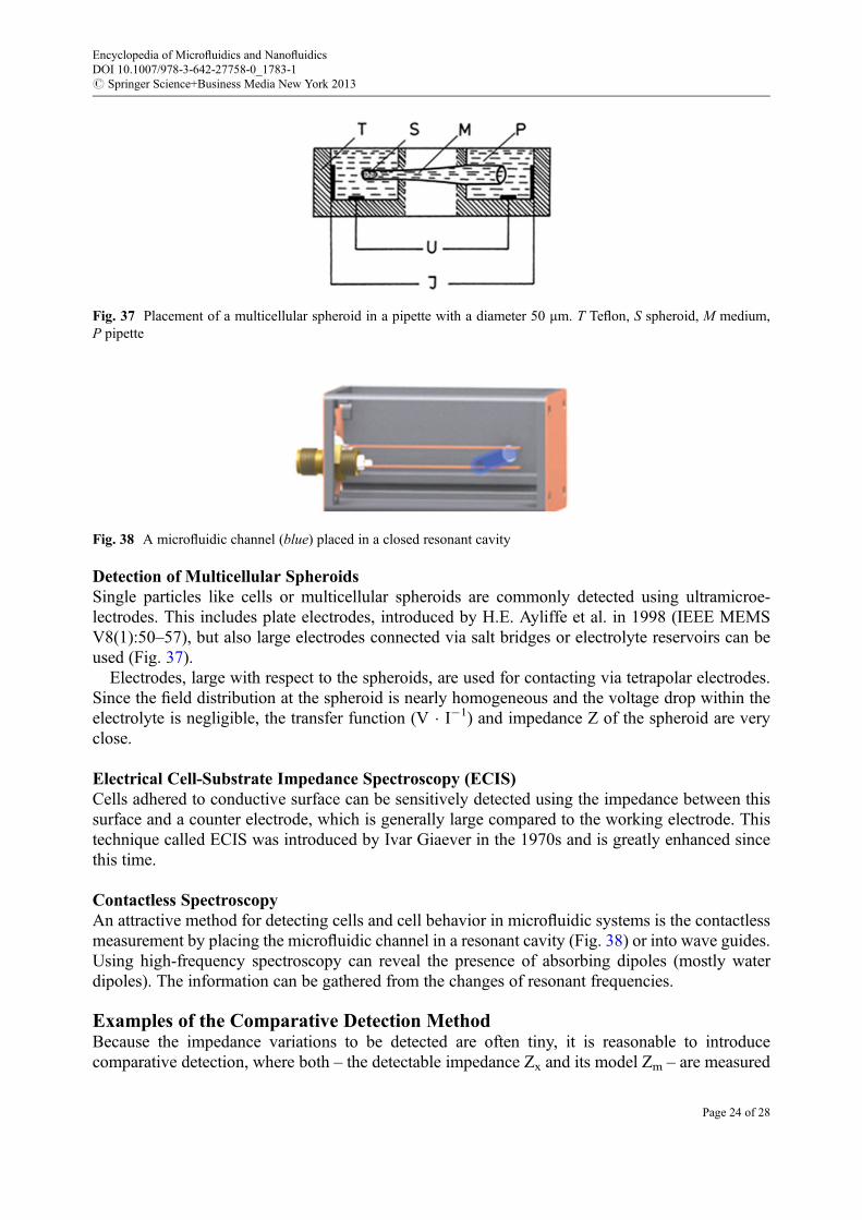
Cell Density Detection Using Interdigital ElectrodesThe advantage of interdigital electrodes is their high sensitivity due to a high aspect ratio of length todistance (Fig. 36a). Interdigital electrodes in microfluidic devices are feasible from sub-micrometerdimension up to millimeter. Using switchable electrodes, more precise information about cells andsuspension medium can be obtained.
A typical application is the assessment of cell density in microfluidic devices. A disadvantage isthe limited frequency range between 1 kHz and 1 MHz, when common transmission measurementsare performed.
801.5
0.5
1
0
200
150
R /
Ωcm
2
50
100
0
0 1 2 3 4
1 2 3 4 5
U /
V
1.4
0.8
C/ μ
F/c
m2
0.410 2 3 4
0.6
1
1.2
a b
c d
40
I / n
A60
20
00 2
t / s t / s
t / st / s
3 4 51
Fig. 35 Current stimulus (a) and voltage response (b) of the plasma membrane of a CHO cell (Chinese hamster ovarycell) in whole cell clampmodus. The capacitance C and the resistance R of the plasma membrane (see c and d) have beencalculated from the voltage trace in (b)
681
680
679
678
677
676
675
1
|Z|/
Ω
2 3 4 5
a b
Fig. 36 (a) Interdigital electrode for use in a microfluidic system based on CMOS technology with 3 mm electrode caps(CiS Forschungsinstitut f€ur Mikroelektronik und Photovoltaik, Erfurt, Germany) and (b) impedance magnitudes at25 kHz with the density of yeast cells from 1 to 5: only buffer 140 mM PBS; 6.6 � 104; 7.2 � 105; 8.9 � 106; and1.8 � 108 cells/ml
Encyclopedia of Microfluidics and NanofluidicsDOI 10.1007/978-3-642-27758-0_1783-1# Springer Science+Business Media New York 2013
Page 23 of 28
Detection of Multicellular SpheroidsSingle particles like cells or multicellular spheroids are commonly detected using ultramicroe-lectrodes. This includes plate electrodes, introduced by H.E. Ayliffe et al. in 1998 (IEEE MEMSV8(1):50–57), but also large electrodes connected via salt bridges or electrolyte reservoirs can beused (Fig. 37).
Electrodes, large with respect to the spheroids, are used for contacting via tetrapolar electrodes.Since the field distribution at the spheroid is nearly homogeneous and the voltage drop within theelectrolyte is negligible, the transfer function (V � I�1) and impedance Z of the spheroid are veryclose.
Electrical Cell-Substrate Impedance Spectroscopy (ECIS)Cells adhered to conductive surface can be sensitively detected using the impedance between thissurface and a counter electrode, which is generally large compared to the working electrode. Thistechnique called ECIS was introduced by Ivar Giaever in the 1970s and is greatly enhanced sincethis time.
Contactless SpectroscopyAn attractive method for detecting cells and cell behavior in microfluidic systems is the contactlessmeasurement by placing the microfluidic channel in a resonant cavity (Fig. 38) or into wave guides.Using high-frequency spectroscopy can reveal the presence of absorbing dipoles (mostly waterdipoles). The information can be gathered from the changes of resonant frequencies.
Examples of the Comparative Detection MethodBecause the impedance variations to be detected are often tiny, it is reasonable to introducecomparative detection, where both – the detectable impedance Zx and its model Zm – are measured
Fig. 37 Placement of a multicellular spheroid in a pipette with a diameter 50 mm. T Teflon, S spheroid, M medium,P pipette
Fig. 38 A microfluidic channel (blue) placed in a closed resonant cavity
Encyclopedia of Microfluidics and NanofluidicsDOI 10.1007/978-3-642-27758-0_1783-1# Springer Science+Business Media New York 2013
Page 24 of 28

and the results are compared (Fig. 39), see also Fig. 33 and Table 1. In this way the deviationsDZx ¼ Zx – Zm can be detected with high sensitivity and resolution [6, 7].
Single-Cell Detection Based on Comparative MethodBioimpedance based on high-throughput single-cell analysis methods is being developed forcounting and characterizing a large number of single cells at high speed (Figs. 40 and 41).Depending on the specific task, conductivity and capacity or dielectric dispersions of permittivityin suspension are measured [7].
Figure 40 gives an electrical solution for the single-cell detection with coplanar electrodes. Suchtechnique is easy to implement but has poor sensitivity due to noneffective using of distorted electricfield between the electrodes.
Figure 41 gives an impedimetric setup for single-cell detection with two pairs of parallelelectrodes [7]. Though the electrode system is more complicated in comparison with coplanarplacement of electrodes in Fig. 40, this solution is much more resultful. The sensitivity is increasedbecause of more targeted and homogeneous electrical field between the upper and lower electrodes,and thanks to effective compensation of electrode polarization.
Fig. 39 A setup for the comparative measurement of the impedance deviation DZx
Fig. 40 Comparative detection of cell impedance via differential measurement with the aid of coplanar electrodes
Encyclopedia of Microfluidics and NanofluidicsDOI 10.1007/978-3-642-27758-0_1783-1# Springer Science+Business Media New York 2013
Page 25 of 28

Such a solution similar to Fig. 33c has been in use in the Southampton University, UK [7]. Exci-tation signal used in [7] is a pseudorandom sequence of binary pulses – the maximum lengthsequence MLS, see Fig. 27, enabling to perform fast and wide band impedance spectroscopy. Theresponse signal is processed using a cross-correlation technique, and the fast Fourier transform(FFT) is applied for getting the impedance spectra in frequency domain; see Fig. 17a.
Fig. 41 Comparative detection of cell impedance via differential measurement by the aid of parallel electrodes
Glass microtube
Electrical Model
IM
If the model is ideal, then ΔV=0 in the beginning of measurement
Vexc
ZM
ZX
2κΔV ~ ΔZX
2κ
20κ
1κ
Fig. 42 Electronic circuit for the detection of difference between the impedance Zx and of its electrical model ZM (seealso Fig. 39)
Encyclopedia of Microfluidics and NanofluidicsDOI 10.1007/978-3-642-27758-0_1783-1# Springer Science+Business Media New York 2013
Page 26 of 28
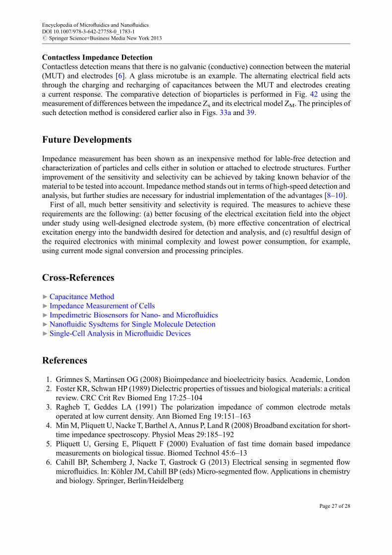
Contactless Impedance DetectionContactless detection means that there is no galvanic (conductive) connection between the material(MUT) and electrodes [6]. A glass microtube is an example. The alternating electrical field actsthrough the charging and recharging of capacitances between the MUT and electrodes creatinga current response. The comparative detection of bioparticles is performed in Fig. 42 using themeasurement of differences between the impedance Zx and its electrical model ZM. The principles ofsuch detection method is considered earlier also in Figs. 33a and 39.
Future Developments
Impedance measurement has been shown as an inexpensive method for lable-free detection andcharacterization of particles and cells either in solution or attached to electrode structures. Furtherimprovement of the sensitivity and selectivity can be achieved by taking known behavior of thematerial to be tested into account. Impedance method stands out in terms of high-speed detection andanalysis, but further studies are necessary for industrial implementation of the advantages [8–10].
First of all, much better sensitivity and selectivity is required. The measures to achieve theserequirements are the following: (a) better focusing of the electrical excitation field into the objectunder study using well-designed electrode system, (b) more effective concentration of electricalexcitation energy into the bandwidth desired for detection and analysis, and (c) resultful design ofthe required electronics with minimal complexity and lowest power consumption, for example,using current mode signal conversion and processing principles.
Cross-References
▶Capacitance Method▶ Impedance Measurement of Cells▶ Impedimetric Biosensors for Nano- and Microfluidics▶Nanofluidic Sysdtems for Single Molecule Detection▶ Single-Cell Analysis in Microfluidic Devices
References
1. Grimnes S, Martinsen OG (2008) Bioimpedance and bioelectricity basics. Academic, London2. Foster KR, Schwan HP (1989) Dielectric properties of tissues and biological materials: a critical
review. CRC Crit Rev Biomed Eng 17:25–1043. Ragheb T, Geddes LA (1991) The polarization impedance of common electrode metals
operated at low current density. Ann Biomed Eng 19:151–1634. MinM, Pliquett U, Nacke T, Barthel A, Annus P, Land R (2008) Broadband excitation for short-
time impedance spectroscopy. Physiol Meas 29:185–1925. Pliquett U, Gersing E, Pliquett F (2000) Evaluation of fast time domain based impedance
measurements on biological tissue. Biomed Technol 45:6–136. Cahill BP, Schemberg J, Nacke T, Gastrock G (2013) Electrical sensing in segmented flow
microfluidics. In: Köhler JM, Cahill BP (eds) Micro-segmented flow. Applications in chemistryand biology. Springer, Berlin/Heidelberg
Encyclopedia of Microfluidics and NanofluidicsDOI 10.1007/978-3-642-27758-0_1783-1# Springer Science+Business Media New York 2013
Page 27 of 28

7. Sun T, Morgan H (2010) Single-cell microfluidic impedance cytometry: a review. MicrofluidNanofluid 8:423–443
8. Yang L, Bashir R (2008) Research review paper: electrical/electrochemical impedance for rapiddetection of foodborne pathogenic bacteria. Biotechnol Adv 26(2):135–150
9. Yang L (2008) Electrical impedance spectroscopy for detection of bacterial cells in suspensionsusing interdigitated microelectrodes. Talanta 74(5):1621–1629
10. Venkatanarayanan A, Keyes TE, Forster RJ (2013) Label-free impedance detection of cancercells. Anal Chem 85:2216–2222
Encyclopedia of Microfluidics and NanofluidicsDOI 10.1007/978-3-642-27758-0_1783-1# Springer Science+Business Media New York 2013
Page 28 of 28